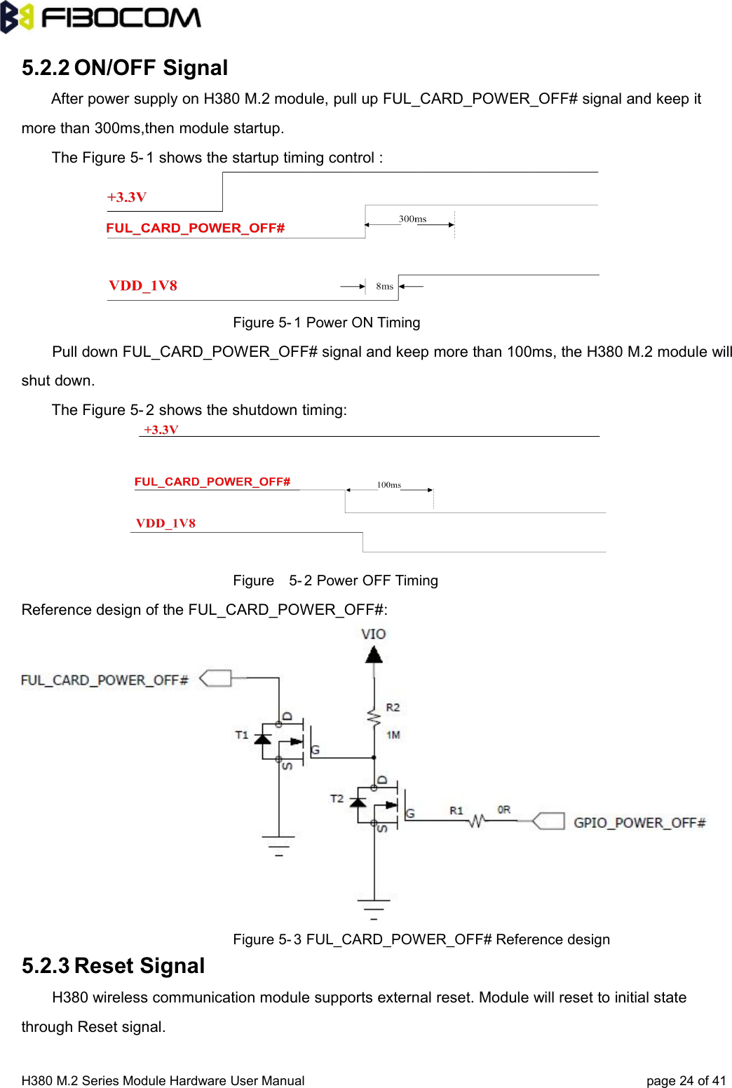
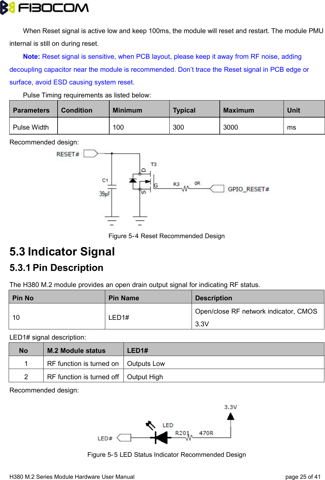
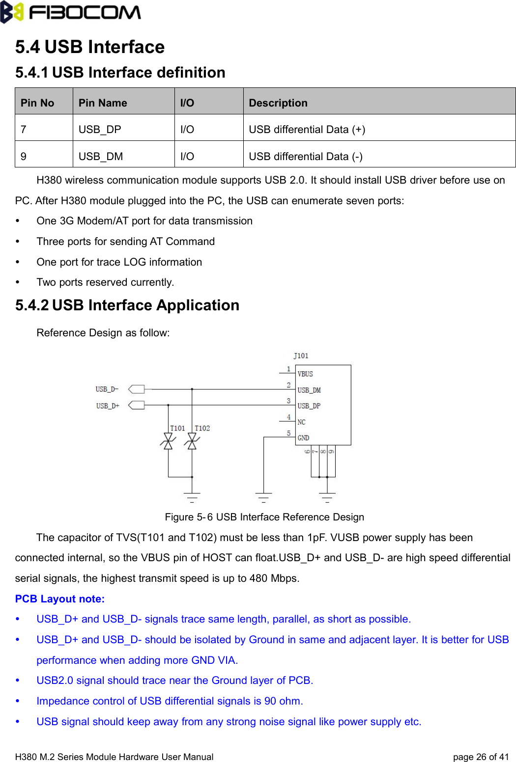
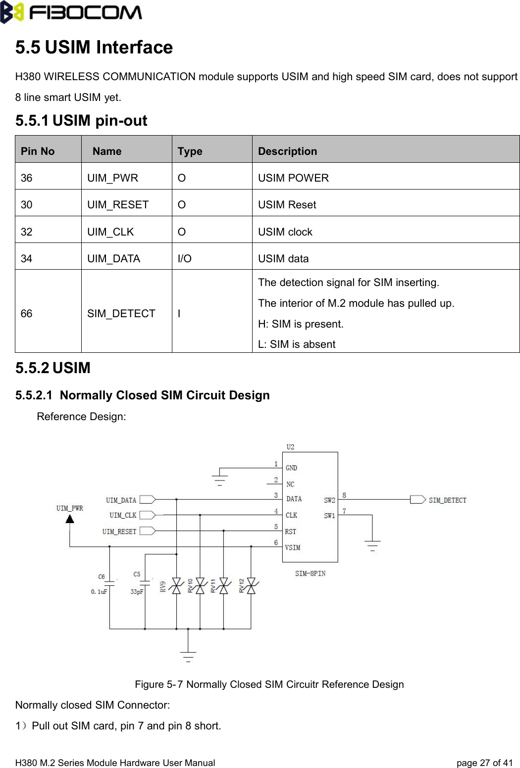
Fibocom Wireless H38F WCDMA Module User Manual
Fibocom Wireless Inc. WCDMA Module
UserManual.wiki
>
Fibocom Wireless
>
H38F User Manual
User Manual
Navigation menu
Upload a User Manual
Namespaces
Wiki Guide
HTML
PDF
Info
Views
User Manual
Discussion / Help
Navigation
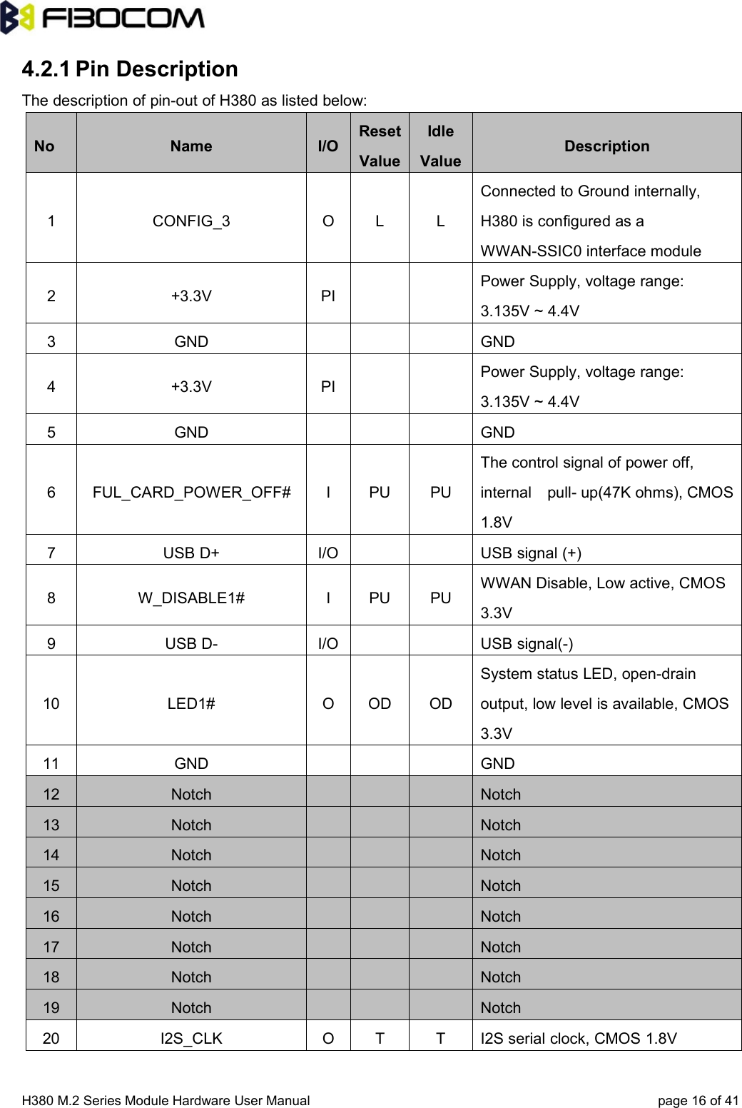
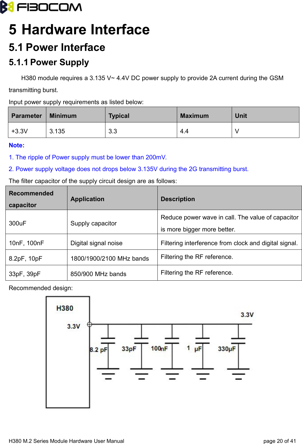
![H380 M.2 Series Module Hardware User Manual page 7of 41PCIe_M.2_Electromechanical_Spec_Rev0.9-3_07312013_RS_Clean[1]](https://usermanual.wiki/Fibocom-Wireless/H38F/User-Guide-2306715-Page-7.png)