Fibocom Wireless H38F WCDMA Module User Manual
Fibocom Wireless Inc. WCDMA Module
User Manual

H380 M.2 Series Module
Hardware User Manual
Version: V1.0.2
Date: 2014-06-04
H380 M.2 Series Module Hardware User Manual page 2of 41
Confidential Material
This document contains information highly confidential to Fibocom Wireless Inc. (Fibocom). Fibocom
offers this information as a service to its customers, to support application and engineering efforts that use
the products designed by Fibocom. The information provided is based upon requirements specifically
provided to Fibocom by the customers. All specifications supplied herein are subject to change.
Disclosure of this information to other parties is prohibited without the written consent of Fibocom.
Copyright
Copy, Reproduce, Distribute and/or Edit of this document or part of it as well as utilization of its contents
and communication thereof to others without express authorization are prohibited. Offenders will be held
liable for payment of damages. All rights created by patent grant or registration of a utility model or design
patent are reserved. Copyright ©2013 Fibocom Wireless Inc. All rights reserved.
Trademarks Notice
The FIBOCOM Logo is registered by Fibocom Wireless Inc. All other product or service names or logos
are the property of their respective owners. Copyright ©2013 Fibocom Wireless Inc. All rights reserved.
Revision History
Version Date Remarks
V1.0.0 2014-03-20 Initial version
V1.0.1 2014-04-18
1.Change current part.
2.Change GPS part.
3.Change temperature .
V1.0.2 2014-06-04 Add support spec of Win 8 / android dual system switch .
H380 M.2 Series Module Hardware User Manual page 3of 41
Applicability Table
No. Type Note
1 H380-Q50-00
The difference M.2 wireless communication module of H380 series as listed below:
Model No.
GSM/GPRS/EDGE
Band(MHz)
WCDMA Band(MHz)
HSDPA
(Mbps)
HSUPA
(Mbps)
H380-Q50-00 850/900/1800/1900 850/900/1900/2100 21 5.76

H380 M.2 Series Module Hardware User Manual page 4of 41
Contents
1 Preface....................................................................................................................................................................... 6
1.1 Outline............................................................................................................................................................. 6
1.2 Standards....................................................................................................................................................... 6
2 Introduction................................................................................................................................................................ 8
2.1 Description......................................................................................................................................................8
2.2 Specifications................................................................................................................................................. 8
2.3 Appearance.................................................................................................................................................. 10
3 Mechanical............................................................................................................................................................... 11
3.1 Size................................................................................................................................................................ 11
3.2 Application Interface Description.............................................................................................................. 12
3.3 M.2 Connector............................................................................................................................................. 13
4 Hardware Overview................................................................................................................................................14
4.1 Block Diagram............................................................................................................................................. 14
4.2 Pin Definition................................................................................................................................................ 15
Pin Map................................................................................................................................................................15
4.2.1 Pin Description................................................................................................................................. 16
5 Hardware Interface.................................................................................................................................................20
5.1 Power Interface........................................................................................................................................... 20
5.1.1 Power Supply................................................................................................................................... 20
5.1.2 Power Consumption........................................................................................................................21
5.2 The signal of on/off and reset................................................................................................................... 23
5.2.1 Pin Definition.................................................................................................................................... 23
5.2.2 ON/OFF Signal.................................................................................................................................24
5.2.3 Reset Signal..................................................................................................................................... 24
5.3 Indicator Signal............................................................................................................................................25
5.3.1 Pin Description................................................................................................................................. 25
5.4 USB Interface...............................................................................................................................................26
5.4.1 USB Interface definition..................................................................................................................26
5.4.2 USB Interface Application.............................................................................................................. 26
5.5 USIM Interface.............................................................................................................................................27
5.5.1 USIM pin-out.....................................................................................................................................27
5.5.2 USIM.................................................................................................................................................. 27
5.5.3 USIM Design Notice........................................................................................................................28
5.5.4 USIM Hot Plug..................................................................................................................................29
5.6 Digital Audio................................................................................................................................................. 29
5.6.1 I2S Interface Description................................................................................................................ 30

H380 M.2 Series Module Hardware User Manual page 5of 41
5.6.2 I2C Interface Description................................................................................................................30
5.6.3 PCM Mode Interface Description.................................................................................................. 30
5.7 Win8/Android Dual System Switch.......................................................................................................... 31
5.8 W_DISABLE# Interface............................................................................................................................. 31
5.8.1 WWAN_DISABLE# Interface Description................................................................................... 31
5.8.2 GPS_DISABLE# Interface Description........................................................................................ 32
5.9 TX_BLANKING............................................................................................................................................ 32
5.10 Wakeup Host Interface............................................................................................................................ 32
5.11 BODY_SAR Interface............................................................................................................................... 33
5.12 Clock Interface.......................................................................................................................................... 33
5.13 Config..........................................................................................................................................................33
5.14 RF Interface............................................................................................................................................... 34
5.14.1 RF Connector Interface Description...........................................................................................34
5.14.2 RF Connector Description............................................................................................................34
5.14.3 RF Connector main performance index.................................................................................... 35
5.15 Others......................................................................................................................................................... 35
6 Electrical and Environmental................................................................................................................................ 36
6.1 Electrical....................................................................................................................................................... 36
6.2 Environmental..............................................................................................................................................36
7 RF Interface............................................................................................................................................................. 37
7.1 Operating Band........................................................................................................................................... 37
7.1.1 Antenna Band................................................................................................................................... 37
7.1.2 Diversity Antenna Band.................................................................................................................. 37
7.2 RF PCB Design........................................................................................................................................... 37
7.2.1 Impedance Design...........................................................................................................................37
7.3 Antenna Design........................................................................................................................................... 37
7.3.1 Main Antenna Design Requirements........................................................................................... 37
7.3.2 Diversity Antenna Design............................................................................................................... 39
IMPORTANT NOTE.................................................................................................................................................. 40
USERS MANUAL OF THE END PRODUCT....................................................................................................... 40

H380 M.2 Series Module Hardware User Manual page 6of 41
1 Preface
1.1 Outline
The document outlines the electrical, RF performance, mechanical size and application environment
of H380 series M.2 wireless communication module. Under the help of the document and others
application notice, the application developer could understand quickly the performance of H380 series
M.2 wireless communication module,and developing the product.
1.2 Standards
The products`reference design standard as listed below:
3GPP TS 27.007 -v6.9.0: AT command set for User Equipment (UE)
3GPP TS 27.005 -v6.0.1: Use of Data Terminal Equipment -Data Circuit terminating Equipment
(DTE-DCE) interface for Short Message Service (SMS) and Cell Broadcast Service (CBS)
3GPP TS 23.040 -v6.9.0: Technical realization of Short Message Service (SMS)
3GPP TS 24.011 -v6.1.0: Point- to - Point (PP) Short Message Service (SMS) support on mobile
radio interface.
3GPP TS 27.010 -v6.0.0: Terminal Equipment to User Equipment (TE-UE) multiplexer protocol
3GPP TS 27.060 -v6.0.0: Packet domain; Mobile Station (MS) supporting Packet Switched services
3GPP TS 25.304-v6.10.0: User Equipment (UE) procedures in idle mode and procedures for cell
reselection in connected mode.
3GPP TS 25.308 -v6.4.0: High Speed Downlink Packet Access (HSDPA); Overall description;Stage
2.
3GPP TS 25.309 -v6.6.0: FDD enhanced uplink; Overall description; Stage 2.
3GPP TS 23.038 -v6.1.0: Alphabets and language - specific information
3GPP TS 21.111 -v6.3.0: USIM and IC card requirements.
3GPP TS 31.111 -v6.11.0 "USIM Application Toolkit (USAT)".
3GPP TS 45.002 -v6.12.0: Multiplexing and multiple access on the radio path.
3GPP TS 51.014 -v4.5.0: Specification of the SIM Application Toolkit for the Subscriber Identity
Module - Mobile Equipment (SIM-ME) interface.
3GPP TS 51.010 -1 -v6.7.0: Mobile Station (MS) conformance specification; Part 1: Conformance
specification.
3GPP TS 22.004 -v6.0.0: General on supplementary services.
3GPP TS 23.090 -v6.1.0: Unstructured Supplementary Service Data (USSD); Stage 2
3GPP TS 24.008 v6.19, Mobile radio interface Layer 3 specification;

H380 M.2 Series Module Hardware User Manual page 7of 41
PCIe_M.2_Electromechanical_Spec_Rev0.9-3_07312013_RS_Clean[1]
H380 M.2 Series Module Hardware User Manual page 8of 41
2 Introduction
2.1 Description
H380 M.2 series modules are highly integrated 3G wireless communication modules, support GSM /
GPRS / EDGE and UMTS / HSDPA / HSUPA / HSPA+ , GPS/GNSS(follow-up support ).
2.2 Specifications
Specifications
Bands UMTS (WCDMA/FDD): 850/900/1900/2100MHz
GSM/GPRS/EDGE: 850/900/1800/1900MHz
Data
UMTS/HSDPA/HSUPA 3GPP release 7
HSUPA 5.76Mbps (Cat 6)
HSDPA 21Mbps (Cat 14) or 7.2Mbps (Cat 8)
GSM 3GPP release 7
EDGE (E-GPRS) multi-slot class 33(296kbps DL, 236.8kbps UL)
GPRS multi-slot class 33(107kbps DL, 85.6kbps UL)
GPS GPS/GNSS(follow-up support)
Physical
Dimension: 22mm x 42mm x 2.35mm
Interface: M.2
Weight: 5.0 grams
Environment
Operating Temperature: -30℃~ +75℃
Storage Temperature: -40℃~ +85℃
Performance
Operating
Voltage
Voltage: 3.135V ~ 4.4V Normal: 3.3V
Operating
Current
(Typical Value)
3mA (Sleep Mode)
3G Talk: 660mA
2G Talk: 270mA (GSM PCL5)
Transmit Power
(Typical Value)
Class 4 (2W): 850/900 MHz, GSM
Class 1 (1W): 1800/1900 MHz, GSM
Class E2 (0.6W): 850/900 MHz, EDGE
Class E2 (0.5W): 1800/1900 MHz, EDGE
H380 M.2 Series Module Hardware User Manual page 9of 41
Class 3 (0.25W): 900/850/1900/2100 MHz, WCDMA
Rx Sensitivity
(Typical Value)
UMTS/HSPA: -109dBm
GSM: -108dBm
Interfaces
RF Interface Main Antenna, Diversity Antenna(RF diversity and GPS Aux)
Connectivity
1 x USB 2.0,Multiple Profiles over USB
I2C Support,I2S/PCM Support
GPIO Connectivity
Data Features
Protocol Stack Embedded TCP/IP and UDP/IP protocol stack
EDGE
Multi-slot class 33(5 Down; 4 Up; 6 Total)
Coding Scheme MCS1~9
GPRS
Multi-slot class 33(5 Down; 4 Up; 6 Total)
Coding Scheme CS1~4
CSD UMTS(14.4kbps), GSM(9.6kbps)
USSD Support
SMS
MO / MT Text and PDU modes
Cell broadcast
Voice Features
Digital Audio
Voice coders: EFR/HR/FR/AMR
Audio Control Gain Control
Character Set
IRA
GSM
UCS2
HEX
AT Commands
FIBOCOM proprietary AT commands
GSM 07.05
GSM 07.07
Accessories
Firmware Loader Tool over USB/UART
User Manual
Developer Kit
H380 M.2 Series Module Hardware User Manual page 10 of 41
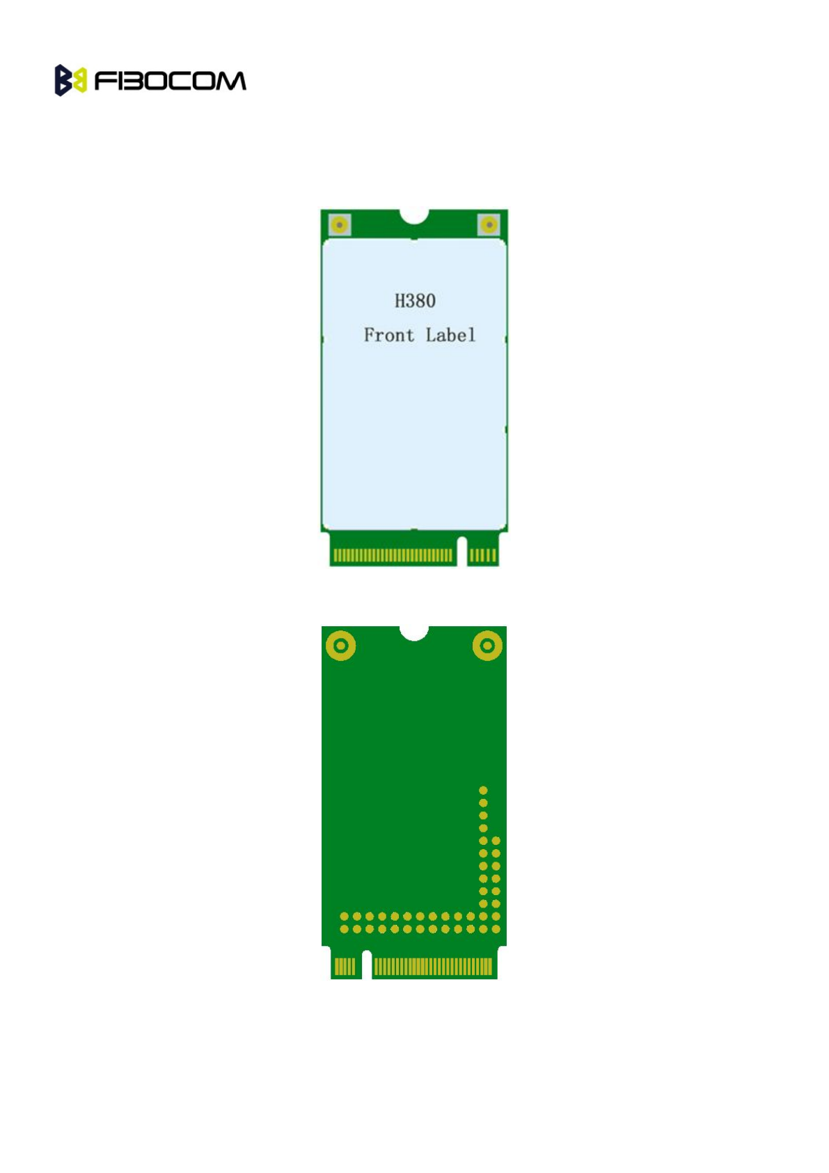
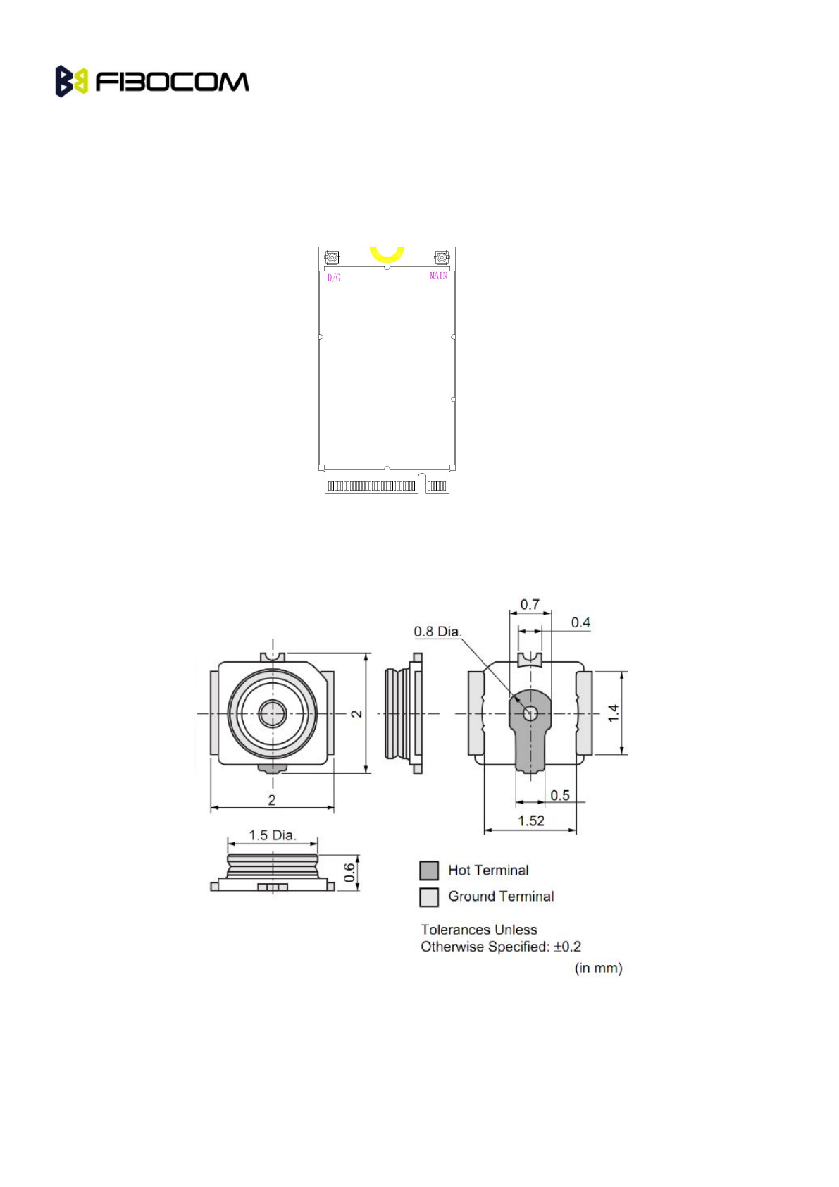
2.3 Appearance
The following picture shows the H380 M.2 WWAN Module.
Top view:
Figure 2- 1 Top View
Bottom view:
Figure 2- 2 Bottom View
H380 M.2 Series Module Hardware User Manual page 11 of 41
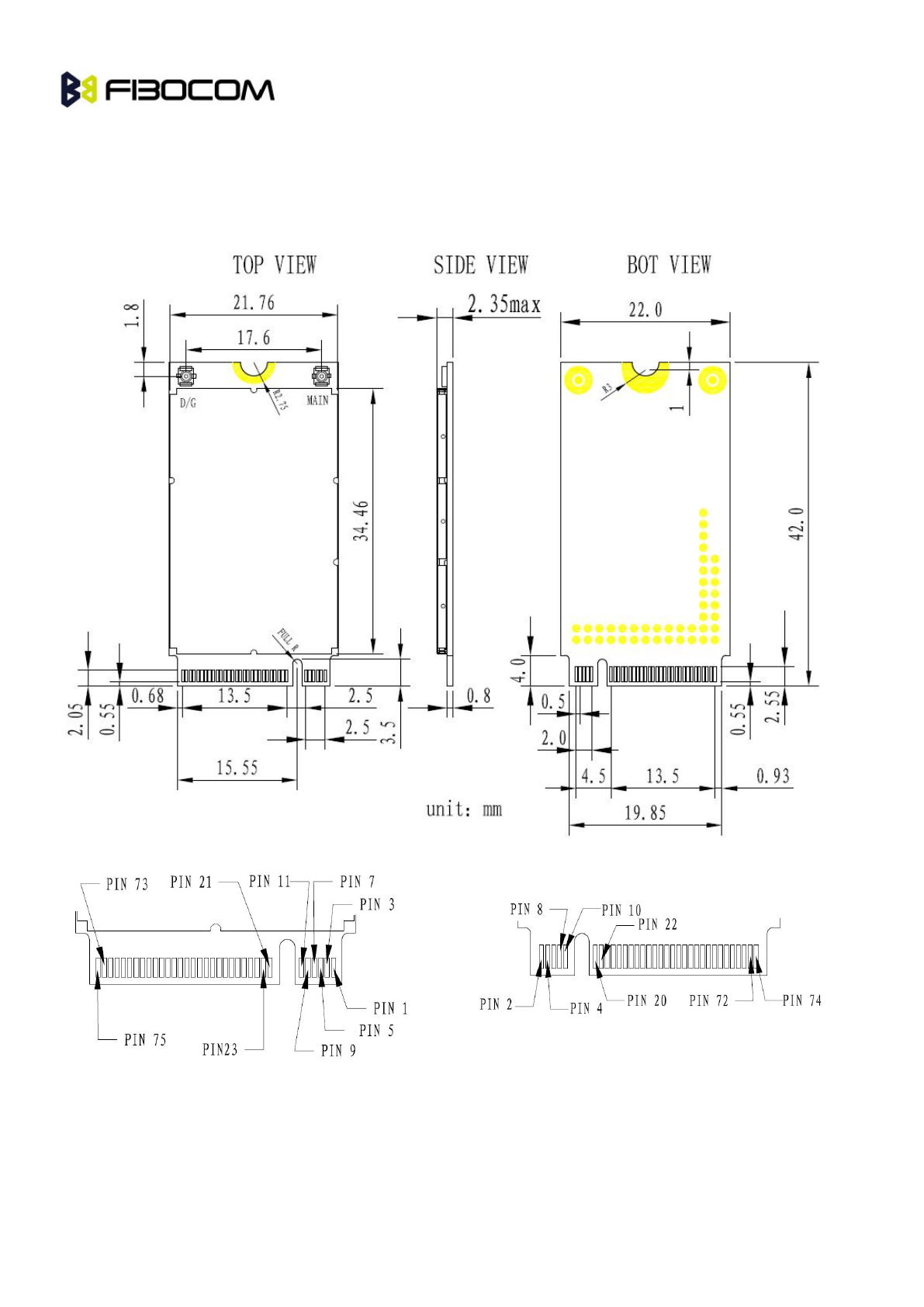
3 Mechanical
3.1 Size
Figure 3- 1 Mechanical size
H380 M.2 Series Module Hardware User Manual page 12 of 41
3.2 Application Interface Description
H380 M.2 module uses 75-pin gold fingers as the external interface,the size of the module please
refer to the Section3.1.
As shown in Figure 4-2, H380 M.2 module uses the 75-pin fingers interface(67 pin is signal interface
and 8 is notch).
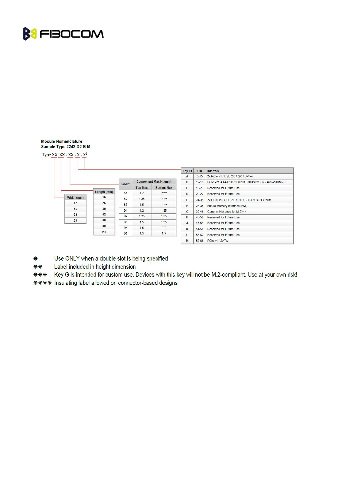
About the naming rules of M.2, H380 uses the Type 2242-S3-B (22mmx42mm,Top surface element
layer maximum thickness is 1.5mm, the thickness of PCB is 0.8mm, Key ID is B)
H380 M.2 Series Module Hardware User Manual page 13 of 41
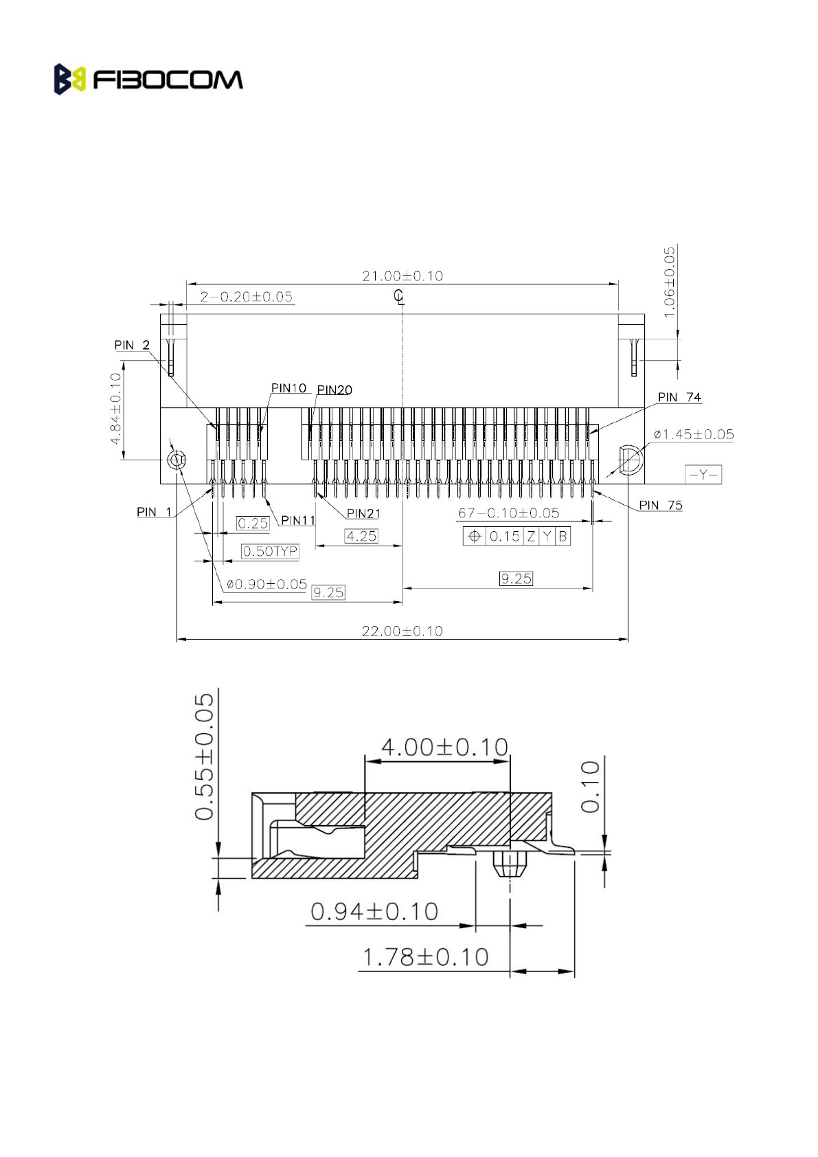
3.3 M.2 Connector
Recommended to use the M.2 connector from LOTES, type is APCI0026-P001A,the Connector
package design please refer to the relevant specifications and design.
As shown in Figure 3-2::
Figure 3- 2 APCI0026-P001A M.2 connector dimension
H380 M.2 Series Module Hardware User Manual page 14 of 41
4 Hardware Overview
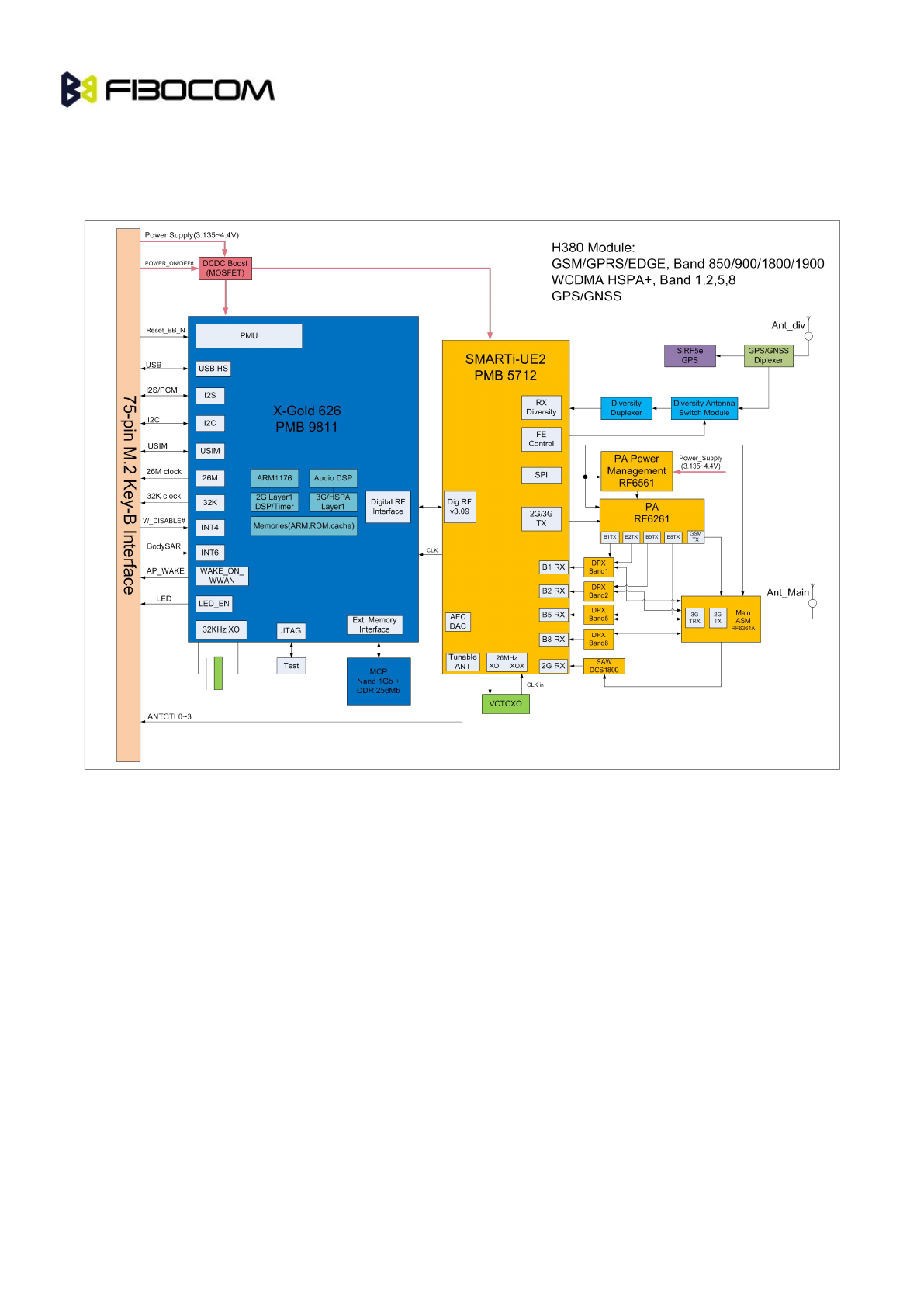
4.1 Block Diagram
Figure 4- 1 Block Diagram
H380 M.2 Series Module Hardware User Manual page 15 of 41
4.2 Pin Definition
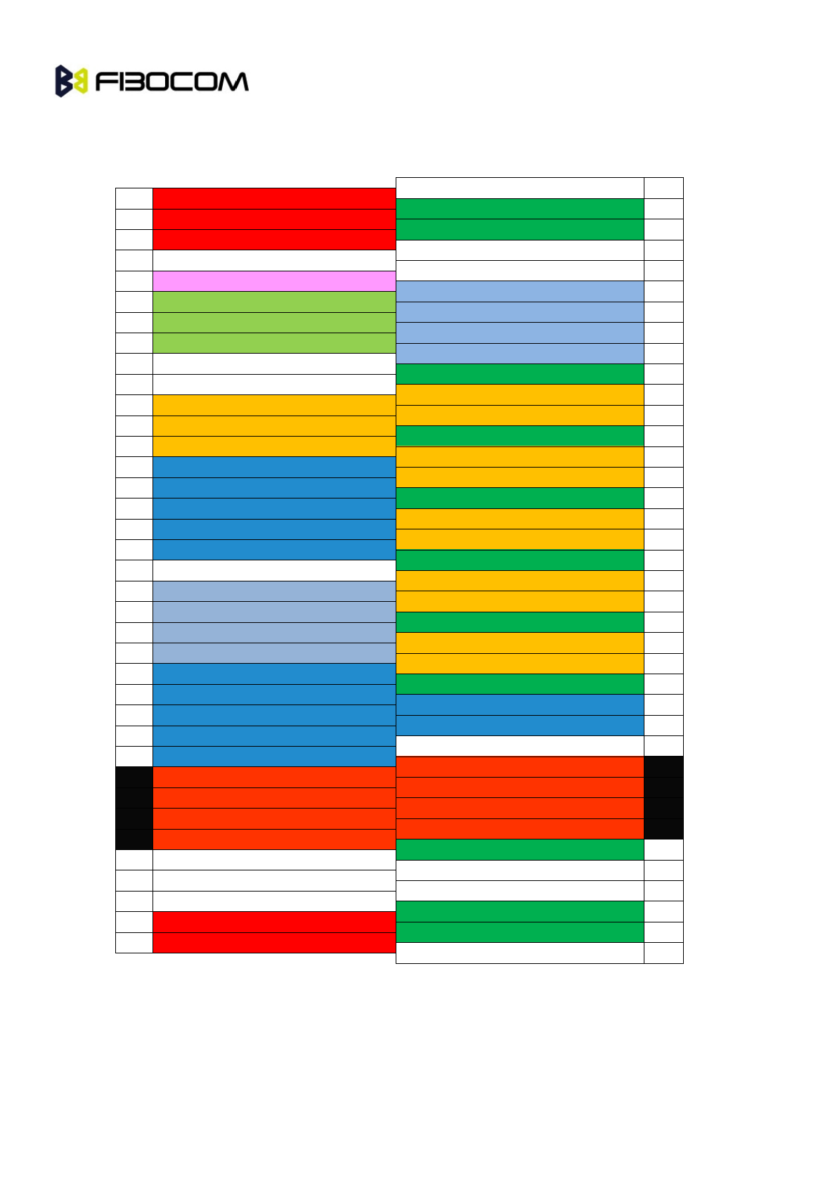
Pin Map
CONFIG_2
75
74
+3.3V
GND
73
72
+3.3V
GND
71
70
+3.3V
CONFIG_1
69
68
CLK32K
RESET#
67
66
SIM_DETECT
ANTCTL3
65
64
NC
ANTCTL2
63
62
NC
ANTCTL1
61
60
NC
ANTCTL0
59
58
NC
GND
57
56
NC
NC
55
54
NC
NC
53
52
NC
GND
51
50
NC
NC
49
48
TX_BLANKING
NC
47
46
SYSCLK
GND
45
44
GNSS_IRQ
NC
43
42
GNSS_SDA
NC
41
40
GNSS_SCL
GND
39
38
NC
NC
37
36
UIM_PWR
NC
35
34
UIM_DATA
GND
33
32
UIM_CLK
NC
31
30
UIM_RESET
NC
29
28
I2S_WA
GND
27
26
W_DISABLE2#
DPR
25
24
I2S_RX
WOWWAN#
23
22
I2S_TX
CONFIG_0
21
20
I2S_CLK
Notch
Notch
Notch
Notch
Notch
Notch
Notch
Notch
GND
11
10
LED1#(3.3V)
USB D-
9
8
W_DISABLE1#(3.3V)
USB D+
7
6
FUL_CARD_POWER_OFF#(1.8V)
GND
5
4
+3.3V
GND
3
2
+3.3V
CONFIG_3
1
Figure 4- 2 Pin Definition
H380 M.2 Series Module Hardware User Manual page 16 of 41
4.2.1 Pin Description
The description of pin-out of H380 as listed below:
No Name I/O
Reset
Value
Idle
Value
Description
1 CONFIG_3 O L L
Connected to Ground internally,
H380 is configured as a
WWAN-SSIC0 interface module
2 +3.3V PI
Power Supply, voltage range:
3.135V ~ 4.4V
3 GND GND
4 +3.3V PI
Power Supply, voltage range:
3.135V ~ 4.4V
5 GND GND
6 FUL_CARD_POWER_OFF# I PU PU
The control signal of power off,
internal pull- up(47K ohms), CMOS
1.8V
7 USB D+ I/O USB signal (+)
8 W_DISABLE1# I PU PU
WWAN Disable, Low active, CMOS
3.3V
9 USB D- I/O USB signal(-)
10 LED1# O OD OD
System status LED, open-drain
output, low level is available, CMOS
3.3V
11 GND GND
12 Notch Notch
13 Notch Notch
14 Notch Notch
15 Notch Notch
16 Notch Notch
17 Notch Notch
18 Notch Notch
19 Notch Notch
20 I2S_CLK O T T I2S serial clock, CMOS 1.8V

H380 M.2 Series Module Hardware User Manual page 17 of 41
No
Name I/O
Reset
Value
Idle
Value
Description
21 CONFIG_0 NC
22 I2S_TX O T T I2S serial data output, CMOS 1.8V
23 WOWWAN# O PU PU
The signal of module wake up the
Host device, low level is available,
CMOS 1.8V
24 I2S_RX I T T I2S serial data input, CMOS 1.8V
25 DPR I Body SAR Detect,CMOS 1.8V
26 W_DISABLE2# I PU PU
GPS Disable,active low,CMOS 1.8V
(not support now)
27 GND GND
28 I2S_WA O T T
I2S Left/Right clock signal,CMOS
1.8V
29 NC NC
30 UIM_RESET O PP PP USIM card reset
31 NC NC
32 UIM_CLK O PP PP USIM card clock
33 GND GND
34 UIM_DATA I/O PU PU
USIM card data,
internal 4.7K resistor pull up
35 NC NC
36 UIM_PWR O SIM Card power output,1.8V/3.0V
37 NC NC
38 NC NC
39 GND GND
40 GNSS_SCL O PD PD
Android/Win8 system can switch
INTIN signal, internal resistance was
pulled-up10K, CMOS 1.8V
41 NC NC
42 GNSS_SDA I/O PU PU
I2C serial data,internal pull-up(4.7K
ohms),CMOS 1.8V
43 NC NC

H380 M.2 Series Module Hardware User Manual page 18 of 41
No
Name I/O
Reset
Value
Idle
Value
Description
44 GNSS_IRQ I PU PU
Android/Win8 I2C interrupt request
(not support now), CMOS 1.8V
45 GND GND
46 SYSCLK O L L 26MHz clock output
47 NC NC
48 TX_BLANKING O L L
GSM TDMA Timer output signal,
external GPS control signal, CMOS
1.8V
49 NC NC
50 NC NC
51 GND GND
52 NC NC
53 NC NC
54 NC NC
55 NC NC
56 NC NC
57 GND GND
58 NC NC
59 ANTCTL0 O L L
Tunable antenna control signal,
bit0,CMOS 1.8V(not support now)
60 NC NC
61 ANTCTL1 O L L
Tunable antenna control signal,
bit1, CMOS 1.8V (not support now)
62 NC NC
63 ANTCTL2 O L L
Tunable antenna control signal,
bit2,CMOS 1.8V(not support now)
64 NC NC
65 ANTCTL3 O L L
Tunable antenna control signal,
bit3,CMOS 1.8V(not support now)
66 SIM_DETECT I SIM Detect ,CMOS 1.8V
67 RESET# I PU PU External reset signal input, CMOS

H380 M.2 Series Module Hardware User Manual page 19 of 41
No
Name I/O
Reset
Value
Idle
Value
Description
1.8V
68 CLK32K O 32KHz Clock output
69 CONFIG_1 O L L
Connected to Ground internally,
H380 is configured as a
WWAN-SSIC0 interface module
70 +3.3V PI
The main power supply, voltage
range: 3.135V ~ 4.4V
71 GND GND
72 +3.3V PI
The main power supply, voltage
range: 3.135V ~ 4.4V
73 GND GND
74 +3.3V PI
The main power supply,voltage
range: 3.135V ~ 4.4V
75 CONFIG_2 O L L
Connected to Ground internally,
H380 is configured as a
WWAN-SSIC0 interface module
PI: Power Input
H: High Voltage Level
L: Low Voltage Level
PD: Pull-Down
PU: Pull-Up
T: Tristate
OD: Open Drain
PP: Push-Pull
H380 M.2 Series Module Hardware User Manual page 20 of 41
5 Hardware Interface
5.1 Power Interface
5.1.1 Power Supply
H380 module requires a 3.135 V~ 4.4V DC power supply to provide 2A current during the GSM
transmitting burst.
Input power supply requirements as listed below:
Parameter Minimum Typical Maximum Unit
+3.3V 3.135 3.3 4.4 V
Note:
1. The ripple of Power supply must be lower than 200mV.
2. Power supply voltage does not drops below 3.135V during the 2G transmitting burst.
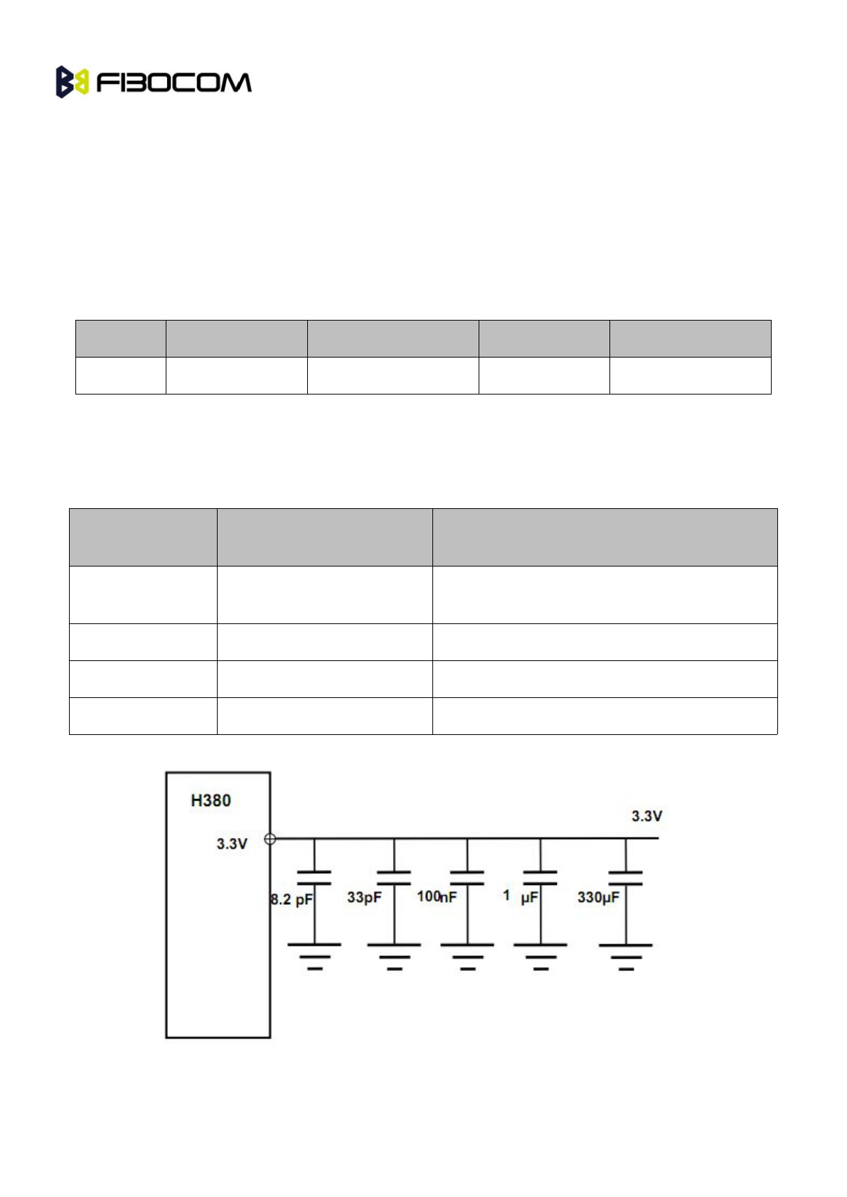
The filter capacitor of the supply circuit design are as follows:
Recommended
capacitor
Application Description
300uF Supply capacitor
Reduce power wave in call. The value of capacitor
is more bigger more better.
10nF, 100nF Digital signal noise Filtering interference from clock and digital signal.
8.2pF, 10pF 1800/1900/2100 MHz bands
Filtering the RF reference.
33pF, 39pF 850/900 MHz bands
Filtering the RF reference.
Recommended design:
H380 M.2 Series Module Hardware User Manual page 21 of 41
5.1.2 Power Consumption
Parameter Description Condition
Typical Value
(3.3V power supply)
Unit
IOFF RTC mode 100 uA
ISLEEP
Low power mode
(GSM)
DRX
22.86
52.56 mA
92.26
Low power mode
(WCDMA)
DRX
63.16
mA8 2.46
92.36
IGSM-RMS
GSM voice -
1 TX slot
1 RX slot Peak
current
During TX slot
GSM850 PCL
5265.4
mA
10 104.2
15 73.6
19 69.2
EGSM900 PCL
5270.2
10 107.0
15 73.9
19 69.2
DCS1800 PCL
0185.8
594.1
10 71.4
15 67.7
PCS1900 PCL
0187.8
597.3
10 72.7
15 69.7
IGSM-MAX
GSM850 PCL
51999.9
mA
10 507.5
15 177.6
19 141.3
EGSM900 PCL
52189.2
10 503.9
15 194.1
H380 M.2 Series Module Hardware User Manual page 22 of 41
Parameter
Description Condition
Typical Value
(3.3V power supply)
Unit
19 157.2
DCS1800 PCL
01335.8
5394.6
10 165.3
15 140.9
PCS1900 PCL
01473.1
5395.7
10 178.9
15 149.7
IGPRS
GSM850 PCL=5
GSM voice -
1RX slot TX
slot
1271.8
mA
4408.3
GSM850 PCL=10
191.8
4232.4
EGSM900 PCL=5
1251.7
4428.1
EGSM900 PCL=10
190.6
4234.3
DCS1800 PCL=0
1175.7
4305.3
DCS1800 PCL=10
178.8
4123.0
PCS1900 PCL=0
1205.2
4326.1
PCS1900 PCL=10
178.8
4124.1
IEGPRS-RMS
GSM850 PCL=8
GSM voice -
1RX slot TX
slot
1216.5
mA
4581.1
GSM850 PCL=15
182.2
4130.6
EGSM900 PCL=8
1213.2
4578.9
H380 M.2 Series Module Hardware User Manual page 23 of 41
Parameter
Description Condition
Typical Value
(3.3V power supply)
Unit
EGSM900 PCL=15
188.7
4156.7
DCS1800 PCL=2
1230.7
4565.6
DCS1800 PCL=10
187.9
4134.0
PCS1900 PCL=2
1234.7
4582.7
PCS1900 PCL=10
187.1
4133.1
IWCDMA-RMS WCDMA
Band1
24dBm 639.4
mA
10dBm 202.3
1dBm 148.0
Band2
24dBm 662.4
10dBm 200.4
1dBm 148.7
Band5
24dBm 442.9
10dBm 180.8
1dBm 142.7
Band8
24dBm 492.0
10dBm 183.0
1dBm 148.4
5.2 The signal of on/off and reset
5.2.1 Pin Definition
H380 wireless communication module has two control signals: power on/off and reset.
Pin Definition as listed below:
Pin No Pin Name Electrical Level Description
6
FUL_CARD_POWER
_OFF#
CMOS 1.8V Power on/off signal
67 RESET# CMOS 1.8V External reset signal input
H380 M.2 Series Module Hardware User Manual page 24 of 41
5.2.2 ON/OFF Signal
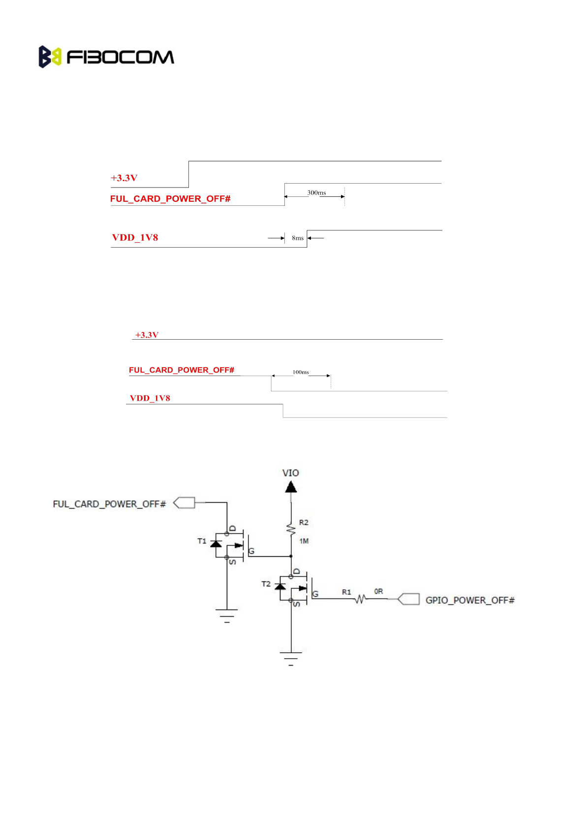
After power supply on H380 M.2 module, pull up FUL_CARD_POWER_OFF# signal and keep it
more than 300ms,then module startup.
The Figure 5- 1 shows the startup timing control :
Figure 5- 1 Power ON Timing
Pull down FUL_CARD_POWER_OFF# signal and keep more than 100ms, the H380 M.2 module will
shut down.
The Figure 5- 2 shows the shutdown timing:
Figure 5- 2 Power OFF Timing
Reference design of the FUL_CARD_POWER_OFF#:
Figure 5- 3 FUL_CARD_POWER_OFF# Reference design
5.2.3 Reset Signal
H380 wireless communication module supports external reset. Module will reset to initial state
through Reset signal.
H380 M.2 Series Module Hardware User Manual page 25 of 41
When Reset signal is active low and keep 100ms, the module will reset and restart. The module PMU
internal is still on during reset.
Note: Reset signal is sensitive, when PCB layout, please keep it away from RF noise, adding
decoupling capacitor near the module is recommended. Don’t trace the Reset signal in PCB edge or
surface, avoid ESD causing system reset.
Pulse Timing requirements as listed below:
Parameters Condition Minimum Typical Maximum Unit
Pulse Width 100 300 3000 ms
Recommended design:
Figure 5- 4 Reset Recommended Design
5.3 Indicator Signal
5.3.1 Pin Description
The H380 M.2 module provides an open drain output signal for indicating RF status.
Pin No Pin Name Description
10 LED1#
Open/close RF network indicator, CMOS
3.3V
LED1# signal description:
No M.2 Module status LED1#
1 RF function is turned on Outputs Low
2 RF function is turned off Output High
Recommended design:
Figure 5- 5 LED Status Indicator Recommended Design
H380 M.2 Series Module Hardware User Manual page 26 of 41
5.4 USB Interface
5.4.1 USB Interface definition
Pin No Pin Name I/O Description
7 USB_DP I/O USB differential Data (+)
9 USB_DM I/O USB differential Data (-)
H380 wireless communication module supports USB 2.0. It should install USB driver before use on
PC. After H380 module plugged into the PC, the USB can enumerate seven ports:
One 3G Modem/AT port for data transmission
Three ports for sending AT Command
One port for trace LOG information
Two ports reserved currently.
5.4.2 USB Interface Application
Reference Design as follow:
Figure 5- 6 USB Interface Reference Design
The capacitor of TVS(T101 and T102) must be less than 1pF. VUSB power supply has been
connected internal, so the VBUS pin of HOST can float.USB_D+ and USB_D- are high speed differential
serial signals, the highest transmit speed is up to 480 Mbps.
PCB Layout note:
USB_D+ and USB_D- signals trace same length, parallel, as short as possible.
USB_D+ and USB_D- should be isolated by Ground in same and adjacent layer. It is better for USB
performance when adding more GND VIA.
USB2.0 signal should trace near the Ground layer of PCB.
Impedance control of USB differential signals is 90 ohm.
USB signal should keep away from any strong noise signal like power supply etc.
H380 M.2 Series Module Hardware User Manual page 27 of 41
5.5 USIM Interface
H380 WIRELESS COMMUNICATION module supports USIM and high speed SIM card, does not support
8 line smart USIM yet.
5.5.1 USIM pin-out
Pin No Name Type Description
36 UIM_PWR O USIM POWER
30 UIM_RESET O USIM Reset
32 UIM_CLK O USIM clock
34 UIM_DATA I/O USIM data
66 SIM_DETECT I
The detection signal for SIM inserting.
The interior of M.2 module has pulled up.
H: SIM is present.
L: SIM is absent
5.5.2 USIM
5.5.2.1 Normally Closed SIM Circuit Design
Reference Design:
Figure 5- 7 Normally Closed SIM Circuitr Reference Design
Normally closed SIM Connector:
1)Pull out SIM card, pin 7 and pin 8 short.
H380 M.2 Series Module Hardware User Manual page 28 of 41
2)Insert SIM card, pin 7 and pin 8 disconnect.
5.5.2.2 Normally Open SIM Circuit Design
Reference Design:
Figure 5- 8 Normally Open SIM Connector Reference Design
Normally Open SIM Connector:
1)Pull out SIM card, pin 7 and pin 8 disconnect.
2)Inset SIM card, pin 7 and pin 8 short.
Note:
For improving EMC performance, SIM card connector should be closed to module
Filtering capacitor should be closed to SIM card pin
The interface need ESD protection, ESD should be closed to SIM card pin
USIM_DATA is already pulled up(4.7K ohms) inside the module
SIM_DETECT support SIM hot plug, high level activated default (detect level can be changed by AT
command). If high level is detected, it means SIM card is inserted.
5.5.3 USIM Design Notice
The SIM interface and signals design is extremely important.
There are several design guidelines that must be followed:
The signals of the SIM card layout should be away from any possible EMI noise, such as RF antenna
and digital switching signals.
To ensure signal integrity, the length between SIM interface signals and module should not exceed
100 mm
To avoid crosstalk between USIM_CLK and USIM_IO, it is recommended to route them separately on
the application board, and preferably isolated by Ground layer.

H380 M.2 Series Module Hardware User Manual page 29 of 41
The SIM card signals should be protected by ESD component(low capacitance capacitor, such as
Zener diode). The recommended part no of ESD component is AVR-M1005C080MTAAB (TDK). ESD
component should layout with SIM connector closely.
5.5.4 USIM Hot Plug
H380 supports the detection function of SIM status,and this function can realize SIM hot plug.
5.5.4.1 Hardware Connection
SIM hot plug function need support of SIM_DETECT signal.
When no SIM card, SIM_DETECT is low level; insert SIM, SIM_DETECT is high level.
Explanation:
1) For normally closed SIM connector circuit, as shown in Figure 5-7.SIM_DETECT connects Pin8 (SW2)
of U2, Pin7 (SW1) short GND. When there is no SIM card, SW2 and SW1 short, SW2 is low level. When
SIM card inserted, SW1 and SW2 disconnect, SIM_DETECT is pulled high.
2) For normally open SIM connector circuit, as shown in Figure 5-8. SIM_DETECT connects Pin8 (SW2)
of U2, and it also be pulled low by 47K ohms resistor. Pin 7 is pulled high by 4.7K ohms resistor. When no
SIM card, SW2 and SW1 disconnect, SW2 is low. After SIM inserted, SW2 and SW1 short, SIM_DETECT
is pulled high.
5.5.4.2 Software Configuration
“+MSMPD” AT command control SIM card hot plug function on/off.
AT+MSMPD=0, SIM card hot plug deactivated. Module does not detect SIM_DETECT signal.
AT+MSMPD=1, SIM card hot plug activated. Module support SIM hot plug by SIM_DETECT pin
signal status.
SIM_DETECT High level, SIM card is present, module registers the network automatically.
SIM_DETECT Low level, SIM card is absent, module drops out the network.
Note: The “+MSMPD” default value is “1”. SIM_DETECT is only used for SIM card hot plug detection,
Module don’t detect SIM_DETECT signal at the first startup(it means the module will read SIM card data
and register network at the first startup, no matter pin SIM_DETECT is high or low).
5.6 Digital Audio
H380 M.2 supports digital audio I2S interface. It can support normal I2S mode or PCM mode. The
voltage level of I2S interface is 1.8V.
I2S signal description as listed below:
Pin # Name Type Description
20 I2S_CLK O Clocked
H380 M.2 Series Module Hardware User Manual page 30 of 41
28
I2S_WA O Left/Right clock
22 I2S_TX O data output
24 I2S_RX I data input
42 GNSS_SDA I/O I2C control signal input/output
40 GNSS_SCL O I2C control clock
5.6.1 I2S Interface Description
H380 Signal Direction Audio CODEC I2S Port
I2S2_CLK I2S_CLK
I2S2_WA I2S_LRCK
I2S2_RX I2S_SDIN
I2S2_TX I2S_SDOUT
SYSCLK I2S_MCLK
5.6.2 I2C Interface Description
H380 Signal Direction Audio CODEC I2C Port
GNSS_SDA I2C_SDA
GNSS_SCL I2C_SCL
Note:
I2S support master or slave mode
It supports various audio sample rates (48 KHz, 44.1 KHz, 32 KHz, 24 KHz, 22.5 KHz, 16 KHz, 12
KHz, 11.025 KHz and 8 KHz).
5.6.3 PCM Mode Interface Description
H380 Signal Direction Audio CODEC PCM Port
I2S_CLK (PCM_CLK, PCM clock signal ) PCM_CLK (PCM clock signal)
I2S_WA (PCM_SYNC, PCM frame
synchronization signal )
PCM_SYNC (PCM frame
synchronization signal )
I2S_RX (PCM_DIN, PCM data input) PCM_DOUT (PCM data output)
I2S_TX (PCM_DOUT, PCM data output) PCM_DIN (PCM data input)
H380 M.2 Series Module Hardware User Manual page 31 of 41
Note:
PCM support master or slave mode
PCM support master or slave mode
It supports short frame synchronization of 16 bit, 32bit, 48bit and 64bit.
Supports sending data in burst mode and continuous mode
It supports various audio sample rates (48 KHz, 44.1 KHz, 32 KHz, 24 KHz, 22.5 KHz, 16 KHz, 12
KHz, 11.025 KHz and 8 KHz).
* * The software not support PCM function now!
5.7 Win8/Android Dual System Switch
H380 module supports Win8/Android dual system switch, check and achieve the system switch
through interrupt signal ”GNSS_IRQ”.
NO. Name Type Description
29 GNSS_IRQ I
Win8/Android dual system switch detection signal ,
CMOS 1.8V
Definition of GNSS_IRQ signal function as listed below :
No. GNSS_IRQ Functions
1Low/Floating
Support Win8 system, the module`s USB ports shall set as MBIM
modes.
2High
Support Android system, the module`s `USB ports shall set as 7ACM
modes.
Description:
1. Check and achieve the Win8/Android system switch through GNSS_IRQ level when module boot.
Keep the GNSS_IRQ level stability during booting.
2. Check and achieve the Win8/Android system switch through GNSS_IRQ rising edge/ falling edge, set
ting the de-bouncing time as 100ms. the module will reboot after meeting the requirements and can
switch different system supports.
3. Note:Need high level when switching GNSS_IRQ to android system. Due to internal resistance of
GNSS_IPQ was pulled-up 10K, for achieving high level ,external resistance can not be pulled-up over
20Kohm while circuit design.
5.8 W_DISABLE# Interface
5.8.1 WWAN_DISABLE# Interface Description
H380 module uses the hardware to open / close WWAN RF function signal , the function is also could
H380 M.2 Series Module Hardware User Manual page 32 of 41
controlled by AT command.(please refer to AT manual)
Pin No Name Type Description
8 W_DISABLE1# I WWAN open/close signal, CMOS 3.3V
W_DISABLE# signal function as defined below:
No W_DISABLE# Function
1 Low WWAN function close
2 High WWAN function open
3 Floating WWAN function is defined by AT command , turned on by default
5.8.2 GPS_DISABLE# Interface Description
H380 module uses the hardware to open / close GPS function, the function is also controlled by AT
command.
No Name Type Description
26 W_DISABLE2# I GPS open/close signal, CMOS 1.8V
GPS_DISABLE# function definitions as follow:
No GPS_DISABLE# Function
1 Low GPS function close
2 High GPS function open
3 Floating GPS function is defined by AT command , turned on default
Note: Not support this function now.
5.9 TX_BLANKING
The default value(output) is low. When module works with GSM network, TX Blanking outputs as same
pulse as GSM transmitting burst. To avoid interference with GPS, AP will close GPS or stop GPS
reception when AP detected TX_BLANKING signal.
No Name Type Description
48 TX_BLANKING O External GPS device control signal
5.10 Wakeup Host Interface
H380 M.2 module support wake up the host. Module output low(high default) when need to wake up
the host.
No Name Type Description
H380 M.2 Series Module Hardware User Manual page 33 of 41
23
WOWWAN# O
Module wake up the Host signal ,1.8V signal,
Input low level when wake up Host signal.
5.11 BODY_SAR Interface
H380 M.2 support BODY_SAR function.
BODY_SAR is an input signal (comes from AP output), high default, low active. AP can detect the
closing human body and output BODY_SAR low through proximity sensor. Module will reduce RF
transmitting power by BODY_SAR interrupt.
The threshold transmitting power can be configured by AT command.
No Name Type Description
25 DPR I BODY_SAR detection
5.12 Clock Interface
H380 M.2 support a 26MHz clock output, a 32KHz clock output.
No Name Type Description
46 SYSCLK O
26MHz clock output(for GPS device, as audio codec
MCLK)
68 CLK32K O 32KHz clock output
5.13 Config
H380 M.2 provides 4 configuration pins, the module is configured as WWAN-SSIC 0.
No Name Type Description Value
1 CONFIG_3 O Connected to Ground internally 0
21 CONFIG_0 O NC -
69 CONFIG_1 O Connected to Ground internally 0
75 CONFIG_2 O Connected to Ground internally 0
H380 M.2 Socket 2 Module type configuration as follows:
Config_0
(pin21)
Config_1
(pin69)
Config_2
(pin75)
Config_3
(pin1)
Module Type and Main
Host Interface
Port
Configuration
GND GND GND GND SSD-SATA N/A
GND GND N/C GND WWAN-PCIe N/A
N/C GND GND GND WWAN-SSIC 0
H380 M.2 Series Module Hardware User Manual page 34 of 41
5.14 RF Interface
5.14.1 RF Connector Interface Description
H380 provides two RF interfaces for connecting to the external antenna. D/G is Diversity/GPS Aux
RF antenna, MAIN is RF main antenna.
Figure 5- 9 RF connector diagram
5.14.2 RF Connector Description
H380 M.2 use Murata MM4829-2702 RF connector, 2*2*0.6mm dimension. The connector’s
dimension is as
follow:
Figure 5- 10 RF connector dimension
H380 M.2 Series Module Hardware User Manual page 35 of 41
Figure 5-11 0.81mm coaxial cable matching RF connector
Figure 5-12 the connection between the RF connector and the 0.81 mm cable
5.14.3 RF Connector main performance index
Rated condition Environmental condition
Frequency range DC to 6GHz
Temperature range:
–40°C to +85°C
Characteristic impedance 50Ω
5.15 Others
The interface of GPIO and Tunable ANT of the M.2 module does not support yet..
H380 M.2 Series Module Hardware User Manual page 36 of 41
6 Electrical and Environmental
6.1 Electrical
This table shows the electrical features range of H380 M.2.
Parameter Minimum Value Maximum Value Unit
Power supply 0 4.4 V
Digital Signal 0 1.9 V
6.2 Environmental
This table shows the environmental features of H380 M.2.
Parameter Minimum Value Maximum Value Unit
Operational Temperature -30 +75 °C
Storage Temperature -40 +85 °C
H380 M.2 Series Module Hardware User Manual page 37 of 41
7 RF Interface
7.1 Operating Band
7.1.1 Antenna Band
Operating Band Tx Rx
UMTS 2100 (Band I IMT) 1920–1980 MHz 2110–2170 MHz
UMTS 1900 (Band II IMT) 1850–1910 MHz 1930–1990 MHz
UMTS 850 (Band V IMT) 824–849 MHz 869–894 MHz
UMTS 900 (Band VIII IMT) 880–915 MHz 925–960 MHz
GSM 850 824–849 MHz 869–894 MHz
GSM 900 880–915 MHz 925–960 MHz
DCS 1800 1710–1785 MHz 1805–1880 MHz
PCS 1900 1850–1910 MHz 1930–1990 MHz
7.1.2 Diversity Antenna Band
Operating Band Rx
UMTS 2100 (Band I IMT) 2110–2170 MHz
UMTS 1900 (Band II PCS) 1930–1990 MHz
UMTS 850 (Band V CLR) 869–894 MHz
UMTS 900 (Band VIII GSM) 925–960 MHz
7.2 RF PCB Design
7.2.1 Impedance Design
The impedance of RF should be matched 50 ohm.
7.3 Antenna Design
7.3.1 Main Antenna Design Requirements
(1) Antenna Efficiency
Antenna efficiency is the ratio between antenna input power and radiation power. The radiation power of
an antenna is always lower than the input power due to the following factors: return loss, material loss,

H380 M.2 Series Module Hardware User Manual page 38 of 41
and coupling loss.
Efficiency of the master antenna > 40% (–4dB)
(2) S11 or VSWR
S11 (return loss) indicates the degree to which the input impedance of an antenna matches the reference
impedance (50 ohm). S11 shows the resonance feature and impedance bandwidth of an antenna. Voltage
standing wave ratio (VSWR) is another expression of S11. S11 relates to the antenna efficiency. S11 can
be measured by vector analyzer.
S11 of the master antenna < –10 dB
(3) Polarization
The polarization of an antenna is the orientation of the electric field vector that rotates with time in the
direction of maximum radiation.
Linear polarization is recommended: it would be better if the polarization direction of diversity antenna is
different from main antenna.
(4) Radiation Pattern
Radiation pattern refers to the directional dependence of the strength of radio waves from the antenna or
other source.
The radiation pattern of half wave dipole antennas is the best for wireless terminals. If it is built-in antenna,
PIFA antenna is recommended:
Antenna area (H x W x L): 6mm x 10mm x 100mm. PIFA or IFA antenna is recommended.
Radiation Pattern: Omni-directional
(5) Gain and Directivity
The directivity of the antenna is the electromagnetic field strength of the electromagnetic wave in each
direction. An antenna's power gain is a key performance Figure which combines the antenna’s directivity
and electrical efficiency.
Recommended antenna gain ≤ 2.5dBi
(6) Interference
Besides the antenna performance, the interference on the PCB board also affects the radio performance
(especially the TIS) of the module. To guarantee high performance of the module, the interference
sources on the user board must be properly controlled. On the PCB board, there are various interference
sources that can affect the module, such as the speaker, LCD, CPU, FPC trace and audio circuits, the
power supply should be far away from antenna, notice isolation, shield and filtering processing issues.
(7) TRP/TIS
TRP (Total Radiated Power):

H380 M.2 Series Module Hardware User Manual page 39 of 41
W900/W850/W1900/W2100>19dBm
GSM850/GSM900>28dBm
DCS1800/PCS1900>25dBm
TIS (Total Isotropic Sensitivity) :
W900/W850<-102dBm
W1900/W2100<-103dBm
GSM850/GSM900<-102dBm
DCS1800/PCS1900<-102dBm
7.3.2 Diversity Antenna Design
Diversity reception function of H380 M.2 is optional, Please add a diversity antenna if necessary.
The design methods of diversity antenna and main antenna are the same, its efficiency indicators allows
to reduce 3dB.
The isolation between main antenna and diversity antenna should be higher than 12dB.

H380 M.2 Series Module Hardware User Manual page 40 of 41
IMPORTANT NOTE:
This module is intended for OEM integrator. The OEM integrator is still responsible for the FCC
compliance requirement of the end product, which integrates this module.20cm minimum distance has to
be able to be maintained between the antenna and the users for the host this module is integrated into.
Under such configuration, the FCC radiation exposure limits set forth for an population/uncontrolled
environment can be satisfied.
Any changes or modifications not expressly approved by the manufacturer could void the user's
authority to operate this equipment.
USERS MANUAL OF THE END PRODUCT:
In the users manual of the end product, the end user has to be informed to keep at least 20cm
separation with the antenna while this end product is installed and operated. The end user has to be
informed that the FCC radio-frequency exposure guidelines for an uncontrolled environment can be
satisfied.
The end user has to also be informed that any changes or modifications not expressly approved by
the manufacturer could void the user's authority to operate this equipment. If the size of the end product
is smaller than 8x10cm, then additional FCC part 15.19 statement is required to be available in the users
manual:
This device complies with Part 15 of FCC rules. Operation is subject to the following two conditions:
(1) this device may not cause harmful interference.
(2) this device must accept any interference received, including interference that may cause
undesired operation.
To comply with FCC regulations limiting both maximum RF output power and human exposure to RF
radiation, the maximum antenna gain including cable loss in a mobile-only exposure condition must not
exceed 2.5dBi in the cellular band and 2.5dBi in the PCS band.
A user manual with the end product must clearly indicate the operating requirements and conditions
that must be observed to ensure compliance with current FCC RF exposure guidelines. The end product
with an embedded H380.
Module may also need to pass the FCC Part 15 unintentional emission testing requirements and be
properly authorized per FCC Part 15.
Note: If this module is intended for use in a portable device, you are responsible for separate
approval to satisfy the SAR requirements of FCC Part 2.1093.

H380 M.2 Series Module Hardware User Manual page 41 of 41
LABEL OF THE END PRODUCT:
The final end product must be labeled in a visible area with the following " Contains TX FCC ID:
ZMOH38F ". If the size of the end product is larger than 8x10cm, then the following FCC part 15.19
statement has to also be available on the label: This device complies with Part 15 of FCC rules.
Operation is subject to the following two conditions: (1) this device may not cause harmful
interference and (2) this device must accept any interference received, including interference that may
cause undesired operation.