Fibocom Wireless L811 LTE Module User Manual ng
Fibocom Wireless Inc. LTE Module ng
User Manual

L811-EA Series Module
Hardware User Manual
Version:V1.0.2
Date:2015.09.08
L811-EA Module Hardware User Manual Page
2
of
43
Copyright
Copyright ©2015 Fibocom Wireless Inc . All rights reserved.
Without the prior written permission of the copyright holder, any company or individual is prohibited to
excerpt, copy any part of or the entire document, or transmit the document in any form.
Attention
The document is subject to update from time to time owing to the product version upgrade or other
reasons. Unless otherwise specified, the document only serves as the user guide. All the statements,
information and suggestions contained in the document do not constitute any explicit or implicit
guarantee.
Trademark
The trademark is registered and owned by Fibocom Wireless Inc.
Versions
Version
Date
Remarks
V1.0.0
2014-10-17
Initial Version.
V1.0.1
2015-08-25
Update the logo.
V1.0.2
2015-09-08
Modify descriptions for power on and RTC timing.
L811-EA Module Hardware User Manual Page
3
of
43
Applicable Model List
No.
Type
Note
1
L811-EA
The supported frequency bands of L811-EA wireless modules as shown in the following tables:
Model No.
LTE FDD
WCDMA
GSM/GPRS/EDGE
L811-EA
Band
1,2,3,4,5,7,8,13,17,
18,19,20
Band 1,2,4,5,8
850/900/1800/1900 MHz

L811-EA Module Hardware User Manual Page
4
of
43
Content
1 Foreword.................................................................................................................................................................... 6
1.1 Introduction.....................................................................................................................................................6
1.2 Reference Standard......................................................................................................................................6
2 Product Overview..................................................................................................................................................... 8
2.1 Description......................................................................................................................................................8
2.2 Specifications................................................................................................................................................. 8
2.3 Appearance.................................................................................................................................................. 13
3 Structure...................................................................................................................................................................14
3.1 Dimension Diagram of Structure.............................................................................................................. 14
3.2 Recommended PCB Layout Design........................................................................................................ 15
4 Hardware Introduction........................................................................................................................................... 17
4.1 Pin Definition................................................................................................................................................ 17
4.1.1 Pin Map............................................................................................................................................. 17
4.1.2 Description of Pins...........................................................................................................................18
5 Hardware Interface.................................................................................................................................................24
5.1 Power Interface........................................................................................................................................... 24
5.1.1 Power Supply................................................................................................................................... 24
5.1.2 VSD2_1V8........................................................................................................................................ 24
5.1.3 VRTC................................................................................................................................................. 25
5.2 Power on/off and Reset Signal................................................................................................................. 26
5.2.1 Power on /off Signal........................................................................................................................ 26
5.2.1.1 Power on................................................................................................................................26
5.2.1.2 Power off................................................................................................................................27
5.2.1.3 The Recommended Design of Power on/off................................................................... 28
5.2.2 RESET Signal.................................................................................................................................. 28
5.3 Status Indicating Signals........................................................................................................................... 29
5.3.1 CORE DUMP Indicating................................................................................................................. 29
5.3.2 LPG Signal........................................................................................................................................29
5.3.3 WAKEUP_HOST Signal................................................................................................................. 30
5.3.4 PA_BLANKING Signal....................................................................................................................30
5.4 Interrupt Control Signal.............................................................................................................................. 31
5.4.1 WAKE_UP Signal............................................................................................................................ 31

L811-EA Module Hardware User Manual Page
5
of
43
5.4.2 W_DISABLE# Signal.......................................................................................................................31
5.4.3 Android & Linux / Win8 & Win10 Dual Systems Switch Control Signal................................. 31
5.5 USB Interface...............................................................................................................................................32
5.5.1 USB Interface Definition................................................................................................................. 32
5.5.2 USB Interface Application.............................................................................................................. 33
5.6 UART Interface............................................................................................................................................33
5.6.1 UART Interface Description........................................................................................................... 33
5.6.2 UART Interface Application............................................................................................................34
5.7 USIM Interface.............................................................................................................................................34
5.7.1 USIM Pins......................................................................................................................................... 34
5.7.2 USIM Interface Design....................................................................................................................35
5.7.2.1 “Normally Closed” SIM Card Circuit Design.................................................................... 35
5.7.2.2 “Normally Open” SIM Circuit Design.................................................................................35
5.7.3 Highlights for USIM Design............................................................................................................36
5.7.4 USIM Hot-Plugging..........................................................................................................................36
5.7.4.1 Hardware Connection..........................................................................................................36
5.7.4.2 Software Setup..................................................................................................................... 37
5.8 Digital Audio................................................................................................................................................. 37
5.8.1 I2S Interface..................................................................................................................................... 37
5.8.2 PCM Mode Description...................................................................................................................38
5.9 I2C Interface.................................................................................................................................................38
5.10 Clock Interface.......................................................................................................................................... 39
5.11 Other Interfaces.........................................................................................................................................39
6 Electrical and Environmental Characteristic...................................................................................................... 40
6.1 Electrical Characteristic............................................................................................................................. 40
6.2 Environmental Characteristic.................................................................................................................... 40
7 RF Interface............................................................................................................................................................. 41
7.1 RF PCB Design........................................................................................................................................... 41
7.1.1 Wire Routing Principle.................................................................................................................... 41
7.1.2 Impedance........................................................................................................................................ 42
7.2 Antenna Design........................................................................................................................................... 42
7.2.1 Main Antenna Design Requirements........................................................................................... 42

L811-EA Module Hardware User Manual Page
6
of
43
1 Foreword
1.1 Introduction
The document describes the electrical characteristics, RF performance, dimensions and application
environment, etc. of L811-EA wireless modules. With the assistance of the document and other
instructions, developers can quickly understand the performance of L811-EA wireless modules and
develop products.
1.2 Reference Standard
The design of the product complies with the following standards :
3GPP TS 27.007 -v6.9.0: AT command set for User Equipment (UE)
3GPP TS 27.005 -v6.0.1: Use of Data Terminal Equipment -Data Circuit terminating Equipment
(DTE-DCE) interface for Short Message Service (SMS) and Cell Broadcast Service (CBS)
3GPP TS 23.040 -v6.9.0: Technical realization of Short Message Service (SMS)
3GPP TS 24.011 -v6.1.0: Point- to - Point (PP) Short Message Service (SMS) support on mobile
radio interface
3GPP TS 27.010 -v6.0.0: Terminal Equipment to User Equipment (TE-UE) multiplexer protocol
3GPP TS 27.060 -v6.0.0: Packet domain; Mobile Station (MS) supporting Packet Switched services
3GPP TS 25.304-v6.10.0: User Equipment (UE) procedures in idle mode and procedures for cell
reselection in connected mode
3GPP TS 25.308 -v6.4.0: High Speed Downlink Packet Access (HSDPA); Overall description;
Stage 2
3GPP TS 25.309 -v6.6.0: FDD enhanced uplink; Overall description; Stage 2
3GPP TS 23.038 -v6.1.0: Alphabets and language - specific information
3GPP TS 21.111 -v6.3.0: USIM and IC card requirements
3GPP TS 31.111 -v6.11.0 "USIM Application Toolkit (USAT)"
3GPP TS 45.002 -v6.12.0: Multiplexing and multiple access on the radio path
3GPP TS 51.014 -v4.5.0: Specification of the SIM Application Toolkit for the Subscriber Identity
Module - Mobile Equipment (SIM-ME) interface
3GPP TS 51.010 -1 -v6.7.0: Mobile Station (MS) conformance specification; Part 1: Conformance
specification
3GPP TS 22.004 -v6.0.0: General on supplementary services

L811-EA Module Hardware User Manual Page
7
of
43
3GPP TS 23.090 -v6.1.0: Unstructured Supplementary Service Data (USSD); Stage 2
3GPP TS 24.008 v6.19, Mobile radio interface Layer 3 specification;
3GPP TS 25.101 V7.18.0: User Equipment (UE) radio transmission and reception (FDD)
3GPP TS 36.101V9.18.0: User Equipment (UE) radio transmission and reception
3GPP TS 36.104V9.13.0: Base Station (BS) radio transmission and reception
3GPP TS 36.106V9.4.0: FDD Repeater radio transmission and reception
3GPP TS 36.113V9.5.0: Base Station (BS) and repeater ElectroMagnetic Compatibility (EMC)
3GPP TS 36.124V9.2.0: ElectroMagnetic Compatibility (EMC) requirements for mobile terminals
and ancillary equipment
3GPP TS 36.133V9.18.0:Requirements for support of radio resource management
3GPP TS 34.121-1 version 7.2.0: The requirements and this test apply to all types of UTRA for the
FDD UE
3GPP TS 36.521-1 User Equipment (UE) conformance specification; Radio transmission and
reception; Part 1: Conformance testing
3GPP TS 34.122V5.7.0: Technical Specification Group Radio Access Network; Radio transmission
and reception (TDD)
3GPP TS 45.005 9.4.0: Digital cellular telecommunications system (Phase 2+);Radio transmission
and reception
L811-EA Module Hardware User Manual Page
8
of
43
2 Product Overview
2.1 Description
The L811-EA modules are highly integrated wireless communication LTE modules, which support three
modes and twelve bands, including the 4G/3G/2G mainstream modes (LTE FDD/WCDMA/GSM) for
Europe and North America and cover a wide range of frequency bands. The modules support the cellular
communication networks of Europe, North America as well as the mobile operators in some regions of
Asia.
2.2 Specifications
Specifications
Operating
Frequency Range
L811-EA
LTE FDD: Band 1,2,3,4,5,7,8,13,17,18,19,20
WCDMA HSPA+: Band 1,2,4,5,8
GSM/GPRS/EDGE: 850/900/1800/1900MHz
Data Rate
LTE FDD
Category 4 (150Mbps DL,50Mbps UL)
UMTS/HSDPA/HSUPA
3GPP Rel.8
DC-HSDPA 42Mbps(Cat24)
HSUPA 11.5Mbps(Cat7)
GSM 3GPP release 7
EDGE (E-GPRS) multi-slot class 33(296kbps DL,
236.8kbps UL)
GPRS multi-slot class 33 (107kbps DL,85.6kbps UL)
GPS
Not supported.
Physical
Characteristics
Dimension:32 x 26 x 2.0mm
Interface:LGA
Weight:4 grams
Environment
Operating Temperature:-40℃~ +85℃
Storage Temperature:-40℃~ +85℃
L811-EA Module Hardware User Manual Page
9
of
43
Performance
Operating Voltage
Voltage: 3.3V ~ 4.4V Normal: 3.8V
Current
Consumption
(Typical Value)
4mA (Sleep Mode)
LTE FDD DATA:700mA
WCDMA Talk:570mA
2G Talk:250mA (GSM PCL5)
Interfaces
RF Interface
Antenna:Main x1,Diversity x1
Function Interface
USB 2.0 x1,Multiple Profiles over USB
SIM Support,I2C Support,I2S/PCM Support
GPIO,Clock
Data Features
Protocol Stack
Embedded TCP/IP and UDP/IP protocol stack
EDGE
Multi-slot class 33 (5 Down; 4 Up; 6 Total)
Coding Scheme MCS1~9
GPRS
Multi-slot class 33 (5 Down; 4 Up; 6 Total)
Coding Scheme MCS1~4
CSD
UMTS(14.4kbps),GSM(9.6kbps)
USSD
Supported
SMS
MO / MT Text and PDU modes
Cell broadcast
Audio
Digital Audio
Voice Coders: EFR/HR/FR/AMR
VoLTE(not supported yet)
Audio Control
Gain Control
Character Set
IRA,GSM,UCS2,HEX
L811-EA Module Hardware User Manual Page
10
of
43
AT Commands
FIBOCOM proprietary AT commands
GSM 07.05
GSM 07.07
Accessories
Firmware Loader Tool over USB/UART
User Manual
Developer Kit
Note:
1. Please make sure the temperature for device will not be higher than 85˚C.
2. The minimum distance between the user and/or any bystander and the radiating structure of the
transmitter is 20cm.
3. Assessment of compliance of the product with the requirements relating to the Radio and
Telecommunication Terminal Equipment Directive (EC Directive 1999/5/EC) was performed by
PHOENIX TESTLAB (Notified Body No.0700),

L811-EA Module Hardware User Manual Page
11
of
43
Note:
Federal Communications Commission (FCC) Declaration of Conformity
This device complies with part 15 of the FCC Rules. Operation is subject to the following two conditions:
(1) This device may not cause harmful interference, and (2) this device must accept any interference
received, including interference that may cause undesired operation.
This device has been tested and found to comply with the limits for a Class B digital , pursuant to Part 15
of the FCC Rules. These limits are designed to provide reasonable protection against harmful
interference in a residential installation. This equipment generates, uses and can radiated radio frequency
energy and, if not installed and used in accordance with the instructions, may cause harmful interference
to radio communications. However, there is no guarantee that interference will not occur in a particular
installation If this equipment does cause harmful interference to radio or television reception, which can
be determined by turning the equipment off and on, the user is encouraged to try to correct the
interference by one or more of the following measures:
-Reorient or relocate the receiving antenna.
-Increase the separation between the equipment and receiver.
-Connect the equipment into an outlet on a circuit different from that to which the receiver is connected.
-Consult the dealer or an experienced radio/TV technician for help.
FCC Caution:
Changes or modifications not expressly approved by the party responsible for compliance could void the
user‘s authority to operate the equipment.
RF Exposure Information
This device meets the government’s requirements for exposure to radio waves.
This device is designed and manufactured not to exceed the emission limits for exposure to radio
frequency (RF) energy set by the Federal Communications Commission of the U.S. Government.
This device complies with FCC radiation exposure limits set forth for an uncontrolled environment. In
order to avoid the possibility of exceeding the FCC radio frequency exposure limits, human proximity to
the antenna shall not be less than 20cm (8 inches) during normal operation.
IMPORTANT NOTE:
This module is intended for OEM integrator. The OEM integrator is still responsible for the FCC

L811-EA Module Hardware User Manual Page
12
of
43
compliance requirement of the end product, which integrates this module. 20cm minimum distance has to
be able to be maintained between the antenna and the users for the host this module is integrated into.
Under such configuration, the FCC radiation exposure limits set forth for an population/uncontrolled
environment can be satisfied.
Any changes or modifications not expressly approved by the manufacturer could void the user's authority
to operate this equipment.
USERS MANUAL OF THE END PRODUCT:
In the users manual of the end product, the end user has to be informed to keep at least 20cm separation
with the antenna while this end product is installed and operated. The end user has to be informed that
the FCC radio-frequency exposure guidelines for an uncontrolled environment can be satisfied. The end
user has to also be informed that any changes or modifications not expressly approved by the
manufacturer could void the user's authority to operate this equipment. If the size of the end product is
smaller than 8x10cm, then additional FCC part 15.19 statement is required to be available in the users
manual: This device complies with Part 15 of FCC rules. Operation is subject to the following two
conditions: (1) this device may not cause harmful interference and (2) this device must accept any
interference received, including interference that may cause undesired operation.
LABEL OF THE END PRODUCT:
The final end product must be labeled in a visible area with the following " Contains TX FCC ID:
ZMOL811". If the size of the end product is larger than 8x10cm, then the following FCC part 15.19
statement has to also be available on the label: This device complies with Part 15 of FCC rules.
Operation is subject to the following two conditions: (1) this device may not cause harmful interference
and (2) this device must accept any interference received, including interference that may cause
undesired operation.
L811-EA Module Hardware User Manual Page
13
of
43
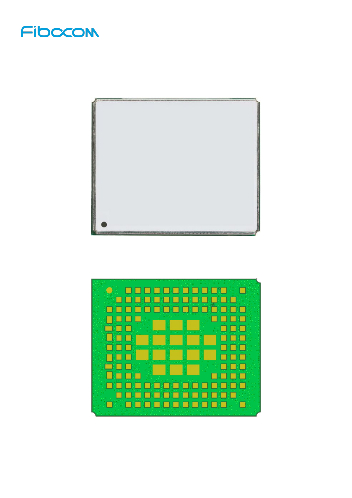
2.3 Appearance
Top View:
Figure 2- 1 Top View
Bottom view:
Figure 2- 2 Bottom View
L811-EA
L811-EA Module Hardware User Manual Page
14
of
43
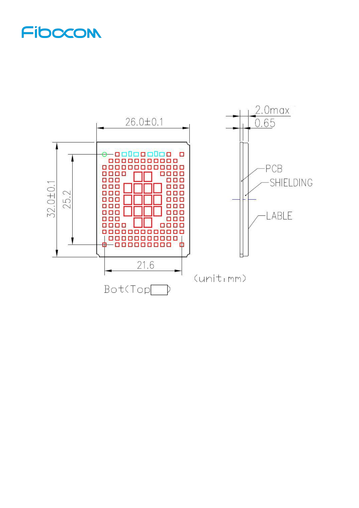
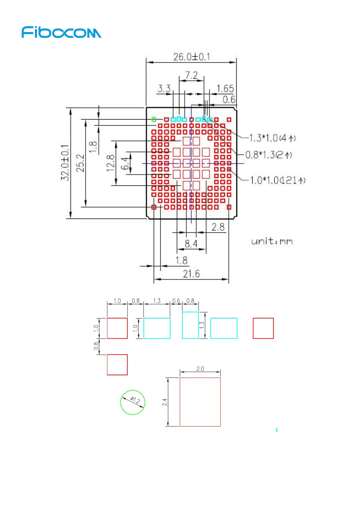
3 Structure
3.1 Dimension Diagram of Structure
Figure 3- 1 Dimension Diagram of Structure
L811-EA Module Hardware User Manual Page
16
of
43
Figure 3- 3 Structure Diagram of PCB Layout
L811-EA Module Hardware User Manual Page
17
of
43
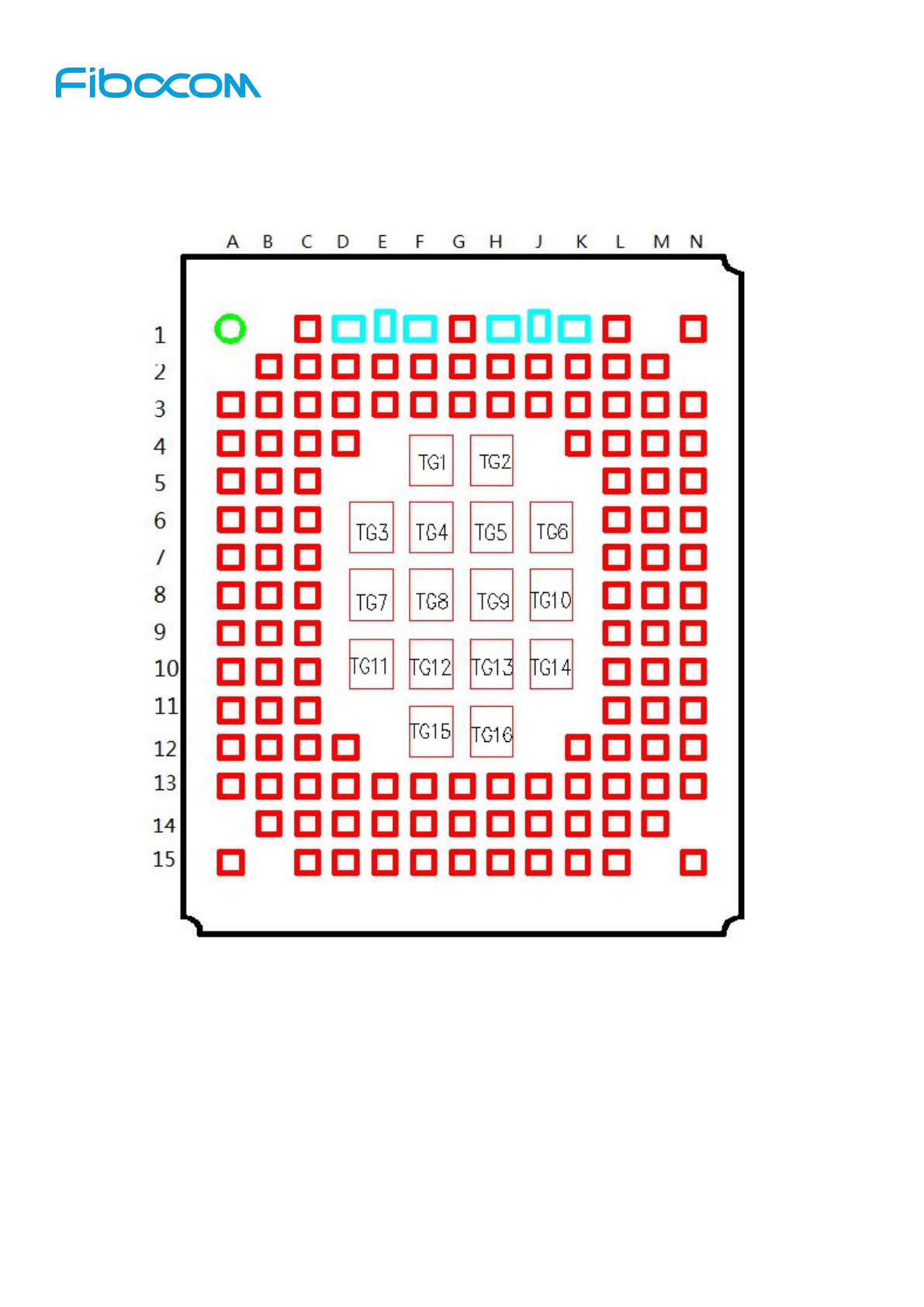
4 Hardware Introduction
4.1 Pin Definition
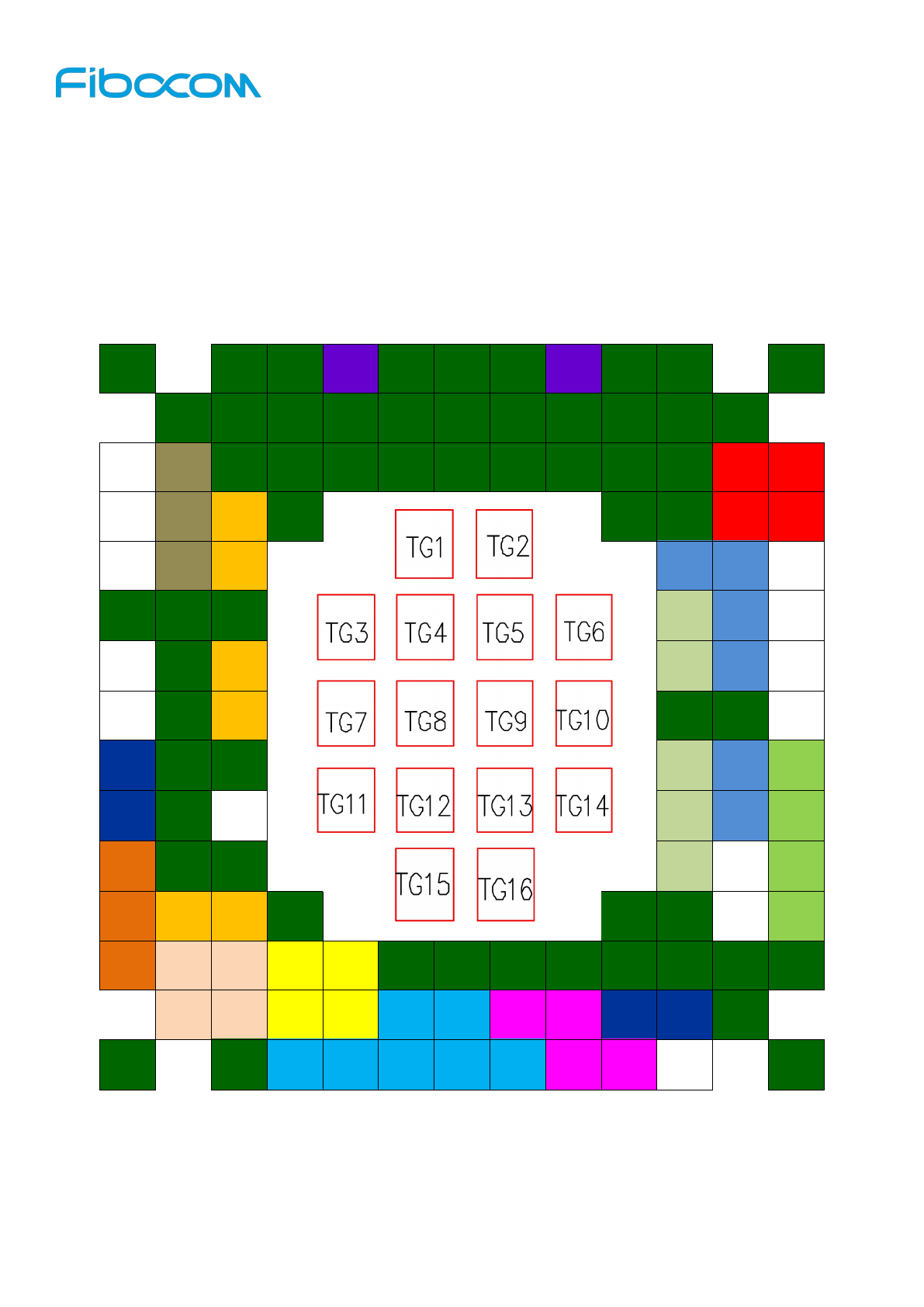
4.1.1 Pin Map
A
B
C
D
E
F
G
H
J
K
L
M
N
1
GND
GND
GND
ANT_DI
V
GND
GND
GND
ANT_MA
IN
GND
GND
GND
1
2
GND
GND
GND
GND
GND
GND
GND
GND
GND
GND
GND
2
3
FSYS2_
26M
RFE_RF
FE1_VIO
GND
GND
GND
GND
GND
GND
GND
GND
GND
VBAT
VBAT
3
4
CORE_D
UMP
RFE_RF
FE1_SC
LK
IPC_HO
ST_WA
KEUP
GND
GND
GND
VBAT
VBAT
4
5
LPG
RFE_RF
FE1_SD
ATA
IPC_TRI
G_OUT
TDO
TRST_N
VRTC
5
6
GND
GND
GND
HW_MO
N17
(TRC_D
ATA0)
TRIG_IN
VSD2_1
V8
6
7
WAKEU
P_HOST
GND
IPC_TRI
G_IN
HW_MO
N18
(TRC_C
LK)
TMS
RESET_
N
7
8
CLK32K
GND
IPC_SL
AVE_W
AKEUP
GND
GND
PWR_O
N/OFF#
8
9
UART1_
TXD
GND
GND
HW_MO
N19
(TRC_D
ATA1)
TCK
I2S2_W
A
9
10
UART1_
RXD
GND
NC
HW_MO
N20
(TRC_D
ATA2)
TDI
I2S2_TX
10
11
VBUS
GND
GND
HW_MO
N21
(TRC_D
ATA3)
I2C_SD
A
I2S2_RX
11
12
USB_DN
USB_HS
IC_STR
B
USB_HS
IC_DAT
A
GND
GND
GND
I2C_SCL
I2S2_CL
K
12
13
USB_DP
NC
NC
NC
NC
GND
GND
GND
GND
GND
GND
GND
GND
13
14
NC
NC
NC
NC
SIM1_D
P
SIM1_D
N
EINT3
BODY_S
AR
UART1_
RTS
UART1_
CTS
GND
14
15
GND
GND
VSIM1
SIM1_R
ST
SIM1_C
LK
SIM1_D
ATA
SIM1_C
D
WAKEU
P
W_DISA
BLE#
PA_BLA
NKING/T
RIG_OU
T
GND
15
A
B
C
D
E
F
G
H
J
K
L
M
N
Figure 4-2 Pins Definition
L811-EA Module Hardware User Manual Page
18
of
43
4.1.2 Description of Pins
The logic signal level of L811-EA module is 1.8V.
Pin#
Pin Name
I/O
Reset
Value
Idle
Value
Description
Power
N3
VBAT
PI
Power input
N4
VBAT
PI
Power input
M3
VBAT
PI
Power input
M4
VBAT
PI
Power input
N5
VRTC
PO
VRTC output
N6
VSD2_1V8
PO
VSD2_1V8 output
POWER_ON/OFF#,RESET
N7
RESET_N
I
Module reset input, pull up(100K ohms),1.8V
N8
POWER_ON/OFF#
I
Module power on/off signal, pull down (200K
ohms),1.8V
I2S
N9
I2S2_WA
O
PD
T
I2S LRCK,CMOS 1.8V
N10
I2S2_TX
O
PD
T
I2S data transmit, CMOS 1.8V
N11
I2S2_RX
I
PD
T
I2S data receive, CMOS 1.8V
N12
I2S2_CLK
O
PD
T
I2S serial clock, CMOS 1.8V
I2C
M11
I2C_SDA
IO
PU
PU
I2C serial data, pull up(4.7K ohms)CMOS
1.8V
M12
I2C_SCL
O
PU
PU
I2C serial clock, pull up(4.7K ohms)CMOS
1.8V
Clock
A3
FSYS2_26M
O
26MHz clock output,1.8V
A8
CLK32K
O
PD
PD
32kHz clock output,1.8V
SIM1
D15
VSIM1
PO
SIM1 power supply,1.8V/2.8V
E15
SIM1_RST
O
L
SIM1 reset
F15
SIM1_CLK
O
L
SIM1 clock
L811-EA Module Hardware User Manual Page
19
of
43
G15
SIM1_DATA
IO
L
SIM1 data, internal 4.7K resistor pull up
H15
SIM1_CD
I
T
SIM1 detect, pull up(390K ohms)CMOS 1.8V
F14
SIM1_DP
IO
PD
USB data plus for SIM1 card
G14
SIM1_DN
IO
PD
USB data minus for SIM1 card
USB2.0
A11
VBUS
PI
USB VBUS Supply
A12
USB_DN
IO
T
USB Data Minus
A13
USB_DP
IO
T
USB Data Plus
USB3.0
C13
NC
B13
NC
C14
NC
B14
NC
HSIC
B12
USB_HSIC_STRB
IO
High speed Inter IC clock (not supported
now)
C12
USB_HSIC_DATA
IO
High speed Inter IC data (not supported now)
C4
IPC_HOST_WAKEU
P
O
PU
H
IPC host wakeup (not supported now)
C5
IPC_TRIG_OUT
O
PD
L
IPC trig out (not supported now)
C7
IPC_TRIG_IN
I
PU
PU
IPC trig in (not supported now)
C8
IPC_SLAVE_WAKEU
P
I
PD
IPC slave wake up (not supported now)
SSIC
D14
NC
E14
NC
D13
NC
E13
NC
UART1
A9
UART1_TXD
O
PU
PP
UART1 transmit Data, CMOS 1.8V
A10
UART1_RXD
I
PD
PU
UART1 receive Data, CMOS 1.8V
K14
UART1_RTS
O
PU
PP
UART1 Request To Send, CMOS 1.8V
L811-EA Module Hardware User Manual Page
20
of
43
L14
UART1_CTS
I
PU
PU
UART1 Clear To Send, CMOS 1.8V
EINT
J15
WAKEUP
I
PD
PU
WAKEUP,CMOS 1.8V
K15
W_DISABLE#
I
PD
PU
W_DISABLE#,CMOS 1.8V
H14
EINT3
I
PD
PU
EINT3,CMOS 1.8V
J14
BODY_SAR
I
PU
PU
BODY_SAR,CMOS 1.8V
System status indicator
A4
CORE_DUMP
O
PD
L
Core dump indicator, CMOS 1.8V
A5
LPG
O
PD
LPG,CMOS 1.8V
A7
WAKEUP_HOST
O
PD
L
WAKEUP_HOST,CMOS 1.8V
L15
PA_BLANKING/
TRIG_OUT(T_OUT1)
O
PD
L
PA blanking output/Monitoring Signal Output,
CMOS 1.8V
ADC
C10
NC
JTAG
L5
TDO
O
T
Serial Data Out
M10
TDI
I
PU
Serial Data Input
M7
TMS
I
PU
State machine control signal
M9
TCK
I
PD
JTAG clock input
M5
TRST_N
I
PD
Reset/Module enable
M6
TRIG_IN
I
PD
Monitoring Signal Input, CMOS 1.8V
MIPI2 Trace
L7
MIPI2_TRC_CLK
O
PD
PP
MIPI2 trace clock, CMOS 1.8V
L6
MIPI2_TRC_DATA0
IO
PD
PP
MIPI2 trace data0,CMOS 1.8V
L9
MIPI2_TRC_DATA1
IO
PD
PP
MIPI2 trace data1,CMOS 1.8V
L10
MIPI2_TRC_DATA2
IO
PD
PP
MIPI2 trace data2,CMOS 1.8V
L11
MIPI2_TRC_DATA3
IO
PD
PP
MIPI2 trace data3,CMOS 1.8V
ANT Tunable
B5
RFE_RFFE1_SDATA
IO
PP
RFFE1 serial data for tunable ANT,CMOS
1.8V
B4
RFE_RFFE1_SCLK
O
PP
RFFE1 serial clock for tunable ANT,CMOS
1.8V
L811-EA Module Hardware User Manual Page
21
of
43
B3
RFE_RFFE1_VIO
PO
RFFE1 VIO for tunable ANT,1.8V
ANT
J1
ANT_MAIN
IO
Main antenna
E1
ANT_DIV
I
Diversity antenna
B8
GND
GND
B9
GND
GND
B10
GND
GND
B11
GND
GND
C11
GND
GND
F13
GND
GND
L12
GND
GND
M13
GND
GND
L13
GND
GND
G13
GND
GND
H13
GND
GND
J13
GND
GND
K13
GND
GND
A6
GND
GND
B2
GND
GND
B6
GND
GND
B7
GND
GND
C1
GND
GND
C2
GND
GND
C3
GND
GND
C6
GND
GND
C9
GND
GND
C15
GND
GND
D1
GND
GND
D2
GND
GND
D3
GND
GND
D4
GND
GND
L811-EA Module Hardware User Manual Page
22
of
43
D12
GND
GND
E2
GND
GND
E3
GND
GND
F1
GND
GND
F2
GND
GND
F3
GND
GND
G1
GND
GND
G2
GND
GND
G3
GND
GND
H1
GND
GND
H2
GND
GND
H3
GND
GND
J2
GND
GND
J3
GND
GND
K1
GND
GND
K2
GND
GND
K3
GND
GND
K4
GND
GND
K12
GND
GND
L1
GND
GND
L2
GND
GND
L3
GND
GND
L4
GND
GND
L8
GND
GND
M2
GND
GND
M8
GND
GND
M14
GND
GND
N13
GND
GND
A1
GND
GND
A15
GND
GND
N1
GND
GND
L811-EA Module Hardware User Manual Page
23
of
43
N15
GND
GND
TG1
GND
GND
TG2
GND
GND
TG3
GND
GND
TG4
GND
GND
TG5
GND
GND
TG6
GND
GND
TG7
GND
GND
TG8
GND
GND
TG9
GND
GND
TG10
GND
GND
TG11
GND
GND
TG12
GND
GND
TG13
GND
GND
TG14
GND
GND
TG15
GND
GND
TG16
GND
GND
H:High Voltage Level
L:Low Voltage Level
PD:Pull-Down
PU:Pull-Up
T:Tristate
OD:Open Drain
PP:Push-Pull
Note : The unused pins can be left floating in case of circuit design.
L811-EA Module Hardware User Manual Page
24
of
43
5 Hardware Interface
5.1 Power Interface
5.1.1 Power Supply
The L811-EA module requires a 3.3V - 4.5V DC power supply that capable of supplying maximum GSM
emission current which may up to 2A.
Input power supply requirements:
Parameter
Minimum Value
Recommended Value
Maximum Value
Unit
VBAT
3.3
3.8
4.4
V
Important notes for the power supply:
1. Voltage fluctuation of the power supply should be lower than 200mV.
2. VBAT should not lower than 3.3V when the voltage dropping occurs.
The filtering capacitors for designing the power supply as shown in the following tables:
Recommended
capacitance
Application
Description
330uF
Power supply
Reduce voltage fluctuation during the phone call.
For capacitance value, the bigger the better.
1uF,100nF
Digital signal noise
Filter for the interference caused by clock and
digital signals.
39pF,33pF
700 /850 /900 MHz
Filter for RF interference.
18pF,8.2pF,6.8pF
1700/1800/1900,
2100/2600MHz
Filter for RF interference.
5.1.2 VSD2_1V8
VSD2_1V8 is the power source of the internal digital circuits, it can be also used as the power indicator
and the reference voltage. For circuit design, it can be only used for low current application (<50mA),
floating if not used.
L811-EA Module Hardware User Manual Page
25
of
43
Parameters
Minimum Value
Typical Value
Maximum Value
Unit
VSD2_1V8
1.7135
1.8
1.8865
V
VIH
0.7* VSD2_1V8
1.8
1.8865
V
VIL
-0.3
0
0.3* VSD2_1V8
V
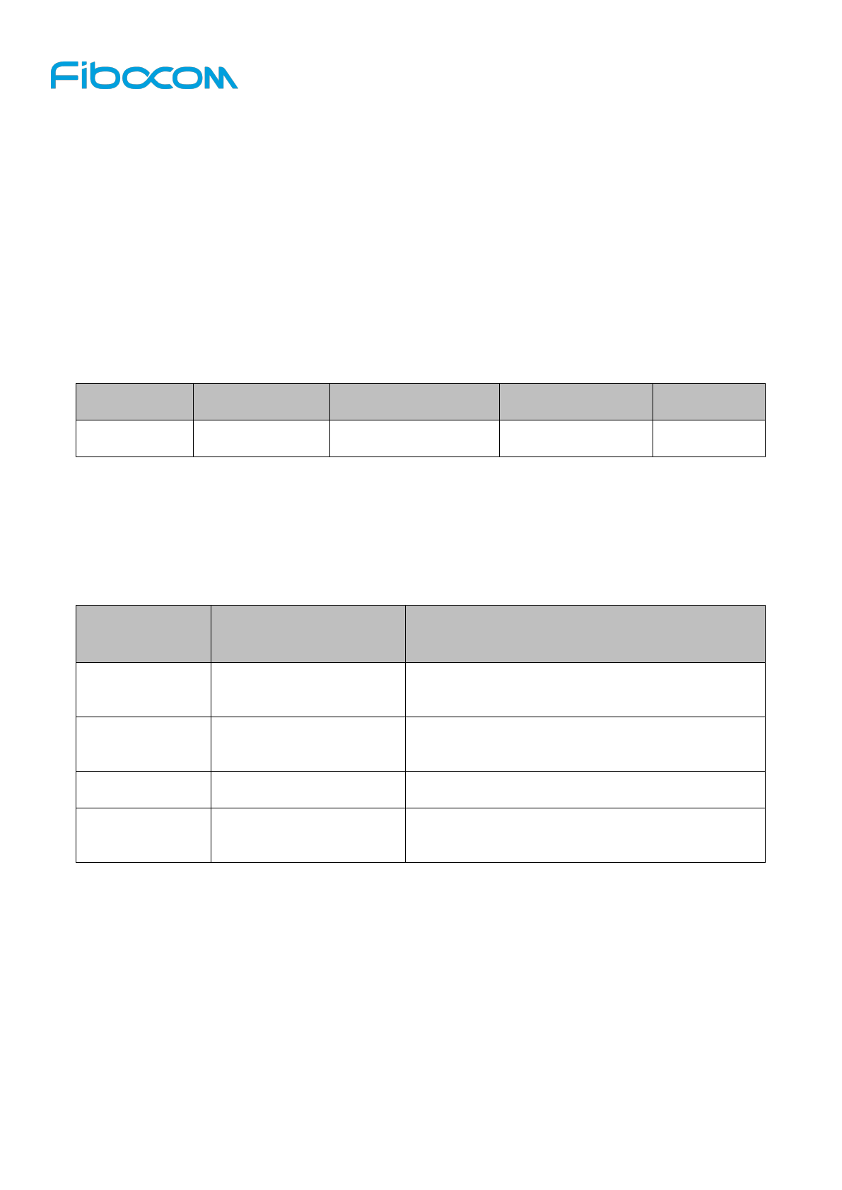
5.1.3 VRTC
VRTC is the power supply for the internal RTC of the module. In order to let RTC work for a certain time
when lost the VBAT power, as the backup power, it is recommended to add a big capacitor at the VRTC
pin.
The voltage range of the VRTC as shown in the following tables:
Parameters
Minimum Value
Recommended Value
Maximum Value
Unit
RTC working voltage
0.4
1.8
1.89
V
Voltage of VRTC
RTC Current Consumption
0.4V ~ 1V
1 uA
1V ~ 1.89V
2 uA
The reference design of VRTC circuit shown as follows:
Figure 5- 1 VRTC Reference Design
Note:
R8 is a current-limiting resistor, used to ensure the VRTC works properly and free from being affected
by peripheral circuits. R8 ≥ 1k Ohm.
The current consumption is about 2A when 1.8V VRTC is supplied from the external capacitor.
The value of C9 will affect the retaining time of RTC after VBAT is lost. The remaining time of RTC
can be roughly calculated by the following formula:
L811-EA Module Hardware User Manual Page
26
of
43
(1.8-1)*C/2 + (1-0.4)*C/1 = 0.4C + 0.6C = 1C
Ex.
When using a 100uF capacitor, the remaining time is 1*100 = 100 Sec.
When using a 330uF capacitor, the remaining time is 1*330 = 330 Sec.
If the RTC backup power function is not required, the VRTC pin can be left floating.
5.2 Power on/off and Reset Signal
The L811-EA module provides two control signals for power on/off and reset functions.
Pin definition as shown in the following tables:
Pin#
Pin Name
Electrical Level
Description
N8
POWER_ON/OFF#
CMOS 1.8V
Power on/off signal
N7
RESET_N
CMOS 1.8V
External reset signal input, active low.
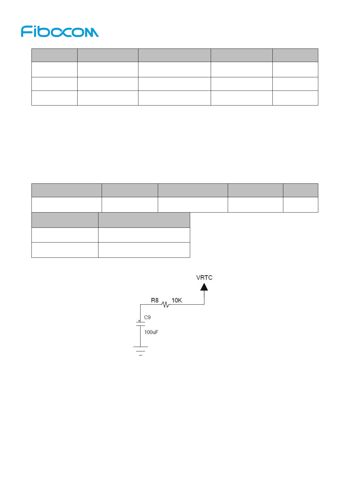
5.2.1 Power on /off Signal
5.2.1.1 Power on
After the power is applied to the module, pull up the POWER_ON/OFF# signal for at least 20ms then the
module will boot up.
The timing sequence diagram as follows:
Figure 5- 2 Power on Timing Control Diagram
Note :
The “>1s” time starts from the external capacitor being charged when the power is applied to the module.
If VBAT is already applied to the module then the time can be ignored, and AP(Application Processor)
L811-EA Module Hardware User Manual Page
27
of
43
only needs to control the timing of RESET_N and POWER_ON/OFF# signals.
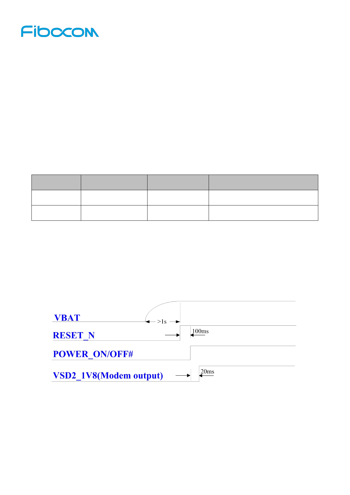
5.2.1.2 Power off
The L811-EA module can be turned off by software or hardware control. Software control is preferred for
normal cases, only when software control is not usable, then use the hardware control. By pulling down or
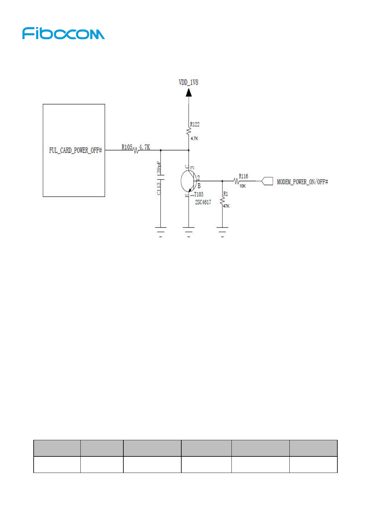
float the POWER_ON/OFF# signal, the module will be shut down. ①
For details as shown in the following tables:
Control Method
Action
Condition
Software
AT+CPWROFF
Normal control for power off.
Hardware
Pull down or floating the
POWER_ON/OFF#
signal.
Only used when a hardware exception occurs and
the software control cannot be used.
The hardware control description:
By pulling down or float the POWER_ON/OFF# signal, the PMU (Power Management Unit) of the module
will be reset, which results in the state changes from the working state to the shutdown state.
The timing sequence diagram as follows:
Figure 5- 3 Power off Timing Sequence Diagram
Note ①: To safely shut down the module, the RESET_N signal must be pulled down (for at least 100ms)
before pulling down the POWER_ON/OFF# signal.
L811-EA Module Hardware User Manual Page
28
of
43
5.2.1.3 The Recommended Design of Power on/off
The recommended design of POWER_ON/ OFF# signal is as follows:
Figure 5- 4 Recommended Design of POWER_ON/OFF# Signal
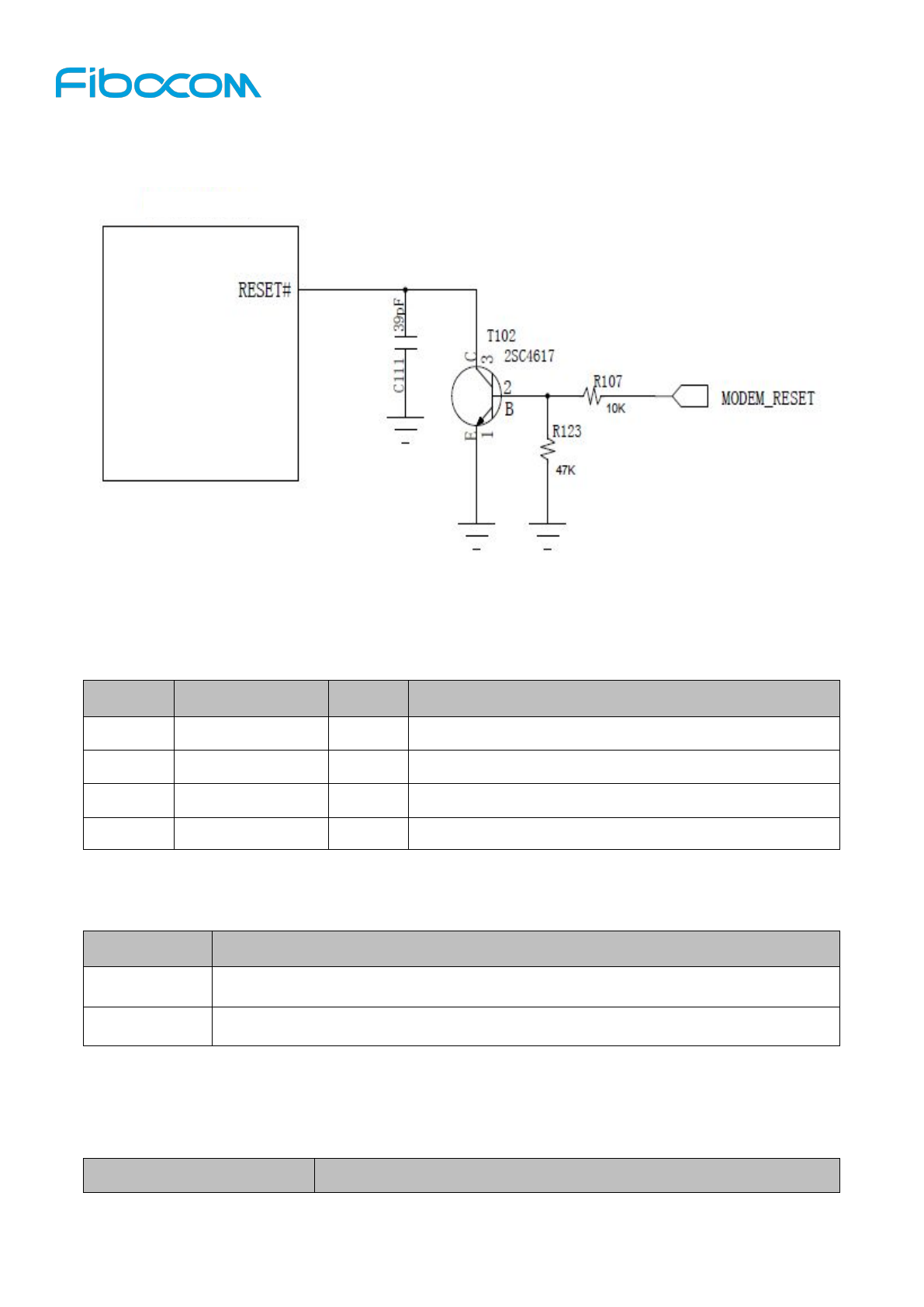
5.2.2 RESET Signal
The L811-EA module supports the external reset function. By controlling the RESET_N signal, the module
will reset to its initial state. When pulling down the RESET_N signal for 100ms, the module will be reset
and restarted. If the module is already turned on and working before the reset, there is no need to control
POWER_ON/OFF# signal to turn it on. PMU inside the module remains its power during the reset
procedure.
Note:
The reset signal is very sensitive. It should be kept away from RF interference and well wrapped with
ground planes in case of PCB layout. It is recommended to add a filter capacitor close to the module. Also,
RESET_N signal trace shall neither near the PCB edge nor route on the surface planes to avoid module
from reset caused by ESD.
The timing sequence requirement as follows:
Parameter
Condition
Minimum Value
Typical Value
Maximum Value
Unit
Pulse Width
Reset
7
100
1000
ms
L811-EA
L811-EA Module Hardware User Manual Page
29
of
43
Recommended design:
Figure 5- 5 Recommended Design of Reset Circuit
5.3 Status Indicating Signals
Pin#
Pin Name
I/O
Description
A4
CORE_DUMP
O
Core Dump Indicator
A5
LPG
O
LPG status Indicating
A7
WAKEUP_HOST
O
The module wakes up the host (Application processor).
L15
PA_BLANKING
O
PA Blanking output, external GPS control signal.
5.3.1 CORE DUMP Indicating
The CORE_DUMP signal is used to indicate the mode of the module.
Status
Mode
Normal mode
Low level
Core Dump
High level
5.3.2 LPG Signal
The LPG signal timing description as shown in the following tables:
Operating Modes
LPG signal
L811-EA
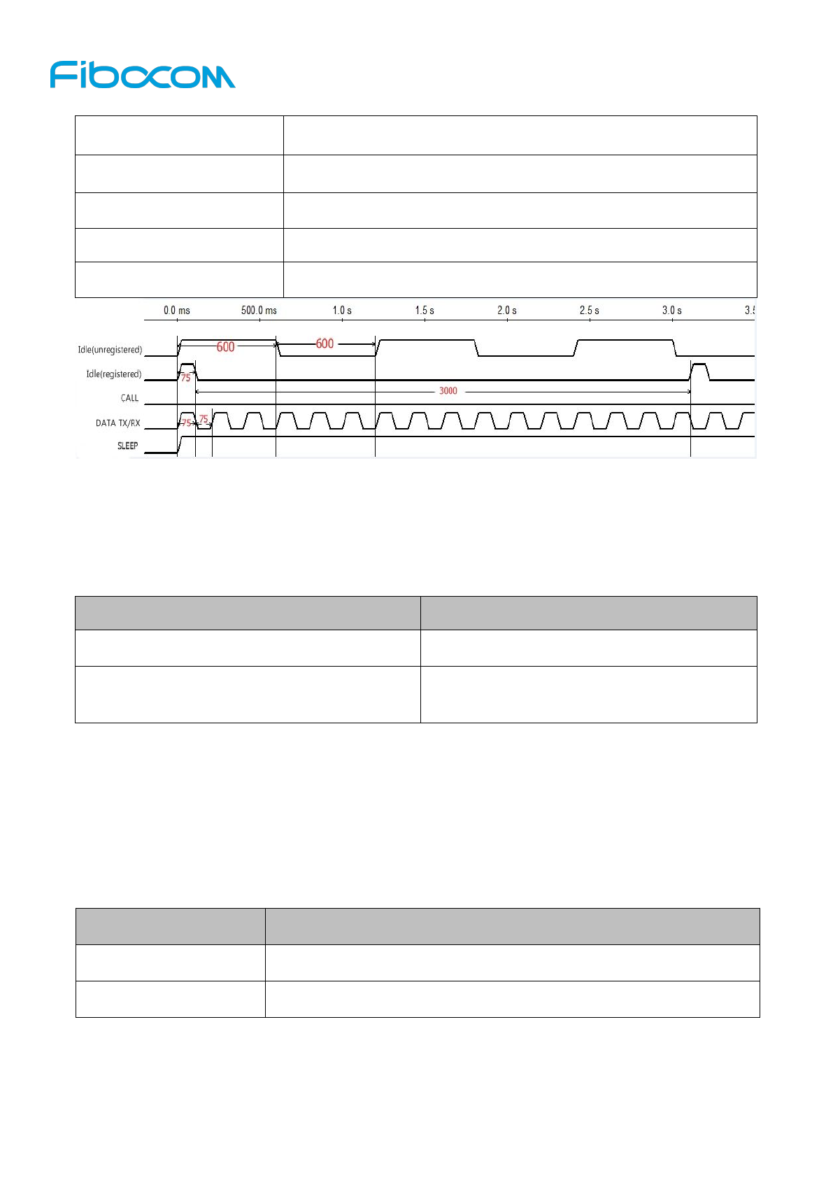
L811-EA Module Hardware User Manual Page
30
of
43
Idle (unregistered)
600ms high level and 600ms low level
Idle (registered)
75ms high level and 3s low level
Voice communication (Call)
Always low level
Data communication
75ms high level and 75ms low level
Sleep (sleep mode)
Always high level
5.3.3 WAKEUP_HOST Signal
The WAKEUP_HOST signal is used to wake up the host when there are incoming calls, SMS or other
data requests.
Status
WAKEUP_HOST Signal
Default
High level
Waking HOST(telephone ringing/SMS/other data
request)
Low level
5.3.4 PA_BLANKING Signal
The default is low for the signal. While the module works in GSM frequency band, PA_BLANKING will
output the pulses that synchronized with the GSM burst timing sequence.
Due to the GSM TX may interfere the receiving of the GPS signal, AP can turn off GPS or stop receiving
data from the GPS when it detecting the PA_BLANKING pulses.
Operating modes
PA_BLANKING Signal
Default modes
Low level
GSM TX
Output the pulse signal that synchronize with the GSM burst
L811-EA Module Hardware User Manual Page
31
of
43
5.4 Interrupt Control Signal
The interrupt control signals as shown in the following tables:
Pin#
Name
I/O
Description
J15
WAKEUP
I
Wake up the module.
K15
W_DISABLE#
I
Enable/Disable RF network.
H14
EINT3
I
Android & Linux/Win8 & Win10 dual
systems switch.
J14
BODY_SAR
I
Body SAR detection.
5.4.1 WAKE_UP Signal
WAKE_UP signal description as shown in the following tables:
Module Mode
WAKE_UP Signal
Description
Sleep
Low level
Wake up the module from Sleep to Idle mode
High level
Keep the module in Sleep mode
Idle/Call
Low level
Keep the current mode
High level
The module will not enter Sleep mode
5.4.2 W_DISABLE# Signal
The module provides a hardware signal to enable/disable WWAN RF function, it can be controlled by an
AT command also. The module will enter the Airplane mode by disabling RF function.
The definition of W_DISABLE# signal as shown in the following tables:
5.4.3 Android & Linux / Win8 & Win10 Dual Systems Switch
Control Signal
The L811-EA module supports Android & Linux / Win8 & Win10 dual systems switch by detecting the
voltage level of the interrupt signal EINT3.
The function of EINT3 signal as shown in the following tables:
No.
EINT3
Function
No.
W_DISABLE#
Function
1
Low
WWAN disabled, module enters Airplane mode.
2
High
WWAN enabled, module exits Airplane mode.
3
Floating
The WWAN function is defined by the AT command, enabled by default.
L811-EA Module Hardware User Manual Page
32
of
43
1
High/Floating
For Android or Linux system, the module`s USB ports mapped as 3*ACM
ports.
2
Low
For Win8 or Win10 system, the module`s USB port is mapped as a MBIM
mode.
Description:
1. During booting, the implementation of Android & Linux / Win8 & Win10 system change is done by
detecting the level of EINT3 signal. The voltage level of EINT3 should be kept stable during booting.
2. After boot up, the implementation of Android & Linux / Win8 & Win10 system change is done by
detecting the rising or falling edge of the EINT3 interrupt with the debounce time of 100ms. If the
interrupt event meets the condition, the module will restart and change over its USB mode for the
desired system.
5.5 USB Interface
5.5.1 USB Interface Definition
Pin#
Pin Name
I/O
Description
A13
USB_DP
I/O
USB D+ signal
A12
USB_DN
I/O
USB D- signal
A11
VBUS
I
USB power input
The L811-EA wireless communication module supports USB 2.0 interface. Before connecting it to the
Win7 system, it is necessary to install the USB driver (For Android & Linux system, no USB driver needed
but configuring the related kernel settings). After connecting the USB port to a PC, the USB driver resides
in the Windows system will map three ACM ports and four NCM ports, as listed below:
2 ACM ports used for AT Commands.
1 ACM ports used for LOG information captured by the debug software.
4 NCM ports are virtual network ports, mainly used for initiating data transmission serves.
Note:
One of the ACM ports can be used as a Modem COM port to initiate the data services. It is not
recommended to use due to the speed of Modem COM port is insufficient for the 100Mbps download
speed of the LTE standard. Only when the NCM ports are not available, the Modem COM port could
initiate the data service as the temporary solution.
L811-EA Module Hardware User Manual Page
33
of
43
5.5.2 USB Interface Application
Reference Circuit Design:
Figure 5- 6 USB Interface Reference Circuit Design
The choice of capacitance for RV101 and RV102 TVS diodes should not greater than 1pF, it is
recommended to use 0.5pF TVS diodes. There is no recommended capacitance value for RV100.
VUSB pin supplies the power for USB, the recommended power range is 3.3V ~ 4.5V. VBUS pin should
not floated or it will become the unknown device.
USB_DP and USB_DM are the high-speed differential signals, and the maximum data rate is 480Mbps.
The following requirements should be followed in case of PCB layout.
USB_DP and USB_DN signal traces should be parallel and have the equal length, avoid right angle
layout.
USB_DP and USB_DN signal traces should be wrapped with GND on both sides.
USB2.0 differential signal traces should be routed on the layer nearest to the ground plane.
Ensure the match of impedance, which is required to be 90 Ohm.
Note:
VBUS is the power for USB detection (it’s the low current signal, current value < 100uA). In circuit design,
it’s not permitted to apply VBUS power individually when the USB_DN and USB_DP are disconnected, or
the module will not go into the sleep mode.
5.6 UART Interface
5.6.1 UART Interface Description
The L811-EA module provides one 4-wire UART port. The UART1 port supports AT commands, the users
can receive and transmit AT commands through UART1.
L811-EA
L811-EA Module Hardware User Manual Page
34
of
43
The definition of UART1 signals as shown in the following tables:
Pin#
Pin Name
I/O
Description
L14
UART1_CTS
I
Clear to send
K14
UART1_RTS
O
Request to send
A9
UART1_TXD
O
Data Transmit
A10
UART1_RXD
I
Date Receive
5.6.2 UART Interface Application
The signal direction when connecting the UART1 of L811-EA module (DCE) and MCU (DTE) as shown in
the following tables:
MCU (DTE) application
Signal direction
L811-EA module (DCE)
RXD
UART1_TXD
TXD
UART1_RXD
Note:
The voltage level of UART interface is 1.8V. When connecting to 2.8V or 3.3V I/O, it is necessary to
convert the voltage level. In circuit design, it is recommended to use a SN74LVC2G07 to convert the
voltage level from 1.8V to 3.3V. For connecting to a PC, first convert 1.8V to 3.3V, then use a
SPIEX3232EEA to convert it to RS-232 level. The direction of the signals should be properly handled.
5.7 USIM Interface
The L811-EA module supports USIM and high speed SIM cards (The 8-wire USIM is not supported yet).
5.7.1 USIM Pins
Pin#
Pin Name
I/O
Function Description
D15
VSIM1
O
USIM power, 1.8V/2.8V
E15
SIM1_RST
O
USIM reset
F15
SIM1_CLK
O
USIM clock
G15
SIM1_DATA
I/O
USIM data
H15
SIM1_CD
I
USIM card detection signal, pulled up with a 390k
resistor by default.
High when SIM card is inserted.
Low when SIM card is not inserted.
L811-EA Module Hardware User Manual Page
35
of
43
5.7.2 USIM Interface Design
5.7.2.1 “Normally Closed” SIM Card Circuit Design
Reference Circuit Design::
Figure 5- 7 Reference Design of “Normally Closed” SIM Card Interface
Normally closed SIM Connector:
1)When detaching the SIM card, pin 7 and pin 8 shorted together.
2)When inserting the SIM card, pin 7 and pin 8 opened.
5.7.2.2 “Normally Open” SIM Circuit Design
Referenced Circuit Design:
Figure 5- 8 Reference Design of “Normally Open” SIM Card Interface
Normally open SIM Connector:
1)When detaching the SIM card, pin 7 and pin 8 opened .
2)When inserting the SIM card, pin 7 and pin 8 shorted.

L811-EA Module Hardware User Manual Page
36
of
43
Note:
In order to improve the EMC performance, the SIM card slot should be close to the module as much
as possible.
The filter capacitors for the SIM card signals should be placed close to the SIM card slot as much as
possible.
The ESD devices (e.g. TVS) shall be added to the SIM card signals for ESD protection. They should
be placed close to the SIM card slot as much as possible.
SIM1_CD signal supports hot-plugging. Active high by default (It can be changed to active low by an
AT command). If the module detects the signal with high level, it means a card insertion has detected.
5.7.3 Highlights for USIM Design
The SIM card interface design is very important to have the module and SIM card work normally.
The rules should be followed carefully as below:
SIM card slot and signal routing must keep away from the EMI interference sources, e.g. RF antenna
and digital signals.
The trace length between the module and SIM card should not exceed 100mm.
To avoid crosstalk, USIM_CLK and USIM_IO signals should keep away in case of layout. It’s
recommended to wrap them with ground planes.
SIM card signals should be ESD protected. The ESD devices should have low capacitance (e.g.
Zener diode). It’s recommended to choose ESD devices with capacitance equal or less than 33pF. In
case of layout, ESD devices should be close to the SIM card interface.
5.7.4 USIM Hot-Plugging
The L811-EA module supports the insert detection of the SIM card. With this function, the hot-plugging of
SIM card can be designed.
5.7.4.1 Hardware Connection
The function of SIM card hot-plugging is done by the SIM_CD signal. The SIM1_CD signal is low when
the SIM card is detached, high when the SIM card is inserted.
Note:
For “Normally closed” design, as shown in the figure5-7, the SIM1_CD signal is connected to U2’s
Pin8 (SW2), and Pin7 (SW1) is connected to the ground. When the SIM card is not inserted, SW2
and SW1 are shorted, and SW2 is low. When the SIM card is inserted, SW2 and SW1 are opened,
and the SIM1_CD signal will be pulled high.
For “Normally open” design, as shown in the figure5-8, the SIM1_CD signal is connected to U2’s Pin8
L811-EA Module Hardware User Manual Page
37
of
43
(SW2), and Pin7 (SW1) is pulled up with a 4.7K resistor. When the SIM card is not inserted, SW2 and
SW1 are opened, and SW2 is low. When the SIM card is inserted, SW2 and SW1 are shorted, and
SIM1_CD signal will be pulled high.
5.7.4.2 Software Setup
“+MSMPD” command is used for the SIM card detection function:
If set AT+MSMPD=0, the SIM card detection function is disabled, and the module will not detect the
SIM1_CD signal.
If set AT+MSMPD=1, the SIM card detection function is enabled, and the module will detect the
insertion of the SIM card via SIM1_CD Pin.
If SIM1_CD is high, which indicates the insertion of a SIM card, and the module will automatically
register to the network.
If SIM1_CD is low or disconnected, which indicates the SIM card is not inserted, and the module will
not register to the network.
Note:
The default value of +MSMPD is “1”. The SIM_CD signal is used for SIM card detection. The module
detects the presence of the SIM card via the SIM1_CD signal during the first booting. After the module
boots up, it detects the SIM card by the level change of the SIM1_CD signal. In other words, if SIM1_CD
is at low level, the module cannot access the SIM card.
5.8 Digital Audio
The L811-EA module supports I2S interface for digital audio. The I2S port supports normal I2S mode and
PCM mode for data transfer. I2S interface is at 1.8V voltage level.
I2S signal description as shown in the following tables:
Pin#
Pin Name
I/O
Description
N12
I2S2_CLK
O
Bit clock, 1.8V signal
N9
I2S2_WA0
O
Left and right channel clock (LRCK), 1.8V signal
N10
I2S2_TX
O
Serial data output, 1.8V signal
N11
I2S2_RX
I
Serial data input, 1.8V signal
5.8.1 I2S Interface
L811-EA
Signal Direction
Audio CODEC I2S Port
L811-EA Module Hardware User Manual Page
38
of
43
I2S2_CLK0
I2S_CLK
I2S2_WA0
I2S_LRCK
I2S2_RX
I2S_SDOUT
I2S2_TX
I2S_SDIN
Description:
I2S interface can be configured as master or slave mode.
It supports various audio sampling rates (48KHz, 44.1KHz, 32KHz, 24KHz, 22.5KHz, 16KHz, 12KHz,
11.025KHz and 8KHz).
5.8.2 PCM Mode Description
L811-EA
Signal Direction
Audio CODEC PCM Port
I2S2_CLK(PCM_CLK ,PCM clock signal)
PCM_CLK(PCM clock signal)
I2S2_WA(PCM_SYNC , PCM frame
synchronization signal)
PCM_SYNC(PCM frame
synchronization signal)
I2S2_RX(PCM_DIN , PCM data input)
PCM_DOUT(PCM data output)
I2S2_TX(PCM_DOUT , PCM data output)
PCM_DIN(PCM data input)
Note:
PCM port can be configured as master or slave mode.
It supports short frame sync for 16, 32, 48, and 64 bit mode.
It supports burst and continuous transmission modes.
It supports clock length trigger for frame sync signal and rising/falling edge trigger for data
transmission.
It supports various audio sampling rates (48KHz, 44.1KHz, 32KHz, 24KHz, 22.5KHz, 16KHz, 12KHz,
11.025KHz and 8KHz).
Note:
Because of the timing of I2S mode is simpler than PCM mode, it is recommended to use I2S mode for
audio transmission. For PCM mode, the audio quality issues caused by the PCM timing adjusting must be
avoided.
5.9 I2C Interface
L811-EA module supports one I2C interface, default configured as I2C master. The I2C master is used for
driving external I2C slave devices, such as audio codecs and so on.
L811-EA Module Hardware User Manual Page
39
of
43
Pin#
Name
I/O
Description
M11
I2C_DATA
I/O
I2C data signal,1.8V signal level
M12
I2C_SCL
O
I2C clock signal, 1.8V signal level
The signal connection of L811-EA I2C master and external I2C slave ( such as an audio codec)as shown
in the following tables:
L811-EA
Signal Direction
Audio Codec I2C Port
I2C_SDA
I2C_SDA
I2C_SCL
I2C_SCL
5.10 Clock Interface
L811-EA module supports one 26MHz clock output and one 32KHz clock output.
Pin#
Pin Name
I/O
Description
A3
FSYS2_26M
O
26MHz clock output, 1.8V level. (It is recommended to be
used for external GPS, and it can also be used for the main
clock of the audio codec)
A8
CLK32K
O
32K clock output, 1.8V level.
5.11 Other Interfaces
The module does not support the following ports yet: HSIC、ANT Tunable、GPIO.
L811-EA Module Hardware User Manual Page
40
of
43
6 Electrical and Environmental
Characteristic
6.1 Electrical Characteristic
The table below lists the range of L811-EA’s electrical characteristics:
Parameters
Minimum Value
Maximum Value
Unit
Power supply signal
0
4.4
V
Digital signal
0
1.9
V
6.2 Environmental Characteristic
This table below shows the environmental features of L811-EA.
Parameters
Minimum Value
Maximum Value
Unit
Operating Temperature
-40
+85
°C
Storage Temperature
-40
+85
°C
L811-EA Module Hardware User Manual Page
41
of
43
7 RF Interface
7.1 RF PCB Design
7.1.1 Wire Routing Principle
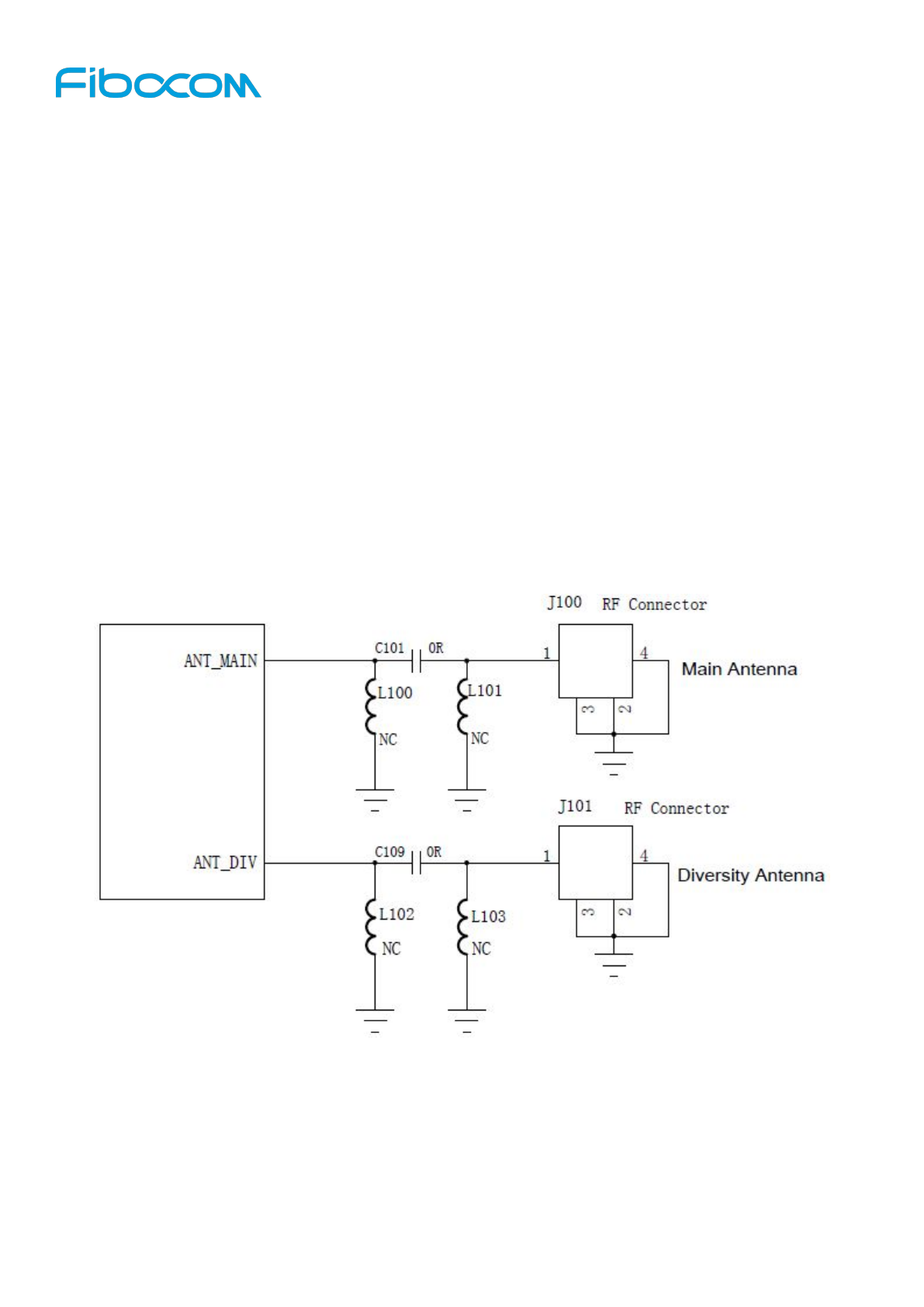
The L811-EA module supports double RF antennas, the MAIN_ANT is for transmitting and receiving, and
the DIV_ANT is for receiving. Diversity antenna can improve the receiver sensitivity as well as the
downlink speed.
The RF connectors or solder joints must be connected to the L811-EA module by the trace lines. It is
recommended to use the microstrip line for RF line. It should be as short as possible with the insertion
loss controlled below 0.2dB, and has the impedance of 50 Ohm.
For antenna fine tuning, it is recommended to reserve a π circuit (the parallel inductors should connect to
the main ground) between L811-EA module and the antenna connector (or the solder joint).
Figure 7- 1 L811-EA π-type Circuit
L811-EA

L811-EA Module Hardware User Manual Page
42
of
43
7.1.2 Impedance
The impedance of the RF signal line needs to be controlled at 50 Ohm.
7.2 Antenna Design
7.2.1 Main Antenna Design Requirements
(1) Antenna efficiency
Antenna efficiency is the ratio of the input power and radiant power. Because of the return loss, material
loss and coupling loss of the antenna, the radiant power is always lower than the input power. The ratio is
recommended to be controlled over 40% (–4dB).
(2) S11 or VSWR
S11 indicates the matching level of the 50 Ohm impedance for the antenna. It affects the antenna
efficiency in a certain extent. The VSWR testing method could be used for measuring purposes. The
recommended value for S11 is less than –10dB.
(3) Polarization
Polarization refers to the rotation direction of electric field while the antenna is in the direction of maximum
radiation. Linear polarization is recommended. It is recommended to use the diversity antenna which has
the different polarization direction from the main antenna.
(4) Radiation pattern
The radiation pattern refers to the intensity of the electromagnetic field while the antenna is in every
direction of the far field. Dipole antenna is perfect as the terminal antenna. For built-in antenna, it is
recommended to use PIFA or IFA antennas.
Antenna dimension: 6mm * 10mm * 100mm (H*W*L).
Antenna radiation direction: Omnidirectional.
(5) Gain and directivity
Antenna directivity refers to the intensity of the electromagnetic field while the electromagnetic wave is in
all directions. Gain is the collection of of the efficiency and directivity of the antenna. It is recommended
that antenna gain is less than or equal to 3dBi.
(6) Interference
In addition to antenna performance, some other interference from the PCB will also affect the module
performance. To ensure the high performance of the module, the interference must be under control.
Suggestions: Keep speaker, LCD, CPU, FPC wire routing, audio circuits, and power supply away from the

L811-EA Module Hardware User Manual Page
43
of
43
antenna, and add appropriate filtering and shielding protection, or adding filtering devices on the traces.
(7) TRP/TIS
TRP (Total Radiated Power):
GSM850/900>28dBm
GSM DCS1800/PCS1900 >25dBm
WCDMA Band 1,2,4,5,8>19dBm
LTE FDD Band 1,2,3,4,5,7,8,13,17,18,19,20>19dBm
TIS (Total Isotropic Sensitivity):
GSM850/900/DCS1800/PCS1900<-102dBm
WCDMA Band 1,2,4,5,8<-102dBm
LTE FDD Band 1,2,3,4,5,7,8,13,17,18,19,20<-95dBm (10MHz Bandwidth)