Fibocom Wireless L830EB LTE module User Manual
Fibocom Wireless Inc. LTE module
UserManual.wiki
>
Fibocom Wireless
>
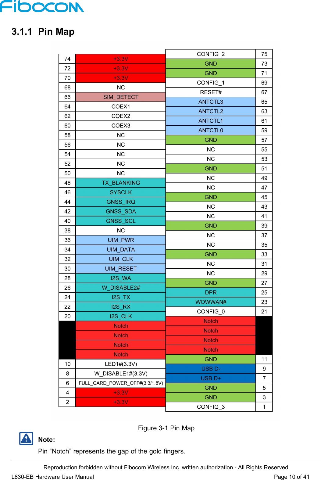
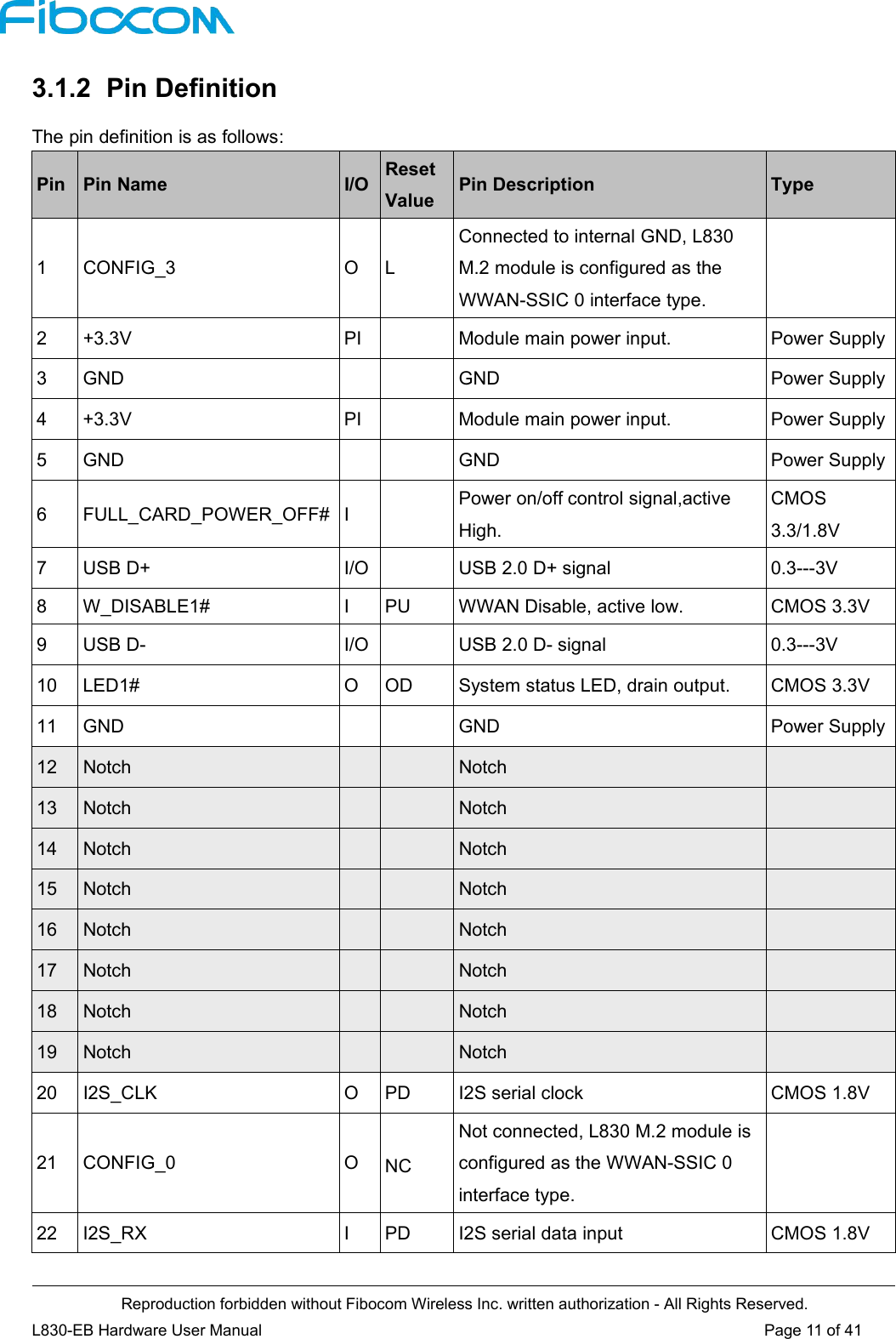
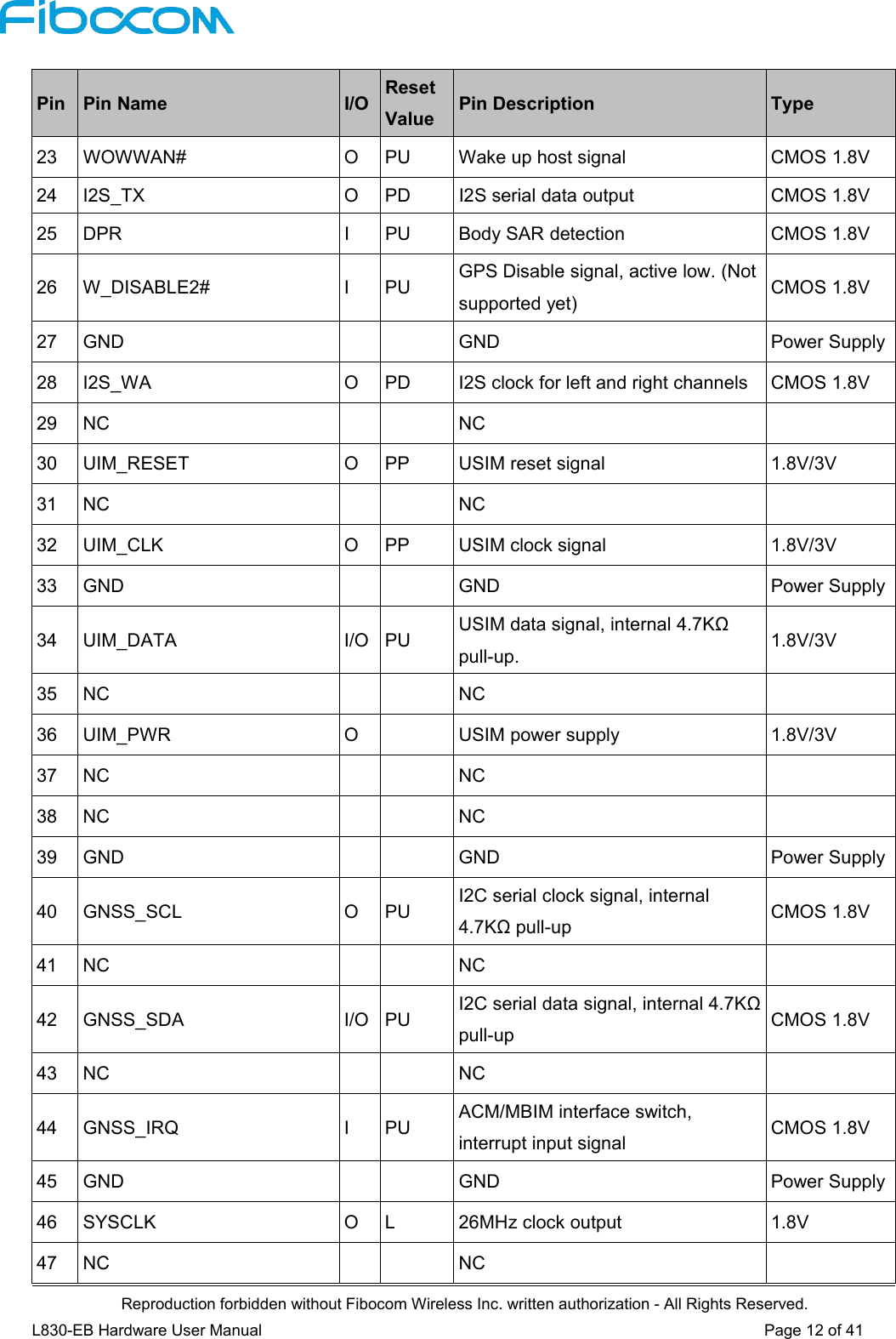
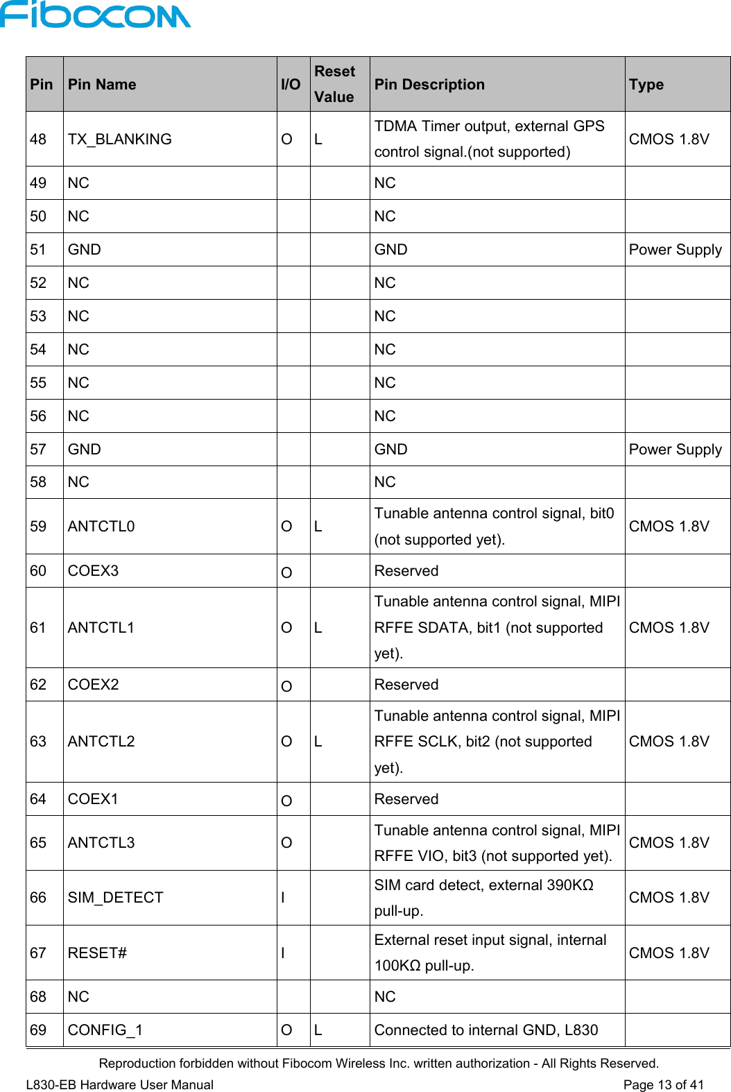
L830EB User Manual
User Manual
Navigation menu
Upload a User Manual
Namespaces
Wiki Guide
HTML
PDF
Info
Views
User Manual
Discussion / Help
Navigation