Fibocom Wireless L830EB LTE module User Manual
Fibocom Wireless Inc. LTE module
User Manual

Reproduction forbidden without Fibocom Wireless Inc. written authorization - All Rights Reserved.
L830-EBHardware User Manual Page
1
of
41
L830-EB Hardware User Manual
Lenovo Customization Version
Version: V1.0.0
Update date: 2017.07.04

Reproduction forbidden without Fibocom Wireless Inc. written authorization - All Rights Reserved.
L830-EB Hardware User Manual Page 2 of 41
Applicability Table
No. Product model Description
1 L830-EB-02 NA

Reproduction forbidden without Fibocom Wireless Inc. written authorization - All Rights Reserved.
L830-EB Hardware User Manual Page 3 of 41
Copyright
Copyright © 2017 Fibocom Wireless Inc. All rights reserved.
Without the prior written permission of the copyright holder, any company or individual is prohibited to
excerpt, copy any part of or the entire document, or distribute the document in any form.
Notice
The document is subject to update from time to time owing to the product version upgrade or other
reasons. Unless otherwise specified, the document only serves as the user guide. All the statements,
information and suggestions contained in the document do not constitute any explicit or implicit
guarantee.
Version Record
Version Update Remark
V1.0.0 2017-07-04 Initial version

Reproduction forbidden without Fibocom Wireless Inc. written authorization - All Rights Reserved.
L830-EB Hardware User Manual Page 4 of 41
Contents
1 Preface........................................................................................................................................... 6
1.1 Introduction........................................................................................................................................... 6
1.2 Reference Standard............................................................................................................................ 6
1.3 Related Documents............................................................................................................................. 6
2 Overview........................................................................................................................................7
2.1 Introduction........................................................................................................................................... 7
2.2 Specification..........................................................................................................................................7
2.3 Application Framework........................................................................................................................8
2.4 Hardware Framework..........................................................................................................................9
3 Application Interface.................................................................................................................. 9
3.1 M.2 Interface.........................................................................................................................................9
3.1.1 Pin Map............................................................................................................................................. 10
3.1.2 Pin Definition.....................................................................................................................................11
3.2 Power Supply..................................................................................................................................... 14
3.2.1 Power Supply................................................................................................................................... 15
3.2.2 Logic level......................................................................................................................................... 16
3.2.3 Power Consumption........................................................................................................................16
3.3 Control Signal.....................................................................................................................................17
3.3.1 Module Start-Up...............................................................................................................................17
3.3.1.1 Start-up Circuit................................................................................................................................................17
3.3.1.2 Start-up Timing Sequence............................................................................................................................ 18
3.3.2 Module Shutdown............................................................................................................................19
3.3.2.1 Software Shutdown........................................................................................................................................19
3.3.2.2 Hardware Shutdown...................................................................................................................................... 20
3.3.3 Module Reset................................................................................................................................... 21
3.4 USB Interface..................................................................................................................................... 22
3.4.1 USB Interface Definition................................................................................................................. 22
3.4.2 USB Interface Application.............................................................................................................. 22
3.5 USIM Interface................................................................................................................................... 23
3.5.1 USIM Pins......................................................................................................................................... 23
3.5.2 USIM Interface Circuit.....................................................................................................................23
3.5.2.1 N.C. SIM Card Slot........................................................................................................................................ 23
3.5.2.2 N.O. SIM Card Slot........................................................................................................................................ 24
3.5.3 USIM Hot-Plugging..........................................................................................................................25
3.5.4 USIM Design.................................................................................................................................... 25

Reproduction forbidden without Fibocom Wireless Inc. written authorization - All Rights Reserved.
L830-EB Hardware User Manual Page 5 of 41
3.6 Status Indicator.................................................................................................................................. 26
3.6.1 LED#1 Signal....................................................................................................................................26
3.6.2 WOWWAN#......................................................................................................................................27
3.7 Interrupt Control................................................................................................................................. 27
3.7.1 W_DISABLE1#.................................................................................................................................28
3.7.2 System Switch Control....................................................................................................................28
3.7.3 Body SAR..........................................................................................................................................28
3.8 Digital Audio........................................................................................................................................29
3.8.1 I2S Mode...........................................................................................................................................29
3.8.2 PCM Mode........................................................................................................................................ 30
3.9 I2C Interface Description..................................................................................................................30
3.10 Clock Interface................................................................................................................................. 31
3.11 Configuration Interface....................................................................................................................31
3.12 Other Interfaces............................................................................................................................... 32
4 Radio Frequency.......................................................................................................................32
4.1 RF Interface........................................................................................................................................32
4.1.1 RF Interface Functionality.............................................................................................................. 32
4.1.2 RF Connector Characteristic......................................................................................................... 32
4.1.3 RF Connector Dimension...............................................................................................................32
4.2 Operating Band.................................................................................................................................. 34
4.3 Transmitting Power............................................................................................................................34
4.4 Receiver Sensitivity........................................................................................................................... 35
4.5 GNSS...................................................................................................................................................35
4.6 Antenna Design..................................................................................................................................36
5 Structure Specification............................................................................................................37
5.1 Product Appearance..........................................................................................................................37
5.2 Dimension of Structure..................................................................................................................... 37
5.3 M.2 Interface Model...........................................................................................................................38
5.4 M.2 Connector....................................................................................................................................38
5.5 Storage................................................................................................................................................39
5.5.1 Storage Life...................................................................................................................................... 39
5.6 Packing................................................................................................................................................39
5.6.1 Tray Package....................................................................................................................................40
5.6.2 Tray size............................................................................................................................................ 41

Reproduction forbidden without Fibocom Wireless Inc. written authorization - All Rights Reserved.
L830-EB Hardware User Manual Page 6 of 41
1 Preface
1.1 Introduction
The document describes the electrical characteristics, RF performance, dimensions and application
environment, etc. of L830-EB (hereinafter referred to as L830). With the assistance of the document and
other instructions, the developers can quickly understand the hardware functions of L830 modules and
develop products.
1.2 Reference Standard
The design of the product complies with the following standards:
3GPP TS 34.121-1 V10.8.0: User Equipment (UE) conformance specification;Radio
transmission and reception (FDD);Part 1: Conformance specification
3GPP TS 36.521-1 V10.6.0: User Equipment (UE) conformance specification; Radio
transmission and reception; Part 1: Conformance testing
3GPP TS 21.111 V10.0.0: USIM and IC card requirements
3GPP TS 51.011 V4.15.0: Specification of the Subscriber Identity Module -Mobile Equipment
(SIM-ME) interface
3GPP TS 31.102 V10.11.0: Characteristics of the Universal Subscriber Identity Module (USIM)
application
3GPP TS 31.11 V10.16.0: Universal Subscriber Identity Module (USIM) Application
Toolkit(USAT)
3GPP TS 36.124 V10.3.0: ElectroMagnetic Compatibility (EMC) requirements for mobile
terminals and ancillary equipment
3GPP TS 27.007 V10.0.8: AT command set for User Equipment (UE)
PCI_Express_M.2_Specification_Rev1.1
1.3 Related Documents
RF Antenna Application Design Specification
L8-Family System Driver Integration and Application Guidance
L8-Family AT Commands Manual

RF_067, Issue 01
EU Regulator Conformance
Hereby, We, Fibocom Wireless Inc. declares that the radio equipment type L830-EB is in compliance
with the Directive 2014/53/EU.
In all cases assessment of the final product must be mass against the Essential requirements of the
Directive 2014/53/EU Article 3.1(a) and (b), safety and EMC respectively, as well as any relevant Article
3.2 requirements.
External antenna is used with the module during the testing process, the maximum antenna gain for
frequency < 1G is 3dBi, for frequency > 1G is 5dBi and the antenna separation distance is 20cm.
EU Declaration of Conformity (DoC)
Hereby,
Name of manufacturer: Fibocom Wireless Inc.
Address: 5/F, Tower A, Technology Building II, 1057 Nanhai Blvd,
Nanshan,
City: Shenzhen,
Country: China
declares that the DoC is issued under its sole responsibility and that this product:
Product description: LTE module
Type designation(s): L830-EB
Trademark: Fibocom
Product Identification
Element L830-EB
is in conformity with the relevant Union harmonization legislation:
Radio Equipment directive: 2014 / 53 / EU.
with reference to the following standards applied:
1. Health (Article 3.1(a) of Directive 2014/53/EU)
Applied Standard(s):
EN 62311 : 2008
2. Safety (Article 3.1(a) of Directive 2014/53/EU)
Applied Standard(s):
EN 60950-1: 2006 + A11: 2009 + A1: 2010 + A12: 2011 + A2: 2013
3. Electromagnetic compatibility (Article 3.1 (b) of Directive 2014/53/EU)
Applied Standard(s):
Draft EN 301 489-1 V2.2.0 / -52 V1.1.0 / Final Draft EN301489-3 V2.1.1
4. Radio frequency spectrum usage (Article 3.2 of Directive 2014/53/EU)
Applied Standard(s):
EN 301 908-1 V11.1.1 / -2 V11.1.1 / -13 V11.1.1
EN 303 413 V1.1.1
The Notified Body SIEMIC INC. with Notified Body number 2200 performed:
Modules: B+C and issued the EU-type examination certificate.
Signed for and on behalf of:
Date: August 21, 2017
City: Shenzhen,
Name: Bond Yuan
Title: Certification Engineer
Signature:
Federal Communication Commission Interference Statement
This device complies with Part 15 of the FCC Rules. Operation is subject to the following two
conditions: (1) This device may not cause harmful interference, and (2) this device must
accept any interference received, including interference that may cause undesired operation.
This equipment has been tested and found to comply with the limits for a Class B digital
device, pursuant to Part 15 of the FCC Rules. These limits are designed to provide
reasonable protection against harmful interference in a residential installation. This equipment
generates, uses and can radiate radio frequency energy and, if not installed and used in
accordance with the instructions, may cause harmful interference to radio communications.
However, there is no guarantee that interference will not occur in a particular installation. If
this equipment does cause harmful interference to radio or television reception, which can be
determined by turning the equipment off and on, the user is encouraged to try to correct the
interference by one of the following measures:
Reorient or relocate the receiving antenna.
Increase the separation between the equipment and receiver.
Connect the equipment into an outlet on a circuit different from that
to which the receiver is connected.
Consult the dealer or an experienced radio/TV technician for help.
FCC Caution:
Any changes or modifications not expressly approved by the party responsible for
compliance could void the user's authority to operate this equipment.
This transmitter must not be co-located or operating in conjunction with any other
antenna or transmitter.

Radiation Exposure Statement:
This equipment complies with FCC radiation exposure limits set forth for an uncontrolled
environment. This equipment should be installed and operated with minimum distance 20cm
between the radiator & your body.
This device is intended only for OEM integrators under the following conditions:
1)
2) The transmitter module may not be co-located with any other transmitter or antenna.
As long as 2 conditions above are met, further transmitter test will not be required. However,
the OEM integrator is still responsible for testing their end-product for any additional
compliance requirements required with this module installed
IMPORTANT NOTE: In the event that these conditions can not be met (for example certain
laptop configurations or co-location with another transmitter), then the FCC authorization is
no longer considered valid and the FCC ID can not be used on the final product. In these
circumstances, the OEM integrator will be responsible for re-evaluating the end product
(including the transmitter) and obtaining a separate FCC authorization.
End Product Labeling
This transmitter module is authorized only for use in device where the antenna may be
installed such that 20 cm may be maintained between the antenna and users. The final end
product must be labeled in a visible area with the following: Contains FCC ID:
The grantee's FCC ID can be used only when all FCC compliance requirements are met.
Manual Information To the End User
The OEM integrator has to be aware not to provide information to the end user regarding how
to install or remove this RF module in the user’s manual of the end product which integrates
this module. The end user manual shall include all required regulatory information/warning as
show in this manual.
ZMOL830EB
External antenna is used with the module during the testing process, the maximum antenna gain for
frequency<1G is 3dBi, for frequency>1G is 5 dBi and the antenna separation distance is 20cm.
Reproduction forbidden without Fibocom Wireless Inc. written authorization - All Rights Reserved.
L830-EB Hardware User Manual Page 7 of 41
2 Overview
2.1 Introduction
The L830 is a highly integrated 4G cellular module which uses the standard PCIe M.2 interface.It supports
LTE FDD/WCDMA mode cellular communication.
2.2 Specification
Specification
Operating Band
LTE FDD: Band 1,3,5,7,8,20,28
WCDMA/HSPA+: Band I, V, VIII
GPS/GLONASS: L1
CA
LTE inter-band CA
1 +3,5,7,20
3 +5,7,8,20,28
5 +7
7 +20,28
LTE intra-band CA 3,7
Data
Transmission
LTE FDD 300Mbps DL/50Mbps UL(Cat 6)
UMTS/HSPA+
UMTS:384 kbps DL/384 kbps UL
DC-HSDPA+:42Mbps DL(Cat 24)/5.76Mbps UL(Cat6)
Power Supply DC 3.135V~4.4V, Typical 3.3V
Temperature
Normal Operating temperature:-10°C ~+55°C
Extended Operating temperature:-30°C ~+65°C
Storage temperature:-40°C ~+85°C
Physical
characteristics
Interface: M.2 Key-B
Dimension:30 x 42 x 2.3mm
Weight: About 5.8 g
Interface
Antenna Connector
WWAN Main Antenna x 1
WWAN Diversity(GNSS AUX) Antenna x 1
WCDMA Band 1/8 24dBm
LTE Band 1/3/7/8/20 23dBm
Reproduction forbidden without Fibocom Wireless Inc. written authorization - All Rights Reserved.
L830-EB Hardware User Manual Page 8 of 41
Function Interface
USIM 3V/1.8V
USB 2.0 x 1
I2S
I2C
EINT、System Indicator
Clock
Software
Protocol Stack IPV4/IPV6
AT commands 3GPP TS 27.007 and 27.005, and proprietary FIBOCOM AT commands
Firmware update USB
Note:
When the temperature goes beyond the normal operating temperature range of -10°C~+55°C, the
RF performance of the module may be slightly off 3GPP specifications.
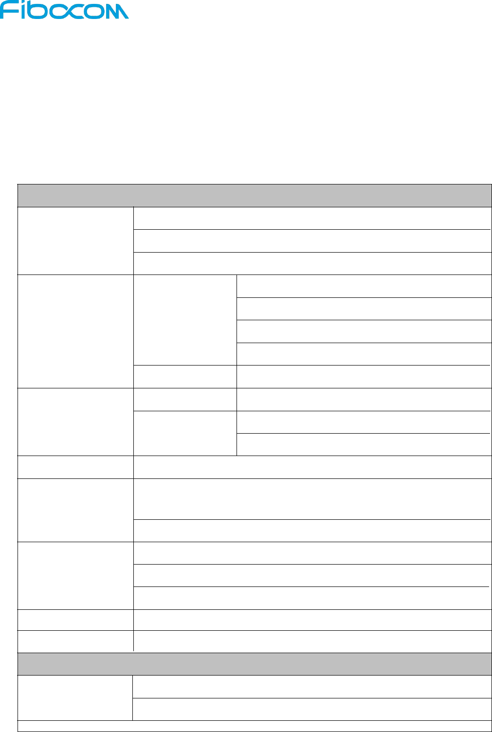
2.3 Application Framework
The peripheral applications for L830 module are shown in Figure 2-1:
Figure2-1 Application Framework
Reproduction forbidden without Fibocom Wireless Inc. written authorization - All Rights Reserved.
L830-EB Hardware User Manual Page 9 of 41
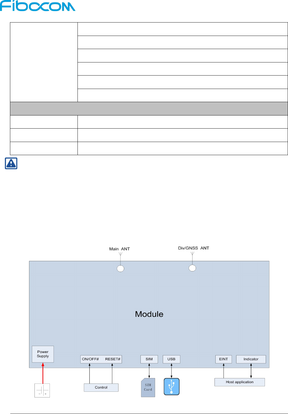
2.4 Hardware Framework
The hardware framework in Figure 2-2 shows the main hardware functions of L830 module, including
baseband and RF functions.
Baseband contains the followings:
UMTS/LTE FDD controller/Power supply
NAND/internal LPDDR2 RAM
Application interface
RF contains the followings:
RF Transceiver
RF Power/PA
RF Front end
RF Filter
Antenna Connector
Figure 2-2 Hardware Framework
3 Application Interface
3.1 M.2 Interface
The L830 module uses standard M.2 Key-B interface, with a total of 75 pins.
Reproduction forbidden without Fibocom Wireless Inc. written authorization - All Rights Reserved.
L830-EB Hardware User Manual Page 10 of 41
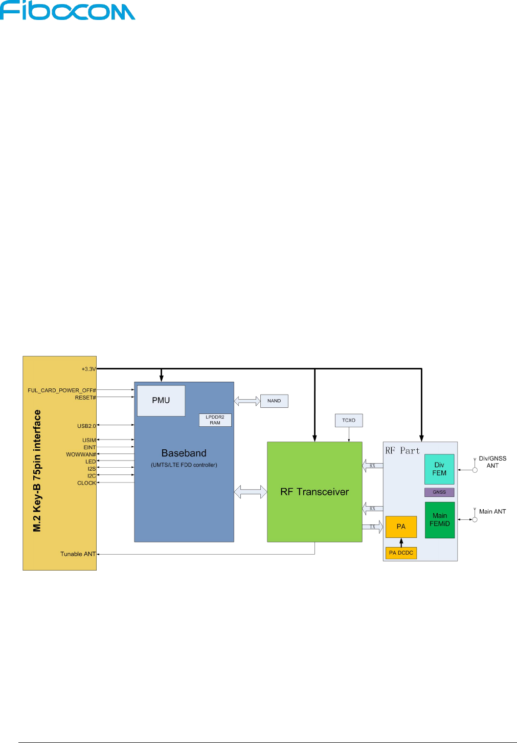
3.1.1 Pin Map
Figure 3-1 Pin Map
Note:
Pin “Notch” represents the gap of the gold fingers.

Reproduction forbidden without Fibocom Wireless Inc. written authorization - All Rights Reserved.
L830-EB Hardware User Manual Page 11 of 41
3.1.2 Pin Definition
The pin definition is as follows:
Pin Pin Name I/O Reset
Value Pin Description Type
1 CONFIG_3 O L
Connected to internal GND, L830
M.2 module is configured as the
WWAN-SSIC 0 interface type.
2 +3.3V PI Module main power input. Power Supply
3 GND GND Power Supply
4 +3.3V PI Module main power input. Power Supply
5 GND GND Power Supply
6 FULL_CARD_POWER_OFF# I Power on/off control signal,active
High.
CMOS
3.3/1.8V
7 USB D+ I/O USB 2.0 D+ signal 0.3---3V
8 W_DISABLE1# I PU WWAN Disable, active low. CMOS 3.3V
9 USB D- I/O USB 2.0 D- signal 0.3---3V
10 LED1# O OD System status LED, drain output. CMOS 3.3V
11 GND GND Power Supply
12 Notch Notch
13 Notch Notch
14 Notch Notch
15 Notch Notch
16 Notch Notch
17 Notch Notch
18 Notch Notch
19 Notch Notch
20 I2S_CLK O PD I2S serial clock CMOS 1.8V
21 CONFIG_0 O NC
Not connected, L830 M.2 module is
configured as the WWAN-SSIC 0
interface type.
22 I2S_RX I PD I2S serial data input CMOS 1.8V

Reproduction forbidden without Fibocom Wireless Inc. written authorization - All Rights Reserved.
L830-EB Hardware User Manual Page 12 of 41
Pin Pin Name I/O Reset
Value Pin Description Type
23 WOWWAN# O PU Wake up host signal CMOS 1.8V
24 I2S_TX O PD I2S serial data output CMOS 1.8V
25 DPR I PU Body SAR detection CMOS 1.8V
26 W_DISABLE2# I PU GPS Disable signal, active low. (Not
supported yet) CMOS 1.8V
27 GND GND Power Supply
28 I2S_WA O PD I2S clock for left and right channels CMOS 1.8V
29 NC NC
30 UIM_RESET O PP USIM reset signal 1.8V/3V
31 NC NC
32 UIM_CLK O PP USIM clock signal 1.8V/3V
33 GND GND Power Supply
34 UIM_DATA I/O PU USIM data signal, internal 4.7KΩ
pull-up. 1.8V/3V
35 NC NC
36 UIM_PWR O USIM power supply 1.8V/3V
37 NC NC
38 NC NC
39 GND GND Power Supply
40 GNSS_SCL O PU I2C serial clock signal, internal
4.7KΩ pull-up CMOS 1.8V
41 NC NC
42 GNSS_SDA I/O PU I2C serial data signal, internal 4.7KΩ
pull-up CMOS 1.8V
43 NC NC
44 GNSS_IRQ I PU ACM/MBIM interface switch,
interrupt input signal CMOS 1.8V
45 GND GND Power Supply
46 SYSCLK O L 26MHz clock output 1.8V
47 NC NC

Reproduction forbidden without Fibocom Wireless Inc. written authorization - All Rights Reserved.
L830-EB Hardware User Manual Page 13 of 41
Pin Pin Name I/O Reset
Value Pin Description Type
48 TX_BLANKING O L TDMA Timer output, external GPS
control signal.(not supported) CMOS 1.8V
49 NC NC
50 NC NC
51 GND GND Power Supply
52 NC NC
53 NC NC
54 NC NC
55 NC NC
56 NC NC
57 GND GND Power Supply
58 NC NC
59 ANTCTL0 O L Tunable antenna control signal, bit0
(not supported yet). CMOS 1.8V
60 COEX3 OReserved
61 ANTCTL1 O L
Tunable antenna control signal, MIPI
RFFE SDATA, bit1 (not supported
yet).
CMOS 1.8V
62 COEX2 OReserved
63 ANTCTL2 O L
Tunable antenna control signal, MIPI
RFFE SCLK, bit2 (not supported
yet).
CMOS 1.8V
64 COEX1 OReserved
65 ANTCTL3 O Tunable antenna control signal, MIPI
RFFE VIO, bit3 (not supported yet). CMOS 1.8V
66 SIM_DETECT I SIM card detect, external 390KΩ
pull-up. CMOS 1.8V
67 RESET# I External reset input signal, internal
100KΩ pull-up. CMOS 1.8V
68 NC NC
69 CONFIG_1 O L Connected to internal GND, L830
Reproduction forbidden without Fibocom Wireless Inc. written authorization - All Rights Reserved.
L830-EB Hardware User Manual Page 14 of 41
Pin Pin Name I/O Reset
Value Pin Description Type
M.2 module is configured as the
WWAN-SSIC 0 interface type.
70 +3.3V PI Module main power input. Power Supply
71 GND GND Power Supply
72 +3.3V PI Module main power input. Power Supply
73 GND GND Power Supply
74 +3.3V PI Module main power input. Power Supply
75 CONFIG_2 O L
Connected to internal GND, L830
M.2 module is configured as the
WWAN-SSIC 0 interface type.
Reset Value: The initial status after module reset, not the status when working
H: High Voltage Level
L: Low Voltage Level
PD: Pull-Down
PU: Pull-Up
T: Tristate
OD: Open Drain
PP: Push-Pull
PI: Power Input
PO: Power Output
Note:
The unused pins can be left floating.
3.2 Power Supply
The power interface of L830 module as shown in the following table:
Pin Pin Name I/O Pin Description
DC Parameter(V)
Minimum
Value
Typical
Value
Maximum
Value
2,4,70,72,74 +3.3V PI Power supply input 3.135 3.3 4.4
36 UIM_PWR PO USIM power supply 1.8V/3V
Reproduction forbidden without Fibocom Wireless Inc. written authorization - All Rights Reserved.
L830-EB Hardware User Manual Page 15 of 41
3.2.1 Power Supply
The L830 module should be powered through the +3.3V pins, and the power supply design is shown in
Figure 3-2:
Figure 3-2 Power Supply Design
The filter capacitor design for power supply as shown in the following table:
Recommended
capacitance Application Description
220uF x 2 Voltage-stabilizing capacitors
Reduce power fluctuations of the module in
operation, requiring capacitors with low ESR.
LDO or DC/DC power supply requires the
capacitor of no less than 220uF
The capacitor for battery power supply
can be reduced to 100uF
1uF,100nF Digital signal noise Filter out the interference generated from the
clock and digital signals
39pF,33pF
700/800, 850/900 MHz
frequency band
Filter out low frequency band RF interference
18pF,8.2pF,6.8pF 1800,2100,2600MHz frequency
band
Filter out medium/high frequency band RF
interference
The stable power supply can ensure the normal operation of L830 module; and the ripple of the power
supply should be less than 300mV in design. When the module operates with the maximum emission
power, the maximum operating current can reach 1A, so the power source should be not lower than
3.135V, or the module may shut down or reboot. The power supply limits are shown in Figure 3-3:
Reproduction forbidden without Fibocom Wireless Inc. written authorization - All Rights Reserved.
L830-EB Hardware User Manual Page 16 of 41
Figure 3-3 Power Supply Limit
3.2.2 Logic level
The L830 module 1.8V logic level definition as shown in the following table:
Parameters Minimum Typical Maximum Unit
1.8V logic level 1.71 1.8 1.89 V
VIH 1.3 1.8 1.89 V
VIL -0.3 0 0.3 V
The L830 module 3.3V logic level definition as shown in the following table:
Parameters Minimum Typical Maximum Unit
3.3V logic level 3.135 3.3 3.465 V
VIH 2.3 3.3 3.465 V
VIL -0.3 0 0.3 V
3.2.3 Power Consumption
In the condition of 3.3V power supply, the L830 power consumption as shown in the following table:
Parameter Mode Condition Average
Current(mA)
Ioff Power off Power supply, module power off 0.29
ISleep WCDMA
DRX=6 3.0
DRX=8 1.8
Reproduction forbidden without Fibocom Wireless Inc. written authorization - All Rights Reserved.
L830-EB Hardware User Manual Page 17 of 41
Parameter Mode Condition Average
Current(mA)
DRX=9 1.5
LTE FDD Paging cycle #64 frames (0.64 sec DRX cycle) 3.6
Radio Off AT+CFUN=4, Flight mode 1.0
IWCDMA-RMS WCDMA
WCDMA Data transfer Band I @+23.5dBm 680
WCDMA Data transfer Band V @+23.5dBm 620
WCDMA Data transfer Band VIII @+23.5dBm 600
ILTE-RMS LTE FDD
LTE FDD Data transfer Band 1 @+23dBm 710
LTE FDD Data transfer Band 3 @+23dBm 730
LTE FDD Data transfer Band 5 @+23dBm 720
LTE FDD Data transfer Band 7 @+23dBm 740
LTE FDD Data transfer Band 8 @+23dBm 680
LTE FDD Data transfer Band 20 @+23dBm 680
LTE FDD Data transfer Band 28 @+23dBm 830
Note:
These are the average values of some samples, not single module result.
3.3 Control Signal
The L830 module provides two control signals for power on/off and reset operations, the pin defined as
shown in the following table:
Pin Pin Name I/O Reset Value Functions Type
6
FULL_CARD_P
OWER_OFF#
I
Power on/off signal
High: Power on
Low or floating: Power off
3.3V/1.8V
67 RESET# I
Reset signal, internal 100KΩ pull-up,
active low.
1.8V
3.3.1 Module Start-Up
3.3.1.1 Start-up Circuit
The FULL_CARD_POWER_OFF# pin needs an external 3.3V or 1.8V pull up for booting up. The
Reproduction forbidden without Fibocom Wireless Inc. written authorization - All Rights Reserved.
L830-EB Hardware User Manual Page 18 of 41
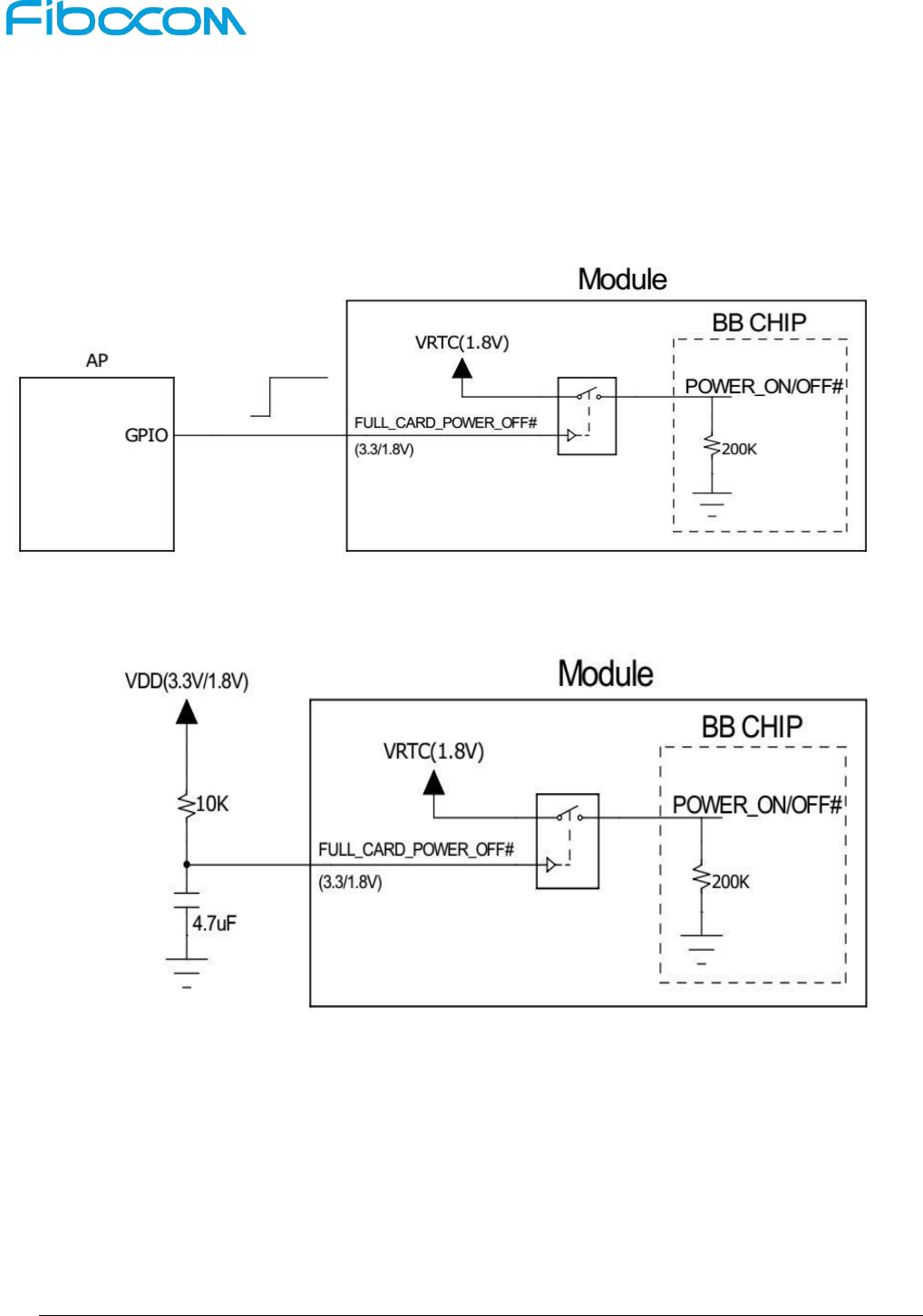
VDD(3.3V/1.8V) should be provided from the external circuit. Two methods for module starting up:
AP (Application Processor) controls the module start-up, and the circuit design is shown in Figure
3-4:
Automatically start-up when powered on, and the circuit design is shown in Figure 3-5:
Figure 3-4 Circuit for Module Start-up Controlled by AP
Figure 3-5 Circuit for Automatic Start-up
3.3.1.2 Start-up Timing Sequence
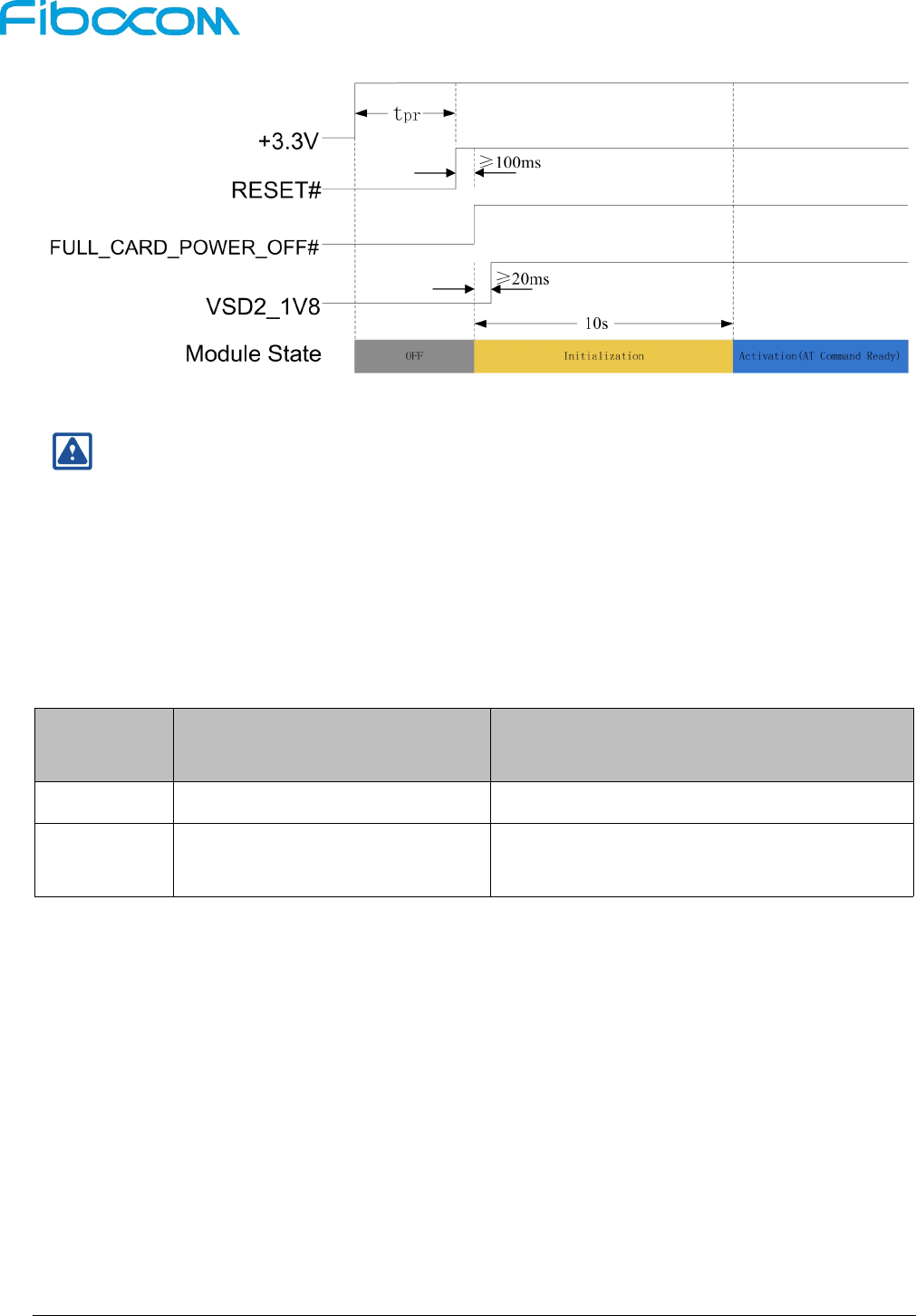
After powering on, the module will start-up by pulling up the FULL_CARD_POWER_OFF# signal for more
than 20ms (100ms is recommended). Meanwhile, the module will output 1.8V voltage through VSD2_1V8
pin and start the initialization process. The start-up timing is shown in Figure 3-6:
Reproduction forbidden without Fibocom Wireless Inc. written authorization - All Rights Reserved.
L830-EB Hardware User Manual Page 19 of 41
Figure 3-6 Timing Control for Start-up
Note:
The VSD2_1V8 signal is the internal PMU 1.8V output voltage which is not connected to the M.2
interface. The above timing of VSD2_1V8 is only for reference.
tpr:The time for 3.3V power rail becomes stable due to the capacitor charging.If + 3.3 V keeps
constant supply, the delay time can be ignored.
3.3.2 Module Shutdown
The module can be shutdown by the following controls:
Shutdown
Control
Action
Condition
Software
Sending AT+CFUN=0 command
Normal shutdown.
Hardware
Pull down
FULL_CARD_POWER_OFF# pin
Only used when a hardware exception occurs
and the software control cannot be used.
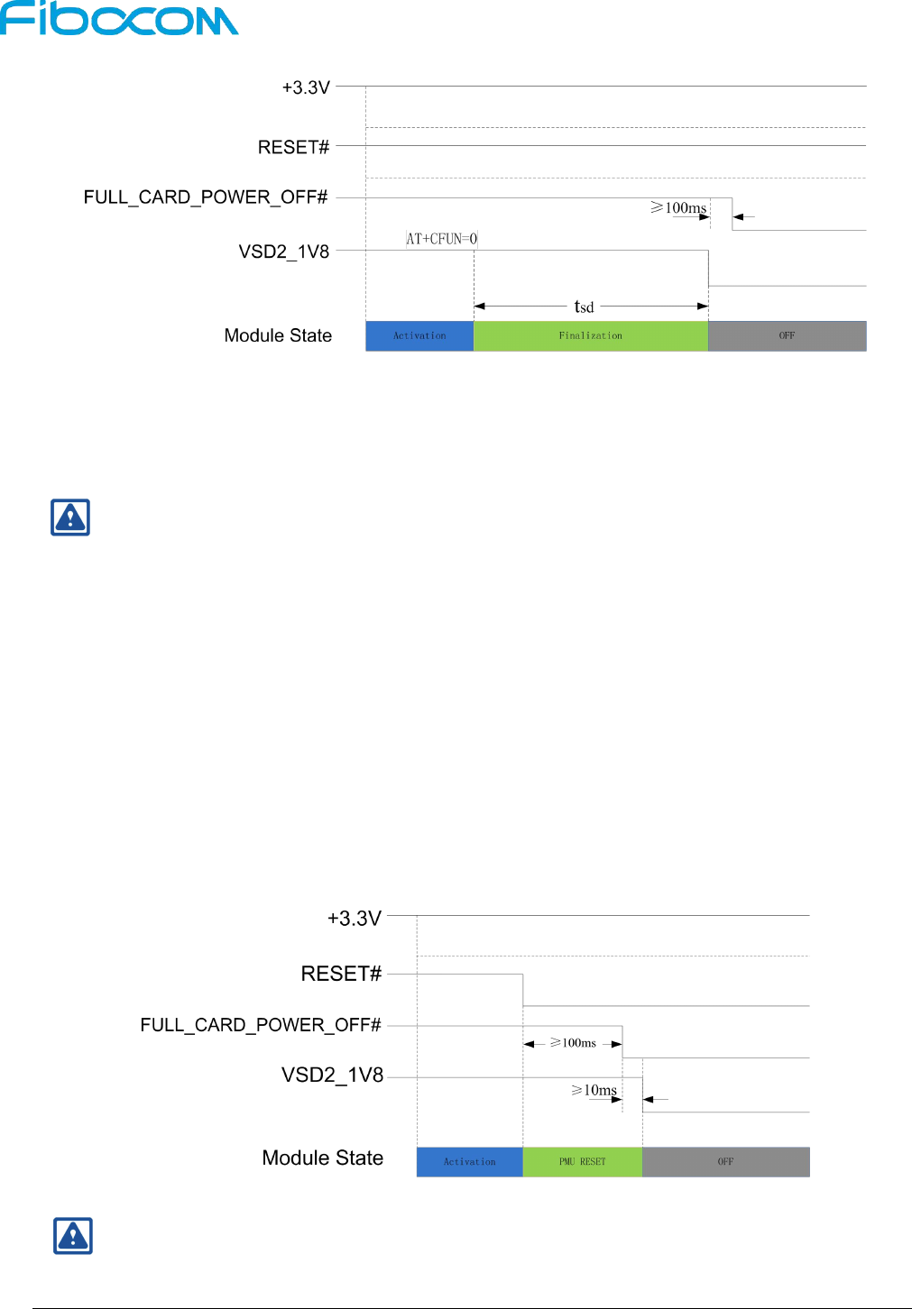
3.3.2.1 Software Shutdown
The module can be shut down by sending AT+CFUN=0 command. When the module receives the
software shutdown command, the module will start the finalization process (the reverse process of
initialization), and it will be completed after tsd time(tsd is the time which AP receive OK of “AT+CFUN=0”,if
there is no response, the max tsd is 5s). In the finalization process, the module will save the network, SIM
card and some other parameters from memory, then clear the memory and PMU will be powered off. After
shutdown, the VSD2_1V8 voltage is also shut down. The software control timing is shown in Figure 3-7:
Reproduction forbidden without Fibocom Wireless Inc. written authorization - All Rights Reserved.
L830-EB Hardware User Manual Page 20 of 41
Figure 3-7 Software Shutdown Timing Control
After the software shutdown, the FULL_CARD_POWER_OFF # pin will remain high which prevents the
module from restarting again. To enable the next restart, the FULL_CARD_POWER_OFF# pin should be
pulled low after shutting down.
Note:
The VSD2_1V8 signal is the internal PMU 1.8V output voltage which is not connected to the M.2
interface. The above timing of VSD2_1V8 is only for reference.
3.3.2.2 Hardware Shutdown
By pulling down the FULL_CARD_POWER_OFF# pin for more than 50ms (100ms is recommended), the
power management unit (PMU) of the module loses its power, and then the module will shut down by the
hardware. Because the PMU will lose its power by pulling down the FULL_CARD_POWER_OFF# pin, to
avoid damaging the module with power on/off procedures, it’s necessary to pull down RESET_N pin for
≧100ms before pulling down the FULL_CARD_POWER_OFF# pin. The hardware control timing is
shown in Figure 3-8:
Figure 3-8 Hardware Shutdown Timing Control
Note:
The VSD2_1V8 signal is the internal PMU 1.8V output voltage which is not connected to the M.2
Reproduction forbidden without Fibocom Wireless Inc. written authorization - All Rights Reserved.
L830-EB Hardware User Manual Page 21 of 41
interface. The above timing of VSD2_1V8 is only for reference.
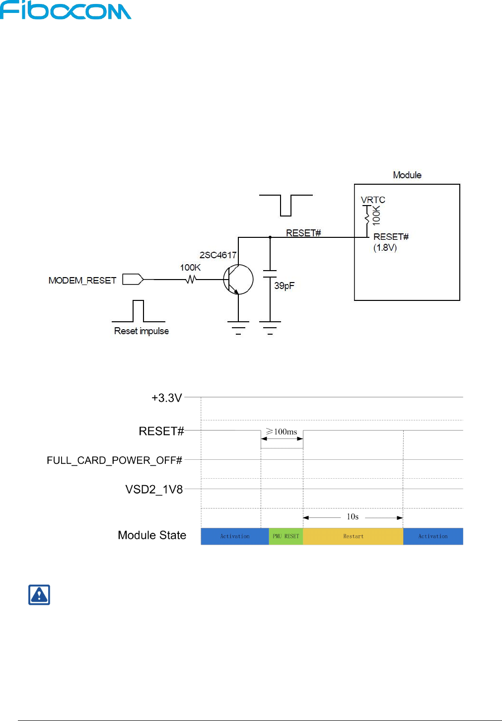
3.3.3 Module Reset
The L830 module can reset to its initial status by pulling down the RESET# signal for ≥100ms, and the
module will restart after the RESET# signal is released. When the customer executes RESET# function,
the PMU remains its power inside the module. The recommended circuit design is shown in the Figure
3-9:
Figure 3-9 Recommended Design for Reset Circuit
The reset control timing is shown in Figure 3-10:
Figure 3-10 Reset Timing Control
Note:
RESET# is a sensitive signal, it’s recommended to add a filter capacitor close to the module. In
case of PCB layout, the RESET# signal lines should keep away from the RF interference and
protected by GND. Also, the RESET# signal lines shall neither near the PCB edge nor route on
the surface planes to avoid module from reset caused by ESD problems.
Reproduction forbidden without Fibocom Wireless Inc. written authorization - All Rights Reserved.
L830-EB Hardware User Manual Page 22 of 41
3.4 USB Interface
The L830 module supports USB 2.0 which is compatible with USB High-Speed (480 Mbit/s) and USB
Full-Speed (12 Mbit/s). For the USB timing and electrical specification of L830 module, please refer to
“Universal Serial Bus Specification 2.0” .
For L830 module, the USB driver will export 1 MBIM and 1 GNSS device on Win10 system(It will map 3
ACM and 3 NCM ports for Android/Linux). For system switch function, please refer to chapter 3.7.2.
The MBIM port is used to initiate data service;
As for the 3 ACM ports, 2 COM ports are used for sending AT commands, another COM port is
used for LOG capture by software. The 3 NCM ports are used as virtual network ports to initiate
data service.
Note :
One COM port can be used as the Modem COM port to initiate the data service. Since the speed
of the Modem COM port is not sufficient for the 300 Mbps peak downlink speed requirement for
LTE, so it is not recommended to be used.
3.4.1 USB Interface Definition
Pin#
Pin Name
I/O
Reset Value
Description
Type
7
USB_D+
I/O
T
USB Data Plus
0.3---3V, USB2.0
9
USB_D-
I/O
T
USB Data Minus
0.3---3V, USB2.0
3.4.2 USB Interface Application
The reference circuit is shown in Figure 3-11:
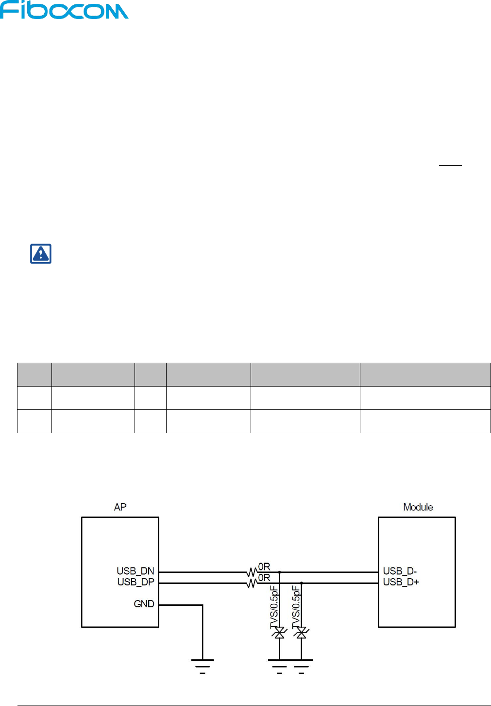
Figure 3-11 Reference Circuit for USB 2.0 Interface
Reproduction forbidden without Fibocom Wireless Inc. written authorization - All Rights Reserved.
L830-EB Hardware User Manual Page 23 of 41
Since the module supports USB 2.0 High-Speed, it is required to use TVS diodes with equivalent
capacitance of 1pF or smaller ones on the USB_D-/D+ differential signal lines, it is recommended to use
0.5pF TVS diodes.
USB_D- and USB_D+ are high speed differential signal lines with the maximum transfer rate of 480 Mbit/s,
so the following rules shall be followed carefully in the case of PCB layout:
USB_D- and USB_D+ signal lines should have the differential impedance of 90 ohms.
USB_D- and USB_D+ signal lines should be parallel and have the equal length, the right angle
routing should be avoided.
USB_D- and USB_D+ signal lines should be routed on the layer that is adjacent to the ground
layer, and wrapped with GND vertically and horizontally.
3.5 USIM Interface
The L830 module supports USIM card interface including 1.8V and 3V SIM cards.
3.5.1 USIM Pins
The USIM pins description as shown in the following table:
Pin
Pin Name
I/O
Reset Value
Description
Type
36
UIM_PWR
PO
USIM power supply
1.8V/3V
30
UIM_RESET
O
L
USIM reset
1.8V/3V
32
UIM_CLK
O
L
USIM clock
1.8V/3V
34
UIM_DATA
I/O
L
USIM data, internal 4.7K pull-up
1.8V/3V
66
SIM_DETECT
I
USIM card detect, internal 390K
pull-up.
Active high, and high level indicates
SIM card is inserted; and low level
indicates SIM card is detached.
1.8V
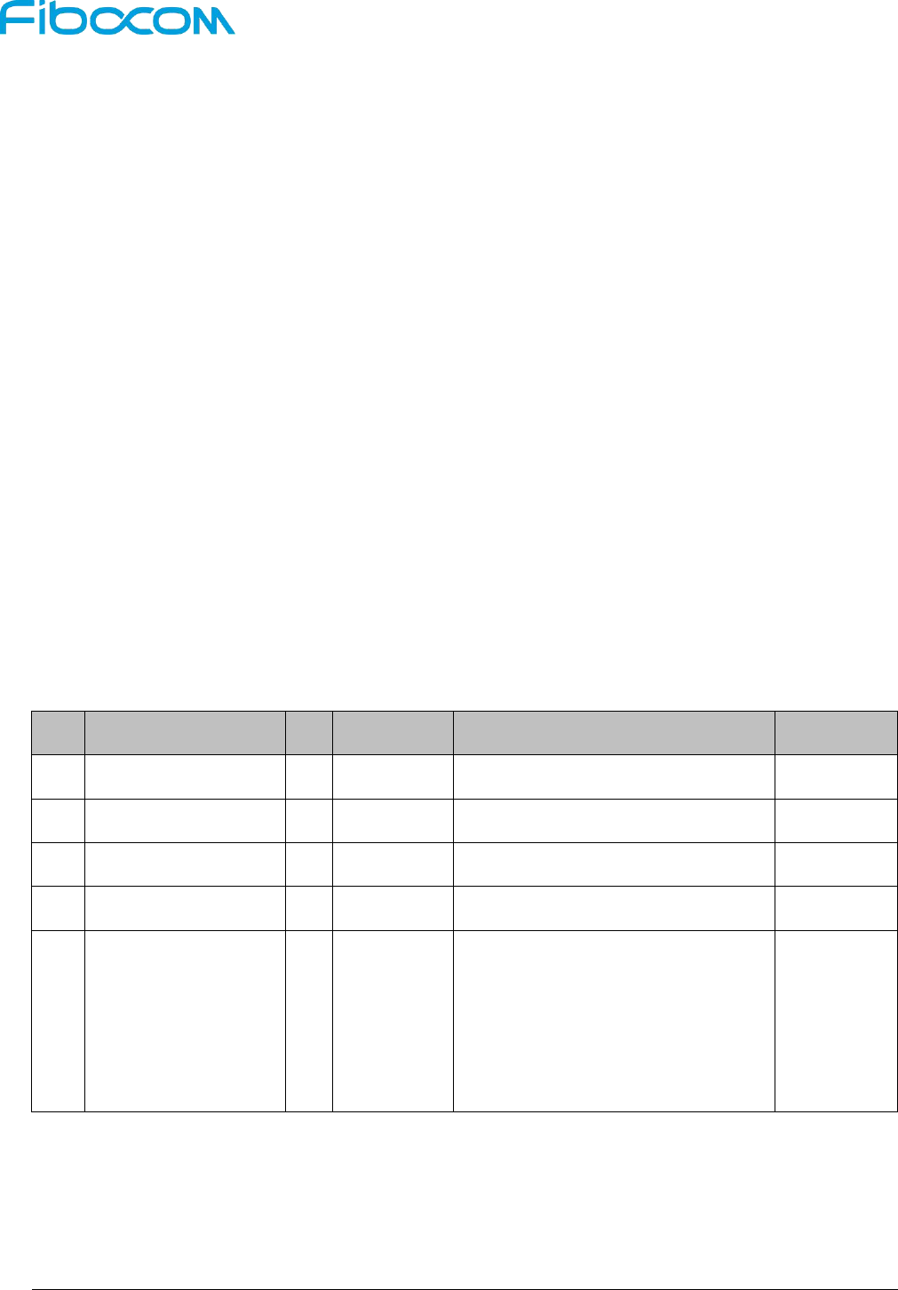
3.5.2 USIM Interface Circuit
3.5.2.1 N.C. SIM Card Slot
The reference circuit design for N.C. (Normally Closed) SIM card slot is shown in Figure 3-12:
Reproduction forbidden without Fibocom Wireless Inc. written authorization - All Rights Reserved.
L830-EB Hardware User Manual Page 24 of 41
Figure 3-12 Reference Circuit for N.C. SIM Card Slot
The principles of the N.C. SIM card slot are described as follows:
When the SIM card is detached, it connects the short circuit between CD and SW pins, and drives the
SIM_DETECT pin low.
When the SIM card is inserted, it connects an open circuit between CD and SW pins, and drives the
SIM_DETECT pin high.
3.5.2.2 N.O. SIM Card Slot
The reference circuit design for N.O. (Normally Open) SIM card slot is shown in Figure 3-13:
Figure 3-13 Reference Circuit for N.O. SIM Card Slot
The principles of the N.O. SIM card slot are described as follows:
When the SIM card is detached, it connects an open circuit between CD and SW pins, and
drives the SIM_DETECT pin low.

Reproduction forbidden without Fibocom Wireless Inc. written authorization - All Rights Reserved.
L830-EB Hardware User Manual Page 25 of 41
When the SIM card is inserted, it connects the short circuit between CD and SW pins, and drives
the SIM_DETECT pin high.
3.5.3 USIM Hot-Plugging
The L830 module supports the SIM card hot-plugging function, which determines whether the SIM card is
inserted or detached by detecting the SIM_DETECT pin state of the SIM card slot.
The SIM card hot-plugging function can be configured by “AT+MSMPD” command, and the description for
AT command as shown in the following table:
AT Command
Hot-plugging Detection
Function Description
AT+MSMPD=1
Enable
Default value, the SIM card hot-plugging detection function
is enabled.
The module can detect whether the SIM card is inserted or
not through the SIM_DETECT pin state.
AT+MSMPD=0
Disable
The SIM card hot-plugging detect function is disabled.
The module reads the SIM card when starting up, and the
SIM_DETECT status will not be detected.
After the SIM card hot-plugging detection function is enabled, the module detects that the SIM card is
inserted when the SIM_DETECT pin is high, then executes the initialization program and finish the
network registration after reading the SIM card information. When the SIM_DETECT pin is low, the
module determines that the SIM card is detached and does not read the SIM card.
Note:
By default, SIM_DETECT is active-high, which can be switched to active-low by the AT
command. Please refer to the AT Commands Manual for the AT command.
The system doesn’t need SIM hot-plug function, please left SIM_DTECT floating.
3.5.4 USIM Design
The SIM card circuit design shall meet the EMC standards and ESD requirements with the improved
capability to resist interference, to ensure that the SIM card can work stably. The following guidelines
should be noted in case of design:

Reproduction forbidden without Fibocom Wireless Inc. written authorization - All Rights Reserved.
L830-EB Hardware User Manual Page 26 of 41
The SIM card slot placement should near the module as close as possible, and away from the
RF antenna, DC/DC power supply, clock signal lines, and other strong interference sources.
The SIM card slot with a metal shielding housing can improve the anti-interference ability.
The trace length between the SIM card slot and the module should not exceed 100mm, or it
could reduce the signal quality.
The UIM_CLK and UIM_DATA signal lines should be isolated by GND to avoid crosstalk
interference. If it is difficult for the layout, the whole SIM signal lines should be wrapped with
GND as a group at least.
The filter capacitors and ESD devices for SIM card signals should be placed near to the SIM
card slot, and the ESD devices with 22~33pF capacitance should be used.
3.6 Status Indicator
The L830 module provides three signals to indicate the operating status of the module, and the status
indicator pins as shown in the following table:
Pin
Pin Name
I/O
Reset Value
Pin Description
Type
10
LED1#
O
PD
System status LED, drain
output.
CMOS 3.3V
23
WOWWAN#
O
PU
Module wakes up Host (AP).
CMOS 1.8V
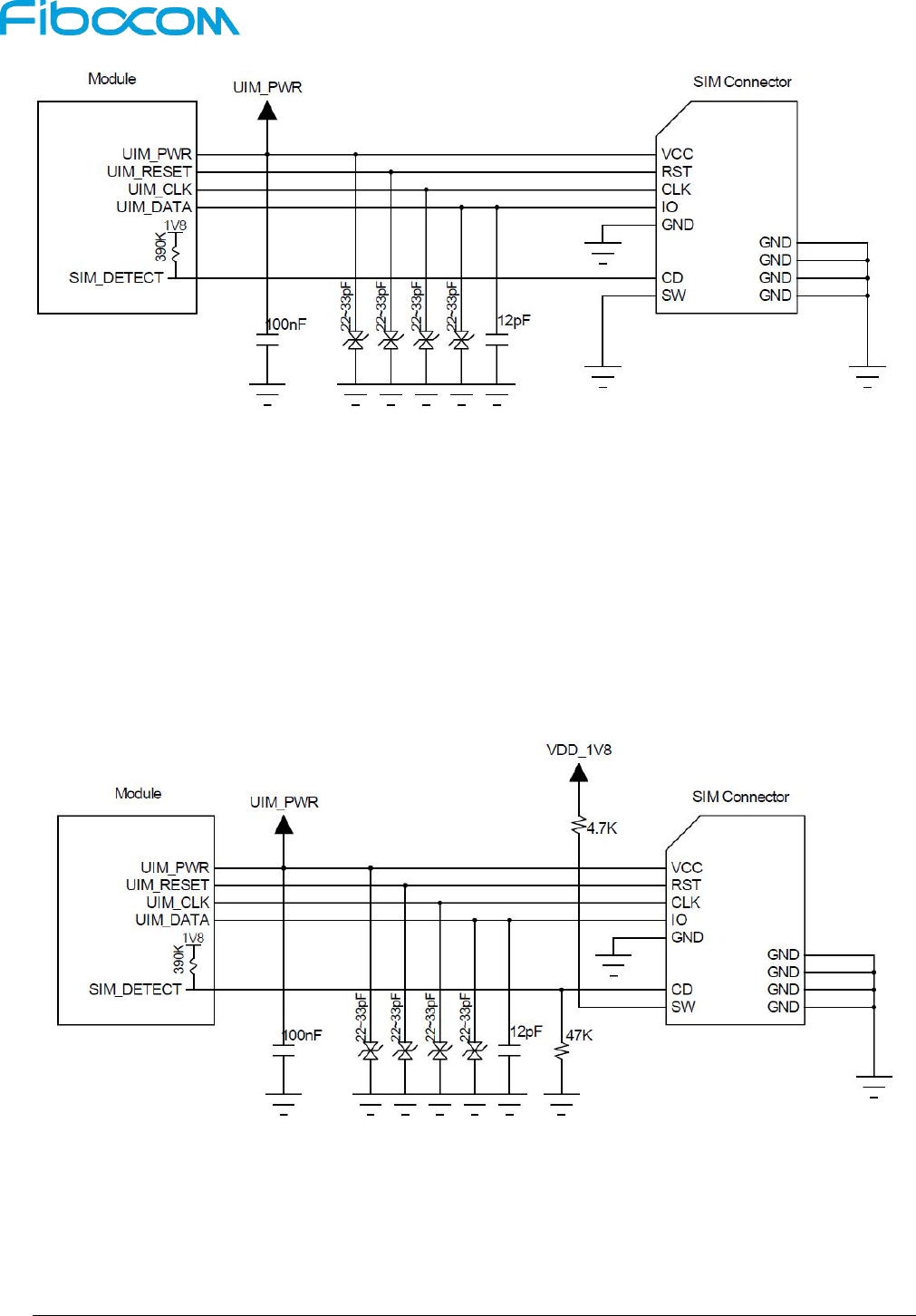
3.6.1 LED#1 Signal
The LED#1 signal is used to indicate the operating status of the module, and the detailed description as
shown in the following table:
Module Status
LED1# Signal
RF function ON
Low level (LED On)
RF function OFF
High level (LED Off)
The LED driving circuit is as follows:
Reproduction forbidden without Fibocom Wireless Inc. written authorization - All Rights Reserved.
L830-EB Hardware User Manual Page 27 of 41
Figure 3-14 LED Driving Circuit
Note:
The resistance of LED current-limiting resistor is selected according to the driving voltage and
the driving current.
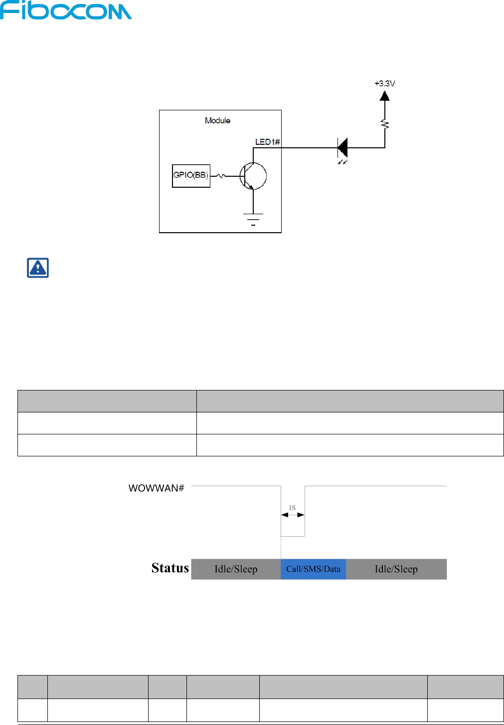
3.6.2 WOWWAN#
The WOWWAN# signal is used to wake the Host (AP) when there comes the data request. The definition
of WOWWAN# signal is as follows:
Operating Mode
WOWWAN# Signal
Ringing /SMS or data requests
Pull low 1s then pull high (pulse signal).
Idle/Sleep
High level
The WOWWAN# timing is shown in Figure 3-15:
Figure 3-15 WOWWAN# Timing
3.7 Interrupt Control
The L830 module provides four interrupt signals, and the pin definition is as follows:
Pin
Pin Name
I/O
Reset Value
Pin Description
Type
8
W_DISABLE1#
I
PU
Enable/Disable RF network
CMOS 3.3V
Reproduction forbidden without Fibocom Wireless Inc. written authorization - All Rights Reserved.
L830-EB Hardware User Manual Page 28 of 41
25
DPR
I
PU
Body SAR detection
CMOS 1.8V
26
W_DISABLE2#
I
PU
GNSS Disable signal (not
supported yet)
CMOS 1.8V
44
GNSS_IRQ
I
PU
MBIM/ACM system port switch
CMOS 1.8V
3.7.1 W_DISABLE1#
The module provides a hardware pin to enable/disable WWAN RF function, and the function can also be
controlled by the AT command. The module enters the Flight mode after the RF function is disabled. The
definition of W_DISABLE1# signal is as follows:
W_DISABLE1# signal
Function
High/Floating
WWAN function is enabled, the module exits the Flight mode.
Low
WWAN function is disabled, the module enters Flight mode.
3.7.2 System Switch Control
The module can be switched between ACM and MBIM interfaces for Android/Linux/Win7 and
Win8.1/Win10 systems respectively. The system switch function can be achieved by detecting the
GNSS_IRQ interrupt signal. The definition for GNSS_IRQ signal function is as follows:
GNSS_IRQ signal
Function
High/Floating
The USB interface mapped as a MBIM port, which supports Win8.1 / Win10
system.
Low
The USB interface mapped as the ACM ports, which supports Android / Linux /
Win7 system.
Description:
During booting, it will switch to ACM or MBIM interfaces by detecting the level of GNSS_IRQ signal.
The voltage level of GNSS_IRQ should be kept stable during booting.
After booting, it will switch to ACM or MBIM interfaces by detecting the rising or falling edge of the
GNSS_IRQ interrupt with the filtering time of 100ms. If the interrupt event meets the condition, the
module will restart and change over its USB mode for the desired interface.
3.7.3 Body SAR
The L830 module supports Body SAR function by detecting the DPR pin. The voltage level of DPR is high
by default, and when the SAR sensor detects the closing human body, the DPR signal will be pulled down.
As the result, the module then lowers down its emission power to its default threshold value, thus
Reproduction forbidden without Fibocom Wireless Inc. written authorization - All Rights Reserved.
L830-EB Hardware User Manual Page 29 of 41
reducing the RF radiation on the human body. The threshold of emission power can be set by the AT
Commands. The definition of DPR signal as shown in the following table:
DPR signal
Function
High/Floating
The module keeps the default emission power
Low
Lower the maximum emission power to the threshold value of the module.
3.8 Digital Audio
The L830 module supports I2S digital audio interface and it supports the ordinary I2S mode and PCM
mode. The signal level of the I2S interface is 1.8V. Please refer to “FIBOCOM Digital Voice” description
for detailed application design. The definition of I2S signals is as follows:
Pin
Pin Name
I/O
Reset Value
Pin Description
Type
20
I2S_CLK
O
PD
I2S clock
CMOS 1.8V
22
I2S_RX
I
PD
I2S serial data receive
CMOS 1.8V
24
I2S_TX
O
PD
I2S serial data transmit
CMOS 1.8V
26
I2S_WA
O
PD
I2S left and right channel clock (LRCK)
CMOS 1.8V
.
3.8.1 I2S Mode
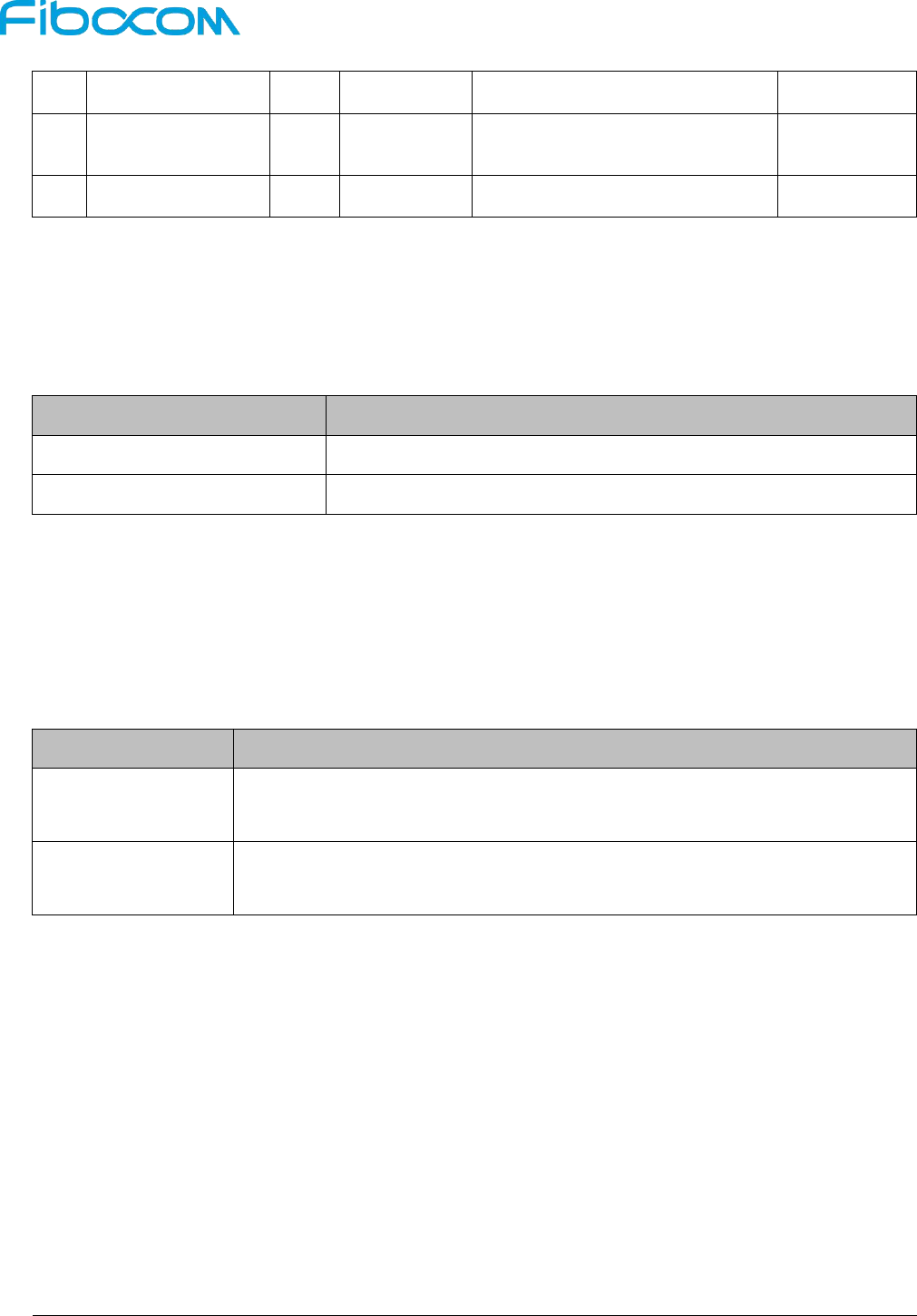
The L830 module is connected to the Audio Codec via I2S interface, and the codec encodes the audio
data to implement the voice call function. For the scenario, the module works as the I2S master, and the
codec works as the I2S slave. I2S signal connection is shown in Figure 3-18:
Figure 3-18 I2S Signal Connection
Description:
I2S interface can be configured as master or slave mode.
It supports multiple audio sampling rates (44.1KHz,32KHz,24KHz,16KHz,8KHz).
It supports 16bit and 32bit mode.
Reproduction forbidden without Fibocom Wireless Inc. written authorization - All Rights Reserved.
L830-EB Hardware User Manual Page 30 of 41
3.8.2 PCM Mode
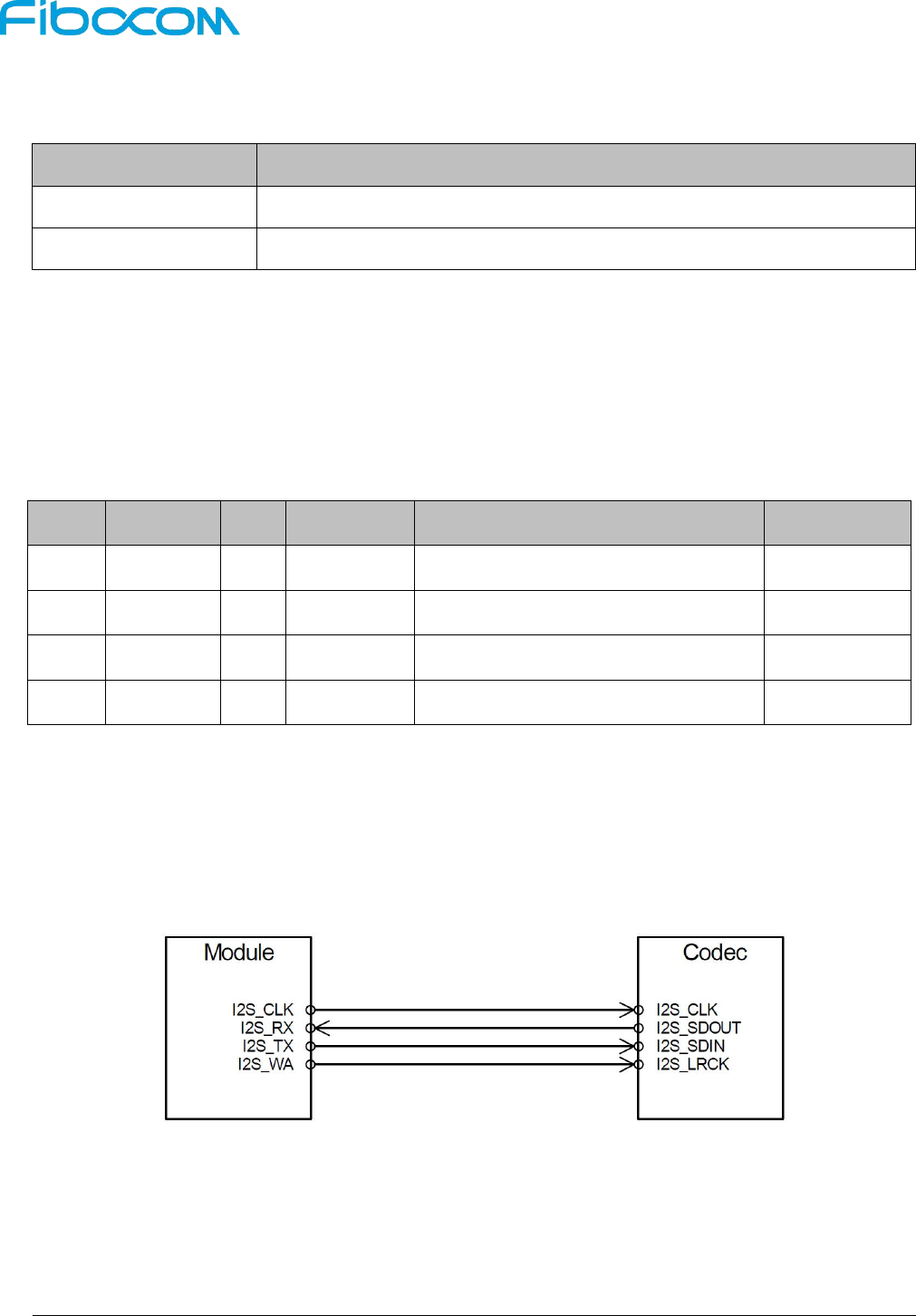
In the case of the Bluetooth (BT) call, the PCM mode is used to transmit digital voice data if the BT chip
does not support I2S. For the scenario, the module works as the PCM master, and BT works as the PCM
slave mode. The signal connection under the PCM mode is shown in Figure 3-19:
Figure 3-19 Signal Connection for PCM Mode
Description:
The PCM mode interface can be configured as master or slave mode.
It supports various audio sampling rates (444.1KHz,32KHz,24KHz,16KHz,8KHz).
It supports short frame sync for 16 and 32 bit mode.
It supports burst and continuous transmission modes.
It supports clock length trigger for frame sync signal and rising/falling edge trigger for data
transmission.
Note:
The PCM mode timing is relative complicated to adjust, and the audio quality will be reduced if it
is not fine tuned. In contrast to PCM mode, I2S mode is easier to adjust, hence it is
recommended to use I2S mode.
3.9 I2C Interface Description
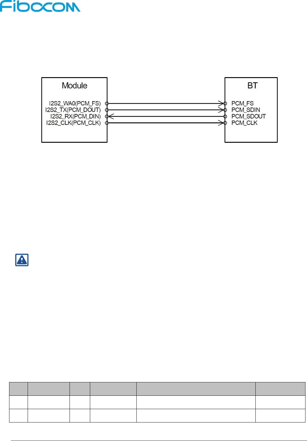
The L830 module supports one I2C interface, which is configured as I2C master by default. The I2C
master is used for driving external I2C slave devices, such as the Audio Codec.
Pin
Pin Name
I/O
Reset Value
Pin Description
Type
40
GNSS_SCL
O
PU
I2C serial data, internal 4.7KΩ pull up.
CMOS 1.8V
42
GNSS_SDA
I/O
PU
I2C serial clock, internal 4.7KΩ pull up.
CMOS 1.8V
Reproduction forbidden without Fibocom Wireless Inc. written authorization - All Rights Reserved.
L830-EB Hardware User Manual Page 31 of 41
The module is connected to the external I2C slave devices (e.g. Audio Codec), which is as follows:
Figure 3-20 I2C Signal Connection
Note:
The I2C interface pins can be left floating if not used.
3.10 Clock Interface
The L830 module supports a clock interface, it can output 26MHz clock.
Pin
Pin Name
I/O
Reset Value
Pin Description
Type
46
SYSCLK
O
26MHz clock output, can be used for
external GPS or Audio Codec.
1.8V
3.11 Configuration Interface
The L830 module provides four config pins for the configuration as the WWAN-SSIC-0 type M.2 module:
Pin
Pin Name
I/O
Reset Value
Pin Description
Type
1
CONFIG_3
O
L
Internally connected to GND
21
CONFIG_0
O
NC
69
CONFIG_1
O
L
Internally connected to GND
75
CONFIG_2
O
L
Internally connected to GND
The M.2 module configuration as the following table:
Config_0
(pin21)
Config_1
(pin69)
Config_2
(pin75)
Config_3
(pin1)
Module Type and Main
Host Interface
Port
Configuration
NC
GND
GND
GND
WWAN-SSIC
0
Please refer to “PCI_Express_M.2_Specification_Rev1.1” for more details.
Reproduction forbidden without Fibocom Wireless Inc. written authorization - All Rights Reserved.
L830-EB Hardware User Manual Page 32 of 41
3.12 Other Interfaces
The module does not support ANT Tunable interface yet.
4 Radio Frequency
4.1 RF Interface
4.1.1 RF Interface Functionality
The L830 module supports two RF connectors used for external antenna connection. As the
Figure 4-1 shows, “M” is for Main antenna, used to receive and transmit RF signals; “D/G” is
for Diversity and GNSS antenna, used to receive the diversity and GNSS RF signals.
Figure 4-1 RF connectors
4.1.2 RF Connector Characteristic
Rated Condition
Environment Condition
Frequency Range
DC to 6GHz
Temperature Range
Characteristic Impedance
50Ω
–40°C to +85°C
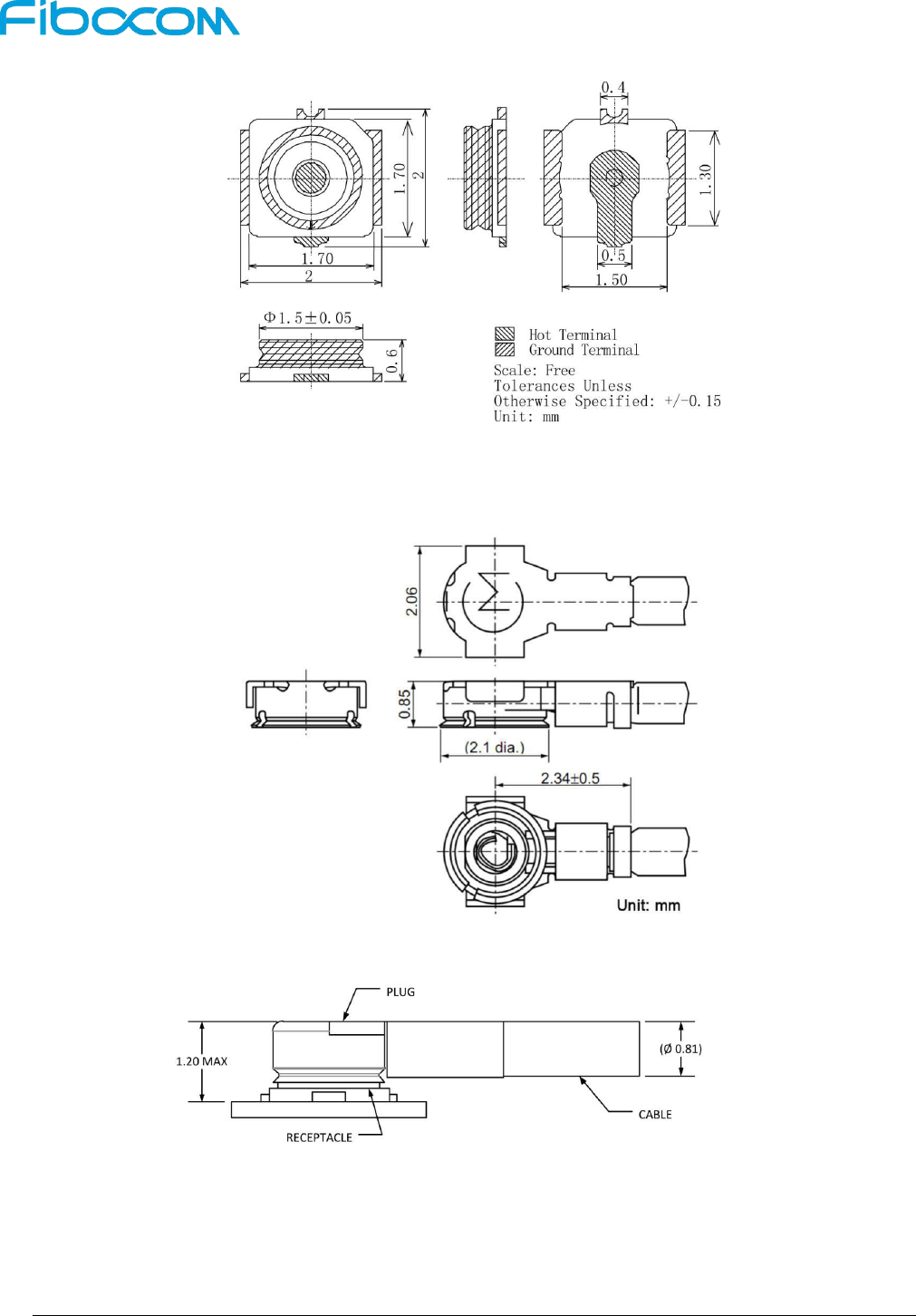
4.1.3 RF Connector Dimension
The L830 module adopts standard M.2 module RF connectors, the model name is 818004607 from ETC
company, and the connector size is 2*2*0.6m. The connector dimension is shown as following picture:
Reproduction forbidden without Fibocom Wireless Inc. written authorization - All Rights Reserved.
L830-EB Hardware User Manual Page 33 of 41
Figure 4-2 RF connector dimensions
Figure 4-3 0.81mm coaxial antenna dimensions
Figure 4-4 Schematic diagram of 0.81mm coaxial antenna connected to the RF connector
Reproduction forbidden without Fibocom Wireless Inc. written authorization - All Rights Reserved.
L830-EB Hardware User Manual Page 34 of 41
4.2 Operating Band
The L830 module operating bands of the antennas are as follows:
Operating
Band
Description
Mode
Tx (MHz)
Rx (MHz)
Band 1
IMT 2100MHz
LTE FDD/WCDMA
1920 - 1980
2110 - 2170
Band 3
DCS 1800MHz
LTE FDD
1710 - 1785
1805 - 1880
Band 5
CLR 850MHz
LTE FDD/WCDMA
824 - 849
869 - 894
Band 7
IMT-E 2600Mhz
LTE FDD
2500 - 2570
2620 - 2690
Band 8
E-GSM 900MHz
LTE FDD/WCDMA
880 - 915
925 - 960
Band 20
EUDD 800MHz
LTE FDD
832 - 862
791 - 821
Band 28
APT700
LTE FDD
703-748
758-803
GPS L1
N/A
1575.42±1.023
GLONASS L1
N/A
1602.5625±4
4.3 Transmitting Power
The transmitting power for each band of the L830 module as shown in the following table:
Mode
Band
3GPP Requirement
Tx Power(dBm)
Note
WCDMA
Band I
24+1.7/-3.7
23.5±1
Band V
24+1.7/-3.7
23.5±1
Band VIII
24+1.7/-3.7
23.5±1
LTE FDD
Band 1
23±2.7
23±1
10MHz Bandwidth, 1 RB
Band 3
23±2.7
23±1
10MHz Bandwidth, 1 RB
Band 5
23±2.7
23±1
10MHz Bandwidth, 1 RB
Band 7
23±2.7
23±1
10MHz Bandwidth, 1 RB
Band 8
23±2.7
23±1
10MHz Bandwidth, 1 RB
Band 20
23±2.7
23±1
10MHz Bandwidth, 1 RB
Band 28
23+2.7/-3.2
23±1
10MHz Bandwidth, 1 RB
Reproduction forbidden without Fibocom Wireless Inc. written authorization - All Rights Reserved.
L830-EB Hardware User Manual Page 35 of 41
4.4 Receiver Sensitivity
The receiver sensitivity for each band of the L830 module as shown in the following table:
Mode
Band
3GPP Requirement
Rx Sensitivity(dBm)
Typical
Note
WCDMA
Band I
-106.7
-110
BER<0.1%
Band V
-104.7
-110
BER<0.1%
Band VIII
-103.7
-110.5
BER<0.1%
LTE FDD
Band 1
-96.3
-101
10MHz Bandwidth
Band 3
-93.3
-101
10MHz Bandwidth
Band 5
-94.3
-101.5
10MHz Bandwidth
Band 7
-94.3
-101.5
10MHz Bandwidth
Band 8
-93.3
-101
10MHz Bandwidth
Band 20
-93.3
-101
10MHz Bandwidth
Band 28
-94.8
-101
10MHz Bandwidth
Note:
The above values are measured for the dual antennas situation (Main + Diversity). For single
main antenna (without Diversity), the sensitivity will drop around 3dBm for each band of LTE.
4.5 GNSS
L830 module support GPS, GLONASS and A-GPS. It uses RF Diversity & GNSS 2in1 antenna.
Description
Condition
Test Result
Power
GPS fixing
98.3mA /-130dBm
GPS tracking
99.9mA / -130dBm
GLONASS fixing
74.5mA / -130dBm
GLONASS tracking
75mA / -130dBm
GPS Sleep
3.5mA
GLONASS Sleep
3.5mA
TTFF
GPS
Cold start
34s / -130dBm
Warm start
32s / -130dBm
Hot Start
1s / -130dBm
Reproduction forbidden without Fibocom Wireless Inc. written authorization - All Rights Reserved.
L830-EB Hardware User Manual Page 36 of 41
Description
Condition
Test Result
GLONASS
Cold start
30s / -130dBm
Warm start
37s / -130dBm
Hot Start
1s / -130dBm
A-GPS
Cold start
TBD
Sensitivity
GPS
Acquisition
-146dBm
Tracking
-160dBm
GLONASS
Acquisition
-143dBm
Tracking
-158dBm
Note:
Please note GNSS consumption was tested in RF disable mode.
4.6 Antenna Design
The L830 module provides main and diversity antenna interfaces, and the antenna design requirements
as shown in the following table:
L830 module Main antenna requirements
Frequency range
The most proper antenna to adapt the frequencies should be used.
Bandwidth(WCDMA)
WCDMA band I(2100) : 250 MHz
WCDMA band V(850) : 70 MHz
WCDMA band VIII(900) : 80 MHz
Bandwidth(LTE)
LTE band 1(2100): 250 MHz
LTE Band 3(1800): 170 MHz
LTE band 5(850): 70 MHz
LTE band 7(2600): 190 MHz
LTE Band 8(900): 80 MHz
LTE band 20(800): 71 MHz
LTE band 28(850): 100 MHz
Bandwidth(GNSS)
GPS: 2MHz
GLONASS: 8MHz
Impedance
50 Ohm
Input power
> 25dBm average power WCDMA & LTE
Recommended
standing-wave ratio (SWR)
≤ 2:1
Reproduction forbidden without Fibocom Wireless Inc. written authorization - All Rights Reserved.
L830-EB Hardware User Manual Page 37 of 41
5 Structure Specification
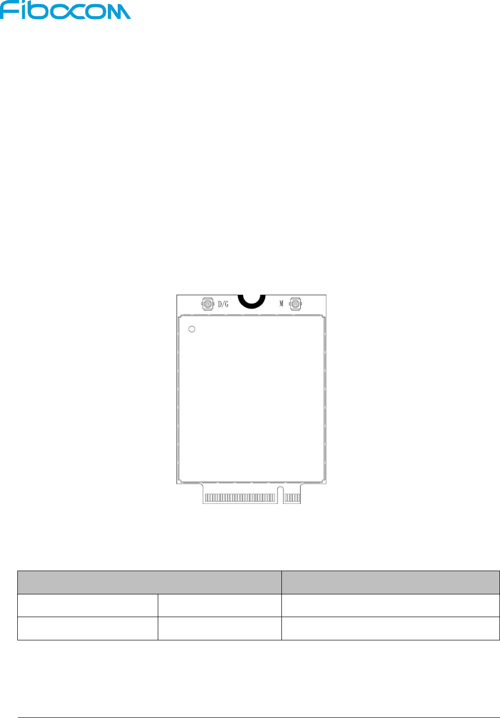
5.1 Product Appearance
The product appearance for L830 module is shown in Figure 5-1:
Figure 5-1 Module Appearance
5.2 Dimension of Structure
The structural dimension of the L830 module is shown in Figure 5-2:
Reproduction forbidden without Fibocom Wireless Inc. written authorization - All Rights Reserved.
L830-EB Hardware User Manual Page 38 of 41
Figure 5-2 Dimension of Structure
5.3 M.2 Interface Model
The L830 M.2 module adopts 75-pin gold finger as external interface, where 67 pins are signal pins and 8
pins are notch pins as shown in Figure 3-1. For module dimension, please refer to chapter 5.2. Based on
the M.2 interface definition, L830 module adopts Type 3042-S3-B interface (30x42mm, the component
maximum height on t top layer is 1.5mm, PCB thickness is 0.8mm, and KEY ID is B).
5.4 M.2 Connector
The L830 module connects to AP via M.2 connector, it is recommended to use M.2 connector from
LOTES company with the model APCI0026-P001A as shown in Figure 5-3. The package of connector,
please refer to the specification.
Reproduction forbidden without Fibocom Wireless Inc. written authorization - All Rights Reserved.
L830-EB Hardware User Manual Page 39 of 41
Figure 5-3 M.2 Dimension of Structure
5.5 Storage
5.5.1 Storage Life
Storage Conditions (recommended): Temperature is 23 ± 5 ℃, relative humidity is RH 35-70%.
Storage period (sealed vacuum packing): Under the recommended storage conditions, the storage life is
12 months.
5.6 Packing
The L830 module uses the tray sealed vacuum packing, combined with the outer packing method using
the hard cartoon box, so that the storage, transportation and the usage of modules can be protected to
the greatest extent.
Note:
The vacuum package bag includes the humidity card and a desiccant. The module is the
humidity sensitive device, and the humidity sensitivity level is Class 3, which meets the
requirements of the American Electronic Component Industry Association (JEDEC). Please read
the relevant application guidance and precautions referred to herein, to avoid the permanent
damage to the product caused by humidity.
Reproduction forbidden without Fibocom Wireless Inc. written authorization - All Rights Reserved.
L830-EB Hardware User Manual Page 40 of 41
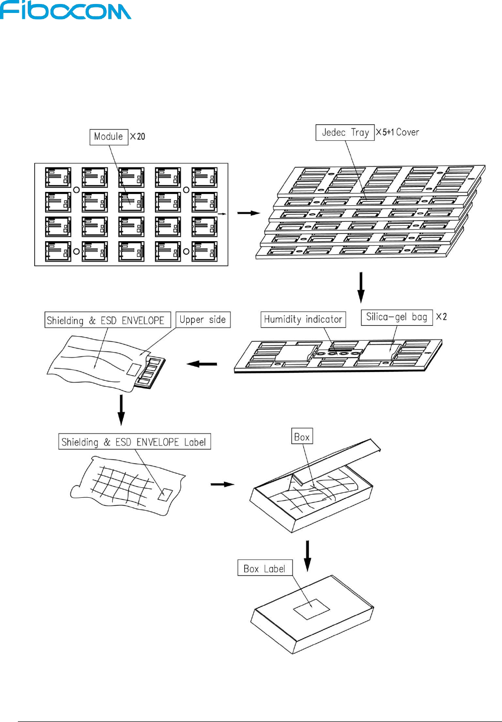
5.6.1 Tray Package
The L830 module uses tray package, 20 pcs are packed in each tray, with 5 trays in each box and 6
boxes in each case. Tray packaging process is shown in Figure 5-4:
Figure 5-4 Tray Packaging Process
Reproduction forbidden without Fibocom Wireless Inc. written authorization - All Rights Reserved.
L830-EB Hardware User Manual Page 41 of 41
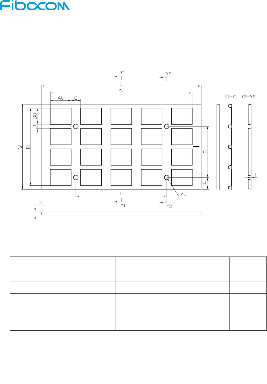
5.6.2 Tray size
The pallet size is 330*175*6.0mm, as shown in Figure 5-5:
ITEM L W H T A0 B0
DIM 330.0±0.5 175.0±0.5 6.0±0.3 0.5±0.1 43±0.3 33.0±0.3
ITEM A1 B1 C D E F
DIM 294.0±0.3 159.0±0.3 20.0±0.5 9.0±0.5 24.5±0.5 187.5±0.2
ITEM G J
DIM 105.0±0.2 9.0±0.2
Figure 5-5 Tray Size (Unit: mm)