Fisher Price DPV70-01 Bluetooth Module User Manual
Fisher-Price Inc. Bluetooth Module
User Manual
WMD410A01MT6A0 (HY-254101M) Use TTC2541 /TI CC2541 IC chip
24 pin BLE Bluetooth module (with shield case) specifications.
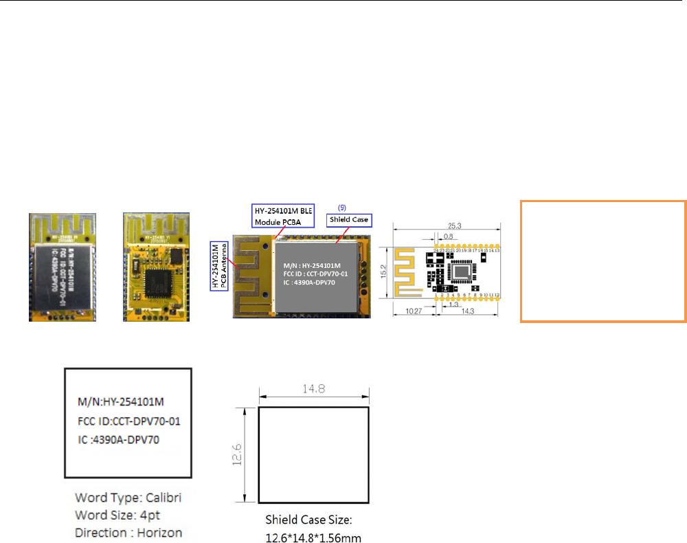
1. Dimensions
(1-1).DIMENSION SIZE :
(1-2): FCC ID & IC ID Laser Print Format on the Shield Case :
1 st row: M/N : HY-254101M
2 nd row: FCC ID : CCT-DPV70-01
3 rd row: IC : 4390A-DPV70
PCB SIZE:
15.2*25.3*1.0 mm
PCBA with shield
case Tickness:
2.6mm
2
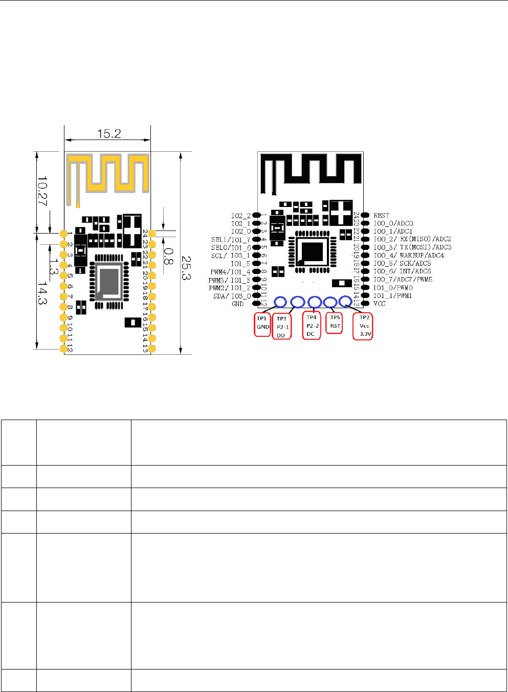
2. Module pin definition and description of input and output ports
(2-1)HY-254101C(WMD410A01MA6A0 PCB Antenna)pin map
(2-2)Pin function table (Not shown in the I/O pin functions ,Please see
Table (3-3) input and output ports description)
Pin
No. Function Function Description
1 IO2_2 / DC Digital I/O port 2_2 / Debug clock
2 IO2_1 / DD Digital I/O port 2_1 / Debug data
3 IO2_0 Digital I/O port 2_0
4 IO1_7 / SEL1
Digital I/O port 1_7
MCU communication mode select, See table(5-3)
Communication protcol mode selection, I/O setting Table
5 IO1_6 / SEL0
Digital I/O port 1_6
MCU communication mode select, See table(5-3)
Communication protcol mode selection, I/O setting Table
6 IO3_1 / Digital I/O port 3_1

3
I2C SCL
IIC serial Clock (SCL)
can be used as I2C clock pin or digital I/O. Leave floating
if not used. If grounded disable pull up
7 IO1_5 Digital I/O port 1_5
8 IO1_4 / PWM4 Digital I/O port 1_4 / PWM port 4
9 IO1_3 / PWM3 Digital I/O port 1_3 / PWM port 3
10 IO1_2 / PWM2 Digital I/O port 1_2 / PWM port 2
11 IO3_0 / I2C
SDA
Digital I/O port 3_0
I2C serial Data (SDA)
Can be used as I2C data pin or digital I/O. Leave floating
if not used. If grounded disable pull up
12 GND BLE module grounding pin
13 VCC BLE module power supply pin,
voltage range of 2.0 ~ 3.6V
14 IO1_1 / PWM1
Digital I/O port 1_1 20mA drive capability
/ PWM port 1
15 IO1_0 / PWM0
Digital I/O port 1_0 20mA drive capability
/ PWM port 0
16
IO0_7 Digital I/O port 0_7
ADC7 ADC port 7
PWM5 PWM port 5
17
IO0_6 Digital I/O port 0_6
INT Interrupt output pin
ADC 6 ADC port 6
18
IO0_5 Digital I/O port 0_5
SPI SCK SPI Bus clock signal
ADC 5 ADC port
19 IO0_4 Digital I/O port 0_4
WAKEUP BLE wake up pin, Low/ wake up, High / BLE module

4
automatically sleep
ADC4 ADC port 4
20
IO0_3 Digital I/O port 0_3
UART TX UART Serial data bus output
SPI MOSI SPI Master Out , Slave input
ADC3 ADC port 3
21
IO0_2 Digital I/O port 0_2
UART RX UART Serial data bus input
SPI MISO SPI Master input , Slave output
ADC2 ADC port 2
22 IO0_1 / ADC1 Digital I/O port 0_1 / ADC PORT 1
23 IO0_0 / ADC0 Digital I/O port 0_0 / ADC PORT 0
24 Reset BLE hardware reset pin (Low: reset)
Pin Function Description (The module following collectively "BLE"):
a. UART: serial bus, the default baud rate 9600bps, a single packet transmission
is less than 17 bytes, package transmission intervals greater than 20ms.
b. SPI: SPI bus interface, support for less than 2M / S data transmission rate,
a single packet transmission is less than 17 bytes, package
transmission intervals greater than 20ms.
c. IIC: IIC bus interface, support more than 22K / S, less than 400K / S data
transmission rate, a single packet transmission is less than 8 bytes,
package transmission intervals greater than 20ms.
d. MOSI: Master output, Slave input.
e. MISO: Master input, Slave output.
f. SCK: SPI bus clock signal.
g. SDA: IIC data.
h. SCL: IIC clock.
i. WAKEUP: BLE wake up pin, Low _wake up, High/ BLE module automatically sleep.
j. SEL0 & SEL1: MCU and BLE communication mode selection pin. Specific details,
see "(4-3) communication protocol mode selection, I/O setting table ".
k. RESET: BLE hardware reset pin, Low level reset.

5
l. VCC: BLE module power supply pin voltage range DC 2.0~3.6V.
m. GND: BLE module ground pin.
(2-3).Communication protocol mode selection, I/O setting Table
No.
Channel Select
PIN status
Communication
interface state
Remark
SEL1 SEL0 UART SPI IIC
1.Command mode
Please contact the
Vendor.
2.Description:
0 is Low,1 is high
1 0 0 OK X X
2 0 1 0K X X
3 1 0 X OK X
4 1 1 X X OK
5 X X OK X X
UART mode:SEL1=0,SEL0=0 or SEL1=0, SEL0=1 or SEL0,SEL1 floating.
SPI mode: SEL1=1,SEL0=0 IIC mode: SEL1=1,SEL0=1
Table(2-4): Input and output ports Description
Input / output Register pin No.
I/O Port
register
7 6 5 4 3 2 1 0
IO_0 16 17 18 19 20 21 22 23
IO_1 4 5 7 8 9 10 14 15
IO_2 NC NC NC NC NC 1 2 3
IO_3 NC NC NC NC NC NC 6 11
Note:BITx=0,Low level out ; BITx=1 High level out
6
Direction Register pin No.
Direction
Register
7 6 5 4 3 2 1 0
DIR0 16 17 18 19 20 21 22 23
DIR1 4 5 7 8 9 10 14 15
DIR2 NC NC NC NC NC 1 2 3
DIR3 NC NC NC NC NC NC 6 11
Note: BITx = 0 is corresponds port input , BITx = 1 is corresponds port output .
PWM port pin No.
PWM5 PWM4 PWM3 PWM2 PWM1 PWM0
16 8 9 10 14 15
ADC port pin No.
ADC7 ADC6 ADC5 ADC4 ADC3 ADC2 ADC1 ADC0
16 17 18 19 20 21 22 23
Note: The Blue Numbers of the corresponding port pin No. applications of all
kinds, For example:IO0/bit0 or ADC0 pin is corresponding module pin No.23
Note: This module cannot connect to the external antenna. It has to use the
existing antenna (PCB Antenna).

7
(3). FCC/Industry Canada Statement (to be placed on End Products)
Federal Communications Commission (FCC) Statement
This equipment has been tested and found to comply with the limits for a Class
B digital device, pursuant to part 15 of the FCC rules. These limits are designed
to provide reasonable protection against harmful interference in a residential
installation. This equipment generates, uses and can radiate radio frequency
energy and, if not installed and used in accordance with the instructions, may
cause harmful interference to radio communications.
However, there is no guarantee that interference will not occur in a
particular installation. If this equipment does cause harmful interference to
radio or television reception, which can be determined by turning the equipment
off and on, the user is encouraged to try to correct the interference by one
or more of the following measures:
‐Reorient or relocate the receiving antenna.
‐ Increase the separation between the equipment and receiver.
‐Connect the equipment into an outlet on a circuit different from that to
which the receiver is connected.
‐Consult the dealer or an experienced radio/TV technician for help.
This device complies with Part 15 of the FCC Rules. Operation is subject to
the following two conditions:
1) This device may not cause harmful interference, and
2) This device must accept any interference received, including
interference that may cause undesired operation of the device.

8
FCC RF Radiation Exposure Statement:
This equipment complies with FCC radiation exposure limits set forth for
an uncontrolled environment. End users must follow the specific operating
instructions for satisfying RF exposure compliance. This transmitter must not
be co‐located or operating in conjunction with any other antenna or
transmitter.
Industry Canada (IC) Statement
This device complies with Industry Canada’s licence-exempt RSSs.
Operation is subject to the following two conditions:
(1) This device may not cause interference; and
(2) This device must accept any interference, including interference that may
cause undesired operation of the device.
Canada, avis d’Industry Canada (IC)
Le présent appareil est conforme aux CNR d'Industrie Canada applicables
aux appareils radio exempts de licence. L'exploitation est autorisée aux deux
conditions suivantes:
(1) l'appareil ne doit pas produire de brouillage;
(2) l'utilisateur de l'appareil doit accepter tout brouillage
radioélectrique subi, même si le brouillage est susceptible d'en
compromettre le fonctionnement.
FCC CAUTION
Changes or modifications not expressly approved by the party responsible
for compliance could void the user’s authority to operate the equipment.

9
Notice to OEM integrator
The end user manual shall include all required regulatory information/warning
as show in this manual.
The OEM integrator is responsible for testing their end‐product for any
additional compliance requirements required with this module installed.
If the FCC ID is not visible when the module is installed inside another device,
then the outside of the device into which the module is installed must also
display a label referring to the enclosed module. The end product shall haves
the words “Contains Transmitter Module FCC ID: CCT‐DPV70-01, IC:
4390A-DPV70”.