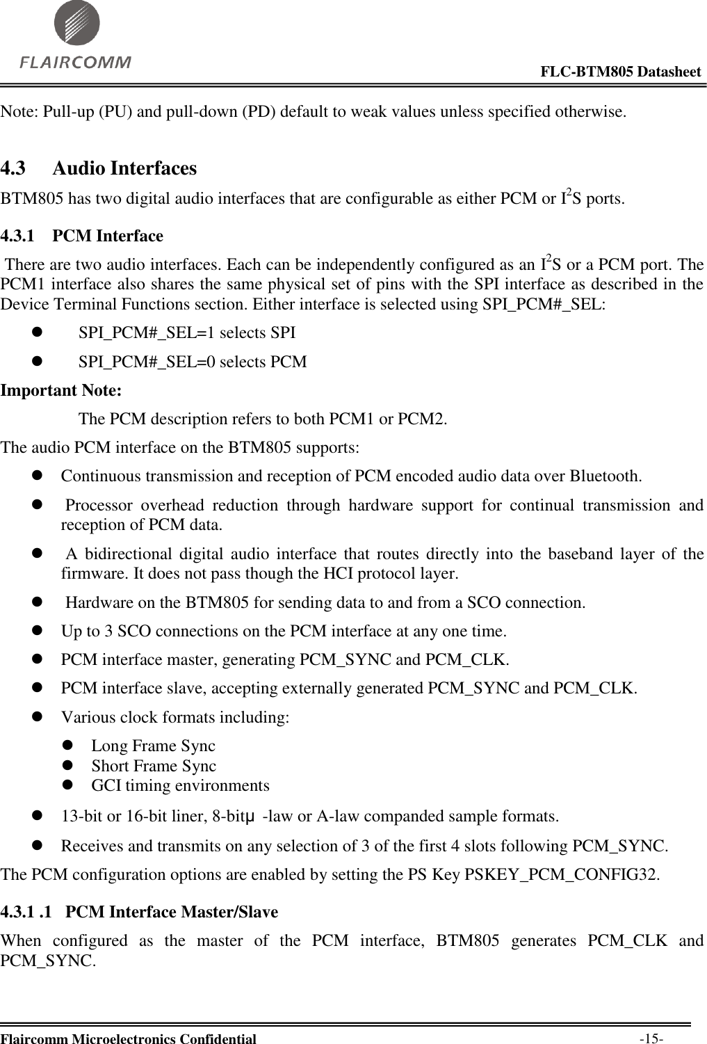
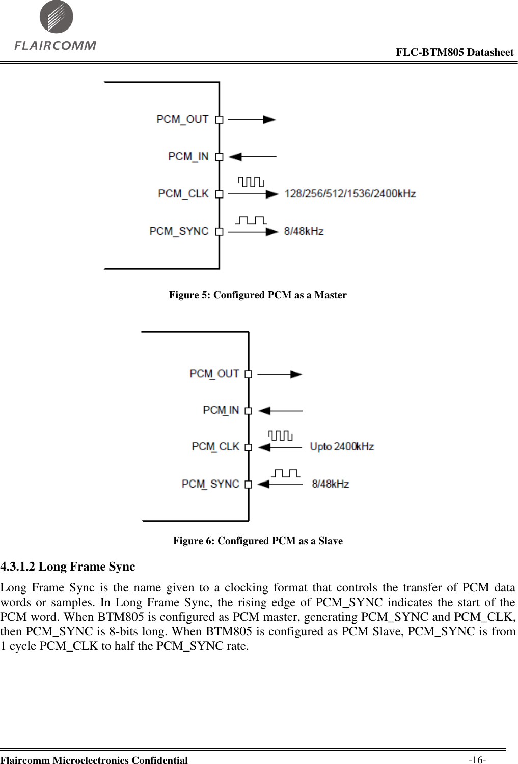
Flaircomm Microelectronics BTM805 Bluetooth module User Manual FLC BTM401 DS
Fujian Flaircomm Microelectronics,Inc. Bluetooth module FLC BTM401 DS
UserManual.wiki
>
Flaircomm Microelectronics
>
BTM805 User Manual
User Manual
Navigation menu
Upload a User Manual
Namespaces
Wiki Guide
HTML
PDF
Info
Views
User Manual
Discussion / Help
Navigation
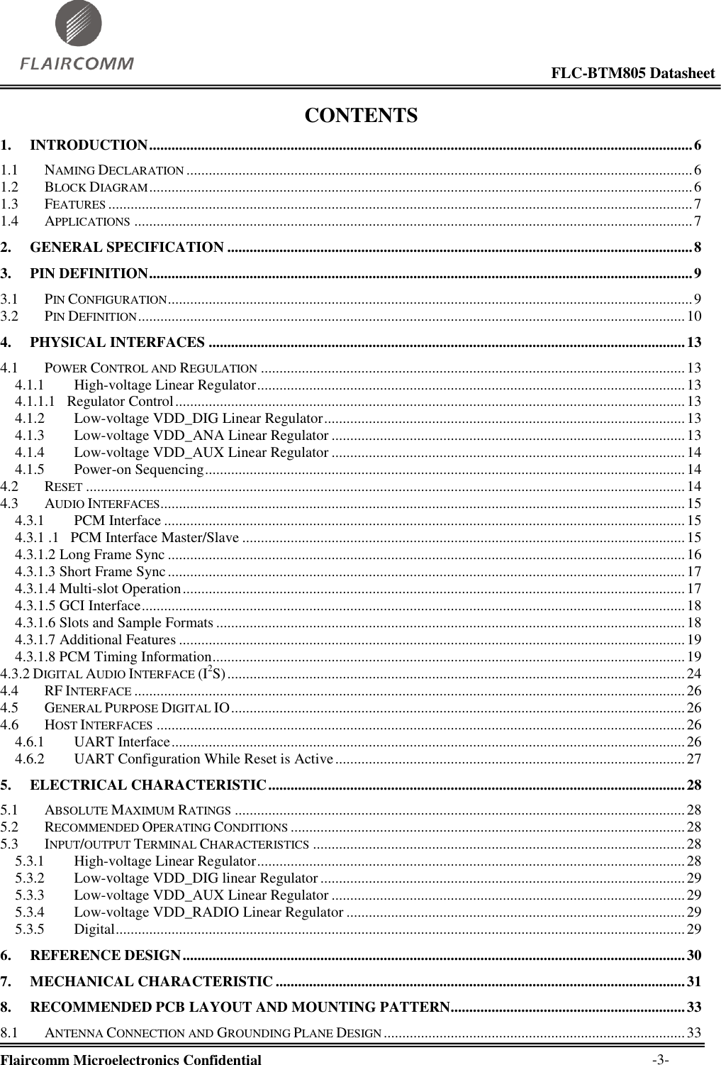
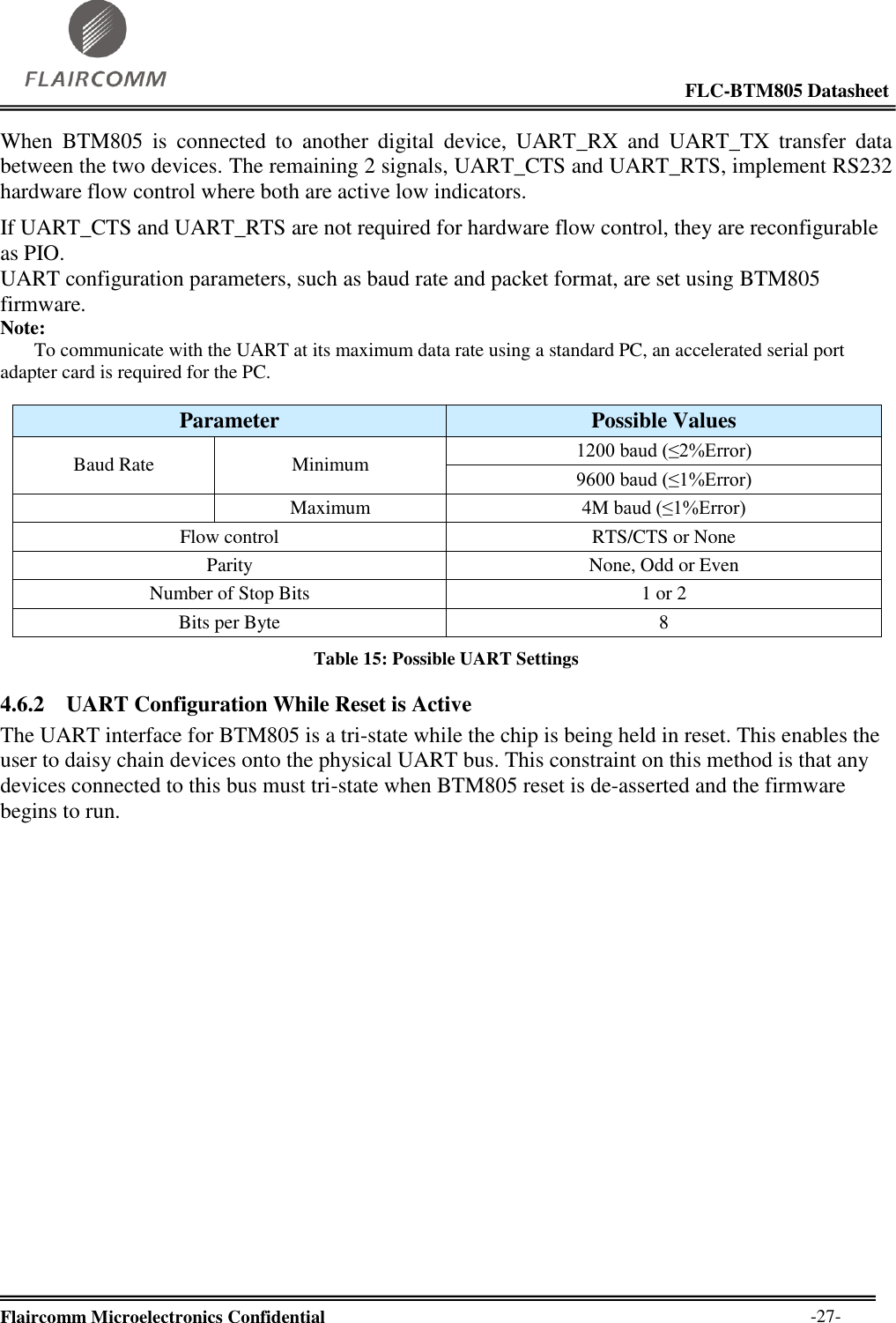
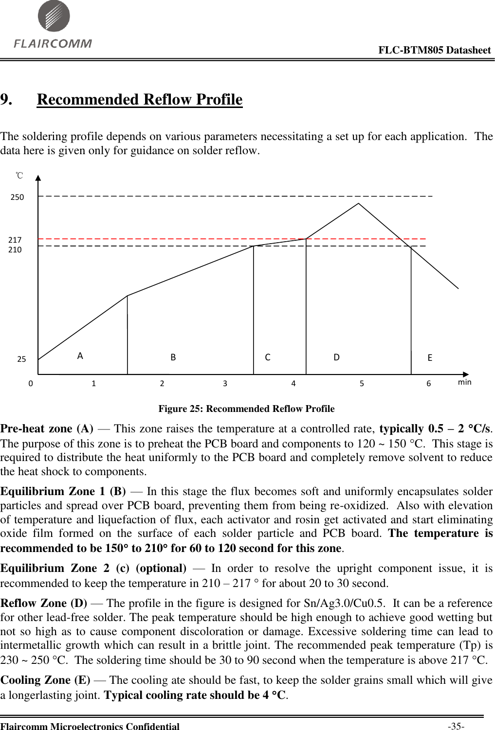
![FLC-BTM805 Datasheet Flaircomm Microelectronics Confidential -11- 11 VDD_PADS VDD Positive supply for all other digital input/output ports including PIO[6.0] and both PCMs 12 VREG_EN RST# Input with strong internal pull-down 1. Active low reset ; 2. Take high to enable internal regulators 13 VDD_IN Power supply Input to internal high-voltage regulator 14 VREG_OUT_HV Analogue regulator output Out from internal high-voltage regulator and input to low-voltage regulators 15 UART_TX Bi-directional, tristate, with weak internal pull-up UART data output, active high 16 UART_RX Input with weak internal pull-up UART data input, active high 17 UART_RTS Bi-directional input, with weak internal pull-up UART request to send, active low 18 UART_CTS Input, with weak internal pull-up UART clear to send, active low 19 VDD_RADIO Power supply decoupler Connect a 2.2uF caps on this pin 20 SPI_PCM#_SEL Input with internal pull down SPI / PCM selection High – SPI is selected Low – PCM is selected 21 PCM_IN/ SPI_MOSI / PIO[21] Input, tristate, with weak internal pull-down PCM synchronous data input SPI data input Programmable input/output line 22 PCM_CLK/ SPI_CLK/ PIO[24] Bidirectional, tristate, with weak internal pull-down PCM synchronous data clock SPI clock Programmable input/output line 23 PCM_SYNC/ SPI_CS#/ PIO[23] Bidirectional, tristate, with weak internal pull-down PCM synchronous data sync SPI chip select, active low Programmable input/output line 24 PCM_OUT/ SPI_MISO/ PIO[22] Output, tri-state, with weak internal pull-down PCM synchronous data output SPI data output Programmable input/output line 25 GND Ground Ground 26 GND Ground Ground 27 GND Ground Ground 28 GND Ground Ground Table 3: BTM805CL2A Pin Definition BTM805CL2B Pin Definition: Pin Symbol I/O Type Description 1 NC - Not in use 2 GND Ground Ground 3 VDD_AUX Analogue Regulator decoupler 2.2uF cap connect to this pin 4 PIO0 Bi-directional with programmable strength internal pull-up/down Programmable input/output line 5 PIO3 Bi-directional with programmable strength internal pull-up/down Programmable input/output line](https://usermanual.wiki/Flaircomm-Microelectronics/BTM805/User-Guide-1863209-Page-11.png)
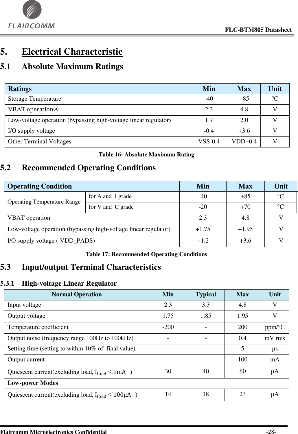
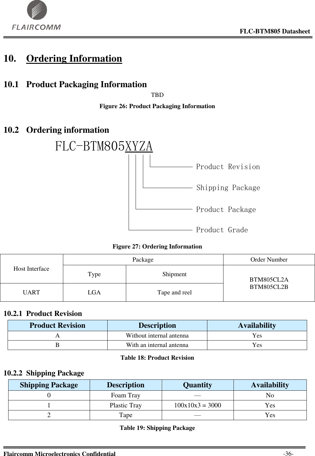
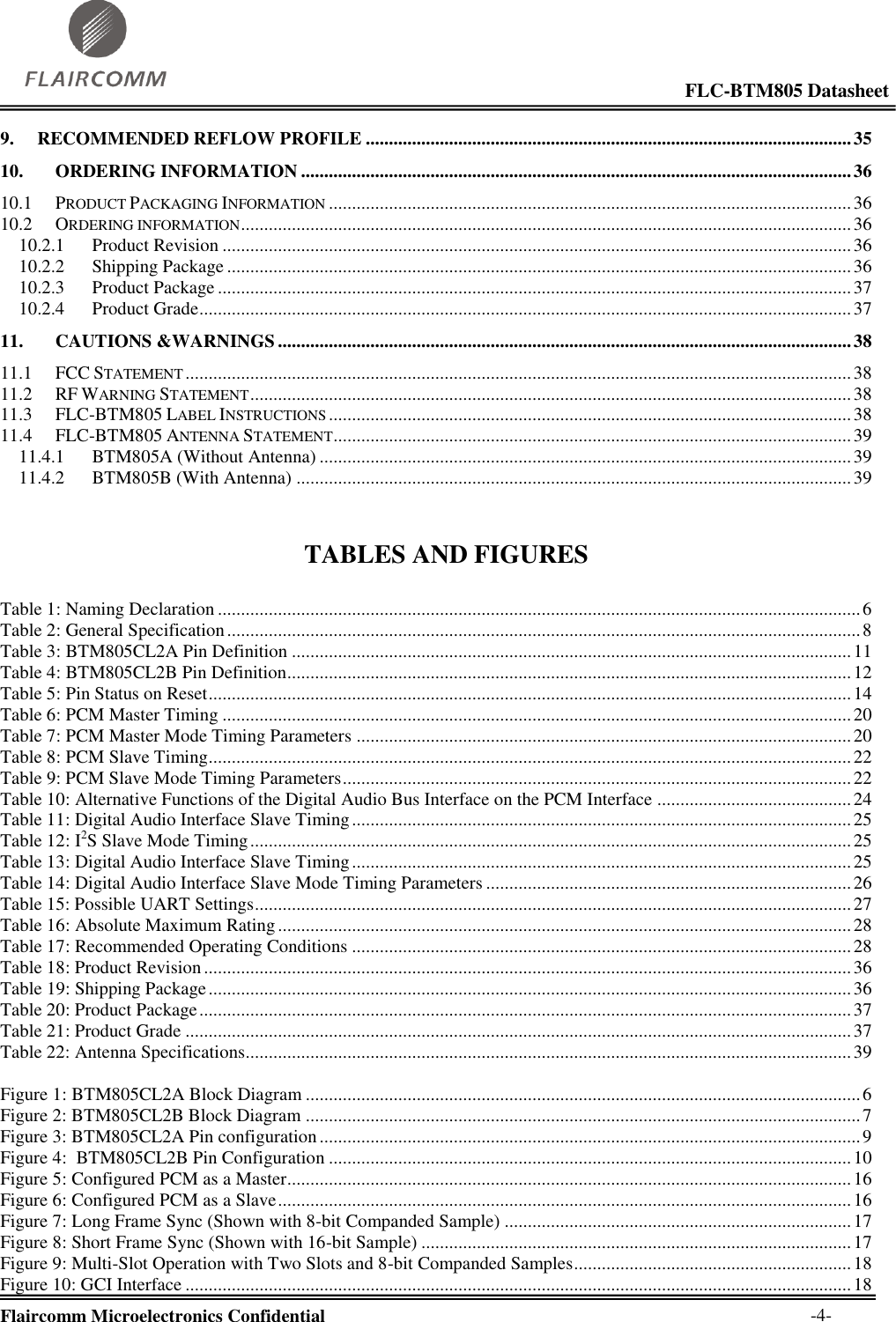
![FLC-BTM805 Datasheet Flaircomm Microelectronics Confidential -12- 6 PIO1 Bi-directional with programmable strength internal pull-up/down Programmable input/output line 7 VDD_DIG Digital Regulator decoupler 2.2uF cap connect to this pin 8 PIO4 Bi-directional with programmable strength internal pull-up/down Programmable input/output line 9 PIO2 Bi-directional with programmable strength internal pull-up/down Programmable input/output line 10 PIO5 Bi-directional with programmable strength internal pull-up/down Programmable input/output line 11 VDD_PADS VDD Positive supply for all other digital input/output ports including PIO[6.0] and both PCMs 12 VREG_EN RST# Input with strong internal pull-down 3. Active low reset ; 4. Take high to enable internal regulators 13 VDD_IN Power supply Input to internal high-voltage regulator 14 VREG_OUT_HV Analogue regulator output Out from internal high-voltage regulator and input to low-voltage regulators 15 UART_TX Bi-directional, tristate, with weak internal pull-up UART data output, active high 16 UART_RX Input with weak internal pull-up UART data input, active high 17 UART_RTS Bi-directional input, with weak internal pull-up UART request to send, active low 18 UART_CTS Input, with weak internal pull-up UART clear to send, active low 19 VDD_RADIO Power supply decoupler Connect a 2.2uF caps on this pin 20 SPI_PCM#_SEL Input with internal pull down SPI / PCM selection High – SPI is selected Low – PCM is selected 21 PCM_IN/ SPI_MOSI / PIO[21] Input, tristate, with weak internal pull-down PCM synchronous data input SPI data input Programmable input/output line 22 PCM_CLK/ SPI_CLK/ PIO[24] Bidirectional, tristate, with weak internal pull-down PCM synchronous data clock SPI clock Programmable input/output line 23 PCM_SYNC/ SPI_CS#/ PIO[23] Bidirectional, tristate, with weak internal pull-down PCM synchronous data sync SPI chip select, active low Programmable input/output line 24 PCM_OUT/ SPI_MISO/ PIO[22] Output, tri-state, with weak internal pull-down PCM synchronous data output SPI data output Programmable input/output line 25 GND Ground Ground 26 GND Ground Ground 27 GND Ground Ground 28 GND Ground Ground Table 4: BTM805CL2B Pin Definition](https://usermanual.wiki/Flaircomm-Microelectronics/BTM805/User-Guide-1863209-Page-12.png)
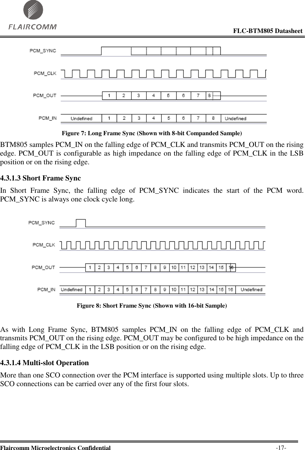
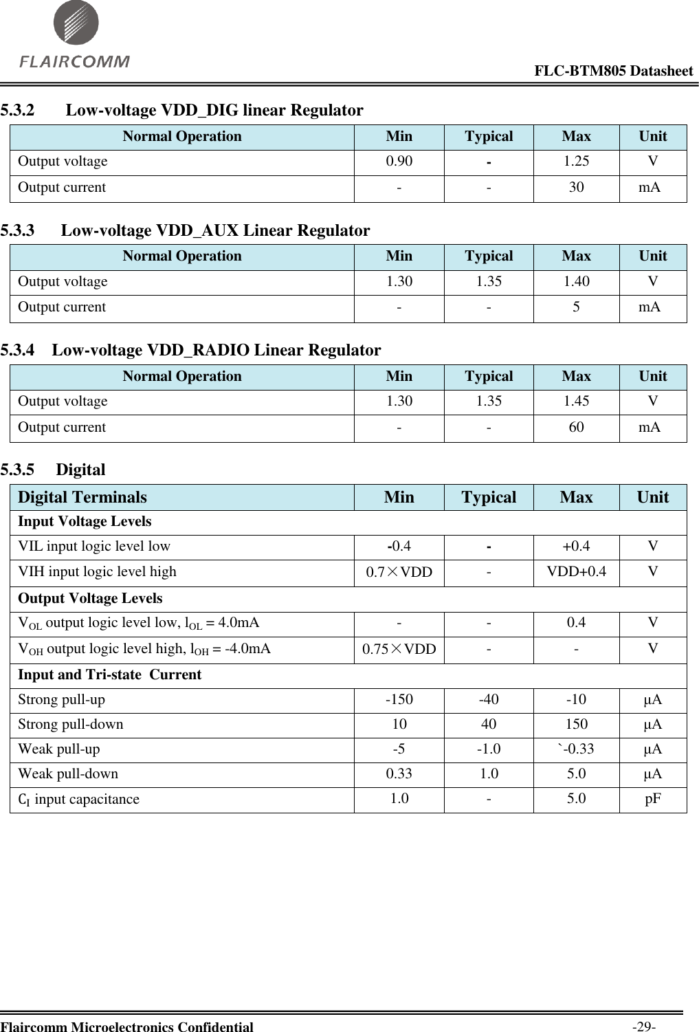
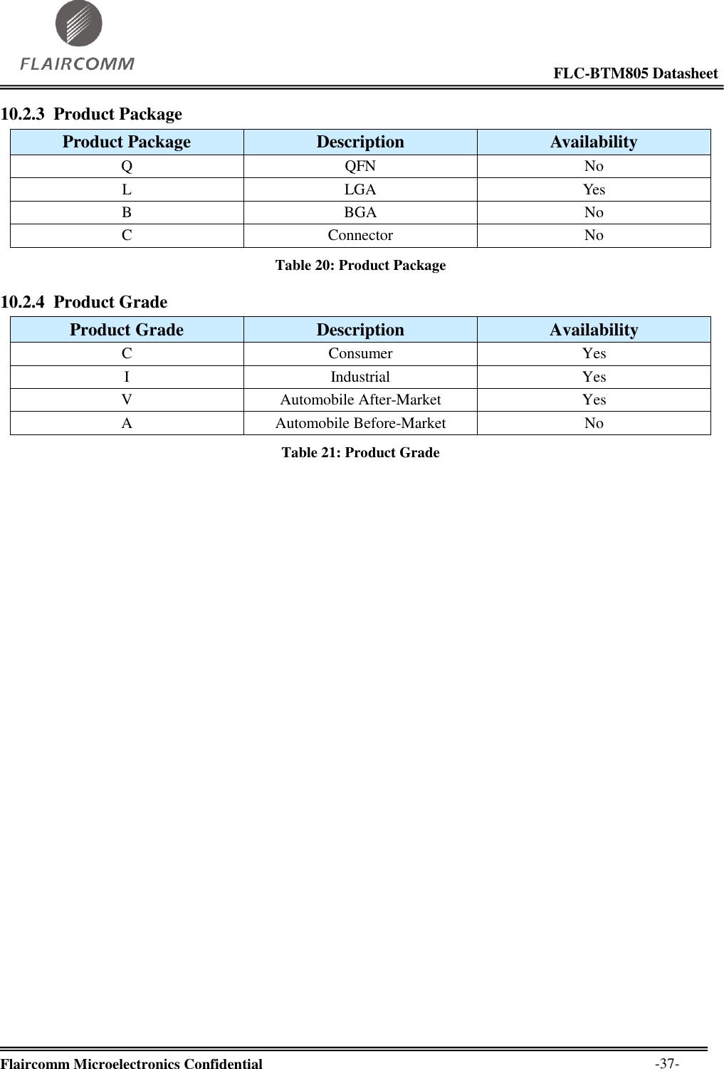
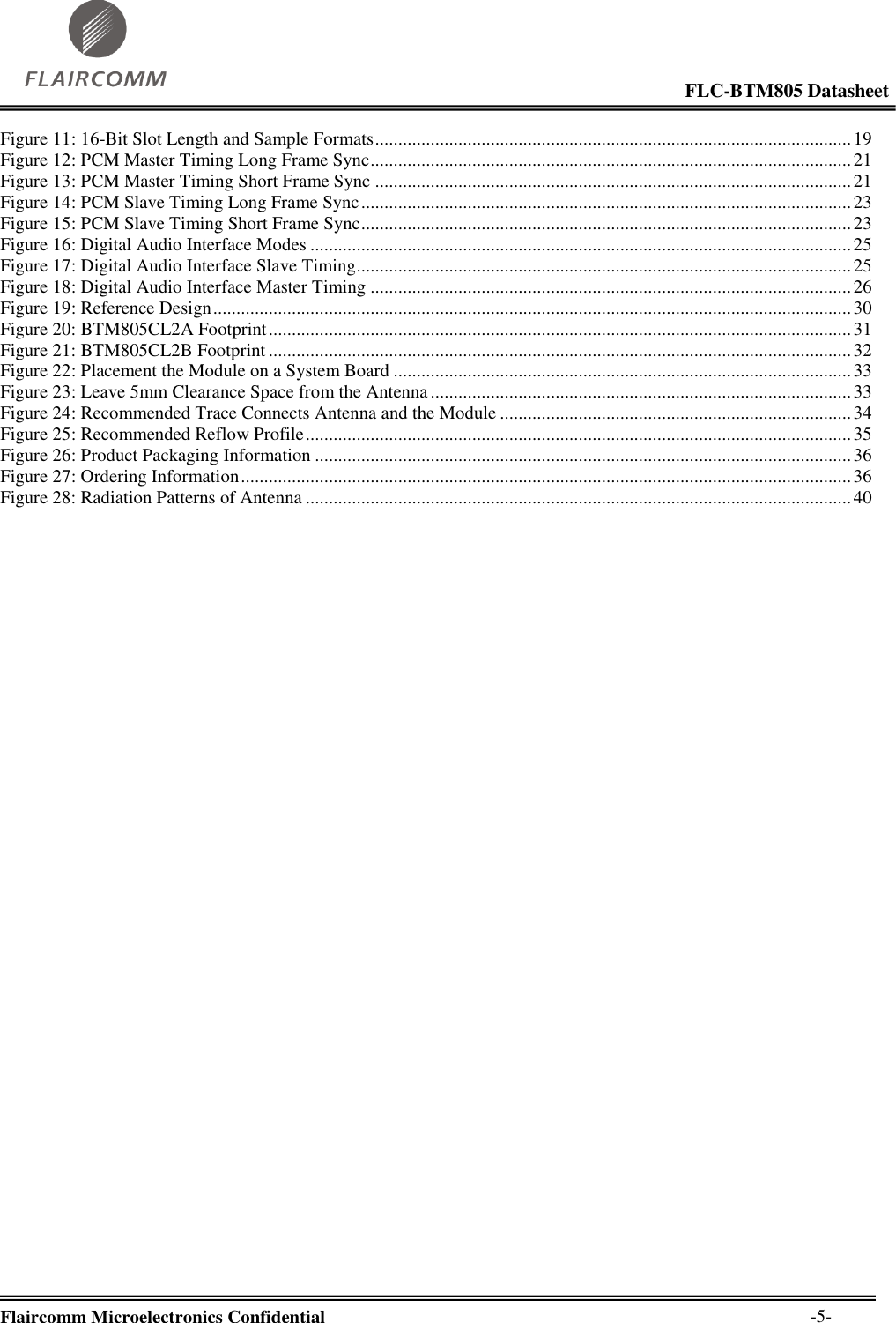
![FLC-BTM805 Datasheet Flaircomm Microelectronics Confidential -14- 4.1.4 Low-voltage VDD_AUX Linear Regulator The on-board low-voltage VDD_AUX Regulator powers BTM805 1.35V VDD_AUX supply. The regulator is controlled by the firmware. 4.1.5 Power-on Sequencing BTM805 does not have any strict relative timing requirements for clock and power supply sequencing during reset or power-on. Follow this sequence of operation to ensure that the initial cold boot is completed successfully: 1、All external power supplies should be stable. 2、VREG_EN_RST# should be driven high. It is then possible to establish host communications with the CRS8811 in order to set further configuration values. When you have set configuration values, perform a warm reset so that they take effect and normal radio operation can begin. 4.2 Reset BTM805 the reset function is internally tied to the VREG_EN_RST# pin. The BTM805 may be reset from several sources: VREG_EN_RST# pin Power-on reset A UART break character Via a software-configured watching timer The VREG_EN_RST# pin is an active low reset. To ensure a full reset the reset signal should be asserted for a period greater than 5ms. A warm reset function is also available under software control. After a warm reset the RAM data remains available. Pin Name / Group I/O Type No Core Voltage Reset Full Chip Reset VREG_EN_RST# Digital input Strong pull-down N/A SPI_CLK / PCM_CLK / PIO[24] Digital bidirectional tristated Weak pull-down Weak pull-down SPI_CS# / PCM_SYNC / PIO[23] Digital bidirectional tristated Weak pull-up (SPI) Weak pull-down (PCM) Weak pull-up (SPI) Weak pull-down (PCM / PIO) SPI_MISO / PCM_OUT / PIO[22] Digital output tristated Weak pull-down Weak pull-down SPI_MOSI / PCM_IN / PIO[21] Digital input Weak pull-down Weak pull-down PIO[5:0] Digital bidirectional tristated Weak pull-down Weak pull-down Table 5: Pin Status on Reset](https://usermanual.wiki/Flaircomm-Microelectronics/BTM805/User-Guide-1863209-Page-14.png)