Flaircomm Microelectronics BTM805 Bluetooth module User Manual FLC BTM401 DS
Fujian Flaircomm Microelectronics,Inc. Bluetooth module FLC BTM401 DS
User Manual

FLC-BTM805 Datasheet
Flaircomm Microelectronics Confidential
-1-
FLC-BTM805
Datasheet
Document Type: Bluetooth Module Datasheet
Document Number: FLC-BTM805-DS
Document Version: V1.6
Release Date: 2012/12/18
Copyright 2012~ 2014 by Flaircomm Microelectronics Inc., All Right Reserved
Without written permission from Flaircomm Microelectronics Inc., reproduction, transfer, distribution or
storage of part or all of the contents in this document in any form is prohibited
FLC-BTM805 Datasheet
Flaircomm Microelectronics Confidential
-2-
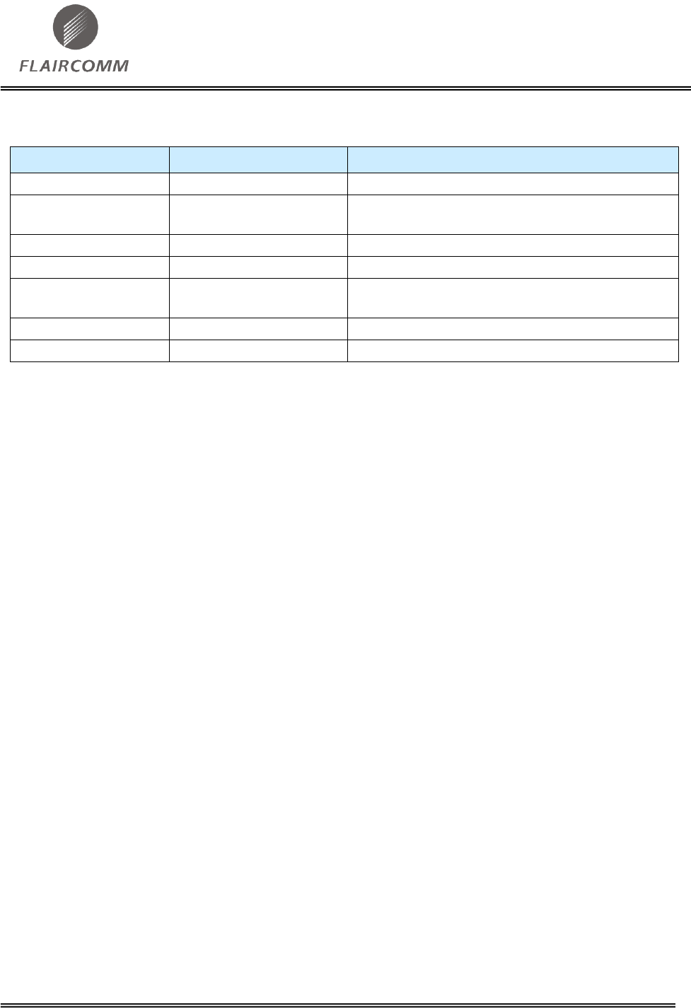
Release Record
Version
Release Date
Comments
1.0
2012/6/26
Release
1.1
2012/9/6
Modify operating temperature. Add BT/CE/FCC
logo. Add Cautions & Warnings.
1.2
2012/9/24
Modify sensitivity, weight and working current.
1.3
2012/11/2
Add FLC-BTM805 Antenna Statement.
1.4
2012/11/22
Small modification about Antenna Statement and
Label Instructions.
1.5
2012/11/27
Add module weight.
1.6
2012/12/18
Modify RF TX Power and FCC Statement.

FLC-BTM805 Datasheet
Flaircomm Microelectronics Confidential
-3-
CONTENTS
1. INTRODUCTION .................................................................................................................................................. 6
1.1 NAMING DECLARATION ........................................................................................................................................ 6
1.2 BLOCK DIAGRAM .................................................................................................................................................. 6
1.3 FEATURES ............................................................................................................................................................. 7
1.4 APPLICATIONS ...................................................................................................................................................... 7
2. GENERAL SPECIFICATION ............................................................................................................................. 8
3. PIN DEFINITION .................................................................................................................................................. 9
3.1 PIN CONFIGURATION ............................................................................................................................................. 9
3.2 PIN DEFINITION ................................................................................................................................................... 10
4. PHYSICAL INTERFACES ................................................................................................................................ 13
4.1 POWER CONTROL AND REGULATION .................................................................................................................. 13
4.1.1 High-voltage Linear Regulator ................................................................................................................... 13
4.1.1.1 Regulator Control ......................................................................................................................................... 13
4.1.2 Low-voltage VDD_DIG Linear Regulator ................................................................................................. 13
4.1.3 Low-voltage VDD_ANA Linear Regulator ............................................................................................... 13
4.1.4 Low-voltage VDD_AUX Linear Regulator ............................................................................................... 14
4.1.5 Power-on Sequencing ................................................................................................................................. 14
4.2 RESET ................................................................................................................................................................. 14
4.3 AUDIO INTERFACES............................................................................................................................................. 15
4.3.1 PCM Interface ............................................................................................................................................ 15
4.3.1 .1 PCM Interface Master/Slave ....................................................................................................................... 15
4.3.1.2 Long Frame Sync ........................................................................................................................................... 16
4.3.1.3 Short Frame Sync ........................................................................................................................................... 17
4.3.1.4 Multi-slot Operation ....................................................................................................................................... 17
4.3.1.5 GCI Interface .................................................................................................................................................. 18
4.3.1.6 Slots and Sample Formats .............................................................................................................................. 18
4.3.1.7 Additional Features ........................................................................................................................................ 19
4.3.1.8 PCM Timing Information ............................................................................................................................... 19
4.3.2 DIGITAL AUDIO INTERFACE (I2S) ........................................................................................................................... 24
4.4 RF INTERFACE .................................................................................................................................................... 26
4.5 GENERAL PURPOSE DIGITAL IO .......................................................................................................................... 26
4.6 HOST INTERFACES .............................................................................................................................................. 26
4.6.1 UART Interface .......................................................................................................................................... 26
4.6.2 UART Configuration While Reset is Active .............................................................................................. 27
5. ELECTRICAL CHARACTERISTIC ................................................................................................................ 28
5.1 ABSOLUTE MAXIMUM RATINGS ......................................................................................................................... 28
5.2 RECOMMENDED OPERATING CONDITIONS .......................................................................................................... 28
5.3 INPUT/OUTPUT TERMINAL CHARACTERISTICS .................................................................................................... 28
5.3.1 High-voltage Linear Regulator ................................................................................................................... 28
5.3.2 Low-voltage VDD_DIG linear Regulator .................................................................................................. 29
5.3.3 Low-voltage VDD_AUX Linear Regulator ............................................................................................... 29
5.3.4 Low-voltage VDD_RADIO Linear Regulator ........................................................................................... 29
5.3.5 Digital ......................................................................................................................................................... 29
6. REFERENCE DESIGN ....................................................................................................................................... 30
7. MECHANICAL CHARACTERISTIC .............................................................................................................. 31
8. RECOMMENDED PCB LAYOUT AND MOUNTING PATTERN............................................................... 33
8.1 ANTENNA CONNECTION AND GROUNDING PLANE DESIGN ................................................................................. 33

FLC-BTM805 Datasheet
Flaircomm Microelectronics Confidential
-4-
9. RECOMMENDED REFLOW PROFILE ......................................................................................................... 35
10. ORDERING INFORMATION ....................................................................................................................... 36
10.1 PRODUCT PACKAGING INFORMATION ................................................................................................................. 36
10.2 ORDERING INFORMATION .................................................................................................................................... 36
10.2.1 Product Revision ........................................................................................................................................ 36
10.2.2 Shipping Package ....................................................................................................................................... 36
10.2.3 Product Package ......................................................................................................................................... 37
10.2.4 Product Grade ............................................................................................................................................. 37
11. CAUTIONS &WARNINGS ............................................................................................................................ 38
11.1 FCC STATEMENT ................................................................................................................................................ 38
11.2 RF WARNING STATEMENT .................................................................................................................................. 38
11.3 FLC-BTM805 LABEL INSTRUCTIONS ................................................................................................................. 38
11.4 FLC-BTM805 ANTENNA STATEMENT ................................................................................................................ 39
11.4.1 BTM805A (Without Antenna) ................................................................................................................... 39
11.4.2 BTM805B (With Antenna) ........................................................................................................................ 39
TABLES AND FIGURES
Table 1: Naming Declaration ........................................................................................................................................... 6
Table 2: General Specification ......................................................................................................................................... 8
Table 3: BTM805CL2A Pin Definition ......................................................................................................................... 11
Table 4: BTM805CL2B Pin Definition .......................................................................................................................... 12
Table 5: Pin Status on Reset ........................................................................................................................................... 14
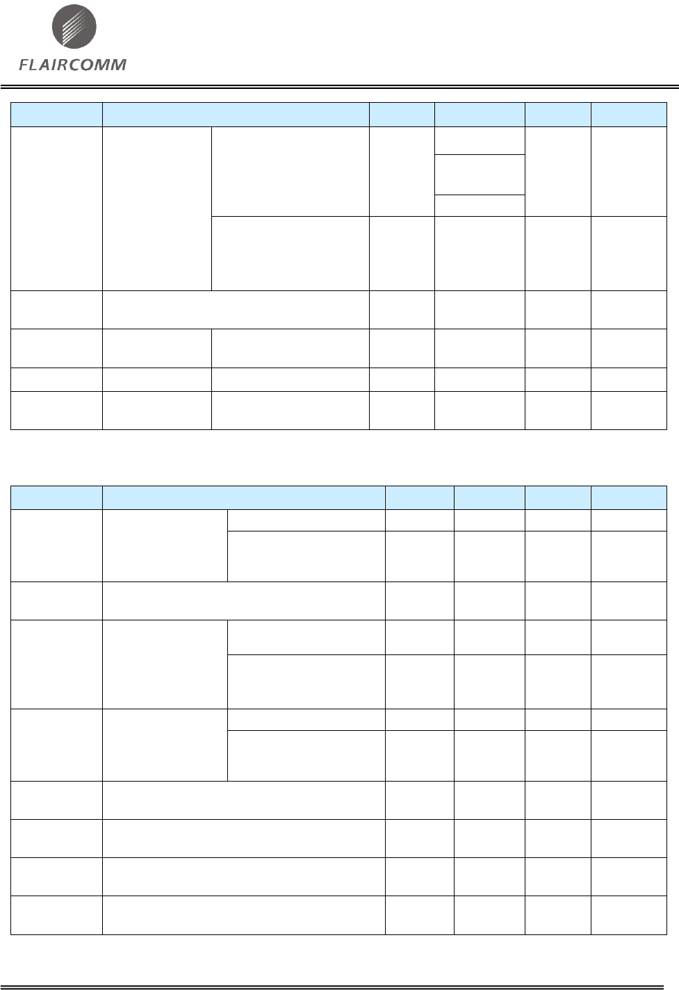
Table 6: PCM Master Timing ........................................................................................................................................ 20
Table 7: PCM Master Mode Timing Parameters ........................................................................................................... 20
Table 8: PCM Slave Timing ........................................................................................................................................... 22
Table 9: PCM Slave Mode Timing Parameters .............................................................................................................. 22
Table 10: Alternative Functions of the Digital Audio Bus Interface on the PCM Interface .......................................... 24
Table 11: Digital Audio Interface Slave Timing ............................................................................................................ 25
Table 12: I2S Slave Mode Timing .................................................................................................................................. 25
Table 13: Digital Audio Interface Slave Timing ............................................................................................................ 25
Table 14: Digital Audio Interface Slave Mode Timing Parameters ............................................................................... 26
Table 15: Possible UART Settings ................................................................................................................................. 27
Table 16: Absolute Maximum Rating ............................................................................................................................ 28
Table 17: Recommended Operating Conditions ............................................................................................................ 28
Table 18: Product Revision ............................................................................................................................................ 36
Table 19: Shipping Package ........................................................................................................................................... 36
Table 20: Product Package ............................................................................................................................................. 37
Table 21: Product Grade ................................................................................................................................................ 37
Table 22: Antenna Specifications................................................................................................................................... 39
Figure 1: BTM805CL2A Block Diagram ........................................................................................................................ 6
Figure 2: BTM805CL2B Block Diagram ........................................................................................................................ 7
Figure 3: BTM805CL2A Pin configuration ..................................................................................................................... 9
Figure 4: BTM805CL2B Pin Configuration ................................................................................................................. 10
Figure 5: Configured PCM as a Master .......................................................................................................................... 16
Figure 6: Configured PCM as a Slave ............................................................................................................................ 16
Figure 7: Long Frame Sync (Shown with 8-bit Companded Sample) ........................................................................... 17
Figure 8: Short Frame Sync (Shown with 16-bit Sample) ............................................................................................. 17
Figure 9: Multi-Slot Operation with Two Slots and 8-bit Companded Samples ............................................................ 18
Figure 10: GCI Interface ................................................................................................................................................ 18

FLC-BTM805 Datasheet
Flaircomm Microelectronics Confidential
-5-
Figure 11: 16-Bit Slot Length and Sample Formats ....................................................................................................... 19
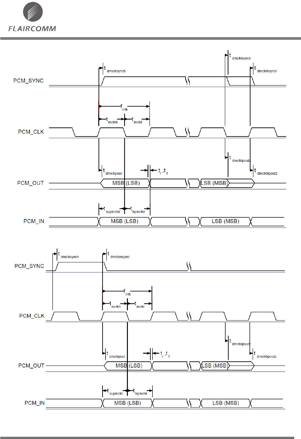
Figure 12: PCM Master Timing Long Frame Sync ........................................................................................................ 21
Figure 13: PCM Master Timing Short Frame Sync ....................................................................................................... 21
Figure 14: PCM Slave Timing Long Frame Sync .......................................................................................................... 23
Figure 15: PCM Slave Timing Short Frame Sync .......................................................................................................... 23
Figure 16: Digital Audio Interface Modes ..................................................................................................................... 25
Figure 17: Digital Audio Interface Slave Timing ........................................................................................................... 25
Figure 18: Digital Audio Interface Master Timing ........................................................................................................ 26
Figure 19: Reference Design .......................................................................................................................................... 30
Figure 20: BTM805CL2A Footprint .............................................................................................................................. 31
Figure 21: BTM805CL2B Footprint .............................................................................................................................. 32
Figure 22: Placement the Module on a System Board ................................................................................................... 33
Figure 23: Leave 5mm Clearance Space from the Antenna ........................................................................................... 33
Figure 24: Recommended Trace Connects Antenna and the Module ............................................................................ 34
Figure 25: Recommended Reflow Profile ...................................................................................................................... 35
Figure 26: Product Packaging Information .................................................................................................................... 36
Figure 27: Ordering Information .................................................................................................................................... 36
Figure 28: Radiation Patterns of Antenna ...................................................................................................................... 40
FLC-BTM805 Datasheet
Flaircomm Microelectronics Confidential
-6-
1. Introduction
FLC-BTM805 is a dual-mode Bluetooth HCI module that allows OEM to add Bluetooth wireless
capability to their products. The module supports BT3.0-HS and BT4.0 (Bluetooth low energy) with
HCI interface that makes it simple to design into fully certified embedded Bluetooth solutions.
With FLC’s Bluetooth stack running on a host, designers can easily customize their applications to
support different Bluetooth profiles, such HS/HF, A2DP, AVRCP, OPP, DUN, SPP, and etc. The
module supports Bluetooth® Enhanced Data Rate (EDR) and delivers up to 3 Mbps data rate.
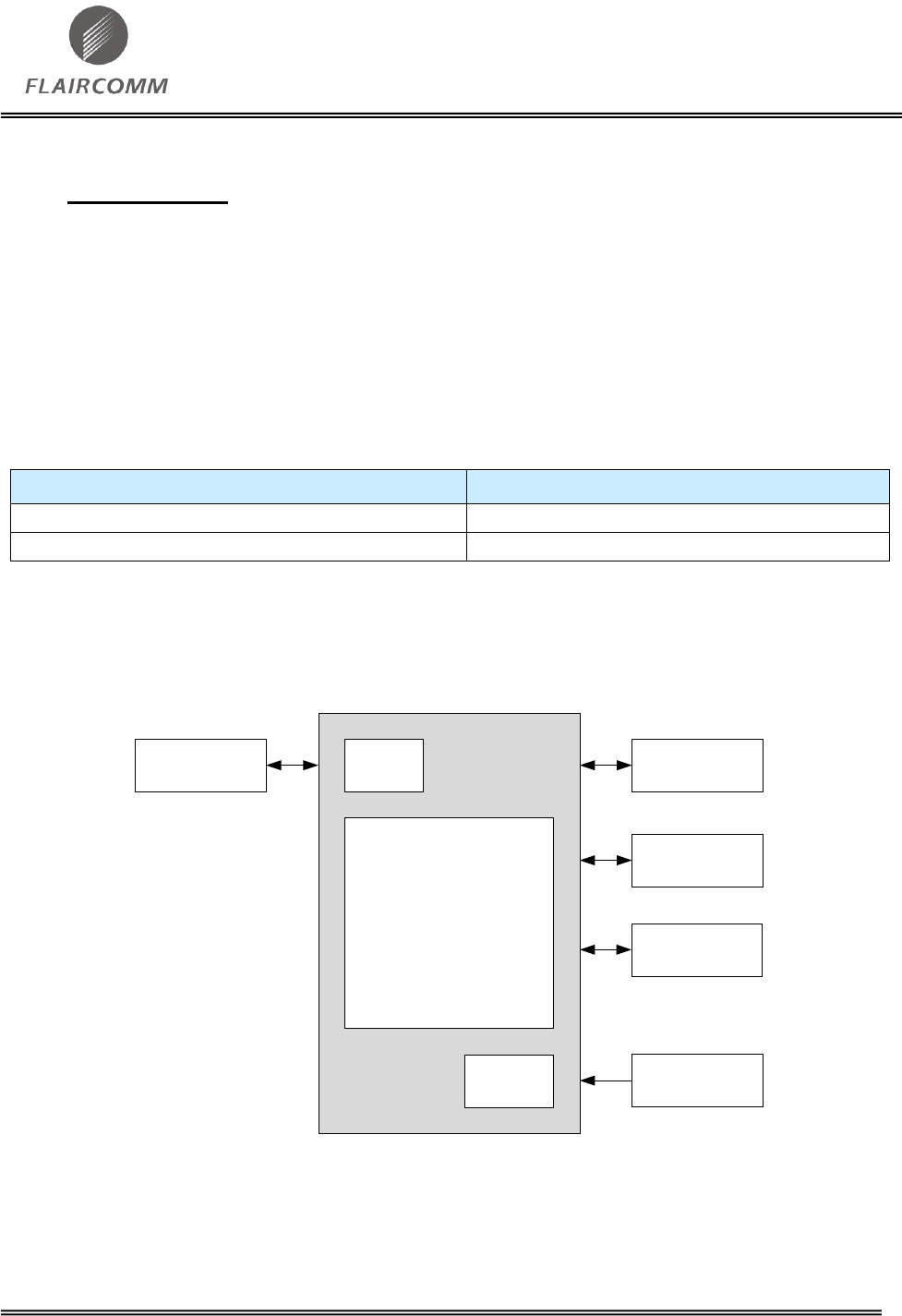
1.1 Naming Declaration
New Naming
Old Naming
FLC-BTM805CL2A
NA
FLC-BTM805CL2B
NA
Table 1: Naming Declaration
1.2 Block Diagram
UART
PIOsAntenna
Crystal
CSR8811
Filter
SPI / PCM
VDD
Figure 1: BTM805CL2A Block Diagram
FLC-BTM805 Datasheet
Flaircomm Microelectronics Confidential
-7-
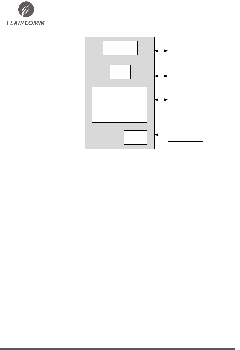
UART
PIOs
Crystal
CSR8811
Filter
SPI / PCM
VDD
Antenna
Figure 2: BTM805CL2B Block Diagram
1.3 Features
Fully qualified Bluetooth® v4.0 specification system
Dual-mode Bluetooth /Bluetooth low energy
Draft Bluetooth low energy HID boot mode support
Full-speed Bluetooth operation with full piconet and scatternet support
High speed UART interface
WLAN coexistence interface
Green (RoHS)
1.4 Applications
Feature phones, Smart phones
Personal Navigation Devices (PNDs)
Potable Media Players (PMPs)
M2M
Bluetooth low energy
FLC-BTM805 Datasheet
Flaircomm Microelectronics Confidential
-8-
2. General Specification
Bluetooth Specification
Standard
BT2.1+EDR, BT 3.0-HS, BT4.0 BLE
Frequency Band
2.402G ~ 2.480G
Maximum Data Rate
3Mbps
RF Input Impedance
50 ohms
Baseband TCXO
26MHz
Interface
UART, PIO, SPI, PCM/I2S/SPDIF
Sensitivity
-86dBm@0.1%BER
RF TX Power
8.5dBm(MAX)
Power
Supply Voltage
2.3 ~ 4.8V DC
Working Current
100mA (MAX)
Standby Current
——
Operating Environment
Temperature
-40ºC to +85ºC for A and I grade
-20ºC to +70ºC for V and C grade
Humidity
10%~90% Non-Condensing
Certifications
BQB/FCC/CE
Environmental
RoHS Compliant
Dimension and Weight
Dimension with Antenna
12mm x 7mm x 1.50mm
Dimension without Antenna
7mm x 7mm x 1.50mm
Weight with Antenna
~0.24g
Weight without Antenna
~0.18g
Table 2: General Specification
FLC-BTM805 Datasheet
Flaircomm Microelectronics Confidential
-9-
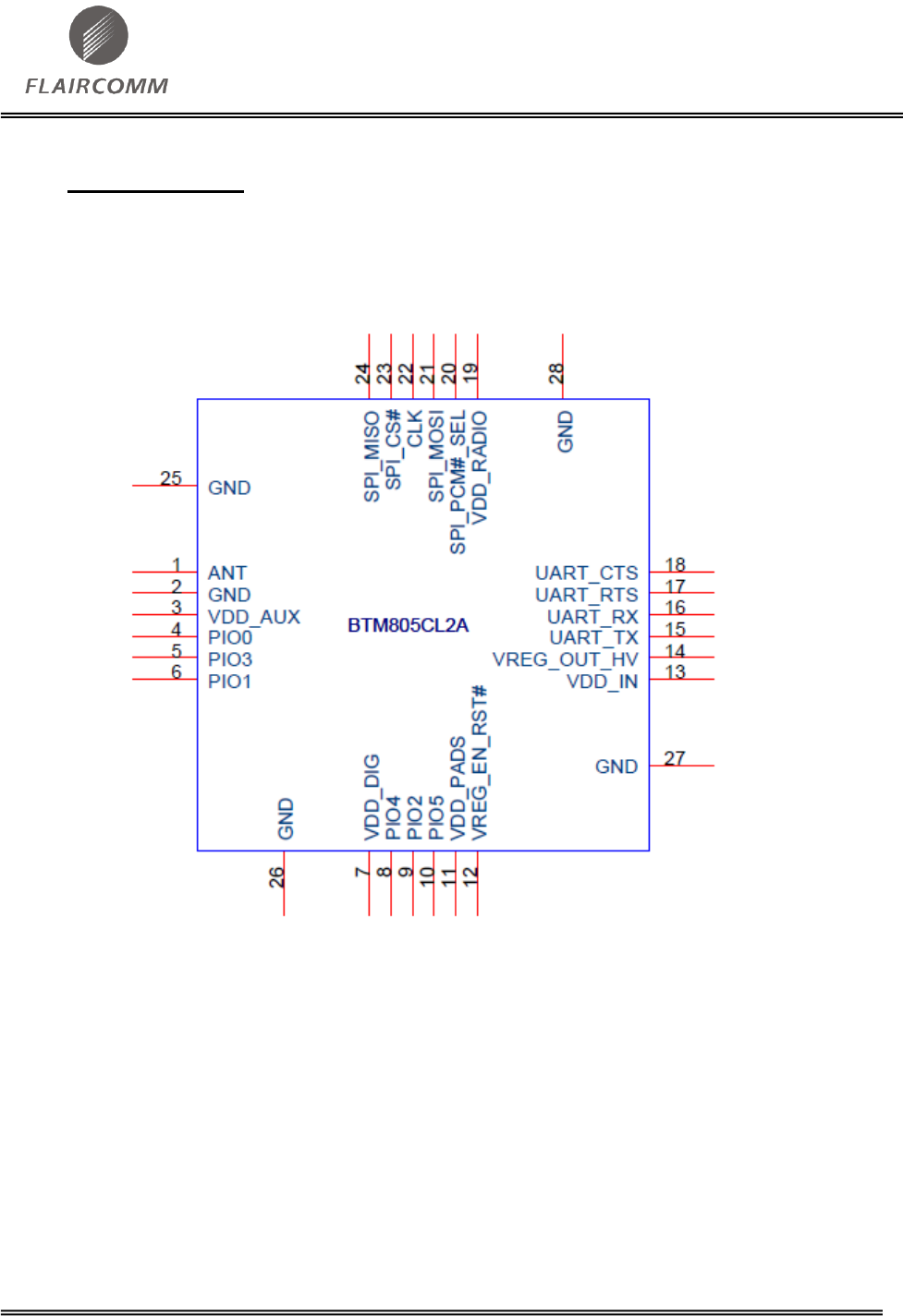
3. Pin Definition
3.1 Pin Configuration
Figure 3: BTM805CL2A Pin configuration
FLC-BTM805 Datasheet
Flaircomm Microelectronics Confidential
-10-
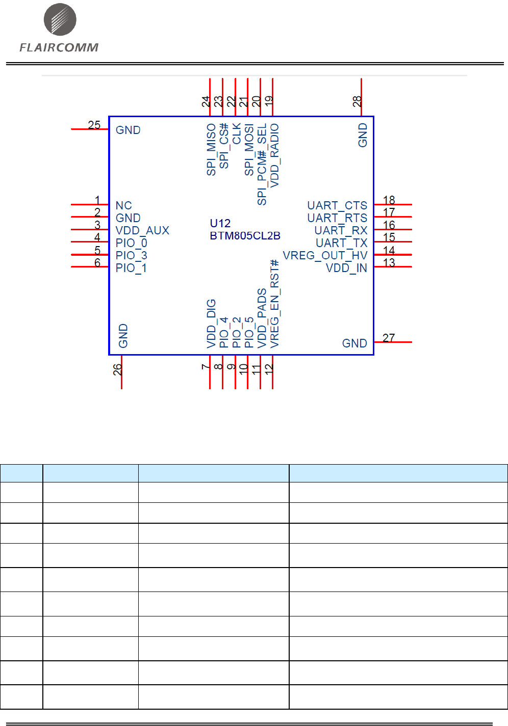
Figure 4: BTM805CL2B Pin Configuration
3.2 Pin Definition
BTM805CL2A Pin Definition:
Pin
Symbol
I/O Type
Description
1
ANT
RF
Antenna Port
2
GND
Ground
Ground
3
VDD_AUX
Analogue Regulator decoupler
2.2uF cap connect to this pin
4
PIO0
Bi-directional with programmable
strength internal pull-up/down
Programmable input/output line
5
PIO3
Bi-directional with programmable
strength internal pull-up/down
Programmable input/output line
6
PIO1
Bi-directional with programmable
strength internal pull-up/down
Programmable input/output line
7
VDD_DIG
Digital Regulator decoupler
2.2uF cap connect to this pin
8
PIO4
Bi-directional with programmable
strength internal pull-up/down
Programmable input/output line
9
PIO2
Bi-directional with programmable
strength internal pull-up/down
Programmable input/output line
10
PIO5
Bi-directional with programmable
strength internal pull-up/down
Programmable input/output line

FLC-BTM805 Datasheet
Flaircomm Microelectronics Confidential
-11-
11
VDD_PADS
VDD
Positive supply for all other digital input/output
ports including PIO[6.0] and both PCMs
12
VREG_EN RST#
Input with strong internal pull-
down
1. Active low reset ;
2. Take high to enable internal regulators
13
VDD_IN
Power supply
Input to internal high-voltage regulator
14
VREG_OUT_HV
Analogue regulator output
Out from internal high-voltage regulator and input
to low-voltage regulators
15
UART_TX
Bi-directional, tristate, with weak
internal pull-up
UART data output, active high
16
UART_RX
Input with weak internal pull-up
UART data input, active high
17
UART_RTS
Bi-directional input, with weak
internal pull-up
UART request to send, active low
18
UART_CTS
Input, with weak internal pull-up
UART clear to send, active low
19
VDD_RADIO
Power supply decoupler
Connect a 2.2uF caps on this pin
20
SPI_PCM#_SEL
Input with internal pull down
SPI / PCM selection
High – SPI is selected
Low – PCM is selected
21
PCM_IN/
SPI_MOSI /
PIO[21]
Input, tristate, with weak internal
pull-down
PCM synchronous data input
SPI data input
Programmable input/output line
22
PCM_CLK/
SPI_CLK/
PIO[24]
Bidirectional, tristate, with weak
internal pull-down
PCM synchronous data clock
SPI clock
Programmable input/output line
23
PCM_SYNC/
SPI_CS#/
PIO[23]
Bidirectional, tristate, with weak
internal pull-down
PCM synchronous data sync
SPI chip select, active low
Programmable input/output line
24
PCM_OUT/
SPI_MISO/
PIO[22]
Output, tri-state, with weak
internal pull-down
PCM synchronous data output
SPI data output
Programmable input/output line
25
GND
Ground
Ground
26
GND
Ground
Ground
27
GND
Ground
Ground
28
GND
Ground
Ground
Table 3: BTM805CL2A Pin Definition
BTM805CL2B Pin Definition:
Pin
Symbol
I/O Type
Description
1
NC
-
Not in use
2
GND
Ground
Ground
3
VDD_AUX
Analogue Regulator decoupler
2.2uF cap connect to this pin
4
PIO0
Bi-directional with programmable
strength internal pull-up/down
Programmable input/output line
5
PIO3
Bi-directional with programmable
strength internal pull-up/down
Programmable input/output line
FLC-BTM805 Datasheet
Flaircomm Microelectronics Confidential
-12-
6
PIO1
Bi-directional with programmable
strength internal pull-up/down
Programmable input/output line
7
VDD_DIG
Digital Regulator decoupler
2.2uF cap connect to this pin
8
PIO4
Bi-directional with programmable
strength internal pull-up/down
Programmable input/output line
9
PIO2
Bi-directional with programmable
strength internal pull-up/down
Programmable input/output line
10
PIO5
Bi-directional with programmable
strength internal pull-up/down
Programmable input/output line
11
VDD_PADS
VDD
Positive supply for all other digital input/output
ports including PIO[6.0] and both PCMs
12
VREG_EN RST#
Input with strong internal pull-
down
3. Active low reset ;
4. Take high to enable internal regulators
13
VDD_IN
Power supply
Input to internal high-voltage regulator
14
VREG_OUT_HV
Analogue regulator output
Out from internal high-voltage regulator and input
to low-voltage regulators
15
UART_TX
Bi-directional, tristate, with weak
internal pull-up
UART data output, active high
16
UART_RX
Input with weak internal pull-up
UART data input, active high
17
UART_RTS
Bi-directional input, with weak
internal pull-up
UART request to send, active low
18
UART_CTS
Input, with weak internal pull-up
UART clear to send, active low
19
VDD_RADIO
Power supply decoupler
Connect a 2.2uF caps on this pin
20
SPI_PCM#_SEL
Input with internal pull down
SPI / PCM selection
High – SPI is selected
Low – PCM is selected
21
PCM_IN/
SPI_MOSI /
PIO[21]
Input, tristate, with weak internal
pull-down
PCM synchronous data input
SPI data input
Programmable input/output line
22
PCM_CLK/
SPI_CLK/
PIO[24]
Bidirectional, tristate, with weak
internal pull-down
PCM synchronous data clock
SPI clock
Programmable input/output line
23
PCM_SYNC/
SPI_CS#/
PIO[23]
Bidirectional, tristate, with weak
internal pull-down
PCM synchronous data sync
SPI chip select, active low
Programmable input/output line
24
PCM_OUT/
SPI_MISO/
PIO[22]
Output, tri-state, with weak
internal pull-down
PCM synchronous data output
SPI data output
Programmable input/output line
25
GND
Ground
Ground
26
GND
Ground
Ground
27
GND
Ground
Ground
28
GND
Ground
Ground
Table 4: BTM805CL2B Pin Definition

FLC-BTM805 Datasheet
Flaircomm Microelectronics Confidential
-13-
4. Physical Interfaces
4.1 Power Control and Regulation
Four regulators are integrated in this product.
The high-voltage regulator generates the main 1.8V rail from the VDD_IN. This then supplies 3
lower voltage linear regulators:
A programmable low-voltage regulator to supply the 0.90V to 1.25V digital supply, VDD_DIG
A low-voltage regulator to supply the 1.35V VDD_ RADIO rail
An always-on regulator to supply 1.35V to auxiliary and reference circuitry, VDD_AUX
4.1.1 High-voltage Linear Regulator
A minimum 1.5uF capacitor must be connected to the VREG_OUT_HV pin. Low ESR capacitors
such as multilayer ceramic types should be used.
BTM805 recommends that the supplies are all powered at the same time. The order of powering the
supplies relative to the other I/O supply (VDD_PADS) is not important. If the I/O supply is powered
before the supplies all digital I/Os will have a weak pull-down irrespective of the reset state.
4.1.1.1 Regulator Control
The regulator is enabled by taking the VREG_EN_RST# pin above 1V. The regulator can be
controlled by the software.
The VREG_EN_RST# is also connected internally to the reset function.
VREG_EN_RST# pin is pulled down internally.
4.1.2 Low-voltage VDD_DIG Linear Regulator
The on-chip low-voltage VDD_DIG Regulator powers BTM805 digital circuits.
A minimum 1.5uF capacitor must be connected to the VDD_DIG pin. Low ESR capacitors such as
multilayer ceramic types should be used.
The regulator enable and output voltage is controlled by the firmware.
4.1.3 Low-voltage VDD_ANA Linear Regulator
The on-chip low-voltage VDD_ANA Linear Regulator powers the internal radio circuits of BTM805.
A minimum 1.5uF capacitor must be connected to the VDD_ANA pin. Low ESR capacitors such as
multilayer ceramic types should be used.
The regulator is controlled by the firmware. The regulator is disabled when the device is in deep
sleep mode or reset.
FLC-BTM805 Datasheet
Flaircomm Microelectronics Confidential
-14-
4.1.4 Low-voltage VDD_AUX Linear Regulator
The on-board low-voltage VDD_AUX Regulator powers BTM805 1.35V VDD_AUX supply.
The regulator is controlled by the firmware.
4.1.5 Power-on Sequencing
BTM805 does not have any strict relative timing requirements for clock and power supply
sequencing during reset or power-on. Follow this sequence of operation to ensure that the initial cold
boot is completed successfully:
1、All external power supplies should be stable.
2、VREG_EN_RST# should be driven high.
It is then possible to establish host communications with the CRS8811 in order to set further
configuration values. When you have set configuration values, perform a warm reset so that they
take effect and normal radio operation can begin.
4.2 Reset
BTM805 the reset function is internally tied to the VREG_EN_RST# pin. The BTM805 may be
reset from several sources:
VREG_EN_RST# pin
Power-on reset
A UART break character
Via a software-configured watching timer
The VREG_EN_RST# pin is an active low reset. To ensure a full reset the reset signal should be
asserted for a period greater than 5ms.
A warm reset function is also available under software control. After a warm reset the RAM data
remains available.
Pin Name /
Group
I/O Type
No Core Voltage
Reset
Full Chip Reset
VREG_EN_RST#
Digital input
Strong pull-down
N/A
SPI_CLK /
PCM_CLK / PIO[24]
Digital bidirectional tristated
Weak pull-down
Weak pull-down
SPI_CS# /
PCM_SYNC /
PIO[23]
Digital bidirectional tristated
Weak pull-up (SPI)
Weak pull-down (PCM)
Weak pull-up (SPI)
Weak pull-down (PCM /
PIO)
SPI_MISO /
PCM_OUT / PIO[22]
Digital output tristated
Weak pull-down
Weak pull-down
SPI_MOSI /
PCM_IN / PIO[21]
Digital input
Weak pull-down
Weak pull-down
PIO[5:0]
Digital bidirectional tristated
Weak pull-down
Weak pull-down
Table 5: Pin Status on Reset

FLC-BTM805 Datasheet
Flaircomm Microelectronics Confidential
-15-
Note: Pull-up (PU) and pull-down (PD) default to weak values unless specified otherwise.
4.3 Audio Interfaces
BTM805 has two digital audio interfaces that are configurable as either PCM or I2S ports.
4.3.1 PCM Interface
There are two audio interfaces. Each can be independently configured as an I2S or a PCM port. The
PCM1 interface also shares the same physical set of pins with the SPI interface as described in the
Device Terminal Functions section. Either interface is selected using SPI_PCM#_SEL:
SPI_PCM#_SEL=1 selects SPI
SPI_PCM#_SEL=0 selects PCM
Important Note:
The PCM description refers to both PCM1 or PCM2.
The audio PCM interface on the BTM805 supports:
Continuous transmission and reception of PCM encoded audio data over Bluetooth.
Processor overhead reduction through hardware support for continual transmission and
reception of PCM data.
A bidirectional digital audio interface that routes directly into the baseband layer of the
firmware. It does not pass though the HCI protocol layer.
Hardware on the BTM805 for sending data to and from a SCO connection.
Up to 3 SCO connections on the PCM interface at any one time.
PCM interface master, generating PCM_SYNC and PCM_CLK.
PCM interface slave, accepting externally generated PCM_SYNC and PCM_CLK.
Various clock formats including:
Long Frame Sync
Short Frame Sync
GCI timing environments
13-bit or 16-bit liner, 8-bitμ-law or A-law companded sample formats.
Receives and transmits on any selection of 3 of the first 4 slots following PCM_SYNC.
The PCM configuration options are enabled by setting the PS Key PSKEY_PCM_CONFIG32.
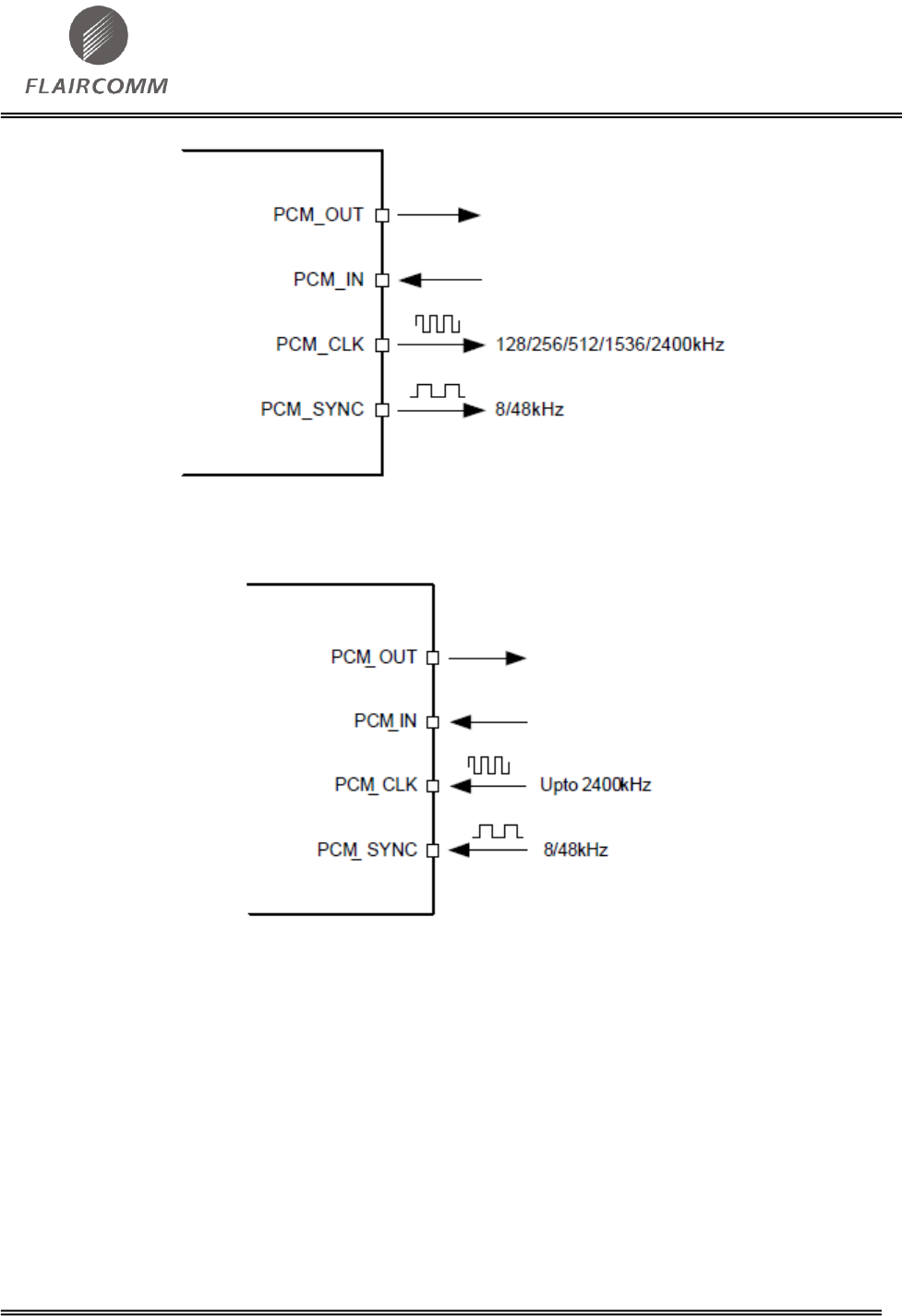
4.3.1 .1 PCM Interface Master/Slave
When configured as the master of the PCM interface, BTM805 generates PCM_CLK and
PCM_SYNC.
FLC-BTM805 Datasheet
Flaircomm Microelectronics Confidential
-16-
Figure 5: Configured PCM as a Master
Figure 6: Configured PCM as a Slave
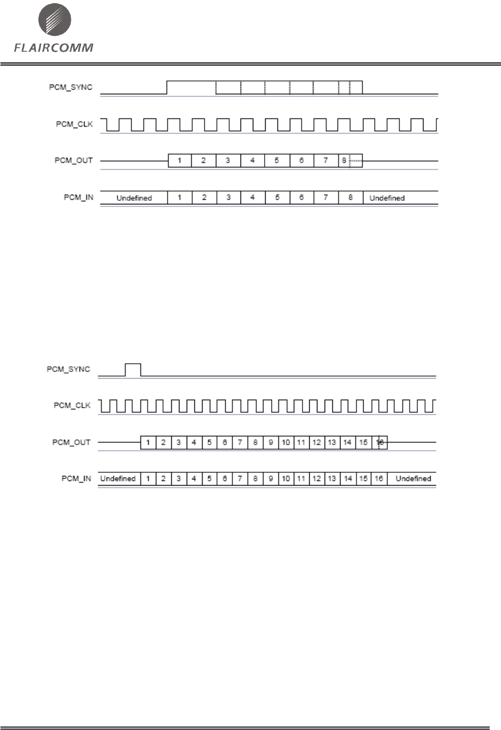
4.3.1.2 Long Frame Sync
Long Frame Sync is the name given to a clocking format that controls the transfer of PCM data
words or samples. In Long Frame Sync, the rising edge of PCM_SYNC indicates the start of the
PCM word. When BTM805 is configured as PCM master, generating PCM_SYNC and PCM_CLK,
then PCM_SYNC is 8-bits long. When BTM805 is configured as PCM Slave, PCM_SYNC is from
1 cycle PCM_CLK to half the PCM_SYNC rate.
FLC-BTM805 Datasheet
Flaircomm Microelectronics Confidential
-17-
Figure 7: Long Frame Sync (Shown with 8-bit Companded Sample)
BTM805 samples PCM_IN on the falling edge of PCM_CLK and transmits PCM_OUT on the rising
edge. PCM_OUT is configurable as high impedance on the falling edge of PCM_CLK in the LSB
position or on the rising edge.
4.3.1.3 Short Frame Sync
In Short Frame Sync, the falling edge of PCM_SYNC indicates the start of the PCM word.
PCM_SYNC is always one clock cycle long.
Figure 8: Short Frame Sync (Shown with 16-bit Sample)
As with Long Frame Sync, BTM805 samples PCM_IN on the falling edge of PCM_CLK and
transmits PCM_OUT on the rising edge. PCM_OUT may be configured to be high impedance on the
falling edge of PCM_CLK in the LSB position or on the rising edge.
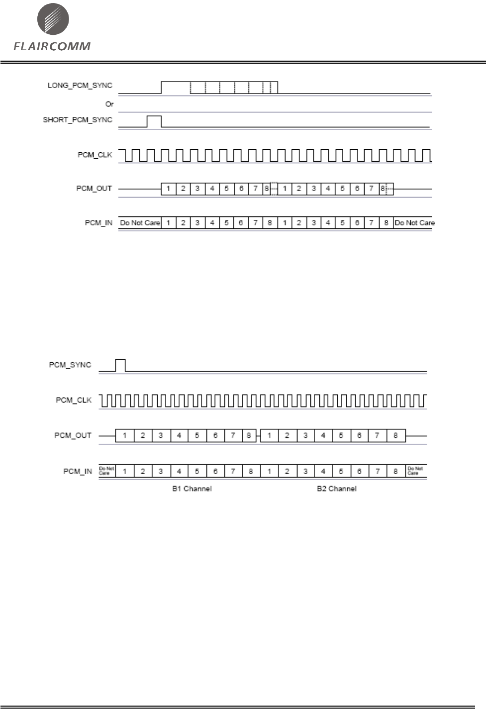
4.3.1.4 Multi-slot Operation
More than one SCO connection over the PCM interface is supported using multiple slots. Up to three
SCO connections can be carried over any of the first four slots.
FLC-BTM805 Datasheet
Flaircomm Microelectronics Confidential
-18-
Figure 9: Multi-Slot Operation with Two Slots and 8-bit Companded Samples
4.3.1.5 GCI Interface
BTM805 is compatible with the General Circuit Interface (GCI), a standard synchronous 2B+D
ISDN timing interface. The two 64Kbps B channels are accessed when this mode is configured.
Figure 10: GCI Interface
The start of a frame is indicated by the rising edge of PCM_SYNC and runs at 8kHz.
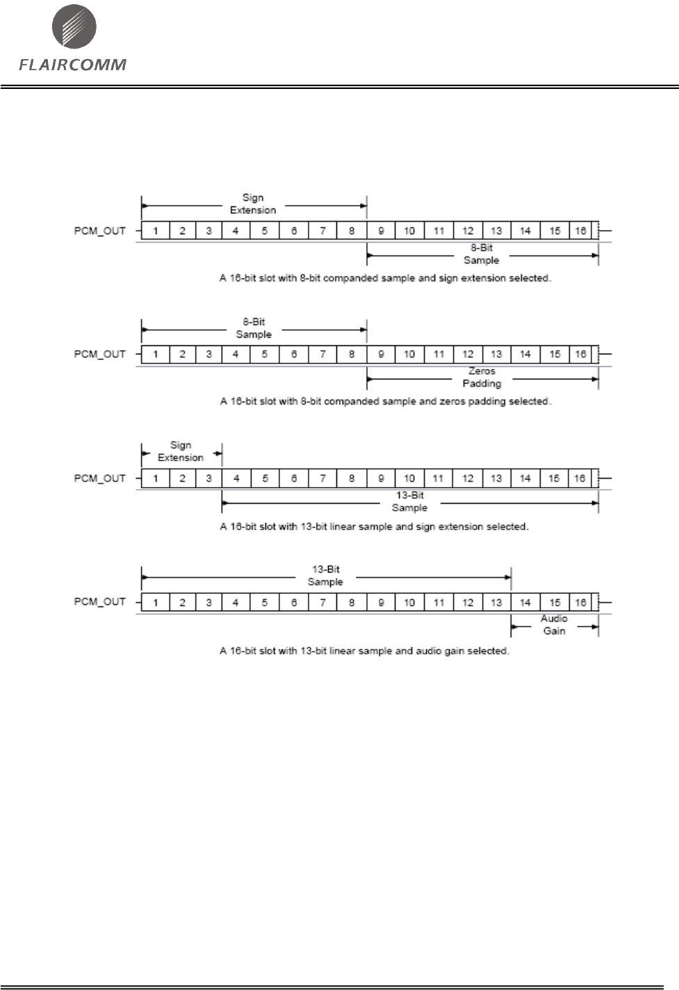
4.3.1.6 Slots and Sample Formats
BTM805receives and transmits on any selection of the first four slots following each sync pulse. Slot
durations are either 8 or 16 clock cycles.
8 clock cycles for 8-bit sample formats.
16 clock cycles for 8-bit, 13-bit or 16-bit sample formats.
BTM805 supports:
13-bit linear, 16-bit linear and 8-bit μ-law or A-law sample formats.
A sample rate of 8ksamples/s.
FLC-BTM805 Datasheet
Flaircomm Microelectronics Confidential
-19-
Little or big endian bit order.
For 16-bit slots, the 3 or 8 unused bits in each slot are filled with sign extension, padded with
zeros or a programmable 3-bit audio attenuation compatible with some codecs.
Figure 11: 16-Bit Slot Length and Sample Formats
4.3.1.7 Additional Features
BTM805 has a mute facility that forces PCM_OUT to be 0. In master mode, BTM805 is compatible
with some codecs which control power down by forcing PCM_SYNC to 0 while keeping
PCM_CLK running.
4.3.1.8 PCM Timing Information
FLC-BTM805 Datasheet
Flaircomm Microelectronics Confidential
-20-
Symbol
Parameter
Min
Typical
Max
Unit
fmclk
PCL_CLK
Frequency
4MHz DDS generation.
Selection of frequency
is programmable.
-
128
-
kHz
256
512
48MHz DDS
generation. Selection of
frequency is
programmable.
2.9
-
kHz
-
PCM_SYNC frequency for SCO
connection
-
8
kHz
tmclkh(a)
PCM_CLK
high
4MHz DDS generation
980
-
-
ns
tmclkl(a)
PCM_CLK low
4MHz DDS generation
730
-
ns
-
PCM_CLK
jitter
48MHz DDS
generation
21
ns pk-pk
Table 6: PCM Master Timing
(a) Assumes normal system clock operation. Figures vary during low-power modes, when system clock speeds are reduced.
Symbol
Parameter
Min
Typical
Max
Unit
tdmclksynch
Delay time from
PCM_CLK high
to PCM_SYNC
high
4MHz DDS generation
-
-
20
ns
48MHs DDS generation
-
-
40.83
ns
tdmclkpout
Delay time from PCM_CLK high to valid
PCM_OUT
-
-
20
ns
tdmclklsyncl
Delay time from
PCM_CLK low to
PCM_SYNC low
(Long Frame Sync
only)
4MHz DDS generation
-
-
20
ns
48MHz DDS
generation
-
-
40.83
ns
tdmclkhsyncl
Delay time from
PCM_CLK high
to PCM_SYNC
low
4MHz DDS generation
-
-
20
ns
48MHz DDS
generation
-
-
40.83
ns
tdmclklpoutz
Delay time from PCM_CLK low to
PCM_OUT high impedance
-
-
20
ns
tdmclkhpoutz
Delay time from PCM_CLK high to
PCM_OUT high impedance
-
-
20
ns
tsupinclkl
Set-up time for PCM_IN valid to PCM_CLK
low
20
-
-
ns
thpinclkl
Hold time for PCM_CLK low to PCM_IN
invalid
0
-
-
ns
Table 7: PCM Master Mode Timing Parameters
FLC-BTM805 Datasheet
Flaircomm Microelectronics Confidential
-21-
Figure 12: PCM Master Timing Long Frame Sync
Figure 13: PCM Master Timing Short Frame Sync
FLC-BTM805 Datasheet
Flaircomm Microelectronics Confidential
-22-
Symbol
Parameter
Min
Typical
Max
Unit
fsclk
PCM clock frequency (Slave mode: input)
64
-
2048
kHz
fsclk
PCM clock frequency (GCI mode)
128
-
4096
kHz
tsclkl
PCM_CLK low time
200
-
-
ns
tsclkh
PCM_CLK high time
200
-
-
ns
Table 8: PCM Slave Timing
thsclksynch
Hold time from PCM_CLK low to
PCM_SYNC high
2
-
-
ns
tsusclksynch
Set-up time for PCM_SYNC high to
PCM_CLK low
20
-
-
ns
tdpout
Delay time from PCM_SYNC or
PCM_CLK whichever is later, to valid
PCM_OUT data (Long Frame Sync only)
-
-
15
ns
tdsclkhpout
Delay time from CLK high to PCM_OUT
valid data
-
-
15
ns
tdpoutz
Delay time from PCM_SYNC or
PCM_CLK low, whichever is later, to
PCM_OUT data line high impedance
-
-
20
ns
tsupinsclkl
Set-up time for PCM_IN valid to CLK
low
20
-
-
ns
thpinsclkl
Hold time for PCM_CLK low to
PCM_IN invalid
2
-
-
ns
Table 9: PCM Slave Mode Timing Parameters
FLC-BTM805 Datasheet
Flaircomm Microelectronics Confidential
-23-
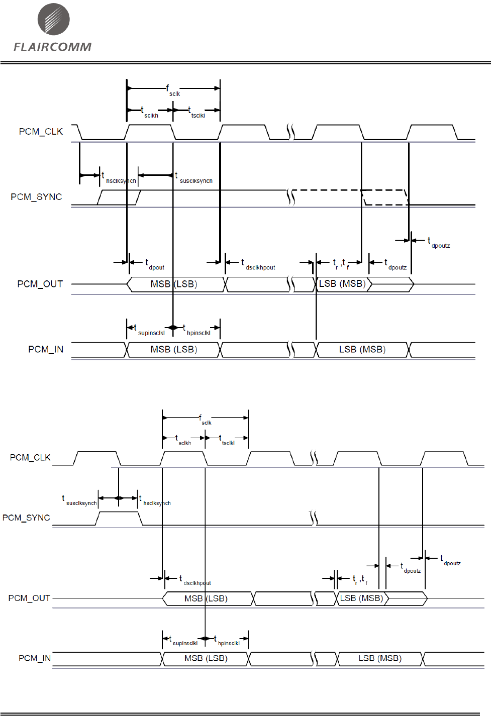
Figure 14: PCM Slave Timing Long Frame Sync
Figure 15: PCM Slave Timing Short Frame Sync
FLC-BTM805 Datasheet
Flaircomm Microelectronics Confidential
-24-
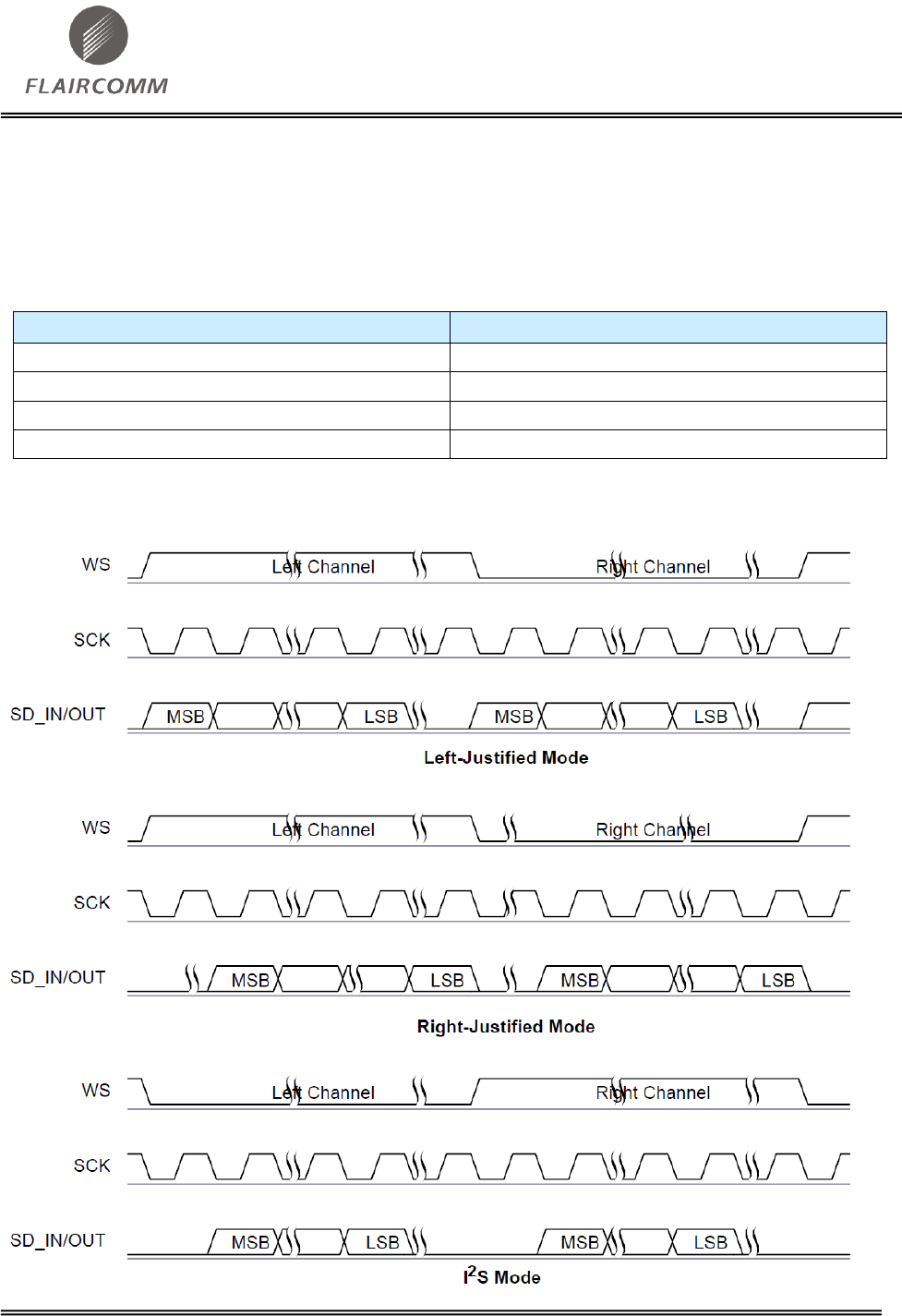
4.3.2 Digital Audio Interface (I2S)
The digital audio interface supports the industry standard formats for I2S, left-justified or right-
justified. The interface shares the same pins as the PCM interface, which means each audio bus is
mutually exclusive in its usage. Table 9 lists these alternative functions. Figure 14 shows the timing
diagram.
PCM Interface
I2S Interface
PCM_OUT
SD_OUT
PCM_IN
SD_IN
PCM_SYNC
WS
PCM_CLK
SCK
Table 10: Alternative Functions of the Digital Audio Bus Interface on the PCM Interface
Configure the digital audio interface using the PSKEY_DIGITAL-AUDIO-CONFIG, see your PS Key file.
FLC-BTM805 Datasheet
Flaircomm Microelectronics Confidential
-25-
Figure 16: Digital Audio Interface Modes
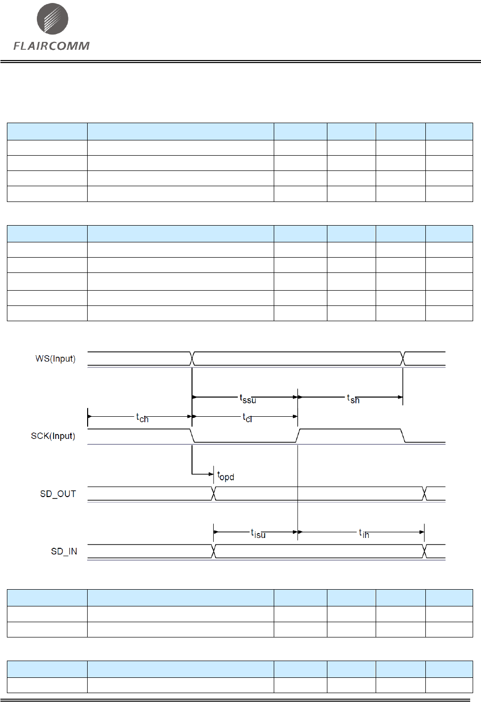
The internal representation of audio samples within BTM805 is 16-bit and data on SD_OUT is
limited to 16-bit per channel.
Symbol
Parameter
Min
Typical
Max
Unit
-
SCK Frequency
-
-
6.2
MHz
-
WS Frequency
-
-
96
kHz
Tch
SCK high time
80
-
-
ns
tcl
SCK low time
80
-
-
ns
Table 11: Digital Audio Interface Slave Timing
Symbol
Parameter
Min
Typical
Max
Unit
Tssu
WS valid to SCK high set-up time
20
-
-
ns
tsh
SCK high to WS invalid hold time
2.5
-
-
ns
Topd
SCK low to SD_OUT valid delay time
-
-
20
ns
tisu
SD_IN valid to SCK high set-up time
20
-
-
ns
Tih
SCK high to SD_IN invalid hold time
2.5
-
-
ns
Table 12: I2S Slave Mode Timing
Figure 17: Digital Audio Interface Slave Timing
Symbol
Parameter
Min
Typical
Max
Unit
-
SCK Frequency
-
-
6.2
MHz
-
WS Frequency
-
-
96
kHz
Table 13: Digital Audio Interface Slave Timing
Symbol
Parameter
Min
Typical
Max
Unit
Tspd
SCK low to WS valid delay time
-
-
39.27
ns
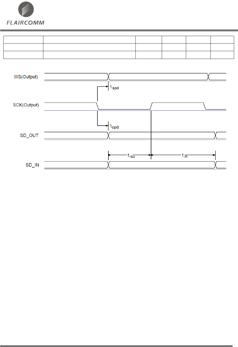
FLC-BTM805 Datasheet
Flaircomm Microelectronics Confidential
-26-
Topd
SCK low to SD_OUT valid delay time
-
-
18.44
ns
tisu
SD_IN valid to SCK high set-up time
18.44
-
-
ns
Tih
SCK high to SD_IN invalid hold time
0
-
-
ns
Table 14: Digital Audio Interface Slave Mode Timing Parameters
Figure 18: Digital Audio Interface Master Timing
4.4 RF Interface
The module integrates a balun filter. The user can connect a 50ohms antenna directly to the RF port
for BTM805CL2A. BTM805CL2B integrates an antenna internally.
4.5 General Purpose Digital IO
There are six general purpose digital IOs defined in the module. All these GPIOs can be configured
by software to realize various functions, such as button controls, LED displays or interrupt signals to
host controller, etc. Do not connect them if not use.
4.6 Host Interfaces
Use the host interface to:
Configure BTM805 to suit the target platform requirements
Transfer data to and from other Bluetooth devices.
BTM805 has a new automatic host transport selection scheme that does not require the use of PIOs.
4.6.1 UART Interface
This is a standard UART interface for communicating with other serial devices.
BTM805 UART interface provides a simple mechanism for communicating with other serial devices
using the RS232 protocol.
FLC-BTM805 Datasheet
Flaircomm Microelectronics Confidential
-27-
When BTM805 is connected to another digital device, UART_RX and UART_TX transfer data
between the two devices. The remaining 2 signals, UART_CTS and UART_RTS, implement RS232
hardware flow control where both are active low indicators.
If UART_CTS and UART_RTS are not required for hardware flow control, they are reconfigurable
as PIO.
UART configuration parameters, such as baud rate and packet format, are set using BTM805
firmware.
Note:
To communicate with the UART at its maximum data rate using a standard PC, an accelerated serial port
adapter card is required for the PC.
Parameter
Possible Values
Baud Rate
Minimum
1200 baud (≤2%Error)
9600 baud (≤1%Error)
Maximum
4M baud (≤1%Error)
Flow control
RTS/CTS or None
Parity
None, Odd or Even
Number of Stop Bits
1 or 2
Bits per Byte
8
Table 15: Possible UART Settings
4.6.2 UART Configuration While Reset is Active
The UART interface for BTM805 is a tri-state while the chip is being held in reset. This enables the
user to daisy chain devices onto the physical UART bus. This constraint on this method is that any
devices connected to this bus must tri-state when BTM805 reset is de-asserted and the firmware
begins to run.
FLC-BTM805 Datasheet
Flaircomm Microelectronics Confidential
-28-
5. Electrical Characteristic
5.1 Absolute Maximum Ratings
Ratings
Min
Max
Unit
Storage Temperature
-40
+85
°C
VBAT operation(a)
2.3
4.8
V
Low-voltage operation (bypassing high-voltage linear regulator)
1.7
2.0
V
I/O supply voltage
-0.4
+3.6
V
Other Terminal Voltages
VSS-0.4
VDD+0.4
V
Table 16: Absolute Maximum Rating
5.2 Recommended Operating Conditions
Operating Condition
Min
Max
Unit
Operating Temperature Range
for A and I grade
-40
+85
°C
for V and C grade
-20
+70
°C
VBAT operation
2.3
4.8
V
Low-voltage operation (bypassing high-voltage linear regulator)
+1.75
+1.95
V
I/O supply voltage ( VDD_PADS)
+1.2
+3.6
V
Table 17: Recommended Operating Conditions
5.3 Input/output Terminal Characteristics
5.3.1 High-voltage Linear Regulator
Normal Operation
Min
Typical
Max
Unit
Input voltage
2.3
3.3
4.8
V
Output voltage
1.75
1.85
1.95
V
Temperature coefficient
-200
-
200
ppm/°C
Output noise (frequency range 100Hz to 100kHz)
-
-
0.4
mV rms
Setting time (setting to within 10% of final value)
-
-
5
μs
Output current
-
-
100
mA
Quiescent current(excluding load, < )
30
40
60
μA
Low-power Modes
Quiescent current(excluding load, < )
14
18
23
μA
FLC-BTM805 Datasheet
Flaircomm Microelectronics Confidential
-29-
5.3.2 Low-voltage VDD_DIG linear Regulator
Normal Operation
Min
Typical
Max
Unit
Output voltage
0.90
-
1.25
V
Output current
-
-
30
mA
5.3.3 Low-voltage VDD_AUX Linear Regulator
Normal Operation
Min
Typical
Max
Unit
Output voltage
1.30
1.35
1.40
V
Output current
-
-
5
mA
5.3.4 Low-voltage VDD_RADIO Linear Regulator
Normal Operation
Min
Typical
Max
Unit
Output voltage
1.30
1.35
1.45
V
Output current
-
-
60
mA
5.3.5 Digital
Digital Terminals
Min
Typical
Max
Unit
Input Voltage Levels
VIL input logic level low
-0.4
-
+0.4
V
VIH input logic level high
0.7×VDD
-
VDD+0.4
V
Output Voltage Levels
VOL output logic level low, lOL = 4.0mA
-
-
0.4
V
VOH output logic level high, lOH = -4.0mA
0.75×VDD
-
-
V
Input and Tri-state Current
Strong pull-up
-150
-40
-10
μA
Strong pull-down
10
40
150
μA
Weak pull-up
-5
-1.0
`-0.33
μA
Weak pull-down
0.33
1.0
5.0
μA
input capacitance
1.0
-
5.0
pF
FLC-BTM805 Datasheet
Flaircomm Microelectronics Confidential
-30-
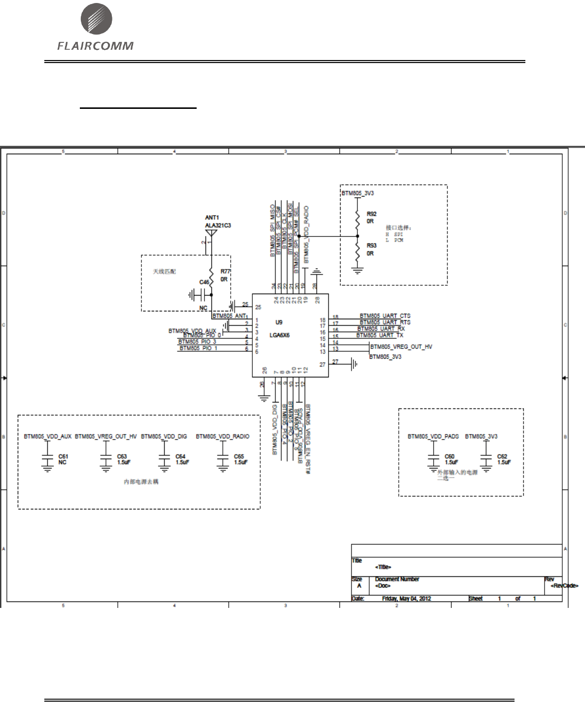
6. Reference Design
Figure 19: Reference Design
FLC-BTM805 Datasheet
Flaircomm Microelectronics Confidential
-31-
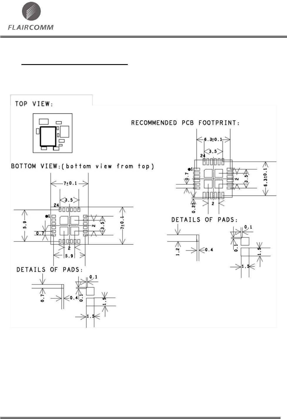
7. Mechanical Characteristic
BTM805CL2A (without Antenna):
Figure 20: BTM805CL2A Footprint
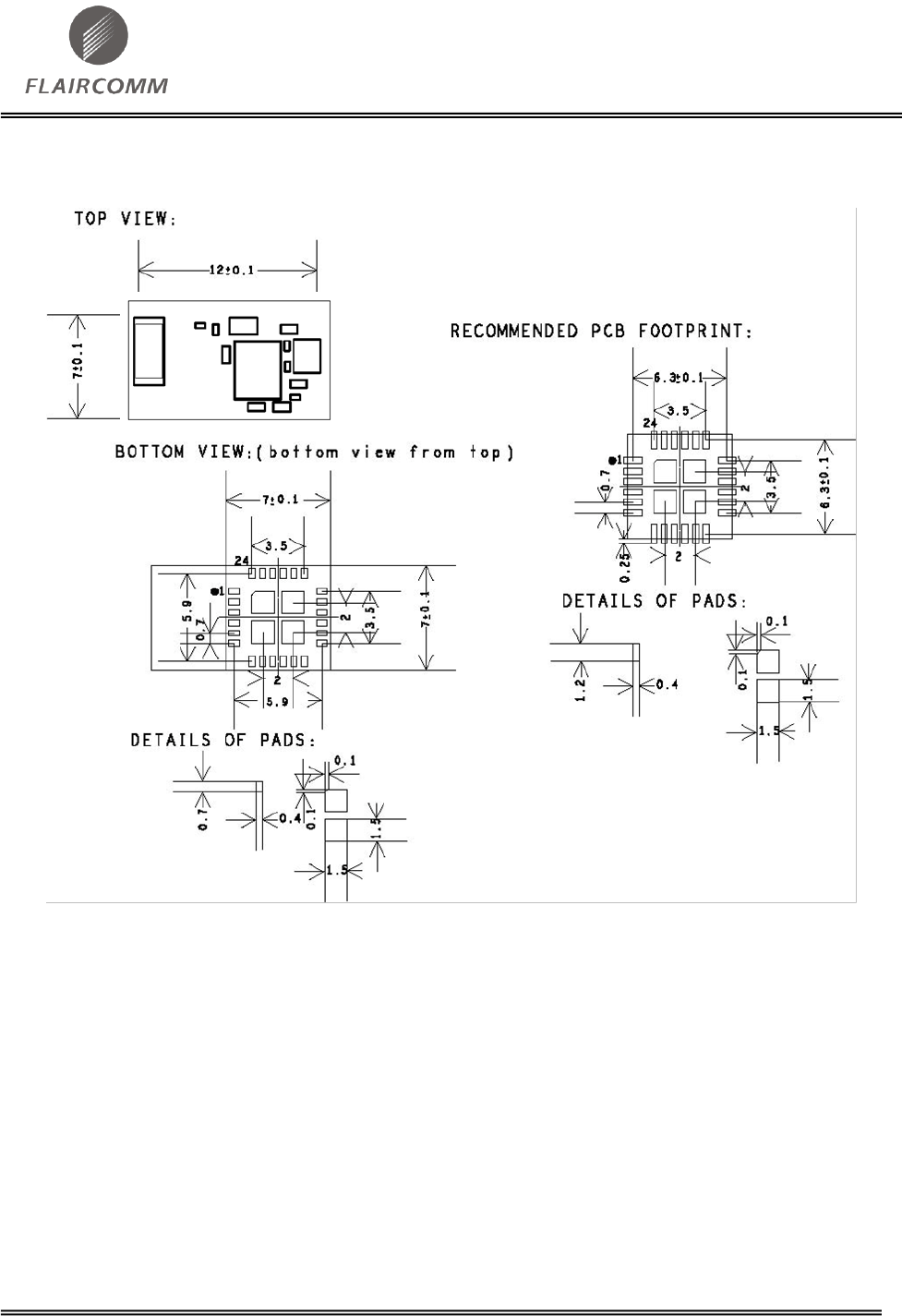
FLC-BTM805 Datasheet
Flaircomm Microelectronics Confidential
-32-
BTM805CL2B (with Antenna):
Figure 21: BTM805CL2B Footprint
FLC-BTM805 Datasheet
Flaircomm Microelectronics Confidential
-33-
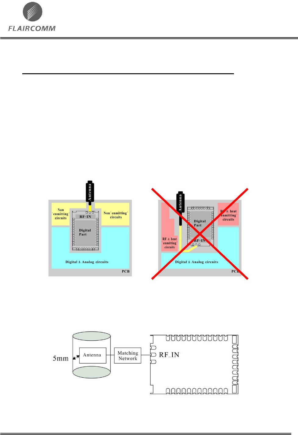
8. Recommended PCB Layout and Mounting Pattern
Placement and PCB layout are critical to optimize the performances of a module without on-board
antenna designs. The trace from the antenna port of the module to an external antenna should be 50
and must be as short as possible to avoid any interference into the transceiver of the module. The
location of the external antenna and RF-IN port of the module should be kept away from any noise
sources and digital traces. A matching network might be needed in between the external antenna and
RF-IN port to better match the impedance to minimize the return loss.
As indicated in Figure 22 below, RF critical circuits of the module should be clearly separated from
any digital circuits on the system board. All RF circuits in the module are close to the antenna port.
The module, then, should be placed in this way that module digital part towards your digital section
of the system PCB.
Figure 22: Placement the Module on a System Board
8.1 Antenna Connection and Grounding Plane Design
Figure 23: Leave 5mm Clearance Space from the Antenna
General design recommendations are:
The length of the trace or connection line should be kept as short as possible.
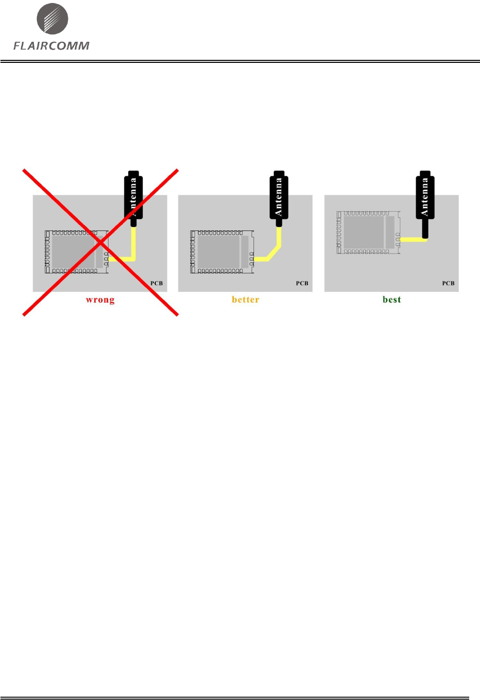
FLC-BTM805 Datasheet
Flaircomm Microelectronics Confidential
-34-
Distance between connection and ground area on the top layer should at least be as large as the
dielectric thickness.
Routing the RF close to digital sections of the system board should be avoided.
To reduce signal reflections, sharp angles in the routing of the micro strip line should be avoided.
Chamfers or fillets are preferred for rectangular routing; 45-degree routing is preferred over
Manhattan style 90-degree routing.
Figure 24: Recommended Trace Connects Antenna and the Module
Routing of the RF-connection underneath the module should be avoided. The distance of the
micro strip line to the ground plane on the bottom side of the receiver is very small and has huge
tolerances. Therefore, the impedance of this part of the trace cannot be controlled.
Use as many vias as possible to connect the ground planes.
FLC-BTM805 Datasheet
Flaircomm Microelectronics Confidential
-35-
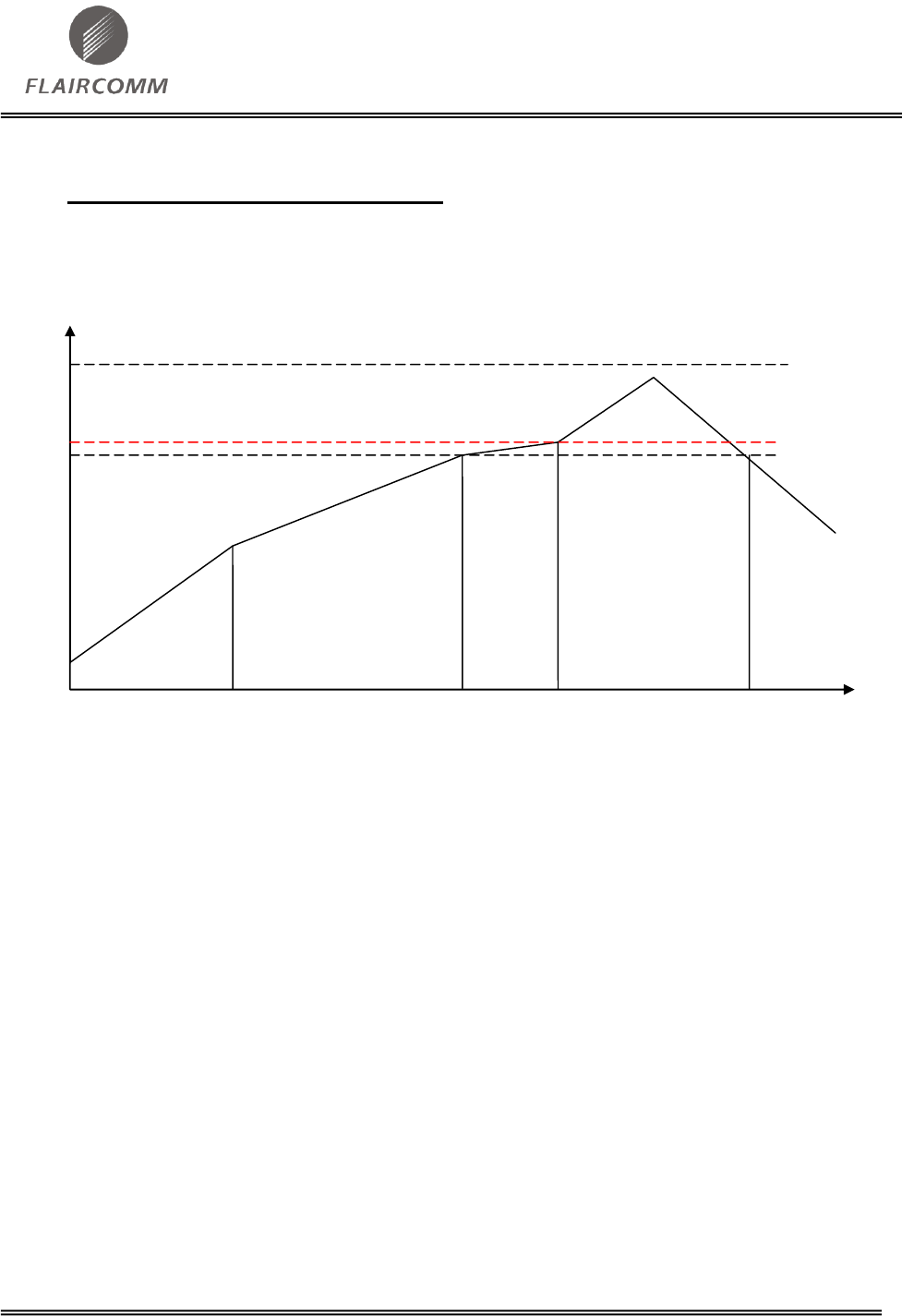
9. Recommended Reflow Profile
The soldering profile depends on various parameters necessitating a set up for each application. The
data here is given only for guidance on solder reflow.
210
217
℃
250
A
B
C
D
1
2
0
25
3
4
5
6
min
E
Figure 25: Recommended Reflow Profile
Pre-heat zone (A) — This zone raises the temperature at a controlled rate, typically 0.5 – 2 C/s.
The purpose of this zone is to preheat the PCB board and components to 120 ~ 150 C. This stage is
required to distribute the heat uniformly to the PCB board and completely remove solvent to reduce
the heat shock to components.
Equilibrium Zone 1 (B) — In this stage the flux becomes soft and uniformly encapsulates solder
particles and spread over PCB board, preventing them from being re-oxidized. Also with elevation
of temperature and liquefaction of flux, each activator and rosin get activated and start eliminating
oxide film formed on the surface of each solder particle and PCB board. The temperature is
recommended to be 150 to 210 for 60 to 120 second for this zone.
Equilibrium Zone 2 (c) (optional) — In order to resolve the upright component issue, it is
recommended to keep the temperature in 210 – 217 for about 20 to 30 second.
Reflow Zone (D) — The profile in the figure is designed for Sn/Ag3.0/Cu0.5. It can be a reference
for other lead-free solder. The peak temperature should be high enough to achieve good wetting but
not so high as to cause component discoloration or damage. Excessive soldering time can lead to
intermetallic growth which can result in a brittle joint. The recommended peak temperature (Tp) is
230 ~ 250 C. The soldering time should be 30 to 90 second when the temperature is above 217 C.
Cooling Zone (E) — The cooling ate should be fast, to keep the solder grains small which will give
a longerlasting joint. Typical cooling rate should be 4 C.
FLC-BTM805 Datasheet
Flaircomm Microelectronics Confidential
-36-
10. Ordering Information
10.1 Product Packaging Information
TBD
Figure 26: Product Packaging Information
10.2 Ordering information
FLC-BTM805XYZA
Product Revision
Shipping Package
Product Package
Product Grade
Figure 27: Ordering Information
Host Interface
Package
Order Number
Type
Shipment
BTM805CL2A
BTM805CL2B
UART
LGA
Tape and reel
10.2.1 Product Revision
Product Revision
Description
Availability
A
Without internal antenna
Yes
B
With an internal antenna
Yes
Table 18: Product Revision
10.2.2 Shipping Package
Shipping Package
Description
Quantity
Availability
0
Foam Tray
—
No
1
Plastic Tray
100x10x3 = 3000
Yes
2
Tape
—
Yes
Table 19: Shipping Package
FLC-BTM805 Datasheet
Flaircomm Microelectronics Confidential
-37-
10.2.3 Product Package
Product Package
Description
Availability
Q
QFN
No
L
LGA
Yes
B
BGA
No
C
Connector
No
Table 20: Product Package
10.2.4 Product Grade
Product Grade
Description
Availability
C
Consumer
Yes
I
Industrial
Yes
V
Automobile After-Market
Yes
A
Automobile Before-Market
No
Table 21: Product Grade

FLC-BTM805 Datasheet
Flaircomm Microelectronics Confidential
-38-
11. Cautions &Warnings
11.1 FCC Statement
1. This device complies with Part 15 of the FCC Rules. Operation is subject to the following two
conditions:
(1) This device may not cause harmful interference.
(2) This device must accept any interference received, including interference that may cause
undesired operation.
2. Changes or modifications not expressly approved by the party responsible for compliance could
void the user's authority to operate the equipment.
NOTE: This equipment has been tested and found to comply with the limits for a Class B digital
device, pursuant to Part 15 of the FCC Rules. These limits are designed to provide reasonable
protection against harmful interference in a residential installation.
This equipment generates uses and can radiate radio frequency energy and, if not installed and used
in accordance with the instructions, may cause harmful interference to radio communications.
However, there is no guarantee that interference will not occur in a particular installation. If this
equipment does cause harmful interference to radio or television reception, which can be determined
by turning the equipment off and on, the user is encouraged to try to correct the interference by one
or more of the following measures:
Reorient or relocate the receiving antenna.
Increase the separation between the equipment and receiver.
Connect the equipment into an outlet on a circuit different from that to which the receiver is
connected.
Consult the dealer or an experienced radio/TV technician for help.
This radio module must not be installed to co-locate and operate simultaneously with other radios in
host system; additional testing and equipment authorization may be required to operating
simultaneously with other radios.
11.2 RF Warning Statement
The device has been evaluated to meet general RF exposure requirement. The device can be used in
portable exposure condition without restriction.
11.3 FLC-BTM805 Label Instructions
The FLC-BTM805 module is designed to comply with the FCC statements.
FLC-BTM805 Datasheet
Flaircomm Microelectronics Confidential
-39-
The packaging of host system that uses BTM805 should display a label indicating the information as
follows:
Contains FCC ID: P4IBTM805
Model: FLC-BTM805
(Series models: FLC-BTM805IL2A/ FLC-BTM805CL2A/ FLC-BTM805VL2A/
FLC-BTM805IL2B/ FLC-BTM805CL2B/ FLC-BTM805VL2B)
Any similar wording that expresses the same meaning may also be used.
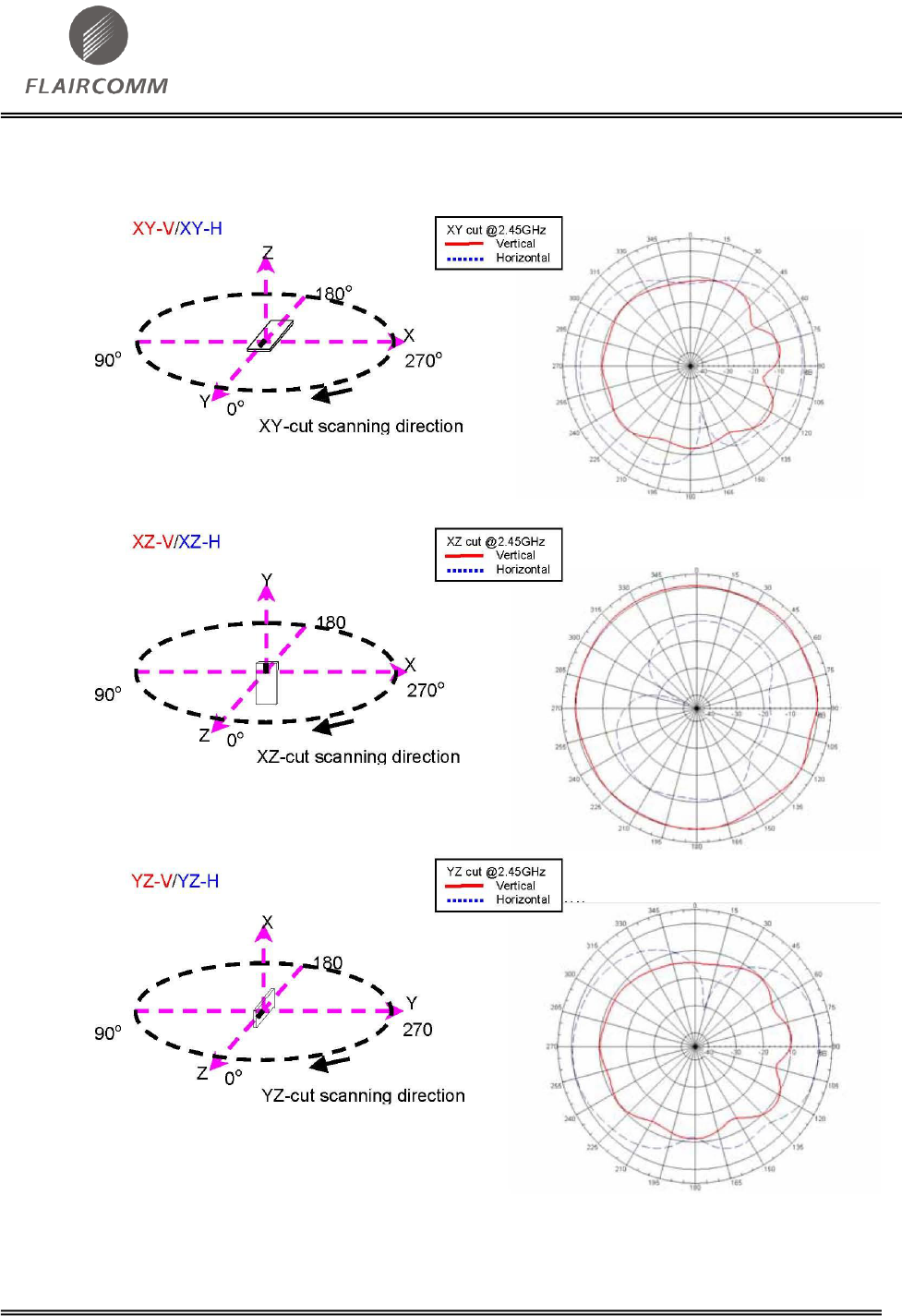
11.4 FLC-BTM805 Antenna Statement
Note: In this section, “A” and “B” in “BTM805A” and “BTM805B” refer to Product Revision.
Please see Section 10.2.1 for reference.
11.4.1 BTM805A (Without Antenna)
There is no built-in antenna in BTM805A. BTM805A is integrated with a UFL connector to make it
simple for designers to add an external antenna into the module. In order to make the product
compliant with the FCC standard, the applicable antennas which designers choose should be similar
to the antenna in BTM805B in specifications and radiation patterns. And the gain should be less than
the peak gain of the antenna in BTM805B. If designers choose a different antenna, additional testing
and equipment authorization are needed to ensure the compliance with FCC statement.
11.4.2 BTM805B (With Antenna)
Antenna specifications of BTM805B are listed in the following table:
Part Number
Frequency Range
(MHz)
Peak Gain
(XZ-V)
Average Gain
(XZ-V)
VSWR
Impedance
AT3216-
B2R7HAA_
2400 ~ 2500
0.5 dBi typ.
-0.5 dBi typ.
2 max.
50 Ω
Table 22: Antenna Specifications
Operating Temperature Range:-40 ~ +85 oC
Storage Temperature Range: -40 ~ +85 oC
Power Capacity: 3W max.
FLC-BTM805 Datasheet
Flaircomm Microelectronics Confidential
-40-
The following figures show the Radiation Patterns of the antenna in BTM805B.
Figure 28: Radiation Patterns of Antenna