Flaircomm Microelectronics CBM202 WiFi and BT combo module User Manual FLC BTM401 DS
Fujian Flaircomm Microelectronics,Inc. WiFi and BT combo module FLC BTM401 DS
User Manual
FLC-CBM202 Datasheet
Flaircomm Microelectronics Confidential
-1-
FLC-CBM202
Datasheet
Document Type: Combo Module Datasheet
Document Number: FLC-CBM202-DS
Document Version: V1.2
Release Date: Feb.22, 2013
Copyright 2012 ~ 2014 by Flaircomm Microelectronics, Inc., All Right Reserved
Without written permission from Flaircomm Microelectronics, Inc., reproduction, transfer, distribution or
storage of part or all of the contents in this document in any form is prohibited
FLC-CBM202 Datasheet
Flaircomm Microelectronics Confidential
-2-
Release Record
Version
Release Date
Comments
0.1
June 16, 2011
Preliminary Release
0.2
August 05, 2011
Add Section5.2
1.0
July 3, 2012
1.1
Jan. 11, 2013
Add Section 11
1.2
Feb.22,2013
Modify Frequency Band.

FLC-CBM202 Datasheet
Flaircomm Microelectronics Confidential
-3-
CONTENTS
1. INTRODUCTION .................................................................................................................................................. 6
1.1 BLOCK DIAGRAM .................................................................................................................................................. 6
1.2 FEATURES ............................................................................................................................................................. 6
1.2.1 WiFi Features ............................................................................................................................................... 6
1.2.2 Bluetooth Features ........................................................................................................................................ 7
1.3 FUNCTIONS ........................................................................................................................................................... 7
1.3.1 WiFi Functions ............................................................................................................................................. 7
1.3.2 Bluetooth Functions ..................................................................................................................................... 8
1.4 APPLICATIONS ...................................................................................................................................................... 9
2. GENERAL SPECIFICATION ........................................................................................................................... 10
3. PIN DEFINITION ................................................................................................................................................ 12
3.1 PIN CONFIGURATION ........................................................................................................................................... 12
3.2 PIN DEFINITION ................................................................................................................................................... 12
4. PHYSICAL INTERFACES ................................................................................................................................ 15
4.1 WIFI POWER SUPPLY .......................................................................................................................................... 15
4.1.1 Linear Regulator for Digital Supply ........................................................................................................... 15
4.1.2 Linear Regulator for Analogue Supply ...................................................................................................... 15
4.1.3 RF Front End Power Supply ...................................................................................................................... 15
4.1.4 I/O Power Supply ....................................................................................................................................... 15
4.2 BT POWER SUPPLY ............................................................................................................................................. 15
4.3 RESET ................................................................................................................................................................. 15
4.3.1 WiFi reset ................................................................................................................................................... 16
4.3.2 BT Reset ..................................................................................................................................................... 16
4.4 RF INTERFACE .................................................................................................................................................... 16
4.5 HOST INTERFACE ................................................................................................................................................ 17
4.5.1 WiFi Host Interfaces .................................................................................................................................. 17
4.5.2 Bluetooth UART Host Interfaces ............................................................................................................... 19
4.6 AUDIO INTERFACE .............................................................................................................................................. 19
4.6.1 PCM Interface ............................................................................................................................................ 19
4.6.2 Digital Audio Interface (I²S) ...................................................................................................................... 21
5. ELECTRICAL CHARACTERISTIC ................................................................................................................ 22
5.1 WIFI PERFORMANCE SPECIFICATIONS ................................................................................................................ 22
5.1.1 DSSS and CCK modulations (802.11b) TX Performance Specifications .................................................. 22
5.1.2 OFDM TX Performance Specifications ..................................................................................................... 22
5.1.3 DSSS and CCK modulations (802.11b) RX Performance Specifications .................................................. 23
5.1.4 OFDM RX Performance Specifications ..................................................................................................... 23
5.2 BLUETOOTH PERFORMANCE SPECIFICATIONS ..................................................................................................... 25
5.2.1 Transmitter ................................................................................................................................................. 25
5.2.2 Receiver ...................................................................................................................................................... 26
5.3 DC ELECTRICAL SPECIFICATIONS ....................................................................................................................... 27
5.3.1 Absolute Maximum Ratings ....................................................................................................................... 27
5.3.2 Recommended Operating Conditions ......................................................................................................... 27
5.3.3 Current Consumption ................................................................................................................................. 27
5.3.4 Digital Characteristics ................................................................................................................................ 28
5.3.5 Sleep Clock Characteristics ........................................................................................................................ 28
5.3.6 Power-on Reset Characteristics .................................................................................................................. 29
6. REFERENCE DESIGN ....................................................................................................................................... 30
7. MECHANICAL CHARACTERISTIC .............................................................................................................. 31
8. RECOMMENDED PCB LAYOUT AND MOUNTING PATTERN............................................................... 32

FLC-CBM202 Datasheet
Flaircomm Microelectronics Confidential
-4-
8.1 ANTENNA CONNECTION AND GROUNDING PLANE DESIGN ................................................................................. 32
9. RECOMMENDED REFLOW PROFILE ......................................................................................................... 34
10. ORDERING INFORMATION ....................................................................................................................... 35
10.1 PRODUCT PACKAGING INFORMATION ................................................................................................................. 35
10.2 ORDERING INFORMATION .................................................................................................................................... 35
10.2.1 Product Revision ........................................................................................................................................ 35
10.2.2 Shipping Package ....................................................................................................................................... 35
10.2.3 Product Package ......................................................................................................................................... 35
10.2.4 Product Grade ............................................................................................................................................. 36
11. CAUTIONS &WARNINGS ............................................................................................................................ 37
11.1 FCC STATEMENT ................................................................................................................................................ 37
11.2 FCC RADIATION EXPOSURE STATEMENT ........................................................................................................... 37
11.3 FLC-CBM202 LABEL INSTRUCTIONS ................................................................................................................. 37
11.4 FLC-CBM202 ANTENNA STATEMENT ............................................................................................................... 38
11.4.1 Antenna Electrical Specifications............................................................................................................... 38
11.4.2 Radiation Gain and Pattern ......................................................................................................................... 38

FLC-CBM202 Datasheet
Flaircomm Microelectronics Confidential
-5-
TABLES AND FIGURES
Table 1: General Specification ....................................................................................................................................... 11
Table 2: Pin Definition ................................................................................................................................................... 14
Table 3: Analog IO Usage .............................................................................................................................................. 17
Table 4: PCM and I2S Digital Audio Interface .............................................................................................................. 21
Table 5: DSSS and CCK modulations (802.11b) TX Performance Specifications ........................................................ 22
Table 6: OFDM TX Performance Specifications ........................................................................................................... 23
Table 7: DSSS and CCK modulations (802.11b) RX Performance Specifications ........................................................ 23
Table 8: OFDM RX Performance Specifications ........................................................................................................... 25
Table 9: Transmitter ....................................................................................................................................................... 26
Table 10: Receiver ......................................................................................................................................................... 26
Table 11: Absolute Maximum Ratings .......................................................................................................................... 27
Table 12: Recommended Operating Conditions ............................................................................................................ 27
Table 13: WiFi Current Consumption ............................................................................................................................ 27
Table 14: BT Current Consumption ............................................................................................................................... 28
Table 15: Digital Characteristics .................................................................................................................................... 28
Table 16: Sleep Clock Characteristics ............................................................................................................................ 28
Table 17: Power-on Reset Characteristics ...................................................................................................................... 29
Table 18: Product Revision ............................................................................................................................................ 35
Table 19: Shipping Package ........................................................................................................................................... 35
Table 20: Product Package ............................................................................................................................................. 35
Table 21: Product Grade ................................................................................................................................................ 36
Table 20: Antenna Electrical Specifications .................................................................................................................. 38
Table 21: Radiation Gain and Pattern ............................................................................................................................ 38
Figure 1: Block Diagram .................................................................................................................................................. 6
Figure 2: Pin Configuration............................................................................................................................................ 12
Figure 3: UART_TX Timing ......................................................................................................................................... 19
Figure 4: PCM Interface Master ..................................................................................................................................... 20
Figure 5: PCM Interface Slave ....................................................................................................................................... 20
Figure 6: Reference Design ............................................................................................................................................ 30
Figure 7: Module Size (Top View and Side View) ........................................................................................................ 31
Figure 8: Footprint (Top View) ...................................................................................................................................... 31
Figure 9: Pin dimensions ................................................................................................................................................ 31
Figure 10: Placement the Module on a System Board ................................................................................................... 32
Figure 11: Leave 5mm Clearance Space from the Antenna ........................................................................................... 32
Figure 12: Recommended Trace Connects Antenna and the Module ............................................................................ 33
Figure 13: Recommended Reflow Profile ...................................................................................................................... 34
Figure 14: Product Packaging Information .................................................................................................................... 35
Figure 15: Ordering Information .................................................................................................................................... 35
Figure 12: ALA931C5 Radiation Pattern : Azimuth@2.45GHz .................................................................................... 39
Figure 13: ALA931C5 Radiation Pattern : Elevation1@2.45GHz ............................................................................... 40
Figure 14: ALA931C5 Radiation Pattern : Elevation2@2.45GHz ............................................................................... 41
FLC-CBM202 Datasheet
Flaircomm Microelectronics Confidential
-6-
1. Introduction
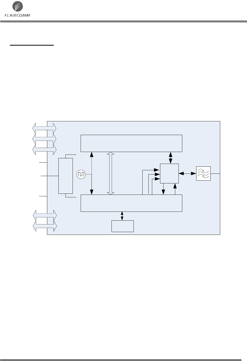
FLC-CBM202 is a highly integrated module that combines WiFi and BT in a small single package.
The module supports SDIO and CSPI host interfaces for WiFi and UART for BT that make it simple
to design into fully certified embedded WiFi and BT solutions.
The module is an appropriate product for designers who want to add wireless capability to their
products.
1.1 Block Diagram
FEM
CSR6030/1
26 MHz
Power Supply
BPF
Antenna
SDIO
CSPI
TX
RX
FEM control
VDD_SDIO
VREG_IN_ANA
VREG_IN_DIG
VDD_RF
BT Reset
EEPROM
CSR8810/1
BT
WiFi Reset
UART
PCM
Audio
BT
WiFi
WiFi+BT
Coexistence
Figure 1: Block Diagram
1.2 Features
1.2.1 WiFi Features
Low cost, low power, highly integrated IEEE 802.11b/g/n,
Support Independent Basic Service Set (IBSS), e.g. ad hoc, BSS and Extended Service Set (ESS)
network configurations.
IEEE 802.11n support, including MPDU and MSDU aggregation, immediate block
acknowledgement, PSMP and STBC for improved rate, range and performance.
Intelligent power control, including IEEE802.11 power saving mode.
SDIO (4-bit and 1-bit) and CSPI will be employed to interface with host device (Android, Linux
and WinCE).
Support open system and shared key authentication services.

FLC-CBM202 Datasheet
Flaircomm Microelectronics Confidential
-7-
Internal WEP engine allows 64 or 128 bit Encryption with Temporal Key Integrity Protocol
(TKIP)
Hardware encryption support for WEP40/64, WEP 104/128, TKIP, CCMP (AES), BIP and
CKIP provides functionality for WPA, WPA2, IEEE802.11i, 802.11w and CCX advanced
security mechanisms. Module support WAPI security in China also.
Support 802.11e Quality of Service (QoS) with WMM Power Save ensures that mobile
solutions can achieve optimal battery life.
Advanced WiFi and BT coexistence schemes provide exceptional performance for WiFi and BT
using a single antenna.
RoHS Compliant
Support WiFi direct and soft AP function.
1.2.2 Bluetooth Features
Fully qualified BT 3.0 system
Support BT 4.0 (low energy)
Compliant to BT 3.0 + HS system
Class 1 and Class 2 BT power levels
High-sensitivity BT receiver
Fully-speed BT operation with full piconet and scatternet support
High-speed UART port (up to 4Mbps)
PCM/I2S digital audio interface
1.3 Functions
1.3.1 WiFi Functions
Transmitter
Receiver
Single antenna BT coexistence
Modulations
IEE802.11b modulations;
1Mbps / 2Mbps / 5.5Mbps / 11Mbps
IEEE802.11g OFDM;
6Mbps / 9Mbps / 12Mbps / 18Mbps / 24Mbps / 36Mbps / 48Mbps / 54Mbps
IEEE802.11n HT modulations MCS0-7, 20MHz, 800 and 400 ns guard interval;
6.5Mbps / 7.2Mbps / 13Mbps / 14.4Mbps / 19.5Mbps / 21.7Mbps / 26.0Mbps /
28.9Mbps / 39.0Mbps / 43.3Mbps / 52.0Mbps / 57.8Mbps / 58.5Mbps / 65.0Mbps /
72.2Mbps

FLC-CBM202 Datasheet
Flaircomm Microelectronics Confidential
-8-
MAC
Comprehensive MAC functionality according to IEEE 802.11-2007, including QoS traffic
scheduling;
Support the following optional IEEE802.11n features;
MPDU aggregation
MSDU aggregation
Immediate Block Acknowledgement
PSMP
MTBA
RIFS
L-SIG TXOP protection
Link adaptation using MCS feedback
Encryption
Hardware encryption according to IEEE 802.11-2007 and IEEE802.11w-2009;
WEP40/64
WEP104/128
CCMP(AES)
TKIP
BIP
Hardware encryption support for SMS4 to support WAPI (China)
Hardware encryption support Cisco CKIP
1.3.2 Bluetooth Functions
Transmitter
Class 1, Class 2 and Class 3 support without need for external power amplifier or TX/RX
switch
DQPSK and 8DPSK
Receiver
Integrated channel filters
Digital demodulator for improved sensitivity and co-channel rejection
Real time digitized RSSI available on HCI interface
DQPSK and 8DPSK
Support BT3.0
Support BT4.0

FLC-CBM202 Datasheet
Flaircomm Microelectronics Confidential
-9-
Physical Interfaces
UART
BCSP, H4, H4DS and H5 support
PCM/I2S interface
Synchronous serial interface up to 4Mbps for system debugging
1.4 Applications
Cellular phones
Tablet PCs
Handheld devices
Industrial applications
FLC-CBM202 Datasheet
Flaircomm Microelectronics Confidential
-10-
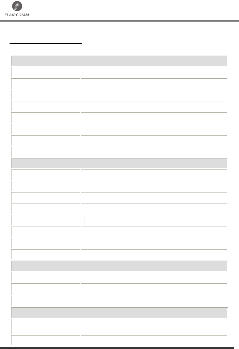
2. General Specification
WiFi Specification
Standard
IEEE 802.11b/g/n
Frequency Range
FCC : 2.412GHz-2.462GHz CE :2.422GHz -2.472GHz
Maximum Data Rate
72.2Mbps
RF Input Impedance
50 ohms
Interface
SDIO / SPI
Sensitivity
Refer to 5.1
RF TX Power
Refer to 5.1
Encryption
WEP40/64/104/128, CCMP(AES), TKIP, BIP, WAPI
Bluetooth Specification
Standard
BT 3.0 / BT 4.0
Frequency Band
2.402GHz ~ 2.480GHz
Maximum Data Rate
4Mbps
RF Input Impedance
50 ohms
Host Interface
UART
Audio Interface
PCM/I2S
Sensitivity
-87dBm
RF TX Power
6dBm (class 1.5)
Power
Supply Voltage
1.8 and 3.3V DC
Working Current
Refer to 5.3.3
Standby Current
Refer to 5.3.3
Operating Environment
Temperature
-40ºC to +85ºC for A and I grade
-20ºC to +70ºC for V and C grade
Humidity
10%~90% Non-Condensing

FLC-CBM202 Datasheet
Flaircomm Microelectronics Confidential
-11-
Certifications
WiFi Alliance/FCC/CE
Environmental
RoHS Compliant
Dimension and Weight
Dimension
9.9mm x 9.9mm x1.4mm
Weight
TBD
Table 1: General Specification
FLC-CBM202 Datasheet
Flaircomm Microelectronics Confidential
-12-
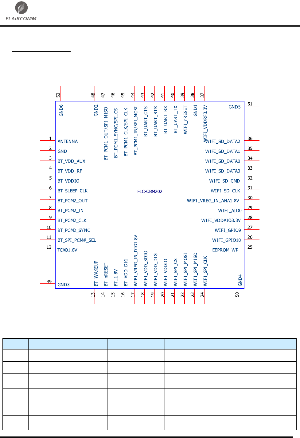
3. Pin Definition
3.1 Pin Configuration
Figure 2: Pin Configuration
3.2 Pin Definition
Pin
Symbol
I/O Type
Description
1
ANTENNA
A
Antenna for BT&WIFI
2
GND
P
Ground
3
BT_VDD_AUX
P
Power out for BT_AUX
Need a 470nF decouple capacitor on this pin
4
BT_VDD_RF
P
Power out for BT_RADIO/ANA
Need a 2.2uF decouple capacitor on this pin
5
BT_VDDIO
P
Power in for BT IO
6
BT_SLEEP_CLK
IO
an external 32.768khz clock is required for BT’s
sleep mode

FLC-CBM202 Datasheet
Flaircomm Microelectronics Confidential
-13-
7
BT_PCM2_OUT
IO
The PCM data out from BT
8
BT_PCM2_IN
IO
The PCM data in to BT
9
BT_PCM2_CLK
IO
The PCM CLK signal
10
BT_PCM2_SYNC
IO
The PCM SYNC signal
11
BT_SPI_PCM#_SEL
IO
SPI mode is Active high
PCM mode is Active low
12
TCXO1.8V
P
Power in for internal TCXO
13
BT_WAKEUP
IO
A wakeup signal from BT to host
14
BT_nRESET
IO
Reset pin for BT(Active low)
15
BT_1.8V
P
Power in for BT
16
BT_VDD_DIG
P
Power out for BT_DIG
Need a 2.2uF decouple capacitor on
This pin
17
WIFI_VREG_DIG1.8V
P
Power in for WIFI digital power part
18
WIFI_VDD_SDIO
P
Power in for WIFI SDIO
19
WIFI_VDD_DIG
P
Power out for WIFI digital power
Need a 2.2uF decouple capacitor on
This pin
20
WIFI_VDDIO
P
Power in for WIFI GPIO0~7
Power level on this pin must be the same as
BT_VDDIO
21
WIFI_SPI_CS
IO
Used for WIFI debug
22
WIFI_SPI_MOSI
IO
Used for WIFI debug
23
WIFI_SPI_MISO
IO
Used for WIFI debug
24
WIFI_SPI_CLK
IO
Used for WIFI debug
25
EEPROM_WP
IO
Write protect for internal WIFI EEPROM
Open for WP enable
Ground for WP disable
26
WIFI_GPIO10
IO
WIFI GPIO10
27
WIFI_GPIO9
IO
WIFI_GPIO9
28
WIFI_VDDAIO3.3V
P
Power in for WIFI AIO&GPIO9~16
29
WIFI_AIO0
A
Analog IO of WIFI
30
WIFI_VREG_IN_ANA1.8V
P
Power in for WIFI analog power part
31
WIFI_SD_CLK
IO
WIFI SDIO CLK
32
WIFI_SD_CMD
IO
WIFI SDIO CMD
33
WIFI_SD_DATA3
IO
WIFI SDIO DATA3
34
WIFI_SD_DATA0
IO
WIFI SDIO DATA0
35
WIFI_SD_DATA1
IO
WIFI SDIO DATA1

FLC-CBM202 Datasheet
Flaircomm Microelectronics Confidential
-14-
36
WIFI_SD_DATA2
IO
WIFI SDIO DATA2
37
WIFI_VDDRF3.3V
P
Power in for the PA of WIFI&BT
38
GND
P
Ground
39
WIFI_nRESET
IO
Reset pin for WIFI(Active low)
40
BT_UART_TX
IO
The TX signal of BT’s UART
41
BT_UART_RX
IO
The RX signal of BT’s UART
42
BT_UART_RTS
IO
The RTS signal of BT’s UART
43
BT_UART_CTS
IO
The CTS signal of BT’s UART
44
BT_PCM1_IN/SPI_MOSI
IO
Used for BT debug
45
BT_PCM1_CLK/SPI_CLK
IO
Used for BT debug
46
BT_PCM1_SYNC/SPI_CS
IO
Used for BT debug
47
BT_PCM1_OUT/SPI_MISO
IO
Used for BT debug
48
GND
P
Ground
49
GND
P
Ground
50
GND
P
Ground
51
GND
P
Ground
52
GND
P
Ground
Table 2: Pin Definition

FLC-CBM202 Datasheet
Flaircomm Microelectronics Confidential
-15-
4. Physical Interfaces
4.1 WiFi Power Supply
4.1.1 Linear Regulator for Digital Supply
A 1.2V LDO in CBM202 powers the core digital circuits and WiFi_VREG_IN_DIG1.8V(Pin17) is
the input voltage. The range of this voltage is from 1.45V to 2.0V. WiFi_VDD_DIG (Pin19) is the
output of this LDO. A low ESR 2.2uF and a 10nF capacitors to ground should be connected to this
pin.
4.1.2 Linear Regulator for Analogue Supply
Three 1.2V LDO are built in CBM202 to power WiFi core auxiliary, radio and RF synthesizer.
WiFi_VREG_IN_ANA1.8V (Pin30) is the input voltage. The range of this voltage is from 1.45V to
2.0V.
4.1.3 RF Front End Power Supply
WIFI_VDDRF3.3V (Pin37) is the external 3.3V input to power WiFi+BT RF front end. Clean
voltage should be used and a 1.0uF bypass cap should connect to this pin.
4.1.4 I/O Power Supply
WIFI_VDDIO (Pin20) is used to power WiFi PIO[0] to WiFi PIO[7]. The typical voltage is
1.8V for this rail.
WIFI_VDDAIO3.3V (Pin28) is used to power WiFi PIO[8] to WiFi PIO[15], WiFi AIO[0] to
WiFi AIO[3]. Typical voltage is 3.3V for this rail.
4.2 BT Power Supply
There are three LDOs are used in the CBM202 module for BT circuits. BT_1.8V (Pin15) is the
input voltage for these LDOs.
One LDO is used to power the BT core digital circuits. BT_VDD_DIG (Pin16) is the output of
the LDO. An external low ESR minimum 1.5F capacitor must be connected to this pin.
One LDO is used to power BT radio circuits. BT_VDD_RF (Pin4) is the output of the LDO. An
external low ESR minimum 1.5F capacitor must be connected to this pin.
One LDO is used to power BT aux circuits. BT_VDD_AUX (Pin3) is the output of the LDO.
An external low ESR minimum 470nF capacitor must be connected to this pin.
BT_VDDIO (Pin5) is external 1.8V power supply to power all BT IO port including all GPIOs,
UART and PCM ports.
4.3 Reset
WiFi and BT of FLC-CBM202 can be reset individually from several sources.

FLC-CBM202 Datasheet
Flaircomm Microelectronics Confidential
-16-
4.3.1 WiFi reset
Via the external RST# pin (pin 5)
Via an internal core power supply supervisor
Using software watchdog timers
Via SDIO/CSPI host interface
RST# is an active-low reset input that is internally filtered using the internal low frequency clock
oscillator to avoid spurious resets. A reset occurs after the signal has been asserted for between 250
and 375 s. This pin may be tied to WIFI_VDDIO if unused; otherwise it should be asserted for at
least 1 ms to force a reset.
The power supply monitors WIFI_VDD_DIG to trigger a power-on-reset. This occurs when the
supply falls below 1.05V (typical) in normal operation or 0.785 V (typical) in deep sleep, and ends
when the supply exceeds 1.10V (typical). Glitches of up to 30mV and 2.5s duration, which could
be caused by large load steps, will not trigger a reset.
Each of the internal processors has its own independent watchdog timer to detect and recover from
erroneous software operation. These are typically configured with a timeout of 1.5s, but this may be
increased up to maximum of 64s for reduced power consumption. The watchdogs are enabled at
power-on and continue operating while FLC-CBM202 is in deep sleep.
4.3.2 BT Reset
The BT reset function is internally tied to the BT_nRESET pin. The BT may be reset from several
sources:
BT_nRESET pin
Power-on reset
A UART break character
Via a software-configured watchdog timer
The BT_nRESET pin is an active low reset. To ensure a full reset the reset signal should be asserted
for a period greater than 5ms.
A warm reset function is also available under software control. After a warm reset the RAM data
remains available.
4.4 RF Interface
Pin 1 is the RF port used for WiFi and BT to receive and transmit. A shared antenna algorithm is
adopted. A 50 antenna can be directly connected to this port (Pin 1). However, a пmatching
circuit is recommended to match an antenna to this RF port.
FLC-CBM202 Datasheet
Flaircomm Microelectronics Confidential
-17-
4.5 Host Interface
4.5.1 WiFi Host Interfaces
The WiFi of FLC-CBM202 has a single host interface port that can be configured into one of four
modes:
SD 1-bit
SD 4-bit
SDIO SPI
CSPI
The first three modes operate according to the SD Card specifications. The fourth mode is a CSR
proprietary variant designed to allow more efficient implementation on hosts without dedicated
SDIO host controller. Table 3 shows the usage of the host interfaces pins in each mode.
Pin Name
SD 1-bit
SD 4-bit
SDIO SPI
CSPI
SD_CLK
CLK: Clock
CLK: Clock
SCLK: Clock
CLK: Clock
SD_CMD
CMD: Commend line
CMD: Command line
DI: Data input
MOSI: Data input
SD_DATA[0]
DATA: Data line
DAT[0]: Data line 0
DO: Data output
MISO: Data output
SD_DATA[1]
IPQ#: Interrupt
DAT[1]: Data line 1
IRQ#: Interrupt
IRQ#: Interrupt
SD_DATA[2]
RW: Read wait
DAT[2]: Date line 2
Not used
Not used
SD_DATA[3]
CD: Card detect
DAT[3]: Date line 3
CS#: Card select
CS#: Card select
Table 3: Analog IO Usage
All four modes provide identical access to on-chip registers and support clock speeds of up to
50MHz for a maximum burst rate of 200Mbits/s (in SD 4-bit mode). At power-on the host interface
starts in SD 1-bit mode and may be switched into any of the alternative modes via SDIO commands.
4.5.1.1 SDIO
SDIO mode fully support SDIO specification version 2.00. It supports all defined slave modes (SD 1
bit, SD 4-bit and SDIO SPI), but not SD host functionality.
Two functions are supported:
Function 0 is the mandatory function used for card configuration. This includes the CCCR,
FBR and CIS. Vender-defined registers within the CCCR support sleep and wake-up signaling.
Function 1 provides access to the IEEE 802.11 functionality. IO_RW_DIRECT (CMD52) reads
and writes on-chip registers and memory locations directly. IO_RW_EXTENDED (CMD53)
transfers blocks of data to or from the on-chip MMU buffers.
The SDIO interface implements a subset of optional features. Specifically it supports:
Continuous SPI interrupt (SCSI)
Direct Commands during data transfer (SDC)
Multi-block (SMB)
Read wait (SRW)

FLC-CBM202 Datasheet
Flaircomm Microelectronics Confidential
-18-
4.5.1.1.1 SDIO Sleep Signaling
FLC-CBM202 supports a variety of mechanisms to enable both itself and the host to efficiently enter
and leave low-power modes.
4.5.1.1.1.1 Card Sleep and Wake-up
FLC-CBM202 automatically uses its sleep modes to minimize power consumption. Registers in
function 0 are always directly accessible by the host, irrespective of the device’s sleep modes.
Attempts to access function 1 while the device is in deep sleep are likely to results in SDIO timeouts.
To avoid the need for the host to implement complicated retry mechanisms, a simple deep sleep
control scheme is supported via a Vender Unique Register within the CCCR in function 0. The host
uses this register to tell FLC-CBM202 when it is allowed to use deep sleep. When the host
subsequently needs to access function 1 it uses the same register to initiated a wake-up and then
waits for an SDIO interrupt to indicate that the wake-up is compete.
4.5.1.1.1.2 Host Sleep and Wake-up
The normal method for FLC-CBM202 to wake the host up is via the in-band interrupt on
SDIO_DATA [1]. This is the dame mechanism that is used to notify the host of received data or
interesting events, no explicit sleep signaling is required.
An alternative out-of-band mechanism is provided for hosts that cannot utilize the SDIO interrupt as
a wake-up signal, e.g. where a separate power-management IC needs to restore power to the host
processor. This feature is enabled by masking out SDIO interrupts via the Int Enable register within
the CCCR in function 0. When an SDIO interrupt would have been signaled otherwise, a pulse is
instead generated on a configured PIO line.
Note: The out-of-band wake-up signal is not a replacement for the in-band SDIO interrupt. The
standard interrupt signal should be used for data transfer during normal operation.
4.5.1.2 CSPI
CSPI is a proprietary alternative to the standard SDIO bus protocols. It has been designed to be more
efficient for hosts that are capable of supporting SPI but that do not incorporate an SDIO host
controller. Its principal advantages over SD SPI are as follows:
Burst transfer is continuous rather than being split into blocks with interleaved CRC and status
tokens. This reduces the number of clock cycles required to complete the transfer, and allows
the host to stream data directly to or from memory buffers in a single operation without copying.
Timings are deterministic (fixed numbers of clock cycles) from the start of commands, so
hardware can be programmed to complete data transfers without requiring interaction on a per-
octet basis.
Command headers are multiples of 16 bits long, and the endianness of octets within 16-bit
words is configurable. These features enable effective support on 16-bit host platforms.
16-bit registers are read or written with a single command instead of requiring two separate
IO_RW_DIRECT (CMD52) operations.
An interrupt can optionally be generated for failed commands. This can be used if the host does
not support full-duplex transfers, and avoids the need to check status bits or poll status registers
for successful operations.
FLC-CBM202 Datasheet
Flaircomm Microelectronics Confidential
-19-
The same pin assignments are used for both SD SPI and CSPI as summarized in Table 4. Both the
SDIO protocols and CSPI provide access to the same functions and registers within the device; the
only difference is with the format of the commands used to perform these accesses.
4.5.2 Bluetooth UART Host Interfaces
CBM202 BT UART interface provides a simple mechanism for communicating with other serial
devices using the RS-232 protocol. UART_TX / UART_RX / UART_RTS / UART_CTS, the 4
signals, implement the UART function. When CBM202 is connected to another digital device,
UART_RX and UART_TX transfer data between the 2 devices. The remaining 2 signals,
UART_CTS and UART_RTS, implement RS232 hardware flow control where both are active low
indicators. If UART_CTS and UART_RTS are not required for hardware flow control, they are
reconfigurable as PIO. UART configuration parameters, such as baud rate and packet format, are set
using CBM202 firmware.
Note: To communicate with the UART at its maximum data rate using a standard PC, an accelerated
serial port adapter card is required for the PC.
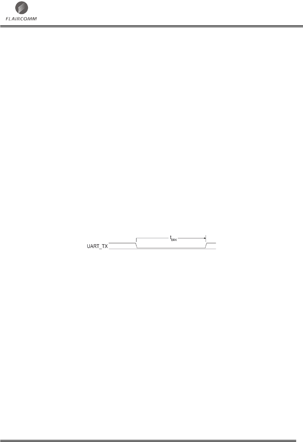
The UART interface resets BT of CBM202 on reception of a break signal. A break is identified by a
continuous logic low (0V) on the UART_RX terminal, as the figure below shows. If tBRK is longer
than the value, defined by the PSKEY_HOSTIO_UART_RESET_TIMEOUT, a reset occurs. This
feature enables a host to initialize the system to a known state. Also, BT of CBM202 can issue a
break character for waking the host.
Figure 3: UART_TX Timing
4.5.2.1 UART Configuration While Reset is Active
The UART interface is tri-state while the BT is being held in reset. This enables the user to daisy
chain devices onto the physical UART bus. The constraint on this method is that any devices
connected to this bus must tri-state when BT of CBM202 reset is de-asserted and the firmware
begins to run.
4.6 Audio Interface
CBM202 provides a digital audio interface for BT, which is configurable as wither PCM or I2S port.
4.6.1 PCM Interface
The audio PCM interface on the CBM202 supports:
Continuous transmission and reception of PCM encoded audio data over Bluetooth.
Processor overhead reduction through hardware support for continual transmission and
reception of PCM data
A bidirectional digital audio interface that routes directly into the baseband layer of the
firmware. It does not pass through the HCI protocol layer.
FLC-CBM202 Datasheet
Flaircomm Microelectronics Confidential
-20-
Hardware on the CBM202 for sending data to and from a SCO connection.
Up to 3 SCO connections on the PCM interface at any one time.
PCM interface master, generating PCM_SYNC and PCM_CLK.
PCM interface slave, accepting externally generated PCM_SYNC and PCM_CLK.
Various clock formats including:
Long Frame Sync
Short Frame Sync
GCI timing environments
13-bit or 16-bit linear, 8-bit μ-law or A-law commanded sample formats.
Receives and transmits on any selection of 3 of the first 4 slots following PCM_SYNC.
The PCM configuration options are enabled by setting the PS Key PSKEY_PCM_CONFIG32.
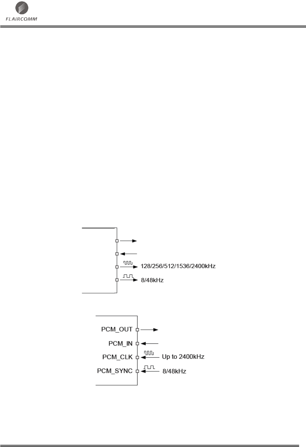
4.6.1.1 PCM Interface Master/Slave
When configured as the master of the PCM interface, CBM202 generates PCM_CLK and
PCM_SYNC.
PCM_OUT
PCM_CLK
PCM_IN
PCM_SYNC
Figure 4: PCM Interface Master
Figure 5: PCM Interface Slave
4.6.1.2 PCM_CLK and PCM_SYNC Generation
CBM202 has 2 methods of generating PCM_CLK and PCM_SYNC in master mode:

FLC-CBM202 Datasheet
Flaircomm Microelectronics Confidential
-21-
Generating these signals by DDS from CBM202 internal 4MHz clock. Using this mode limits
PCM_CLK to 128, 256 or 512 kHz and PCM_SYNC to 8 kHz.
Generating these signals by DDS from an internal 48MHz clock (which enables a greater range
of frequencies to be generated with low jitter but consumes more power). To select this second
method set bit 48M_PCM_CLK_GEN_EN in PSKEY_PCM_CONFIG32. When in this mode
and with long frame sync, the length of PCM_SYNC is either 8 or 16 cycles of PCM_CLK,
determined by LONG_LENGTH_SYNC_EN in PSKEY_PCM_CONFIG32.
The equation below describes PCM_CLK frequency when generated from the internal 48MHz clock:
24MHz
CNT_LIMIT
CNT_RATE
f
Set the frequency of PCM_SYNC relative to PCM_CLK using:
8SYNC_LIMIT
PCM_CLK
f
CNT_RATE, CNT_LIMIT and SYNC_LIMIT are set using SKEY_PCM_LOW_JITTER_CONFIG.
As an example, to generate PCM_CLK at 512 kHz with PCM_SYNC at 8 kHz, set
SKEY_PCM_LOW_JITTER_CONFIG to 0x08080177.
4.6.1.3 PCM Configuration
Configure the PCM by using the PS Keys, PSKEY_PCM_CONFIG32 and
SKEY_PCM_LOW_JITTER_CONFIG, see your PS Key file. The default for
SKEY_PCM_CONFIG32 is 0x00800000, i.e. first slot following sync is active, 13-bit linear voice
format, long frame sync and interface master generating 256 kHz PCM_CLK from 4MHz internal
clock with no tristate of PCM_OUT.
4.6.2 Digital Audio Interface (I²S)
The digital audio interface supports the industry standard formats for I²S, left-justified or right-
justified. The interface shares the same pins as the PCM interface, which means each audio bus is
mutually exclusive in its usage. Table below lists these alternative functions.
PCM Interface
I²S Interface
PCM_OUT
SD_OUT
PCM_IN
SD_IN
PCM_SYNC
WS
PCM_CLK
SCK
Table 4: PCM and I2S Digital Audio Interface
Configure the digital audio interface using the PSKEY_DIGITAL_AUDIO_CONFIG, see your PS
Key file.
FLC-CBM202 Datasheet
Flaircomm Microelectronics Confidential
-22-
5. Electrical Characteristic
5.1 WiFi Performance Specifications
5.1.1 DSSS and CCK modulations (802.11b) TX Performance Specifications
Characteristics
Min
Typical
Max
IEEE Specification
Unit
Frequency range
2400
-
2500
-
MHz
RMS transmit power(a)
16
18
20
-
dBm
RMS EVM
0
-28
-25
-9.1
dB
Spectral mask 1st Sidelobe
-
-39
-33
-30
dBr
Spectral mask 2nd Sidelobe
-
-54
-50
-50
dBr
RF carrier suppression
-
-30
-25
-15
dB
Center Frequency Tolerance
-20
2
+20
25
ppm
Occupied Bandwidth
-
22
-
-
MHz
Spurious
emissions
Frequency(GHz)
Min
Typical
Max
Band
dBm/Hz
0.076-0.108
-
-160
-
FM
0.776-0.794
-
-145
-
CDMA 2000
0.869-0.894
-
-145
-
GSM850/CDMA850
0.925-0.960
-
-143
-
GSM900
1.570-1.580
-
-135
-
GPS
1.805-1.880
-
-132
-
GSM1800/DCS1800
1.930-1.990
-
-130
-
GSM1900/CDMA1900
2.110-2.170
-
-125
-
W-CDMA 2000
Table 5: DSSS and CCK modulations (802.11b) TX Performance Specifications
5.1.2 OFDM TX Performance Specifications
Characteristics
Min
Typical
Max
IEEE Specification
Unit
Frequency range
2400
-
2500
-
MHz
RMS transmit power(a)
12
15
18
-
dBm
RMS EVM, 54Mbps
-
-28
-25
-25
dB
RMS EVM, mcs7
-
-29
-28
-28
dB
Spectral mask,±11MHz
-
-35
-30
-20
dBr
Spectral mask,±20MHz
-
-40
-30
-28
dBr
Spectral mask±30MHz
-
-50
-42
-40
dBr
Centre frequency leakage
-
-35
-25
-15
dB
Spectral flatness for spectral
lines -16 to -1,1 to 16
-
-
±2
±2
dB
FLC-CBM202 Datasheet
Flaircomm Microelectronics Confidential
-23-
Spectral flatness for spectral
lines -26 to -17,17 to 26
-
-
-4 to 2
-4 to 2
dB
Spurious emissions
Frequency(GHz)
Min
Typical
Max
dBm/Hz
0.076-0.108
-
-160
-
0.776-0.794
-
-145
-
0.869-0.894
-
-145
-
0.925-0.960
-
-143
-
1.570-1.580
-
-135
-
1.805-1.880
-
-132
-
1.930-1.990
-
-130
-
2.110-2.170
-
-125
-
Table 6: OFDM TX Performance Specifications
5.1.3 DSSS and CCK modulations (802.11b) RX Performance Specifications
Characteristics
Min
Typical
Max
IEEE Specification
Unit
Frequency range
2400
-
2500
-
MHz
Rx sensitivity,1Mbps DSSS(a)
-
-98
-90
-
dBm
Rx sensitivity,2Mbps DSSS(a)
-
-95
-88
-80
dBm
Rx sensitivity,5.5Mbps DSSS(a)
-
-91
-87
-
dBm
Rx sensitivity,11Mbps DSSS(a)
-
-90
-83
-76
dBm
Maximum input level, DSSS(a)
-4
0
-
-4
dBm
Maximum input level, CCK(a)
-5
-1
-
-10
dBm
Adjacent channel rejection, DSSS(b)
35
51
-
35
dB
Adjacent channel rejection, CCK(b)
35
48
-
35
dB
Out-of-band
blocking,
modulated
interferer
Frequency (GHz)
Min
Typical
Max
Band
Unit
0.776-0.794
-
24
-
CDMA 2000
dBm
0.824-0.849
-
19
-
GSM 850
0.824-0.849
-
16
-
CDMA 850
0.880-0.915
-
28
-
GSM 900
1.710-1.785
-
7
-
GSM1800/DCS1800
1.850-1.910
-
3
-
GSM1900/PCS1900
1.920-1.980
-
2
-
W-CDMA 2000
Table 7: DSSS and CCK modulations (802.11b) RX Performance Specifications
5.1.4 OFDM RX Performance Specifications
Characteristics
Min
Typical
Max
IEEE Specification
Unit
Frequency range
2400
-
2500
-
MHz

FLC-CBM202 Datasheet
Flaircomm Microelectronics Confidential
-24-
Rx sensitivity,6Mbps
-
-92
-84
-82
dBm
Rx sensitivity,9Mbps
-
-91
-82
-81
dBm
Rx sensitivity,12Mbps
-
-90
-82
-79
dBm
Rx sensitivity,18Mbps
-
-87
-78
-77
dBm
Rx sensitivity,24Mbps
-
-84
-76
-74
dBm
Rx sensitivity,36Mbps
-
-81
-73
-70
dBm
Rx sensitivity,48Mbps
-
-75
-69
-66
dBm
Rx sensitivity,54Mbps
-
-74
-68
-65
dBm
Rx sensitivity,MCS0
-
-92
-84
-82
dBm
Rx sensitivity, MCS1
-
-89
-81
-79
dBm
Rx sensitivity, MCS2
-
-87
-78
-77
dBm
Rx sensitivity, MCS3
-
-83
-76
-74
dBm
Rx sensitivity, MCS4
-
-80
-70
-70
dBm
Rx sensitivity, MCS5
-
-75
-66
-66
dBm
Rx sensitivity, MCS6
-
-74
-65
-65
dBm
Rx sensitivity, MCS7
-
-72
-64
-64
dBm
Maximum input level
-5
-1
-
-20
dBm
Adjacent channelrejection,6Mbps
16
27
-
16
dB
Adjacent channel rejection,9Mbps
15
26
-
15
dB
Adjacent channel rejection,12Mbps
13
25
-
13
dB
Adjacent channel rejection,18Mbps
11
25
-
11
dB
Adjacent channel rejection,24Mbps
8
23
-
8
dB
Adjacent channel rejection,36Mbps
4
20
-
4
dB
Adjacent channel rejection,48Mbps
0
16
-
0
dB
Adjacent channel rejection,54Mbps
-1
14
-
-1
dB
Adjacent channel rejection,MCS0
16
27
-
16
dB
Adjacent channel rejection,MCS1
13
25
-
13
dB
Adjacent channel rejection,MCS2
11
21
-
11
dB
Adjacent channel rejection,MCS3
8
22
-
8
dB
Adjacent channel rejection,MCS4
4
16
-
4
dB
Adjacent channel rejection,MCS5
0
13
-
0
dB
Adjacent channel rejection,MCS6
-1
10
-
-1
dB
Adjacent channel rejection,MCS7
-2
6
-
-2
dB
Out-of-band
blocking,
modulated
interferer
Frequency(GHz)
Min
Typ
Max
Band
Unit
0.776-0.794
-
18
-
CDMA 2000
dBm
0.824-0.849
-
17
-
GSM 850
0.824-0.849
-
14
-
CDMA 850
0.880-0.915
-
25
-
GSM900
FLC-CBM202 Datasheet
Flaircomm Microelectronics Confidential
-25-
1.710-1.785
-
1
-
GSM1800/DCS1800
1.850-1.910
-
0
-
GSM1900/PCS1900
1.920-1.980
-
-3
-
W-CDMA 2000
Table 8: OFDM RX Performance Specifications
5.2 Bluetooth Performance Specifications
5.2.1 Transmitter
Condition: VDD=1.8V, Temperature= +20°C .
Characteristics
Min
Typical
Max
BT Specification
Unit
Maximum RF transmit power (a)
-
6
7
4 to 20 Class 1
-6 to 4 Class 2
dBm
RF control range
25
30
-
≥16
dB
20 dB bandwidth for modulated carrier
-
790
1000
≤1000
kHz
Adjacent channel transmit power
F = F0 ± 2MHz
-
-35
-20
≤-20
dBm
Adjacent channel transmit power
F = F0 ± 3MHz
-
-45
-40
≤-40
dBm
Adjacent channel transmit power
F = F0 ± > 3MHz
-
-50
-40
≤-40
dBm
△f1avg Maximum Modulation
140
163
175
140< f1avg<175
kHz
△f2max Maximum Modulation
115
154
-
115
kHz
△f1avg /△f1avg
0.80
0.98
-
≥0.80
-
Initial carrier frequency tolerance
-75
5
75
≤75
kHz
Drift Rate
-
7
20
≤20
kHz/50us
Drift (single slot packet)
-
8
25
≤25
kHz
Drift (five slot packet)
-
9
40
≤40
kHz
2nd Harmonic Content
-
-60
-30
≤-30
dBm
3nd Harmonic Content
-
-45
-40
≤ -30
dBm
Emitted power in
cellular bands
measured at
unbalanced port
of the balun.
Output power
≤6dBm
Frequency(GHz)
Min
Typ
Max
CelluBand
Unit
0.869-0.894
-
-124
-
GSM 850
dBm/Hz
0.869-0.894
-
-128
-
CDMA 850
0.925-0.960
-
-128
-
GSM 900
1.570-1.58
-
-138
-
GPS
1.805-1.880
-
-133
-
GSM 1800/ DCS 1800
1.930-1.990
-
-135
-
PCS 1900
1.930-1.990
-
-134
-
GSM 1900
1.930-1.990
-
-134
-
CDMA 1900
FLC-CBM202 Datasheet
Flaircomm Microelectronics Confidential
-26-
2.110-2.170
-
-136
-
W-CDMA 2000
2.110-2.170
-
-136
-
W-CDMA 2000
Table 9: Transmitter
Note:
(a) The firmware can maintain the transmit power to be within the Bluetooth specification limits: class 1 or class 2.
5.2.2 Receiver
Condition: VDD=1.8V, Temperature= +20°C .
Frequency
Min
Typical
Max
BT Specification
Unit
Sensitivity at 0.1%
BER for all packet
types
2.402
-
-86.0
-
≤-70
dBm
2.441
-
-86.0
-
2.480
-
-86.0
-
Maximum received signal at 1.0% BER
-20
10
-
≥-20
dBm
Continuous power
required to block
Bluetooth
reception (for
input power of -67
dBm with 0.1%
BER) measured at
the unbalanced
port of the balun.
Frequency
Min
Typical
Max
BT Specification
Unit
30-2000
-10
0
-
≥-10
dBm
2000-2400
-27
0
-
≥-27
2500-3000
-27
0
-
≥-27
C/I co-channel
-
6
11
≤11
dB
Spurious output level
Continuous power
in cellular bands
required to block
Bluetooth
reception (for
input power of -
67dBm with
0.1%BER)
measured at
unbalanced port of
the balun.
Frequency
Min
Typical
Max
Cellular Band
Unit
0.824-0.849
-
0
-
GSM 850
dBm
0.824-0.849
-
-10
-
CDMA 850
0.880-0.915
-
-5
-
GSM 900
1.710-1.785
-
0
-
GSM 1800/DCS 1800
1.850-1.910
-
0
-
GSM 1900/PCS 1900
1.850-1.910
-
-7
-
CDMA 1900
1.920-1.980
-
-10
-
W-CDMA 1900
Continuous power
in cellular bands
required to block
Bluetooth
reception (for
input power of -
72dBm with
0.1BER) measured
at unbalanced port
of the balun.
0.824-0.849
-
-2
-
GSM 850
dBm
0.824-0.849
-
-12
-
CDMA 850
0.880-0.915
-
-7
-
GSM 900
1.710-1.785
-
0
-
GSM 1800/DCS 1800
1.850-1.910
-
0
-
GSM 1900/PCS 1900
1.850-1.910
-
-12
-
CDMA 1900
1.920-1.980
-
-14
-
W-CDMA 1900
Table 10: Receiver
FLC-CBM202 Datasheet
Flaircomm Microelectronics Confidential
-27-
5.3 DC Electrical Specifications
5.3.1 Absolute Maximum Ratings
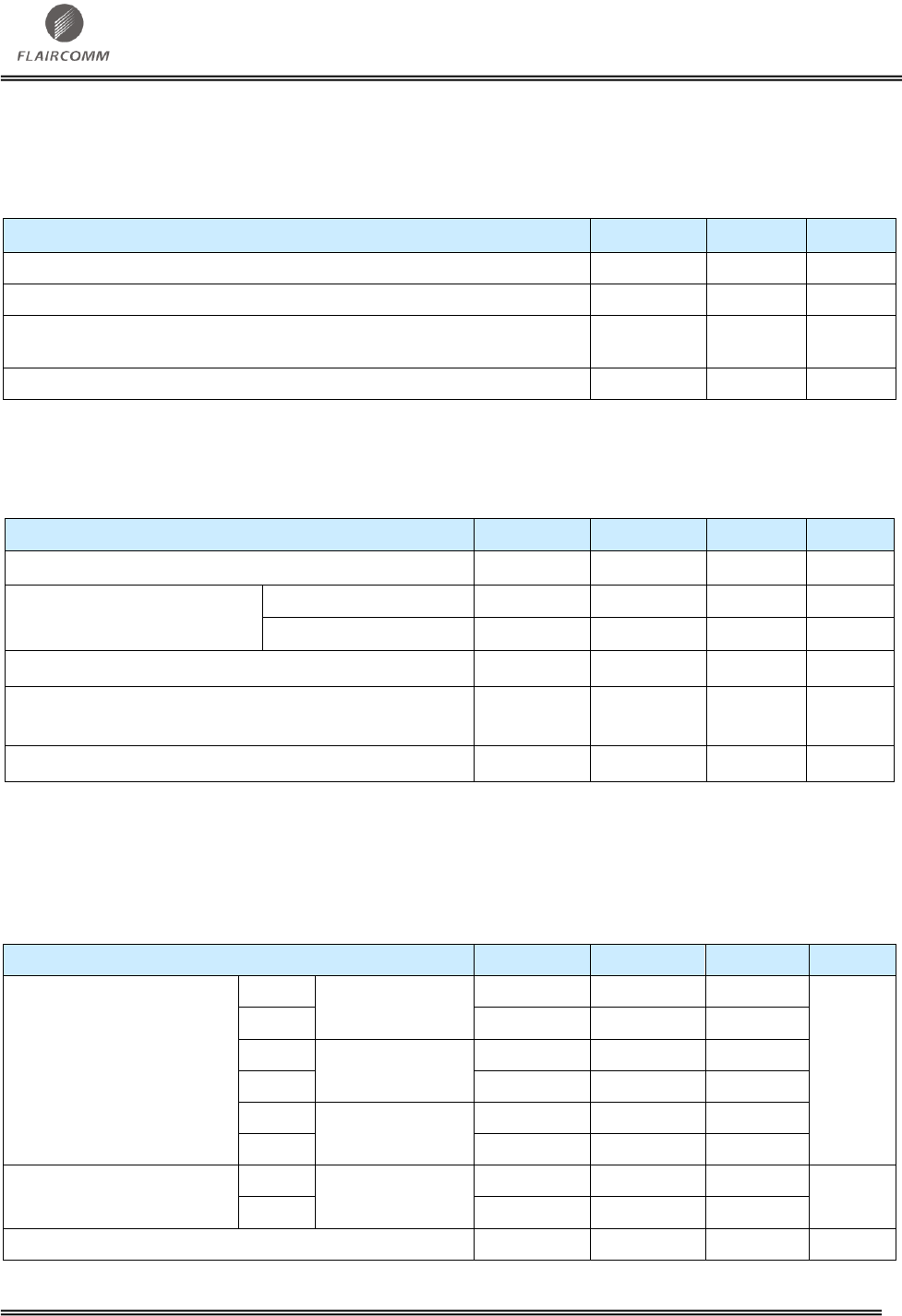
Table 11: Absolute Maximum Ratings
5.3.2 Recommended Operating Conditions
Operating Condition
Min
Typical
Max
Unit
Storage Temperature
-40
-
+85
°C
Operating Temperature Range
for A and I grade
-40
-
+85
°C
for V and C grade
-20
-
+70
°C
Host interface I/O supply voltage(VDD_SDIO)
1.7
-
3.6
V
Other I/O supply voltage(VDD_PADS_PIO_0_7,
VDD_AIO_PIO_8_15)
1.7
-
3.3
V
Linear regulator supply voltage 1.8V
1.75
-
1.95
V
Table 12: Recommended Operating Conditions
5.3.3 Current Consumption
5.3.3.1 WiFi Current Consumption
State
Min
Typical
Max
Unit
TX
3.3V
802.11b / 18dBm
-
190
-
mA
1.8V
100
3.3V
802.11g / 14dBm
145
1.8V
100
3.3V
802.11n / 14dBm
145
1.8V
100
RX
3.3V
802.11b,g,n
-
10
-
mA
1.8V
135
Leakage(deep sleep, including internal sleep clock )
-
69
-
μA
Table 13: WiFi Current Consumption
Rating
Min
Max
Unit
Storage Temperature
-40
+85
°C
Linear regulator voltage 1.8V
+1.45
+2.0
V
I/O supply voltage(VDD_SDIO, VDD_PADS_PIO_0_7,
VDD_AIO_PIO_8_15)
+1.7
+3.6
V
Other terminal voltages
VSS-0.3
VDD+0.3
V
FLC-CBM202 Datasheet
Flaircomm Microelectronics Confidential
-28-
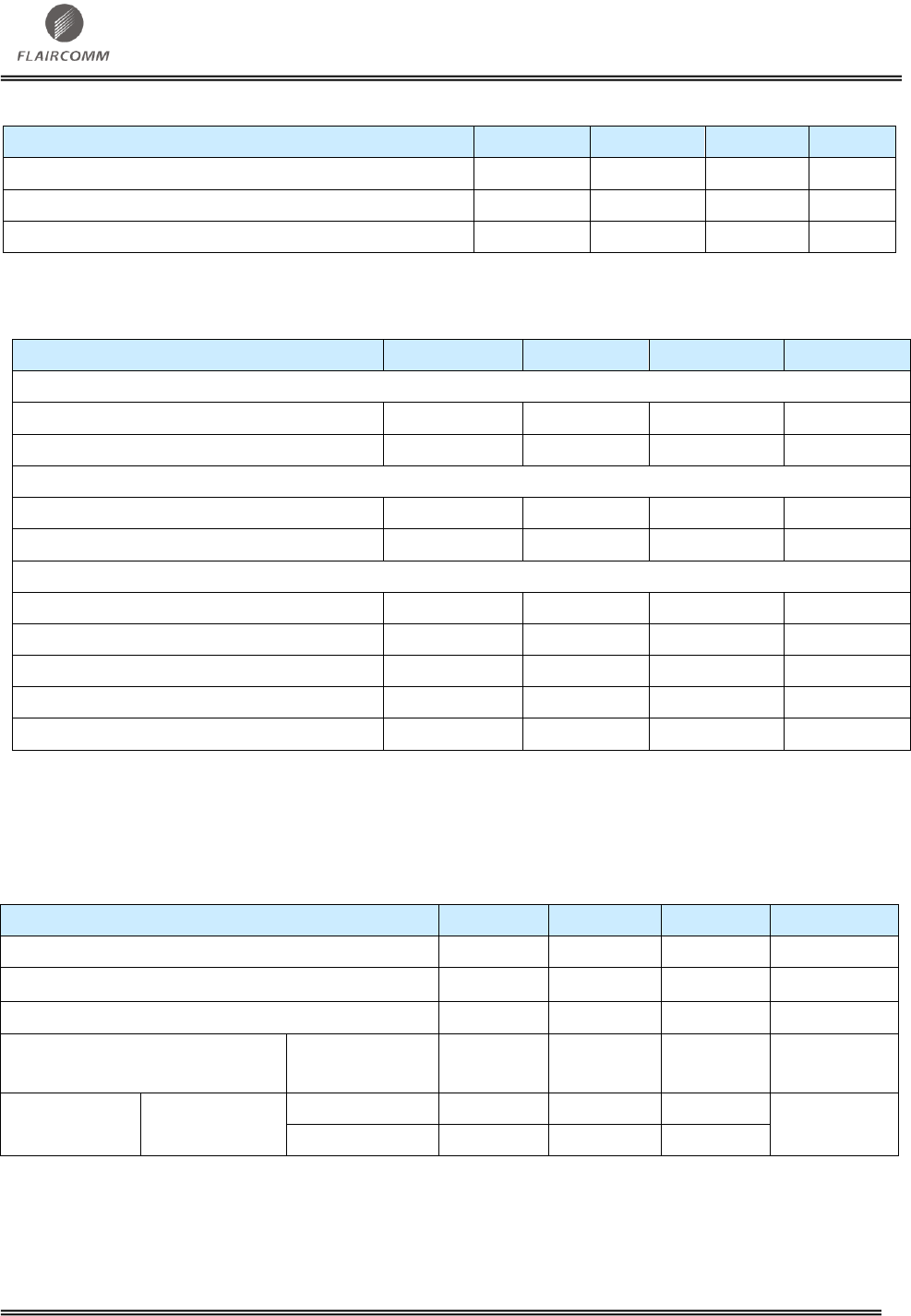
5.3.3.2 BT Current Consumption
State
Min
Typical
Max
Unit
Continuous receive
-
TBD
-
mA
Continuous transmit
-
TBD
-
mA
Leakage(deep sleep, including internal sleep clock )
-
TBD
-
μA
Table 14: BT Current Consumption
5.3.4 Digital Characteristics
Digital Terminals
Min
Typical
Max
Unit
Input Voltage Levels
VIL input logic level low
-0.3
-
0.25VDD
V
VIH input logic level high
0.625VDD
-
VDD+0.3
V
Output Voltage Levels
VOL output logic Level low, IOL=8.0mA
-
-
0.4
V
VOH output logic Level high, IOH=-8.0mA
0.75VDD
-
VDD
V
Input and Tri-state Currents
Strong pull-up
-150
-40
-10
μA
Strong pull-down
10
40
150
μA
Weak pull-up
-5
-1.0
-0.33
μA
Weak pull-down
0.33
1.0
5.0
μA
CI Input Capacitance
1.0
-
5.0
pF
Table 15: Digital Characteristics
5.3.5 Sleep Clock Characteristics
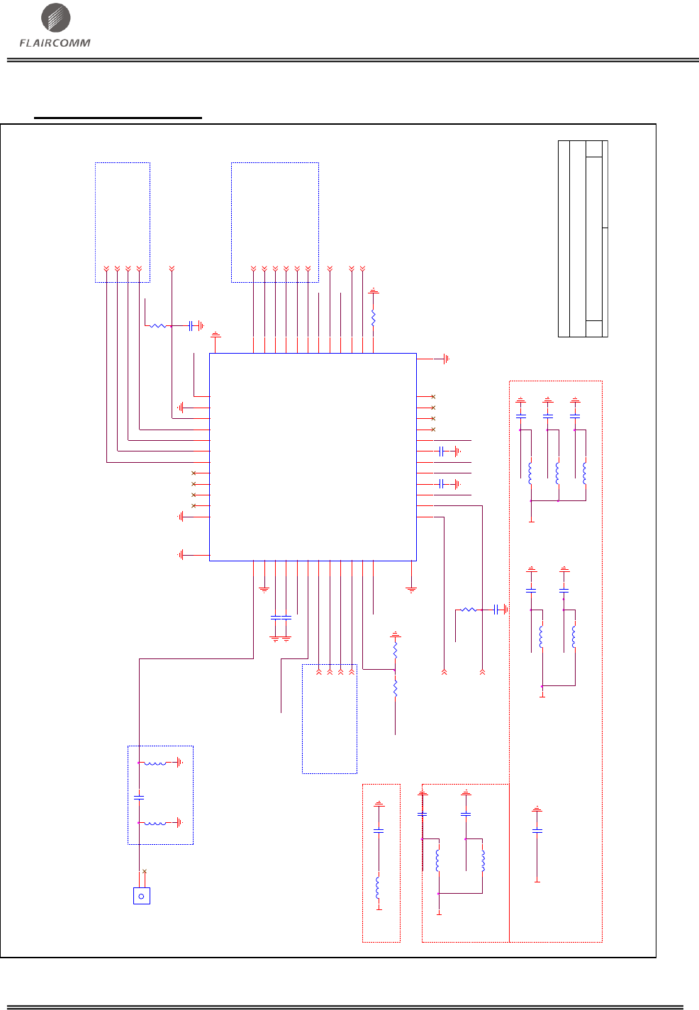
Sleep clock is an option with external 32.768 KHz clock for deep sleep and other low-power modes.
Following table lists the requirements for the sleep clock.
Sleep Clock
Min
Typical
Max
Unit
Frequency(a)
30
32.768
35
kHz
Frequency tolerance(b)
-
-
±250
ppm
Duty cycle
5:95
50:50
95:5
%
Jitter
Integrated rms jitter 10Hz to 20kHz
fref=32.768kHz
-
-
20
ns rms
Phase noise
fref=32.768kHz
1kHz offset
-
-
-100
dBc/Hz
10kHz offset
-
-
-120
Table 16: Sleep Clock Characteristics
(a) Stability is most important as frequency is calibrated against the system clock.
(b) The frequency of the slow clock is periodically calibrated against the system clock, as a result
the frequency is more important than the maximum deviation.

FLC-CBM202 Datasheet
Flaircomm Microelectronics Confidential
-29-
5.3.6 Power-on Reset Characteristics
Power-on Reset
Min
Typical
Max
Unit
Reset release on VDD_DIG rising(HL)
1.030
-
1.150
V
Reset assert on VDD_DIG falling(LO)
HL-0.060
-
HL-0.045
V
Reset assert on VDD_DIG falling(Sleep mode)
0.770
0.785
0.800
V
Table 17: Power-on Reset Characteristics
FLC-CBM202 Datasheet
Flaircomm Microelectronics Confidential
-30-
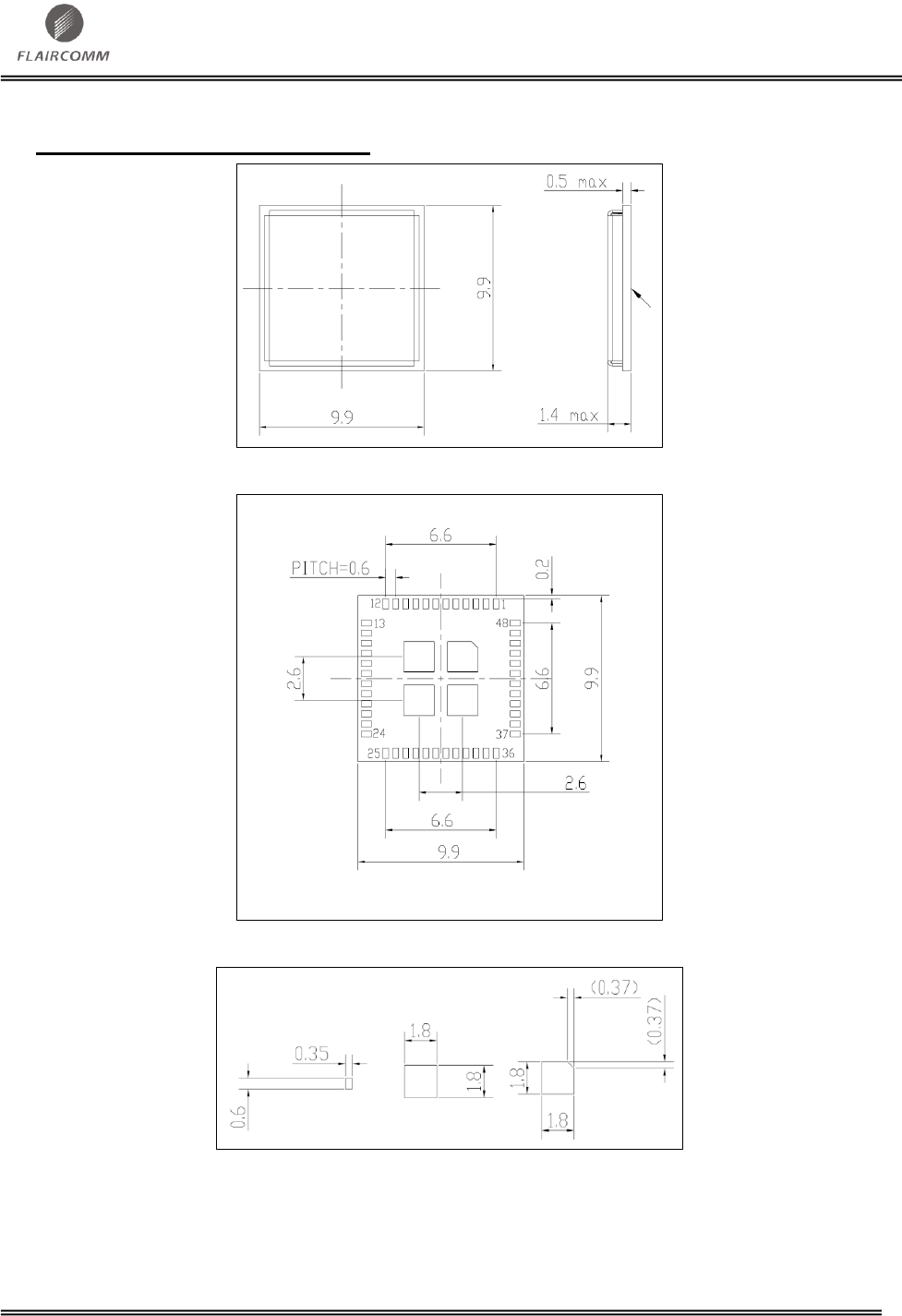
6. Reference Design
Figure 6: Reference Design
Title
Size Document Number Rev
Date: Sheet of
CBM202CL ref erence design <Rev Code>
CBM202CL
B
1 1Thursday , September 08, 2011
TCXO1.8
TCXO1.8V
WIFI_VDDIO
WIFI_SDIO3.3V
BT_1V8
BT_VDD_IO
1 2
L2
TBD
1 2
L1
TBD
1
2
2.4G_ANT
ALA931C5
R5 NC
BT_Sleep_CLK
L8 and L9 can be replaced by short circuits,
if BT1.8V is clean
BT1.8V
C9 TBD
L3, L4, L5, L6 and L7 can be replaced by short circuits,
if WIFI3.3V and WIFI1.8V are clean
C10
2.2uF
BT_PCM2_IN
BT_PCM2_CLK
BT_PCM2_SYNC
BT_PCM2_OUT
WIFI_SD_CMD
WIFI_SD_DATA[0]
WIFI_AIO[0]
WIFI_GPIO[9]
WIFI_SD_DATA[1]
WIFI_GPIO[10]
WIFI_SD_CLK
WIFI_SD_DATA[2]
WIFI_SD_DATA[3]
match
GND
2
WIFI_VDDRF3.3V 37
WIFI_AIO0 29
WIFI_nRESET 39
GND1 38
ANTENNA
1
GND2 48
BT_VDD_RF
4
BT_VDD_AUX
3
BT_SLEEP_CLK
6
BT_nRESET
14
BT_PCM2_OUT
7
BT_WAKEUP
13
BT_PCM2_CLK
9
BT_PCM2_IN
8
BT_SPI_PCM#_SEL
11
BT_PCM2_SYNC
10
BT_VDDIO
5
BT_UART_CTS 43
BT_UART_TX 40
TCXO1.8V
12
BT_VDD_DIG
16
BT_1.8V
15
BT_UART_RTS 42
BT_UART_RX 41
WIFI_VDDIO
20
WIFI_VDD_DIG
19
WIFI_VREG_IN_DIG1.8V
17
WIFI_SD_CMD 32
WIFI_SD_CLK 31
WIFI_SD_DATA3 33
WIFI_SD_DATA2 36
WIFI_SD_DATA1 35
WIFI_SD_DATA0 34
WIFI_VREG_IN_ANA1.8V 30
WIFI_GPIO9 27
WIFI_GPIO10 26
WIFI_VDDAIO3.3V 28
EEPROM_WP 25
WIFI_VDD_SDIO
18
WIFI_SPI_MOSI
22
WIFI_SPI_CS
21
WIFI_SPI_MISO
23
BT_PCM1_IN/SPI_MOSI 44
BT_PCM1_CLK/SPI_CLK 45
BT_PCM1_SYNC/SPI_CS 46
BT_PCM1_OUT/SPI_MISO 47
WIFI_SPI_CLK
24
GND3
49
GND4
50
GND5 51
GND6 52
U1
CBM202CL
C5 100nF
C3 2.2uF
BT_UART_CTS
BT_UART_RTS
BT_UART_TX
BT_UART_RX
WIFI_nRESET
C14 470nF
L4 BLM15AG121SN1
L6 BLM15AG121SN1
BT1.8V
WIFI_SDIO3.3V must be powered on
before the initialization of host SDIO bus
L5 BLM15AG121SN1
C8 2.2uF
L7 BLM15AG121SN1
WIFI1.8V
C6 2.2uF
L8 BLM15AG121SN1
WIFI3.3V
C7
2.2uF
C11 1uF
C13 330nF
BT1.8V
C15 2.2uF
L9 BLM15AG121SN1
C4 470nF
R3 NC
VREG_IN_ANA_1V8
R4 10K
C12 1uF
L3 BLM15AG121SN1
VREG_IN_DIG_1V8
C16 1uF
VREG_IN_ANA_1V8
WIFI_VDDAIO_3V3
WIFI_VDDIO
WIFI_SDIO3.3V
BT_1V8
VREG_IN_DIG_1V8
TCXO1.8
BT_VDD_IO
WIFI_VDD_RF_3V3 C1
2.2uF
C2
2.2uF
WIFI_VDD_RF_3V3
BT POWER
WIFI POWER
R2
10K
R1
10K
CLK POWER
WIFI_SDIO3.3V
WIFI1.8
WIFI SDIO
Interface
BT1.8V
BT UART
Interface
BT_WAKEUP
BT_nRESET
WIFI_VDDAIO_3V3
BT PCM
Interface
WIFI1.8
L11 BLM15AG121SN1
FLC-CBM202 Datasheet
Flaircomm Microelectronics Confidential
-31-
7. Mechanical Characteristic
Figure 7: Module Size (Top View and Side View)
Figure 8: Footprint (Top View)
Figure 9: Pin dimensions
FLC-CBM202 Datasheet
Flaircomm Microelectronics Confidential
-32-
8. Recommended PCB Layout and Mounting Pattern
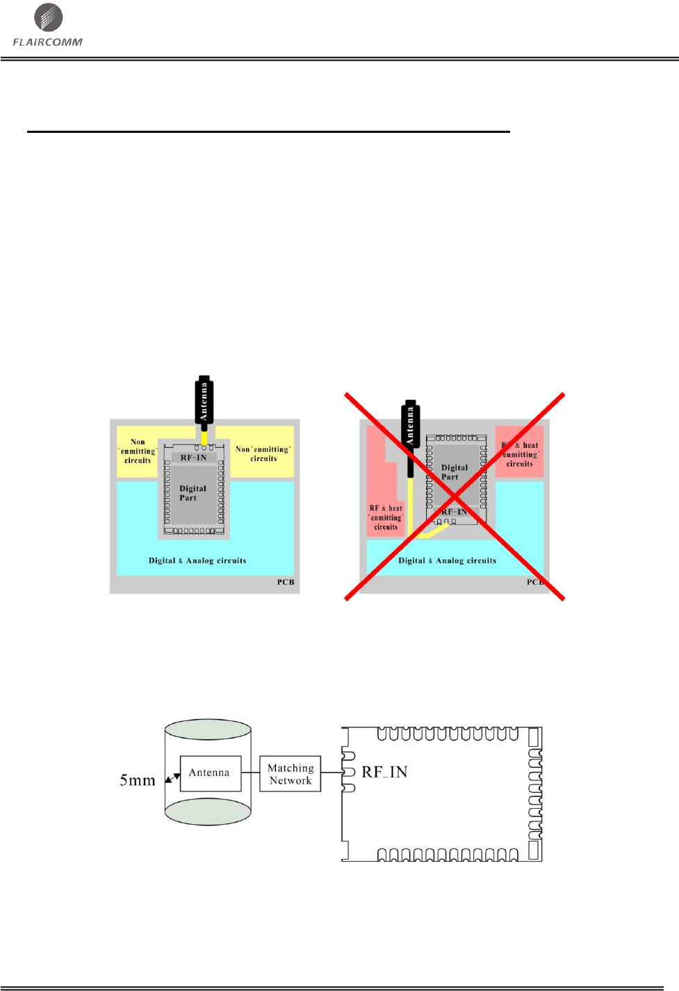
Placement and PCB layout are critical to optimize the performances of a module without on-board
antenna designs. The trace from the antenna port of the module to an external antenna should be 50
and must be as short as possible to avoid any interference into the transceiver of the module. The
location of the external antenna and RF-IN port of the module should be kept away from any noise
sources and digital traces. A matching network might be needed in between the external antenna and
Antenna port to better match the impedance to minimize the return loss.
As indicated in Figure 10, below, RF critical circuits of the module should be clearly separated from
any digital circuits on the system board. All RF circuits in the module are close to the antenna port.
The module, then, should be placed in this way that module digital part towards your digital section
of the system PCB.
Figure 10: Placement the Module on a System Board
8.1 Antenna Connection and Grounding Plane Design
Figure 11: Leave 5mm Clearance Space from the Antenna
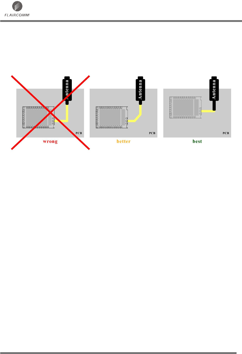
General design recommendations are:
The length of the trace or connection line should be kept as short as possible.
FLC-CBM202 Datasheet
Flaircomm Microelectronics Confidential
-33-
Distance between connection and ground area on the top layer should at least be as large as the
dielectric thickness.
Routing the RF close to digital sections of the system board should be avoided.
To reduce signal reflections, sharp angles in the routing of the micro strip line should be avoided.
Chamfers or fillets are preferred for rectangular routing; 45-degree routing is preferred over
Manhattan style 90-degree routing.
Figure 12: Recommended Trace Connects Antenna and the Module
Routing of the RF-connection underneath the module should be avoided.
Use as many vias as possible to connect the ground planes.
FLC-CBM202 Datasheet
Flaircomm Microelectronics Confidential
-34-
9. Recommended Reflow Profile
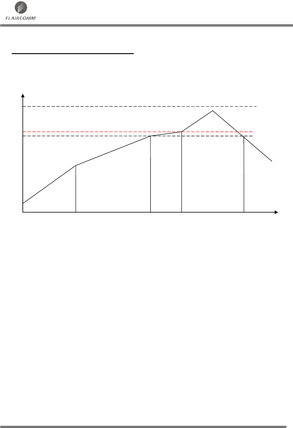
The soldering profile depends on various parameters necessitating a set up for each application. The
data here is given only for guidance on solder reflow.
210
217
℃
250
A
B
C
D
1
2
0
25
3
4
5
6
min
E
Figure 13: Recommended Reflow Profile
Pre-heat zone (A) — This zone raises the temperature at a controlled rate, typically 0.5 – 2 C/s.
The purpose of this zone is to preheat the PCB board and components to 120 ~ 150 C. This stage is
required to distribute the heat uniformly to the PCB board and completely remove solvent to reduce
the heat shock to components.
Equilibrium Zone 1 (B) — In this stage the flux becomes soft and uniformly encapsulates solder
particles and spread over PCB board, preventing them from being re-oxidized. Also with elevation
of temperature and liquefaction of flux, each activator and rosin get activated and start eliminating
oxide film formed on the surface of each solder particle and PCB board. The temperature is
recommended to be 150 to 210 for 60 to 120 second for this zone.
Equilibrium Zone 2 (c) (optional) — In order to resolve the upright component issue, it is
recommended to keep the temperature in 210 – 217 for about 20 to 30 second.
Reflow Zone (D) — The profile in the figure is designed for Sn/Ag3.0/Cu0.5. It can be a reference
for other lead-free solder. The peak temperature should be high enough to achieve good wetting but
not so high as to cause component discoloration or damage. Excessive soldering time can lead to
intermetallic growth which can result in a brittle joint. The recommended peak temperature (Tp) is
230 ~ 250 C. The soldering time should be 30 to 90 second when the temperature is above 217 C.
Cooling Zone (E) — The cooling ate should be fast, to keep the solder grains small which will give
a longerlasting joint. Typical cooling rate should be 4 C.
FLC-CBM202 Datasheet
Flaircomm Microelectronics Confidential
-35-
10. Ordering Information
10.1 Product Packaging Information
TBD
Figure 14: Product Packaging Information
10.2 Ordering information
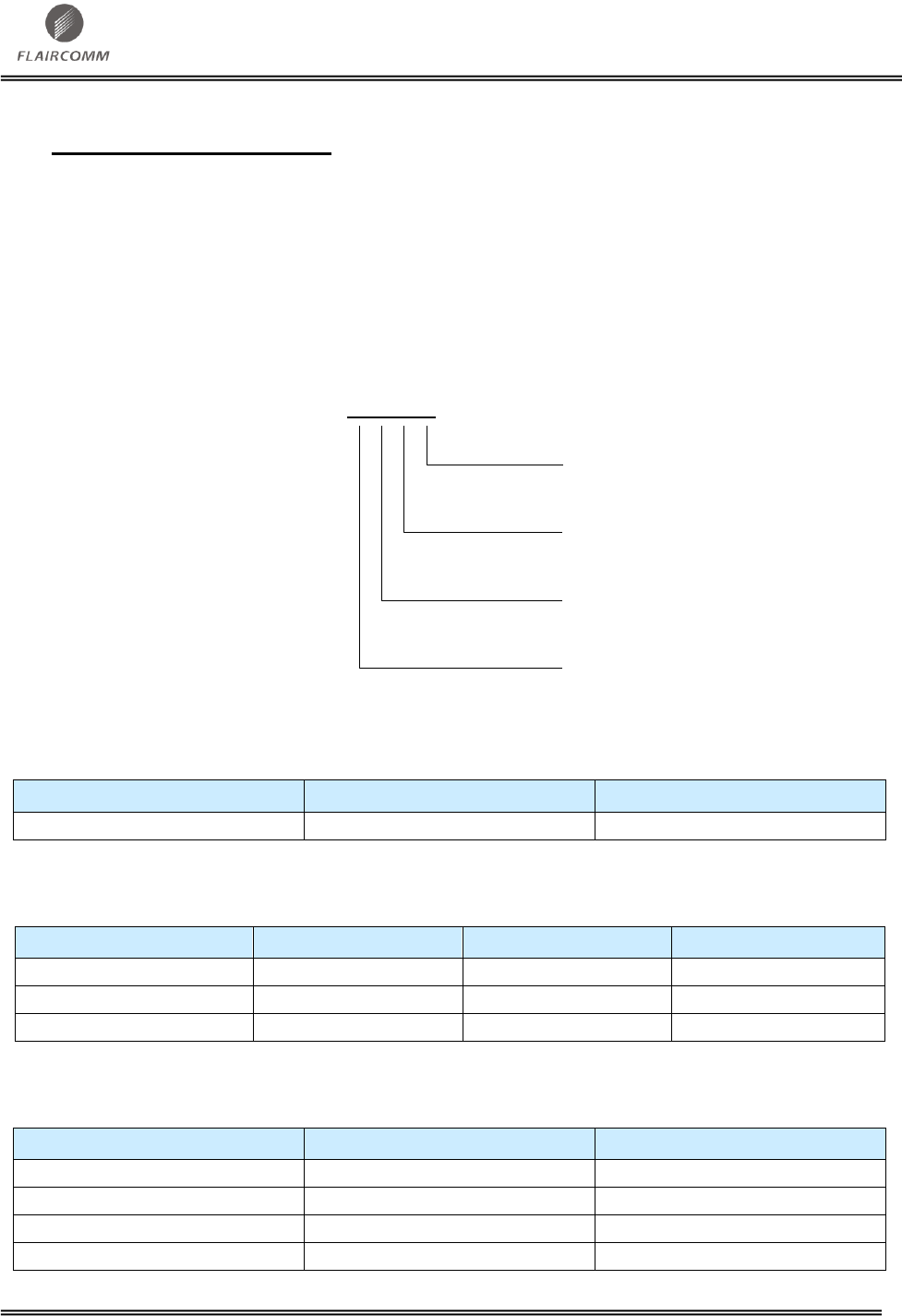
FLC-CBM202CL2A
Product Revision
Shipping Package
Product Package
Product Grade
Figure 15: Ordering Information
10.2.1 Product Revision
Product Revision
Description
Availability
A
Release A
Yes
Table 18: Product Revision
10.2.2 Shipping Package
Shipping Package
Description
Quantity
Availability
0
Foam Tray
—
No
1
Plastic Tray
—
No
2
Tape
TBD
Yes
Table 19: Shipping Package
10.2.3 Product Package
Product Package
Description
Availability
Q
QFN
No
L
LGA
Yes
B
BGA
No
C
Connector
No
Table 20: Product Package

FLC-CBM202 Datasheet
Flaircomm Microelectronics Confidential
-36-
10.2.4 Product Grade
Product Grade
Description
Availability
C
Consumer
Yes
I
Industrial
Yes
V
Automobile After-Market
Yes
A
Automobile Before-Market
No
Table 21: Product Grade

FLC-CBM202 Datasheet
Flaircomm Microelectronics Confidential
-37-
11. Cautions &Warnings
11.1 FCC Statement
1. This device complies with Part 15 of the FCC Rules. Operation is subject to the following two
conditions:
(1) This device may not cause harmful interference.
(2) This device must accept any interference received, including interference that may cause
undesired operation.
2. Changes or modifications not expressly approved by the party responsible for compliance could
void the user's authority to operate the equipment.
NOTE: This equipment has been tested and found to comply with the limits for a Class B digital
device, pursuant to Part 15 of the FCC Rules. These limits are designed to provide reasonable
protection against harmful interference in a residential installation.
This equipment generates uses and can radiate radio frequency energy and, if not installed and used
in accordance with the instructions, may cause harmful interference to radio communications.
However, there is no guarantee that interference will not occur in a particular installation. If this
equipment does cause harmful interference to radio or television reception, which can be determined
by turning the equipment off and on, the user is encouraged to try to correct the interference by one
or more of the following measures:
Reorient or relocate the receiving antenna.
Increase the separation between the equipment and receiver.
Connect the equipment into an outlet on a circuit different from that to which the receiver is
connected.
Consult the dealer or an experienced radio/TV technician for help.
This radio module must not be installed to co-locate and operate simultaneously with other radios in
host system; additional testing and equipment authorization may be required to operating
simultaneously with other radios.
11.2 FCC Radiation Exposure Statement
This equipment complies with FCC radiation exposure limits set forth for an uncontrolled
environment. This equipment should be installed and operated with minimum distance 20cm
between the radiator & your body.
11.3 FLC-CBM202 Label Instructions
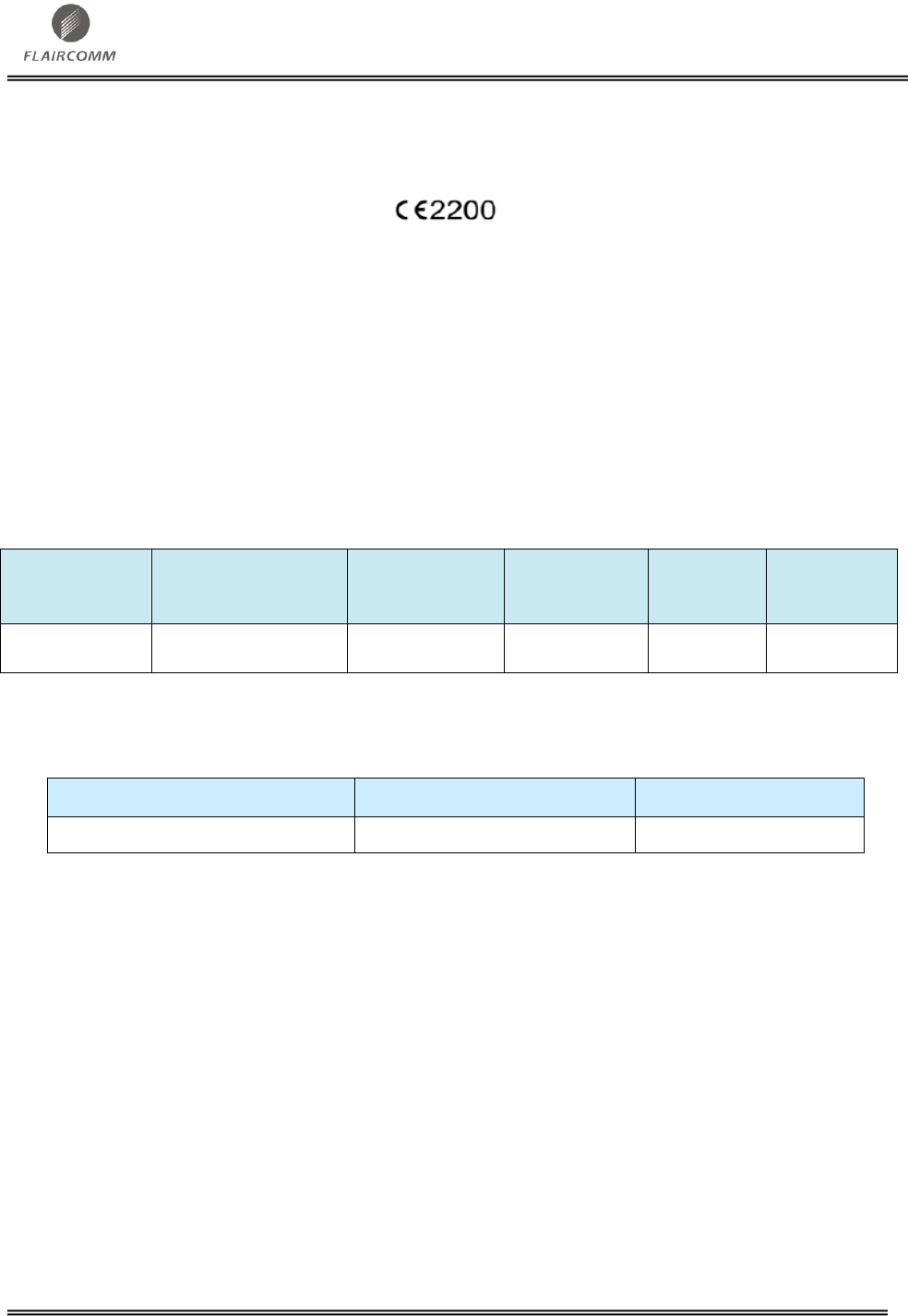
The FLC-CBM202 module is designed to comply with the FCC statements.
FLC-CBM202 Datasheet
Flaircomm Microelectronics Confidential
-38-
The packaging of host system that uses CBM202 should display a label indicating the information as
follows:
Contains FCC ID: P4ICBM202
Model: FLC-CBM202CL2A/FLC-CBM202IL2A/FLC-CBM202VL2A
Any similar wording that expresses the same meaning may also be used.
11.4 FLC-CBM202 Antenna Statement
11.4.1 Antenna Electrical Specifications
Part
Number
Frequency Range
(GHz)
Temperature
Average
Gain
VSWR
Impedance
ALA931C5
2.4~ 2.485
21.5°C typ.
-3 dBi min.
2.5:1 max.
50 Ω
Table 22: Antenna Electrical Specifications
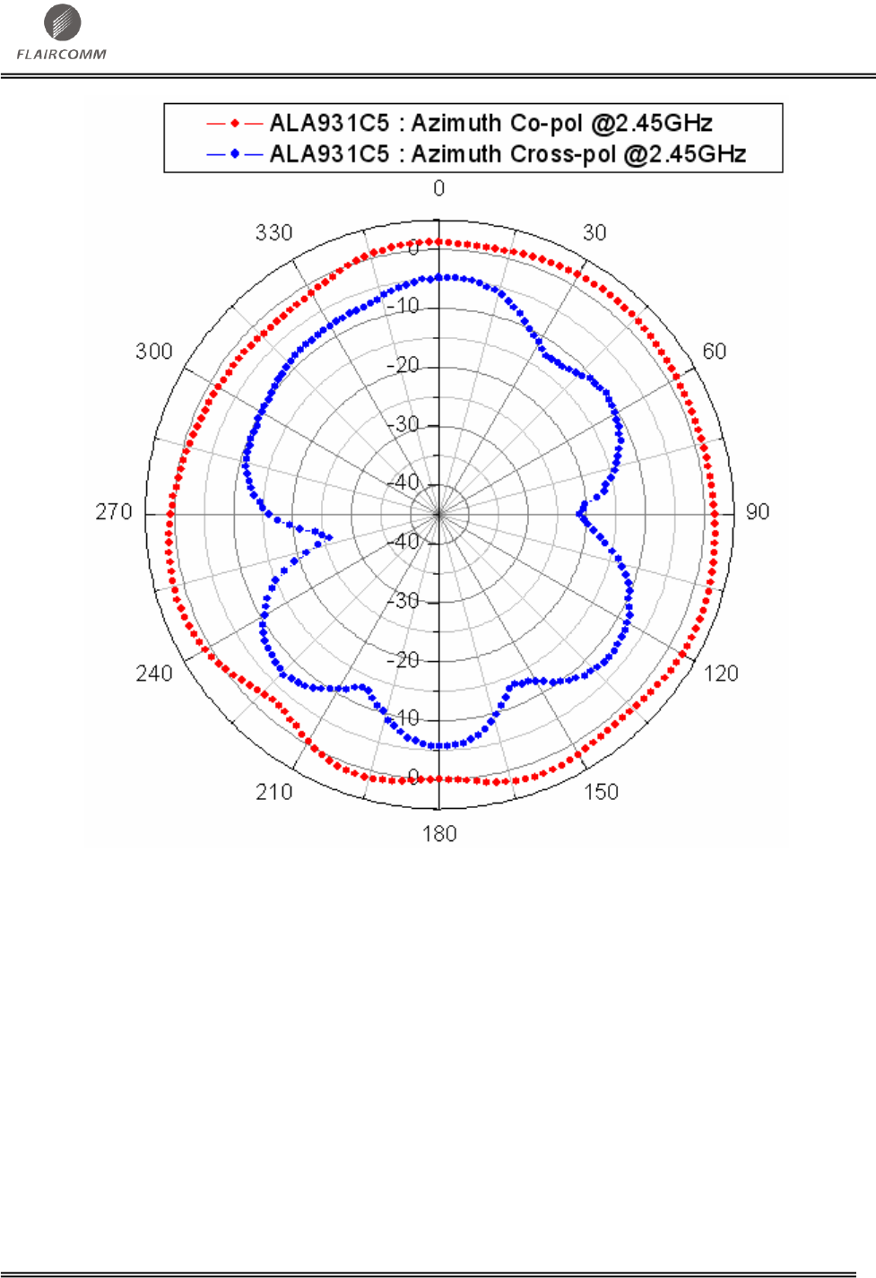
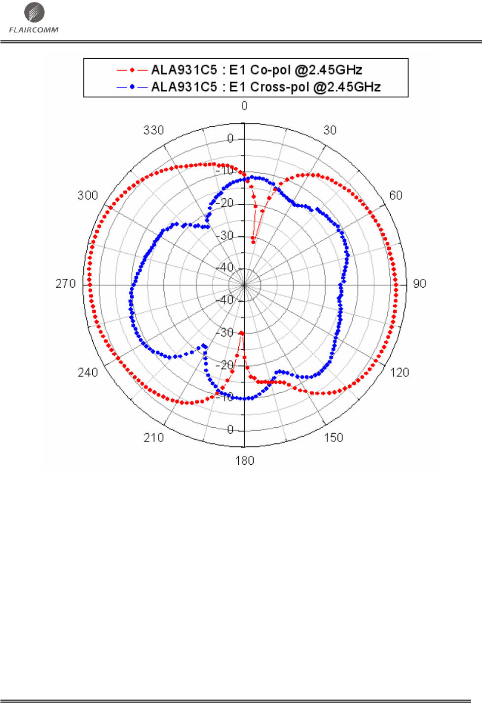
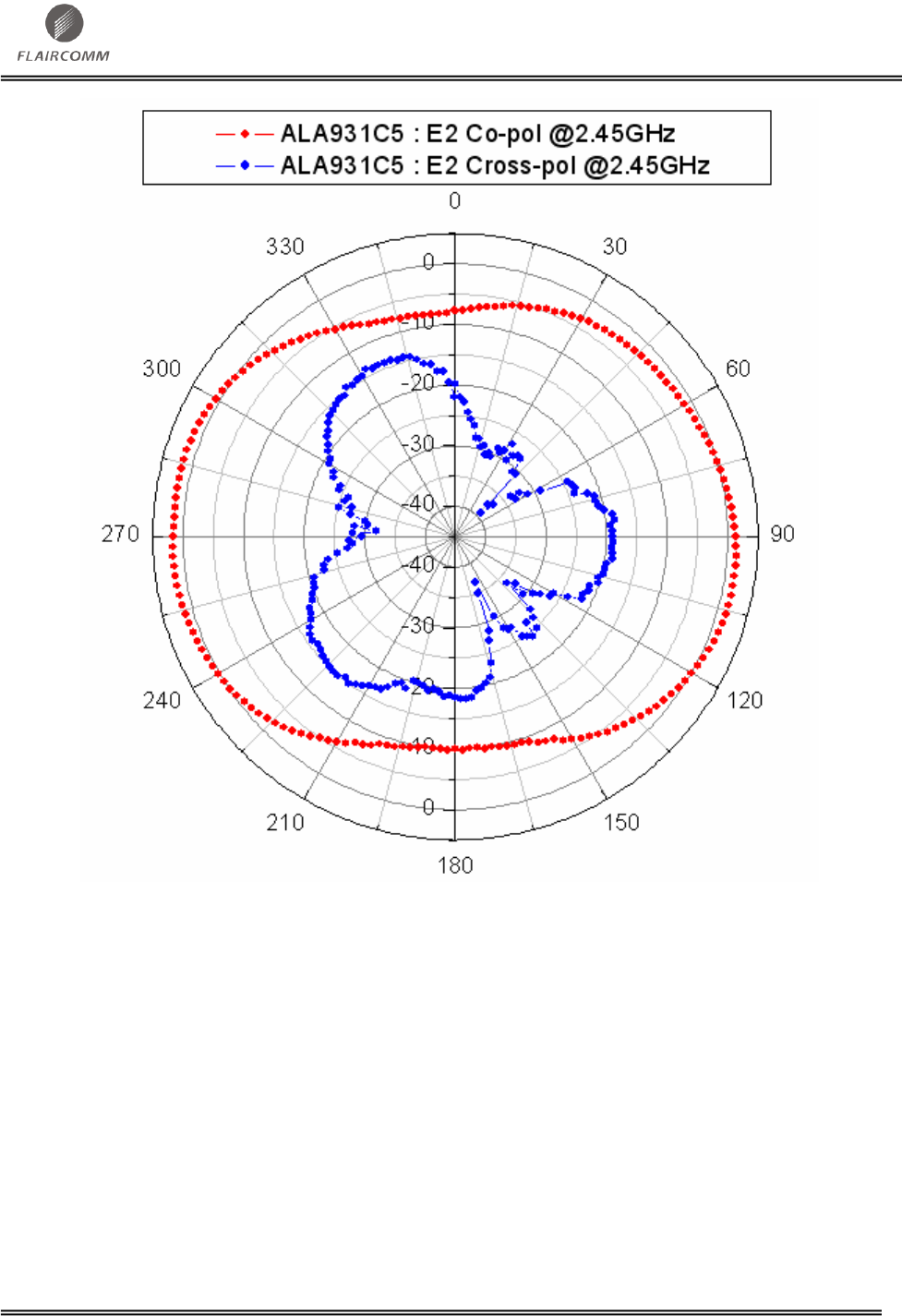
11.4.2 Radiation Gain and Pattern
Peak Gain(dBi)
Average Gain(dBi)
Remark
2.8
1.0
@2.45 GHz
Table 23: Radiation Gain and Pattern
FLC-CBM202 Datasheet
Flaircomm Microelectronics Confidential
-39-
Figure 16: ALA931C5 Radiation Pattern : Azimuth@2.45GHz
FLC-CBM202 Datasheet
Flaircomm Microelectronics Confidential
-40-
Figure 17: ALA931C5 Radiation Pattern : Elevation1@2.45GHz
FLC-CBM202 Datasheet
Flaircomm Microelectronics Confidential
-41-
Figure 18: ALA931C5 Radiation Pattern : Elevation2@2.45GHz