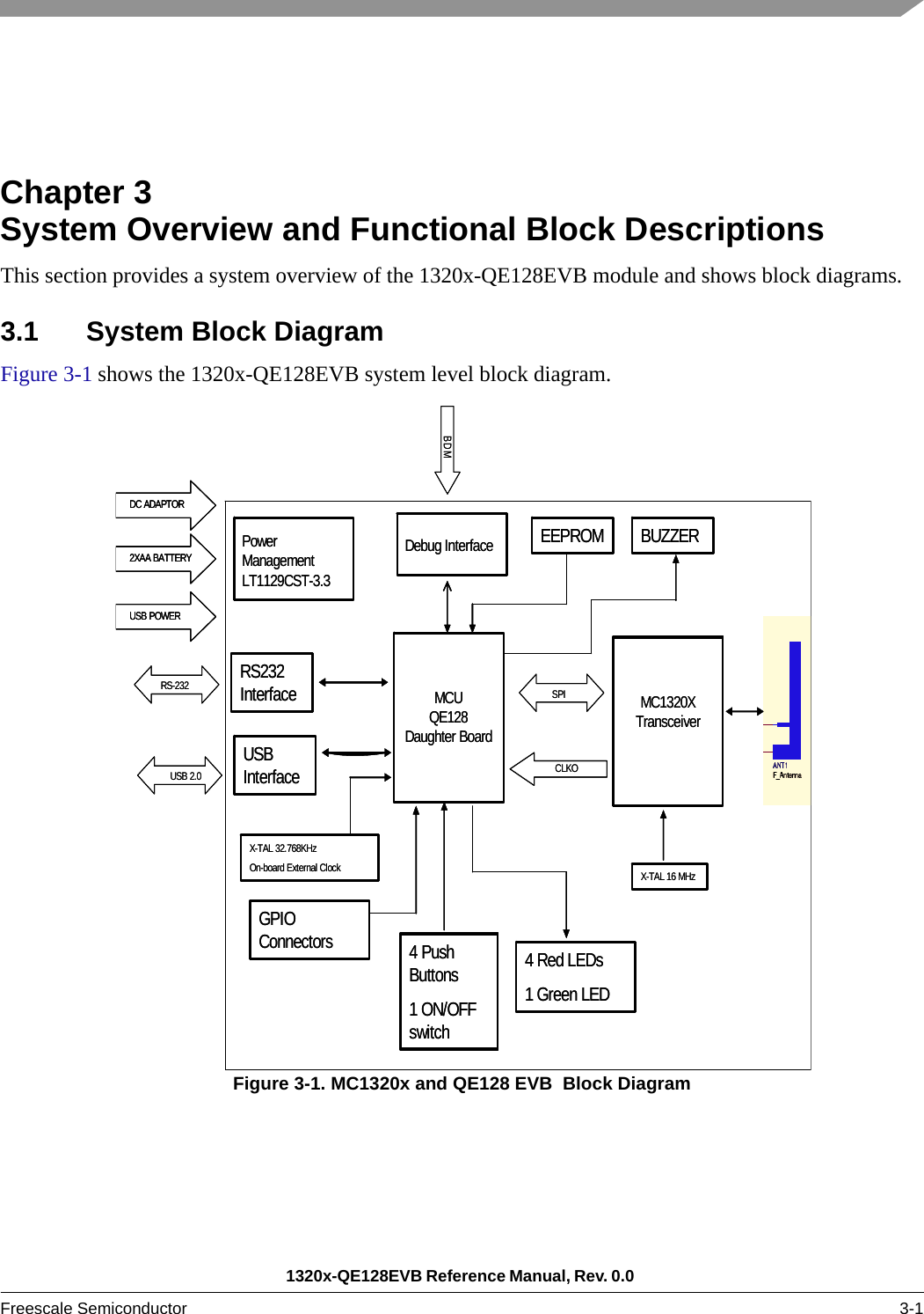
Freescale Semiconductor 1320X-QE128EVB IEEE 802.15.4 2.4 GHz ZigBee Evaluation Board User Manual

Freescale Semiconductor, Inc. IEEE 802.15.4 2.4 GHz ZigBee Evaluation Board

User Manual

Document Number: 1320xQE128EVBRMRev. 0.002/2008 1320x-QE128EVBReference Manual
  How to Reach Us:Home Page:www.freescale.comE-mail:support@freescale.comUSA/Europe or Locations Not Listed:Freescale SemiconductorTechnical Information Center, CH3701300 N. Alma School RoadChandler, Arizona 85224+1-800-521-6274 or +1-480-768-2130support@freescale.comEurope, Middle East, and Africa:Freescale Halbleiter Deutschland GmbHTechnical Information CenterSchatzbogen 781829 Muenchen, Germany+44 1296 380 456 (English)+46 8 52200080 (English)+49 89 92103 559 (German)+33 1 69 35 48 48 (French)support@freescale.comJapan:Freescale Semiconductor Japan Ltd.HeadquartersARCO Tower 15F1-8-1, Shimo-Meguro, Meguro-ku,Tokyo 153-0064, Japan0120 191014 or +81 3 5437 9125support.japan@freescale.comAsia/Pacific:Freescale Semiconductor Hong Kong Ltd.Technical Information Center2 Dai King StreetTai Po Industrial EstateTai Po, N.T., Hong Kong+800 2666 8080support.asia@freescale.comFor Literature Requests Only:Freescale Semiconductor Literature Distribution CenterP.O. Box 5405Denver, Colorado 802171-800-521-6274 or 303-675-2140Fax: 303-675-2150LDCForFreescaleSemiconductor@hibbertgroup.comInformation in this document is provided solely to enable system and software implementers to use Freescale Semiconductor products. There are no express or implied copyright licenses granted hereunder to design or fabricate any integrated circuits or integrated circuits based on the information in this document.Freescale Semiconductor reserves the right to make changes without further notice to any products herein. Freescale Semiconductor makes no warranty, representation or guarantee regarding the suitability of its products for any particular purpose, nor does Freescale Semiconductor assume any liability arising out of the application or use of any product or circuit, and specifically disclaims any and all liability, including without limitation consequential or incidental damages. “Typical” parameters that may be provided in Freescale Semiconductor data sheets and/or specifications can and do vary in different applications and actual performance may vary over time. All operating parameters, including “Typicals”, must be validated for each customer application by customer’s technical experts. Freescale Semiconductor does not convey any license under its patent rights nor the rights of others. Freescale Semiconductor products are not designed, intended, or authorized for use as components in systems intended for surgical implant into the body, or other applications intended to support or sustain life, or for any other application in which the failure of the Freescale Semiconductor product could create a situation where personal injury or death may occur. Should Buyer purchase or use Freescale Semiconductor products for any such unintended or unauthorized application, Buyer shall indemnify and hold Freescale Semiconductor and its officers, employees, subsidiaries, affiliates, and distributors harmless against all claims, costs, damages, and expenses, and reasonable attorney fees arising out of, directly or indirectly, any claim of personal injury or death associated with such unintended or unauthorized use, even if such claim alleges that Freescale Semiconductor was negligent regarding the design or manufacture of the part.Freescale™ and the Freescale logo are trademarks of Freescale Semiconductor, Inc. All other product or service names are the property of their respective owners. © Freescale Semiconductor, Inc. 2007, 2008. All rights reserved.
1320x-QE128EVB Reference Manual, Rev. 0.0Freescale Semiconductor i ContentsAbout This BookAudience . . . . . . . . . . . . . . . . . . . . . . . . . . . . . . . . . . . . . . . . . . . . . . . . . . . . . . . . . . . . . . . . . . . .  iiiOrganization . . . . . . . . . . . . . . . . . . . . . . . . . . . . . . . . . . . . . . . . . . . . . . . . . . . . . . . . . . . . . . . . .  iiiRevision History . . . . . . . . . . . . . . . . . . . . . . . . . . . . . . . . . . . . . . . . . . . . . . . . . . . . . . . . . . . . . .  iiiChapter 1 Safety Information1.1 FCC Guidelines. . . . . . . . . . . . . . . . . . . . . . . . . . . . . . . . . . . . . . . . . . . . . . . . . . . . . . . . . . . . . .  1-11.2 Disposal Instructions. . . . . . . . . . . . . . . . . . . . . . . . . . . . . . . . . . . . . . . . . . . . . . . . . . . . . . . . . .  1-1Chapter 2 1320x-QE128EVB Module Overview and Description2.1 Introduction. . . . . . . . . . . . . . . . . . . . . . . . . . . . . . . . . . . . . . . . . . . . . . . . . . . . . . . . . . . . . . . . .  2-12.2 Features. . . . . . . . . . . . . . . . . . . . . . . . . . . . . . . . . . . . . . . . . . . . . . . . . . . . . . . . . . . . . . . . . . . .  2-22.3 Board Level Specifications. . . . . . . . . . . . . . . . . . . . . . . . . . . . . . . . . . . . . . . . . . . . . . . . . . . . .  2-3Chapter 3 System Overview and Functional Block Descriptions3.1 System Block Diagram . . . . . . . . . . . . . . . . . . . . . . . . . . . . . . . . . . . . . . . . . . . . . . . . . . . . . . . .  3-13.2 System Overview . . . . . . . . . . . . . . . . . . . . . . . . . . . . . . . . . . . . . . . . . . . . . . . . . . . . . . . . . . . .  3-23.2.1 MC9S08QE128 MCU Module . . . . . . . . . . . . . . . . . . . . . . . . . . . . . . . . . . . . . . . . . . . . . . .  3-23.2.2 MC1320x IEEE 802.25.4 Transceiver . . . . . . . . . . . . . . . . . . . . . . . . . . . . . . . . . . . . . . . . .  3-33.2.3 1320x-QE128EVB System Functions  . . . . . . . . . . . . . . . . . . . . . . . . . . . . . . . . . . . . . . . . .  3-43.3 Power Management and Measurement. . . . . . . . . . . . . . . . . . . . . . . . . . . . . . . . . . . . . . . . . . . .  3-53.4 Low-cost 2.4 GHz IEEE 802.15.4 ISM Band Radio . . . . . . . . . . . . . . . . . . . . . . . . . . . . . . . . .  3-53.5 Interfaces. . . . . . . . . . . . . . . . . . . . . . . . . . . . . . . . . . . . . . . . . . . . . . . . . . . . . . . . . . . . . . . . . . .  3-63.5.1 USB Interface . . . . . . . . . . . . . . . . . . . . . . . . . . . . . . . . . . . . . . . . . . . . . . . . . . . . . . . . . . . .  3-63.5.2 16x2 Monochrome Character LCD Display. . . . . . . . . . . . . . . . . . . . . . . . . . . . . . . . . . . . .  3-73.5.3 Debug/Development Interface . . . . . . . . . . . . . . . . . . . . . . . . . . . . . . . . . . . . . . . . . . . . . . .  3-73.5.4 RS232 Interface  . . . . . . . . . . . . . . . . . . . . . . . . . . . . . . . . . . . . . . . . . . . . . . . . . . . . . . . . . .  3-73.6 GPIO Connectors . . . . . . . . . . . . . . . . . . . . . . . . . . . . . . . . . . . . . . . . . . . . . . . . . . . . . . . . . . . .  3-73.7 Clocks . . . . . . . . . . . . . . . . . . . . . . . . . . . . . . . . . . . . . . . . . . . . . . . . . . . . . . . . . . . . . . . . . . . . .  3-8Chapter 4 Interface Locations and Pinouts4.1 Overview. . . . . . . . . . . . . . . . . . . . . . . . . . . . . . . . . . . . . . . . . . . . . . . . . . . . . . . . . . . . . . . . . . .  4-14.2 Power Management  . . . . . . . . . . . . . . . . . . . . . . . . . . . . . . . . . . . . . . . . . . . . . . . . . . . . . . . . . .  4-24.2.1 Supply Sources . . . . . . . . . . . . . . . . . . . . . . . . . . . . . . . . . . . . . . . . . . . . . . . . . . . . . . . . . . .  4-24.2.2 On/Off Switch (Hardware Reset) . . . . . . . . . . . . . . . . . . . . . . . . . . . . . . . . . . . . . . . . . . . . .  4-24.2.3 Power On Indicator. . . . . . . . . . . . . . . . . . . . . . . . . . . . . . . . . . . . . . . . . . . . . . . . . . . . . . . .  4-24.2.4 Power Measurement . . . . . . . . . . . . . . . . . . . . . . . . . . . . . . . . . . . . . . . . . . . . . . . . . . . . . . .  4-3
1320x-QE128EVB Reference Manual, Rev. 0.0ii Freescale Semiconductor 4.3 MC9S08QE128 MCU Module . . . . . . . . . . . . . . . . . . . . . . . . . . . . . . . . . . . . . . . . . . . . . . . . . .  4-34.4 RF Circuitry  . . . . . . . . . . . . . . . . . . . . . . . . . . . . . . . . . . . . . . . . . . . . . . . . . . . . . . . . . . . . . . . .  4-34.5 USB Connector (“B” Receptacle). . . . . . . . . . . . . . . . . . . . . . . . . . . . . . . . . . . . . . . . . . . . . . . . 4-34.6 LCD Connector. . . . . . . . . . . . . . . . . . . . . . . . . . . . . . . . . . . . . . . . . . . . . . . . . . . . . . . . . . . . . .  4-34.7 LEDs and Switches. . . . . . . . . . . . . . . . . . . . . . . . . . . . . . . . . . . . . . . . . . . . . . . . . . . . . . . . . . .  4-44.8 Debug/Development Connector (BDM Interface) . . . . . . . . . . . . . . . . . . . . . . . . . . . . . . . . . . .  4-44.9 RS232-Compatible UART Connector . . . . . . . . . . . . . . . . . . . . . . . . . . . . . . . . . . . . . . . . . . . .  4-54.10 GPIO Connectors . . . . . . . . . . . . . . . . . . . . . . . . . . . . . . . . . . . . . . . . . . . . . . . . . . . . . . . . . . . .  4-54.11 Jumper Selection. . . . . . . . . . . . . . . . . . . . . . . . . . . . . . . . . . . . . . . . . . . . . . . . . . . . . . . . . . . . .  4-7Chapter 5 Schematic and Bill of Material5.1 Schematic . . . . . . . . . . . . . . . . . . . . . . . . . . . . . . . . . . . . . . . . . . . . . . . . . . . . . . . . . . . . . . . . . .  5-15.2 Bill of Materials . . . . . . . . . . . . . . . . . . . . . . . . . . . . . . . . . . . . . . . . . . . . . . . . . . . . . . . . . . . . .  5-6
1320x-QE128EVB Reference Manual, Rev. 0.0 Freescale Semiconductor iii About This BookThis manual describes Freescale’s MC1320x and MC9S08QE128 evaluation board (1320x-QE128EVB). The 1320x-QE128EVB contains Freescale’s MC13202 QFN-32 package and MC9S08QE128 Daughter card used in the DEMOQE128 Flexis™ QE128 Demonstration Board. The MC13202 is a short range, low power 2.4 GHz Industrial, Scientific, and Medical (ISM) band transceiver. The MC13202 contains a complete 802.15.4 physical layer (PHY) modem designed for the IEEE® 802.15.4 standard which supports peer-to peer, star, and mesh networking. The MC9S08QE128 is a low cost, low power, high-performance HCS08 Family of 8-bit microcontroller units. The MC9S08QE128 use the enhanced HCS08 core with 128 Flash size and 64 pin LQFP package.AudienceThis manual is intended for system designers.OrganizationThis document is organized into five chapters.Chapter 1 Safety Information — This chapter highlights Federal Communications Commission operating guidelines.Chapter 2 MC1320x and QE128 EVB  Module Overview and Description — This chapter introduces MC1320x and QE128 EVB which is an IEEE, 802.15.4 compliant evaluation board based on the Freescale MC1320x and QE128 EVB device. Chapter 3 System Overview and Functional Block Descriptions — This section provides an overview of the  and system block diagrams.Chapter 4 Interface Locations and Pinouts — This chapter provides a description of the interface locations and pinout of the 1320x-QE128EVB circuit board. Chapter 5 Schematic and Bill of Materials — This chapter provides the schematic and Bill of Materials (BOM).Revision HistoryThe following table summarizes revisions to this document since the previous release (Rev 0.0).Revision HistoryLocation RevisionEntire Document First draft of this doc.
1320x-QE128EVB Reference Manual, Rev. 0.0 iv Freescale Semiconductor Definitions, Acronyms, and AbbreviationsThe following list defines the acronyms and abbreviations used in this document. ADC Analog to Digital ConverterCTS Clear to SendI2C Inter-Integrated Circuit is a multi-master serial computer busISM Industrial Scientific Medical 2.4 GHz radio frequency bandMAC Media Access ControllerMCU Microcontroller UnitPCB Printed circuit boardRTS Request to SendSPI Serial Peripheral InterfaceSSI Synchronous Serial InterfaceUSB Universal Serial Bus
1320x-QE128EVB Reference Manual, Rev. 0.0 Freescale Semiconductor 1-1Chapter 1  Safety Information1.1 FCC GuidelinesAny modifications to this product may violate the rules of the Federal Communications Commission and make operation of the product unlawful.1.1.1 47 C.F.R. Sec. 15.21This equipment has been tested and found to comply with the limits for a Class B digital device, pursuant to part 15 of the FCC Rules. These limits are designed to provide reasonable protection against harmful interference in a residential installation. This equipment generates, uses and can radiate radio frequency energy and, if not installed and used in accordance with the instructions, may cause harmful interference to radio communications. However, there is no guarantee that interference will not occur in a particular installation.  If this equipment does cause harmful interference to radio or television reception, which can be determined by turning the equipment off and on, the user is encouraged to try to correct the interference by one or more of the following measures:• Reorient or relocate the receiving antenna.• Increase the separation between the equipment and receiver.• Connect the equipment into an outlet on a circuit different from that to which the receiver is connected.• Consult the dealer or an experienced radio/TV technician for help.1.1.2 47 C.F.R. Sec.15.105(b)This equipment complies with FCC radiation exposure limits set forth for an uncontrolled environment. The antenna(s) used for this equipment must be installed to provide a separation distance of at least 8 inches (20cm) from all persons.This device complies with Part 15 of the FCC Rules.  Operation is subject to the following two conditions:1. This device may not cause harmful interference.2. This device must accept any interference received, including interference that may cause undesired operation.3. This device is susceptible to electrostatic discharge (ESD) and surge phenomenon.
Safety Information1320x-QE128EVB Reference Manual, Rev. 0.0 1-2 Freescale Semiconductor1.1.3 47 C.F.R. Sec.15.203An intentional radiator shall be designed to ensure that no antenna other than that furnished by the responsible party shall be used with the device.  The use of a permanently attached antenna or of an antenna that uses a unique coupling to the intentional radiator shall be considered sufficient to comply with the provisions of this Section.  The manufacturer may design the unit so that a broken antenna can be replaced by the user, but the use of a standard antenna jack or electrical connector is prohibited.  This requirement does not apply to carrier current devices or to devices operated under the provisions of Sections 15.211, 15.213, 15.217, 15.219, or 15.221.  Further, this requirement does not apply to intentional radiators that must be professionally installed, such as perimeter protection systems and some field disturbance sensors, or to other intentional radiators which, in accordance with Section 15.31(d), must be measured at the installation site.  However, the installer shall be responsible for ensuring that the proper antenna is employed so that the limits in this Part are not exceeded. 1.2 Disposal InstructionsThis product may be subject to special disposal requirements. For product disposal instructions, refer to www.freescale.com/productdisposal.
1320x-QE128EVB Reference Manual, Rev. 0.0 Freescale Semiconductor 2-1Chapter 2  1320x-QE128EVB Module Overview and Description2.1 IntroductionThe 1320x-QE128EVB is an evaluation board for developing IEEE® 802.15.4/ZigBee® software and applications ranging from simple proprietary point-to-point connectivity to complete ZigBee mesh networking on the QE microcontroller platform. The Freescale QE Microcontroller Family is unique in that the user can use an 8-bit CPU or a 32-bit CPU in a pin-compatible package and also retain the exact same peripheral and IO set. The 1320x-QE128EVB uses the MC9S08QE128 Microcontroller unit which is the first device of the pin-compatible 8-bit and 32-bit duo in the Flexis Series family. The Flexis series of controllers is the connection point of the Freescale Controller Continuum, delivering 8- and 32-bit compatibility for migration flexibility.The 1320x-QE128EVB evaluation board is based on the Freescale MC1320x transceiver and MC9S08QE128 Microcontroller unit (which is supplied as a daughter card). The 1320x-QE128EVB provides a platform to evaluate the MC1320x and MC9S08QE128 devices, develop software and applications, and demonstrate IEEE 802.15.4 and ZigBee networking capabilities. The evaluation board is supported by Freescale’s BeeKit software design environment for IEEE 802.15.4/ZigBee applications.Figure 2-1. 1320x-QE128EVB
1320x-QE128EVB Module Overview and Description1320x-QE128EVB Reference Manual, Rev. 0.0 2-2 Freescale Semiconductor2.2 FeaturesThe 1320x-QE128EVB provides the following features:• Uses MC9S08QE128 MCU Daughter card - supports the 9S08 based version of the QE128• Full IEEE 802.15.4 compliant wireless node; ZigBee capable with Freescale’s BeeStack software stack• Based on Freescale’s MC13202 transceiver in RF single-port mode— Printed F-antenna— Typical RX sensitivity of -92 dBm at 1.0% Packet Error Rate— Typical 0 dBm up to 3.6 dBm Maximum Output Power• Based on Freescale’s MC9S08QE128 Microcontroller Unit— 50 MHz 8-bit 9S08 CPU core / 25 MHz bus speed— 128 KB flash memory— Up to 8 KB RAM— Single-wire background debug interface— Device available in 64-pin and 80-pin LQFP packages (evaluation board daughter card uses 80-pin device)• USB interface is bus-powered and full-speed compatible to the USB 2.0 and 1.1 specifications• Alternate RS-232/UART (DB-9) serial communication port provided• User interface switches and LEDs— 4 pushbuttons for application purposes— 4 processor controlled red LEDs for application purposes• Supports a 2x16 Character LCD• Provides an external 1Mbit serial I2C EEPROM• Audio Resonator• Uses standard QE128 BDM Development Port• Supported by Beekit software development environment• System clock options— MCU source derived standard from transceiver CLKO (MC13202 transceiver requires 16 MHz crystal)— Optional 32.768 kHz crystal oscillator for accurate real-time delays and low Power Modes• Power management circuit with on-board regulation for multiple power sources— Can be powered from USB interface, DC power jack or two AA batteries— On/Off power switch— Power-on green LED• MCU & Transceiver RESET via ON/OFF switch (MCU does not support use of a hardware reset pin when used with the MC13202 transceiver)• 16-pin and 10-pin user headers for selected General Purpose Input Output signals (GPIO) and data interfaces
1320x-QE128EVB Module Overview and Description1320x-QE128EVB Reference Manual, Rev. 0.0 Freescale Semiconductor 2-3• All components meet RoHs and WEE requirements2.3 Board Level SpecificationsTable 2-1. MC1320x and QE128 EVB  SpecificationsParameter Units Notes/ConditionsMIN TYP MAXGeneralSize (PCB: X, Y) 165 x 101 mmLayer build (PCB) 1.6 /0.062 mm/in 4-LayerDielectric material (PCB) FR4PowerVoltage supply (DC) 4.4 5 12 VVoltage supply (USB) 4.4 5 5.25 V USB 2.0/1.1 standard specificationVoltage supply (Batteries) 3 3.2 VCurrent consumption 70 mATemperatureOperating temperature (see note) -20 +25 +85 °C The operating temperature is limited to +70°C with the monochrome-graphic LCD module appliedStorage temperature -30 +25 +85 °CInterfacesUSB interface USB 2.0 and 1.1 full-speed compatibleRS-232 interface DE-9 (TIA-574)AudioBuzzer frequency 4 kHzSound Pressure Level 83 dB Buzzer SpecificationRF802.15.4 Frequency range 2405 2480 MHz All 16 channels in the 2450 MHz bandRange (outdoor / line of sight) 300 MeterRF Transmitter802.15.4 Output power -30 0 +2.5 dBm Over range of Pout from IC control in 2 dB stepsHarmonics2nd harmonics3rd harmonics -38-35 dBcdBcHarmonics are compliant to ETSI and FCC regulatory approval standardsRF Receiver802.15.4 sensitivity -87 dBm <1% PER
1320x-QE128EVB Module Overview and Description1320x-QE128EVB Reference Manual, Rev. 0.0 2-4 Freescale SemiconductorRegulatory ApprovalFCC Product is approved accordingly to the FCC part 15 standardCE (ETSI) Product is approved accordingly to the EN 300 328 V1.7.1 (2006-10) standardCE (EMC) Product is approved accordingly to the EN 301 489-1 V1.6.1 (2005-09) and EN 301 489-17 V1.2.1 (2002-08) standardsSafetyUL Product is approved accordingly to the IEC 60950-1 and EN 60950-1, First Edition standardsEnvironmentRoHS Product complies with the EU Directive 2002/95/EC of 27 January 2003WEEE Product complies with the EU Directive 2002/95/EC of 27 January 2003Table 2-1. MC1320x and QE128 EVB  Specifications (continued)Parameter Units Notes/Conditions
1320x-QE128EVB Reference Manual, Rev. 0.0 Freescale Semiconductor 3-1Chapter 3  System Overview and Functional Block DescriptionsThis section provides a system overview of the 1320x-QE128EVB module and shows block diagrams.3.1 System Block DiagramFigure 3-1 shows the 1320x-QE128EVB system level block diagram.Figure 3-1. MC1320x and QE128 EVB  Block DiagramPowerManagementLT1129CST-3.3DC ADAPTOR2XAA BATTERYUSB POWERDebug InterfaceBDMMCUQE128Daughter BoardMC1320XTransceiverSPICLKORS232 InterfaceUSB InterfaceRS-232 USB 2.04 Push Buttons1 ON/OFF switch4 Red LEDs1 Green LEDX-TAL 32.768KHzOn-board External Clock X-TAL 16 MHzEEPROM BUZZERGPIO ConnectorsPowerManagementLT1129CST-3.3DC ADAPTORDC ADAPTOR2XAA BATTERY2XAA BATTERYUSB POWERUSB POWERDebug InterfaceBDMMCUQE128Daughter BoardMC1320XTransceiverSPICLKORS232 InterfaceUSB InterfaceRS-232 USB 2.04 Push Buttons1 ON/OFF switch4 Red LEDs1 Green LEDX-TAL 32.768KHzOn-board External Clock X-TAL 16 MHzEEPROM BUZZERGPIO Connectors
System Overview and Functional Block Descriptions1320x-QE128EVB Reference Manual, Rev. 0.0 3-2 Freescale Semiconductor3.2 System OverviewThe 1320x-QE128EVB combines the Freescale MC1320x Family of IEEE 802.15.4 transceivers to the 9S08 version of QE128 Family of Microcontrollers. The MC9S08QE128 is a natural extension to existing 9S08-based platforms in that it uses the same CPU core, but extends the FLASH memory space to 128 kbytes. The standard 9S08GT/GB maximum FLASH space is 60 kbytes, while the MC9S08QE128 expands the code space to a full 128 kbytes.The 1320x-QE128EVB provides the MCU as a daughter card and adds the required 802.15.4 transceiver, RF circuitry, and interface elements.NOTEAlthough the 1320x-QE128EVB provides the MCU as a pre-fabricated daughter card, the designer must use and reference the MCU by its device designation (MC9S08QE128, MC9S08QE96, and MC9S08QE64). The MC9S08QE128 Series Data Sheet (Document number: MC9S08QE128) and MC9S08QE128 Reference Manual (Document number: MC9S08QE128RM) are available on the Freescale web site (www.freescale.com) and links are provided on the Freescale ZigBee/IEEE 802.15.4 page (www.freescale.com/zigbee).3.2.1 MC9S08QE128 MCU ModuleThe 1320x-QE128EVB provides the MC9S08QE128 8-bit HCS08 core microcontroller unit via a 64-pin daughter card, designated as MC9S08QE128_Daughter_card. Figure 3-2 shows the block diagram of the structure of the MC9S08QE128 Series MCU.The MC9S08QE128 device provides a 50MHz 9S08 CPU core, 8 Kbytes of RAM, 131 Kbytes of on-board ROM, and internal clock source. In addition to the CPU core and memory, on-board peripherals include the following:• Two dedicated UART modules• Keyboard interface capability.• Up to 24 channels of 12-bit analog-to-digital converters (ADCs) with output formatted in 12-, 10- or 8-bit right-justified channels• General Purpose I/O available ports.• Two Inter-integrated Circuit Interface (I2C) modules• Two Synchronous Peripheral Interface (SPI) modules• Real Time Clock (RTC) counter• Two analog comparator (ACMP) modules
System Overview and Functional Block Descriptions1320x-QE128EVB Reference Manual, Rev. 0.0 Freescale Semiconductor 3-3Figure 3-2. MC9S08QE128 Series Block Diagram3.2.2 MC1320x IEEE 802.25.4 TransceiverThe MC1320x family is Freescale’s second generation of ZigBee / IEEE 802.15.4 compliant integrated circuit transceivers (see Figure 3-3). The MC1320x Family is organized as follows:• The MC13201 - is a short range, low power, IEEE 802.15.4 2.4 GHz Industrial, Scientific, and Medical (ISM) band transceiver. The MC13201 contains a complete packet data modem which is compliant with the IEEE 802.15.4 Standard PHY (Physical) layer. It is a low cost device limited to custom applications using the 802.15.4 PHY layer, but cannot support a full 802.15.4 MAC• The MC13202 - is compatible with the MC13201 and extends the IEEE 802.15.4 functionality to support the complete MAC functionality through a streaming data capability. The MC13202 can be used with Freescale’s IEEE 802.15.4 MAC and BeeStack, which is Freescale’s ZigBee-compliant protocol stack.
System Overview and Functional Block Descriptions1320x-QE128EVB Reference Manual, Rev. 0.0 3-4 Freescale SemiconductorFigure 3-3. MC1320x Modem Block DiagramFeatures of the MC1320x transceiver include:• Fully compliant IEEE 802.15.4 Standard transceiver supports 250 kbps O-QPSK data on one of sixteen 5.0 MHz channels and full spread-spectrum encode and decode• Three power down modes for increased battery life• Four internal timer comparators available to supplement MCU timer resources• Supports both Packet Mode and Streaming Mode data transfer• Buffered transmit and receive data packets3.2.3 1320x-QE128EVB System FunctionsThe 1320x-QE128EVB is a self-contained wireless node and development module. The module augments the basic MCU and transceiver with the following functionality:• Complete functional, low-cost 2.4 GHz ISM Band IEEE 802.15.4 radio• 2.0 USB connection• User interface with pushbuttons, LEDs, and 16 character x 2 line monochromatic LCD• Versatile power sources and management• Debug / development port• GPIO connectors for system expansionUsers are encouraged to reference the board schematic for the topics covered in the following sections.
System Overview and Functional Block Descriptions1320x-QE128EVB Reference Manual, Rev. 0.0 Freescale Semiconductor 3-53.3 Power Management and MeasurementTo allow maximum versatility, the 1320x-QE128EVB can be powered via a DC source (typically an AC-DC converter; nominally 5 Vdc), the USB node, or an on-board battery pack with 2 AA alkaline batteries.• The DC source or USB will automatically shutdown the battery supply• The DC source and the USB power are regulated to 3.3 V, however, the raw battery pack voltage directly supplies the circuitry• All sources are isolated via diodes• An on/off switch and a power-on LED are provided (see Section 4.2.2, “On/Off Switch (Hardware Reset)”)• Zero-ohm resistors are provided to allow isolation and measurement of various system components (see Section 4.2.4, “Power Measurement”)3.4 Low-cost 2.4 GHz IEEE 802.15.4 ISM Band RadioThe 1320x-QE128EVB provides a complete RF node which only requires a balun and antenna (external to the MC1320x). The  design uses a PCB printed metal F-antenna for an efficient, low cost solution. Figure 3-4 shows the RF network external to the MC1320x.The RF design provides: • -1 to 0 dBm nominal output power, programmable from -27 dBm to +3 dBm typical• Receive sensitivity of <-92 dBm (typical) at 1% PER, 20-byte packet, much better than the 802.15.4 Standard of -85 dBm• Integrated transmit/receive switch• Typical range (outdoors, line of sight) of 300 meters• Optional on-board LC filter for harmonic filtering
System Overview and Functional Block Descriptions1320x-QE128EVB Reference Manual, Rev. 0.0 3-6 Freescale SemiconductorFigure 3-4. RF Interface Network3.5 InterfacesThe module provides multiple interfaces for both debug and demonstration.• USB 2.0 full speed compatible interface• 16 x 2 monochrome character LCD display• BDM Debug and Development interface• Four individual pushbuttons can be used as input and have interrupt generation capability• Four individual LEDs can be used as indicators for debug or status• A fully buffered RS232 serial interface with RTS/CTS control is supplied as a secondary COM port3.5.1 USB InterfacePrimary communication with an application device or platform is provided by a USB port with a USB “B” receptacle plug. USB connectivity is provided by a FTDI FT232R USB < > UART device that appears as a virtual COM port (VCP) to a connected PC. PC drivers are provided with the module. For pinout information, see Section , “The 1320x-QE128EVB RF circuitry contains a printed metal F-antenna (ANT1).”.The USB interface is configured as a “bus powered” device and can draw all required power from the USB interface. The device is USB 2.0 full speed compatible.V_RFPTC3/GPIO1PTC4/GPIO2PTB5/SS1PTB4/MISO 1PTB3/MOSI 1PTB2/SPSCK 1IRQPTC1/ATTNPTC2/RXTXENPTC0/RSTCLKOV_RFJ1 and R20 forCurrent andVoltageMeasurementsR200 OHMDNPR200 OHMDNPANT1F_AntennaANT1F_AntennaU1MC13202FCU1MC13202FC/ATTN14/CE19CLKO15GPIO111GPIO210GPIO39GPIO48GPIO725GPIO523GPIO624/IRQ20MISO18MOSI17PAO_M 6PAO_P 5RIN_M 1RIN_P 2/RST12 RXTXEN13SM7SPICLK16NC 4CT_Bias 3XTAL126XTAL227VBATT 31VDDA 32VDDD 21VDDINT 22VDDLO1 29VDDLO2 28VDDVCO 30EP33C30.1UFC30.1UFTP8TP8C40.1UFC40.1UFL43.9nHDNPL43.9nHDNP12L31.8nHL31.8nH1 2R110KR110KC610PFC610PFC20.1UFC20.1UFTP9TP9L11.8nHL11.8nH1 2CN1SMA142-0701-801DNPCN1SMA142-0701-801DNPC108PFC108PFC10.1UFC10.1UFY1NX3225SA-16.000000MHZY1NX3225SA-16.000000MHZ1 432C98PFC98PFTP10TP10J1HDR_2X1J1HDR_2X112L23.9nHL23.9nH12C810PFC810PFZ1LDB212G4005C-001Z1LDB212G4005C-001516234C510PFDNPC510PFDNPR46470KR46470KTP11TP11C71PFDNPC71PFDNPTP7TP7
System Overview and Functional Block Descriptions1320x-QE128EVB Reference Manual, Rev. 0.0 Freescale Semiconductor 3-73.5.2 16x2 Monochrome Character LCD DisplayThe 1320x-QE128EVB supports a 16x2 monochrome character LCD that provides for alpha-numeric readout. The LCD module is mounted on top of the main circuit board and connects via a 16 pin header with 0.1in spacing. For pinout information, see Section 4.6, “LCD Connector”.• The module supports two similar LCD modules, one of which is the CFAH1602NYG-JP STN daughter board from Crystalfontz.• The LCD operates from 5 Vdc generated from the main operating voltage. The LCD module requires a highly regulated 5V so that the high voltages generated on-board the display are consistent.• The LCD uses no backlighting• LCD interface to the MCU is via an 4-bit parallel interface• The on-board controller is a industry-standard HD44780 compatible controller3.5.3 Debug/Development InterfaceThe 1320x-QE128EVB contains a standard BDM debug port. For pinout information see Section 4.8, “Debug/Development Connector (BDM Interface)”). A 6-pin connector is provided for the standard BDM debug interface. 3.5.4 RS232 InterfaceThe 1320x-QE128EVB provides a secondary standard RS232-compatible UART serial port with the connection provided by a standard DB9 connector (J14). For pinout information see Section 4.9, “RS232-Compatible UART Connector”.3.6 GPIO ConnectorsTwo GPIO connectors (J3 and J4) provide connection to data interfaces and GPIO for external system expansion of the MCU resources. For pinout information see Section 4.10, “GPIO Connectors”.• Some GPIO are shared with on-board devices. The user should be careful to avoid conflict.• External current draw should be limited to 50 mA maximum.
System Overview and Functional Block Descriptions1320x-QE128EVB Reference Manual, Rev. 0.0 3-8 Freescale Semiconductor3.7 ClocksThe primary clock source for the 1320x-QE128EVB is supplied by the MC1320x transceiver. The transceiver requires an accurate 16 MHz reference clock that is supplied via an on-board 16 MHz crystal oscillator, and in turn, the transceiver typically supplies the clock for the MCU. However, there are options for the MCU clock usage:• The default clock source for the QE128 is obtained through MC1320x CLKO programmable frequency clock output. The RF transceiver reference oscillator is 16 MHz and the mounted crystal Y1 is a 16 MHz device that meets MC1320x specifications. In turn, CLKO can be enabled to provide the clock source to the MCU as an external input.• The QE128 Internal Clock Source (ICS) supplies an optional on-board reference oscillator (32KHz nominal). With use of the on-board Frequency-locked-loop (FLL), CPU frequencies from 2-50 MHz are available. Precision trimming of the internal reference allows for 0.2% resolution and 2% deviation over temperature and voltage.• The module also supports optional use of an external 32.768KHz crystal for the MCU. The on-board MCU clock amp is used with the 32KHz crystal, and higher CPU and bus clock frequencies are again synthesized through use of the on-board FLL in the ICS.The external source of clock is selected by Jumper (J5) (See Section 4.11, “Jumper Selection”).
1320x-QE128EVB Reference Manual, Rev. 0.0 Freescale Semiconductor 4-1Chapter 4  Interface Locations and PinoutsThis chapter provides a description of the interface locations and pinouts of the 1320x-QE128EVB printed circuit board. 4.1 OverviewThis section details the locations (as shown in Figure 4-1) and descriptions of switches, jumpers, and connectors on the 1320x-QE128EVB main circuit board. The MC9S08QE128 MCU module and the LCD module mount on the main board as daughter cards. Users should refer to the figures in the subsequent sections while moving through this chapter. Users should also reference the main circuit board schematic in Section 5.1, “Schematic” , for additional information.Figure 4-1. The 1320x-QE128 PCB Top ViewLCDCLK GPIO J3 GPIO J4 MCU BDMSW2-SW5RS-232USBDC SupplySW1 (On-Off)
Interface Locations and Pinouts1320x-QE128EVB Reference Manual, Rev. 0.0 4-2 Freescale Semiconductor4.2 Power ManagementThe module can be powered from the DC power jack, the USB port, or the battery pack. 4.2.1 Supply SourcesTable 4-1 lists the supply sources, connectors, and voltages. Maximum board current draw is rated at 100 mA.4.2.2 On/Off Switch (Hardware Reset)The slide switch designated SW1 provides an on/off function and the only hardware reset to the main board and subsystems.• The hardware reset was implemented through power on/off because of the IO/reset configuration of the MC9S08QE128 MCU. The MCU has a single pin that can be used as an external interrupt request (IRQ) or hardware reset input. In this application the MC1320x transceiver requires use of the external IRQ function, and as a result, the MCU cannot directly use the hardware reset pin. For the module, the only hardware reset is to cycle main power through SW1.• When the module is powered from the USB connection, the USB interface IC is always powered and SW1 does not disconnect power from it. This has been done such that switching power via SW1 does not disrupt connection with a PC and cause software driver problems with the applications software.4.2.3 Power On IndicatorGreen light emitting diode LED5 is the power on indicator for any source. The LED is active anytime a power source is present and SW1 is ON. If the power source is the USB connection, LED5 will be inactive when SW1 is open (off), but the USB interface device will be powered as long as connected to the USB bus.Table 4-1. Power Supply SourcesSource Connector Min(Volts) Typical(Volts) Max(Volts) NotesDC Source J2 4.4 5 12 Use DC only source. The connector is a 2 mm DC power jack; positive center conductor.USB J12 4.4 5 5.25 Per USB specification. Power from USB connector.AA Battery Pack BT1 ~2.0 3 3.2 Two AA cells. Battery pack is automatically disabled by either DC source or USB.
Interface Locations and Pinouts1320x-QE128EVB Reference Manual, Rev. 0.0 Freescale Semiconductor 4-34.2.4 Power MeasurementIt is possible to isolate various circuit blocks to measure current draw via 0-ohm resistors. The resistors are all mounted as default.Below is a list of the supply nodes.• R8 -> V_RS232 (Supply for RS-232 Transceiver circuit)• R6 -> V_PERIF (Output from on-board regulator for GPIO customer access)• R5 -> V_LCD (Supply for LCD Daughter Board)• R21 -> V_BB (Supply for QE128 EVB)• R20 -> V_RF (Supply for MC1320x)• R3 -> V_LED (Supply for LEDs)• R2 -> VCC (Output from main on-board regulator)4.3 MC9S08QE128 MCU ModuleThe MC9S08QE128 MCU is provided as a module that mounts as a daughter card on the main PBC. Four 2x8 headers designated J7, J8, J10, and J11 are used to mount the module.NOTEThe MCU is mounted to the module during manufacturing. Freescale recommends that users do not remove and replace this module.4.4 RF CircuitryThe 1320x-QE128EVB RF circuitry contains a printed metal F-antenna (ANT1). 4.5 USB Connector (“B” Receptacle)The USB connector is a “B”-type device and is designated as J12. Figure 4-2 shows the connector pinout. The USB port is connected to MCU port SCI2.Figure 4-2. USB Connector Pinout4.6 LCD ConnectorThe LCD module is connected to the main circuit board via one of two 16-pin connectors (either J16 or J17). Each connector supports a different LCD module format. The default LCD designated as the CFAH1602B device uses the J17 connector.
Interface Locations and Pinouts1320x-QE128EVB Reference Manual, Rev. 0.0 4-4 Freescale Semiconductor4.7 LEDs and SwitchesThe 1321x-QE128EVB contains four red LEDs and one green LED• The four red LEDs (LED1 through LED4) are intended to be application-based indicators and are driven by the MCU and controlled by the software application.• As already stated, the green LED is directly connected to the on-board main supply and acts as the “Power On” indication. There is a slide switch and 4 pushbuttons.• SW1 is an on/off slide switch that connects the power supplies.• Four additional pushbuttons (SW2 through SW5) are connected to the MCU GPIO and are intended as application input devices. All four buttons have interrupt generation capability.4.8 Debug/Development Connector (BDM Interface)The 1320x-QE128EVB supports connection to a subset of the defined BDM connector. The BDM interface is a standard 2.54mm/0.1inch spacing, 6-pin debug interface (J9). The 6-pin connector is clearly separated from the GPIO pin headers (J3, J4) and located at the upper right corner of top side of the module. The 6-pin connector has Pin 1 marking for correct plug-in of the development cable. Table 4-3 shows the BDM header pinout.Table 4-2. Switch and LED SummaryItem GPIO Connection FeaturePWR LED (green) VCC ‘Power On’ indicationLED1 (red) PTE3 Application specificLED2 (red) PTE4 Application specificLED3 (red) PTE5 Application specificLED4 (red) PTE6 Application specificSW2 (pushbutton) PTD0 Interrupt functionality.SW3 (pushbutton) PTD1 Interrupt functionality.SW4(pushbutton) PTD2 Interrupt functionality.SW5 (pushbutton) PTD3 Interrupt functionality. SW1 (ON/OFF) ON/OFF HW ON/OFFTable 4-3. BDM 6-Pin Connector Assignments (J9)Name Pin # Pin # NameBKGD 1 2 GNDNC13 4 Pullup2(RESET)NC 5 6 V_BB
Interface Locations and Pinouts1320x-QE128EVB Reference Manual, Rev. 0.0 Freescale Semiconductor 4-54.9 RS232-Compatible UART ConnectorThe 1320x-QE128EVB provides a secondary standard RS232-compatible UART serial port. Connection is provided by a standard DB9 connector (J14). The RS232 converter is connected to MCU port SCI1.4.10 GPIO ConnectorsThe 1320x-QE128EVB contains two GPIO connectors (J3) and (J4). The GPIO connectors are a standard 2.54mm/0.1inch spacing, 20- and 32-pin header, respectively. These connectors provide access to MCU GPIO, Timer outputs, ADC inputs, the SPI port, the I2C port, among others. Power is also provided on both connectors.• V_PERIF is the main supply voltage. Current draw should be limited to 50 mA.• Some of the GPIO are shared with on-board devices. Check for any conflict.1NC = No Connect.2Pulled-up to V_BB through 51kohms. Hardware reset not supported on this BDM port.Table 4-4. GPIO Connector J3 PinoutsPinNumber Name Function Notes1 PTE2/BUZZER GPIO Hardwired to Q2 Base to Turn On/Off on-board Buzzer (LS1)2 GND System ground3 PTF2 ADC Analog Input Channel or GPIO4 GND System ground5 PTF3 ADC Analog Input Channel or GPIO6 GND System ground7 PTD2 KBI input or GPIO Hardwired to Push Button SW48 GND System ground9 PTD3 KBI input or GPIO Hardwired to Push Button SW510 GND System ground11 PTB0/RxD1 KBI Input or SCI1 or ADC Analog Input Channel or GPIO Hardwired to J13 and to RS-232 Transceiver12 GND System ground13 PTB1/TxD1 KBI Input or SCI1 or ADC Analog Input Channel or GPIO Hardwired to J15 and to RS-232 Transceiver14 GND System ground15 V_PERIF System Supply 16 GND System ground
Interface Locations and Pinouts1320x-QE128EVB Reference Manual, Rev. 0.0 4-6 Freescale Semiconductor17 PTH7 I2C Port or GPIO18 GND System ground19 PTH6 I2C Port or GPIO20 GND System groundTable 4-5. GPIO Connector J4 PinoutsPinNumber Name Function1 V_PERIF System Supply2 GND System ground3NC4 GND System ground5 PTE7 Timer/PWM Channel or GPIO6 GND System ground7PTH1 GPIO8 GND System ground9PTH0 GPIO10 GND System ground11 PTF1 ADC Analog Input Channel or GPIO12 GND System ground13 PTF0 ADC Analog Input Channel or GPIO14 GND System ground15 PTD4 KBI input or GPIO16 GND System ground17 PTG3 ADC Analog Input Channel or GPIO18 GND System ground19 PTG2 ADC Analog Input Channel or GPIO20 GND System ground21 PTG1 GPIO22 GND System ground23 PTG0 GPIO24 GND System ground25 PTE1 SPI Serial Peripheral Interface MOSI or GPIO26 GND System groundTable 4-4. GPIO Connector J3 Pinouts (continued)
Interface Locations and Pinouts1320x-QE128EVB Reference Manual, Rev. 0.0 Freescale Semiconductor 4-74.11 Jumper SelectionTable 4-6 lists all the possible jumper selections for the 1320x-QE128EVB. The jumpers available on the board include:• J1 - used to measure current and voltage on V_RF• J5 - used to select clock input to the MCU either from the MC1320x CLKO output or from an optional on-board (Y2) 32.768KHz crystal.• J6 - used to measure current and voltage on V_BB• J13 - used to connect MCU TxD1 pin to the on-board RS-232 transceiver (U5)• J15 - used to connect MCU RxD1 pin to the on-board RS-232 transceiver (U5)27 PTE0 Timer/PWM Channel or GPIO28 GND System ground29 NC30 GND System ground31 NC32 GND System groundTable 4-6.  Jumper SelectionJumper Pin NumberConnection Description Default SettingJ1 1-2 Provide the means for voltage and current measurements on the MC1320x Transceiver MountedJ5 1-22-3Connects MCU QE128 XTAL with MC1320x CLKO outputConnects MCU QE128 XTAL with on-board 32.768KHz crystalMountedNot MountedJ6 1-2 Provide the means for voltage and current measurements on the MCU QE128 MountedJ13 1-2 Provide the means to connect the on-board RS-232 transceiver with MCU TXD1 MountedJ15 1-2 Provide the means to connect the on-board RS-232 Transceiver with MCU RXD1 MountedTable 4-5. GPIO Connector J4 Pinouts (continued)PinNumber Name Function
Interface Locations and Pinouts1320x-QE128EVB Reference Manual, Rev. 0.0 4-8 Freescale Semiconductor
1320x-QE128EVB Reference Manual, Rev. 0.0 Freescale Semiconductor 5-1Chapter 5  Schematic and Bill of Material5.1 SchematicFigure 5-1.  Schematic (1 of 5)5544332211D DC CB BA AV_RFPTC3/GPIO1PTC4/GPIO2PTB5/SS1PTB4/MISO 1PTB3/MOSI 1PTB2/SPSCK 1IRQPTC1/ATTNPTC2/RXTXENPTC0/RSTCLKODrawing Title:Size Document Number RevDate: Sheet ofPage Title:SCH-23731 PDF: SPF-23731 B11320X-QE128-EVBCFriday, February 01, 200813202-RF37Drawing Title:Size Document Number RevDate: Sheet ofPage Title:SCH-23731 PDF: SPF-23731 B11320X-QE128-EVBCFriday, February 01, 200813202-RF37Drawing Title:Size Document Number RevDate: Sheet ofPage Title:SCH-23731 PDF: SPF-23731 B11320X-QE128-EVBCFriday, February 01, 200813202-RF37V_RFJ1 and R20 forCurrent andVoltageMeasurementsR200 OHMDNPR200 OHMDNPANT1F_AntennaANT1F_AntennaU1MC13202FCU1MC13202FC/ATTN14/CE19CLKO15GPIO111GPIO210GPIO39GPIO48GPIO725GPIO523GPIO624/IRQ20MISO18MOSI17PAO_M 6PAO_P 5RIN_M 1RIN_P 2/RST12 RXTXEN13SM7SPICLK16NC 4CT_Bias 3XTAL126XTAL227VBATT 31VDDA 32VDDD 21VDDINT 22VDDLO1 29VDDLO2 28VDDVCO 30EP33C30.1UFC30.1UFTP8TP8C40.1UFC40.1UFL43.9nHDNPL43.9nHDNP12L31.8nHL31.8nH1 2R110KR110KC610PFC610PFC20.1UFC20.1UFTP9TP9L11.8nHL11.8nH1 2CN1SMA142-0701-801DNPCN1SMA142-0701-801DNPC108PFC108PFC10.1UFC10.1UFY1NX3225SA-16.000000MHZY1NX3225SA-16.000000MHZ1 432C98PFC98PFTP10TP10J1HDR_2X1J1HDR_2X112L23.9nHL23.9nH12C810PFC810PFZ1LDB212G4005C-001Z1LDB212G4005C-001516234C510PFDNPC510PFDNPR46470KR46470KTP11TP11C71PFDNPC71PFDNPTP7TP7
Schematic and Bill of Material1320x-QE128EVB Reference Manual, Rev. 0.0 5-2 Freescale SemiconductorFigure 5-2. Schematic (2 of 5)5544332211D DC CB BA AV_USBV_RFV_BBV_LCDV_PERIFV_LEDV_RS232PTD3PTD2PTD1PTD0V_LEDPTE3PTE4PTE5PTE6V_PERIFPTC5/WCPTA3/SCLPTA2/SDAV_PERIFPTE2/BUZZERPTE2/BUZZERPTF2PTF3PTD2PTD3PTB0/RxD1PTB1/TxD1V_PERIFPTH7PTH6PTE7PTH1PTH0PTF1PTF0PTD4PTG3PTG2PTG1PTG0PTE1PTE0V_PERIFDrawing Title:Size Document Number RevDate: Sheet ofPage Title:SCH-23731 PDF: SPF-23731 B11320X-QE128-EVBCFriday, February 01, 2008Power & I/O47Drawing Title:Size Document Number RevDate: Sheet ofPage Title:SCH-23731 PDF: SPF-23731 B11320X-QE128-EVBCFriday, February 01, 2008Power & I/O47Drawing Title:Size Document Number RevDate: Sheet ofPage Title:SCH-23731 PDF: SPF-23731 B11320X-QE128-EVBCFriday, February 01, 2008Power & I/O47Test Loop for VCCTest Loop forGNDBH3MOUNTING HOLEBH3MOUNTING HOLELED2LED REDLED2LED RED2 1Q1ZXM61P02FQ1ZXM61P02F132R9100KR9100KSW5SW5ABB1A1J2DC_POWER_JACKJ2DC_POWER_JACK123R710KR710KTP5TP5R15390 OHMSR15390 OHMSR4390 OHMSR4390 OHMSSW4SW4ABB1A1U23.3VU23.3VGND2OUTPUT 3VIN1TAB4LED1LED REDLED1LED RED2 1Q2MMBT3904LT1GQ2MMBT3904LT1G2 31R60 OHMR60 OHMSW3SW3ABB1A1LED5LED_GRN_DLLED5LED_GRN_DL21J4HDR_2X16J4HDR_2X1612346 57891011121314151617181920212223242526272829303132BH2MOUNTING HOLEBH2MOUNTING HOLED3MBR0520LT1GD3MBR0520LT1GR14100KR14100KSW2SW2ABB1A1R20 OHMR20 OHMTP6TP6D1MBR0520LT1GD1MBR0520LT1GR13390 OHMSR13390 OHMSR80 OHMR80 OHMLED4LED REDLED4LED RED2 1C120.1UFC120.1UFD2MBR0520LT1GD2MBR0520LT1GR164.7KR164.7KPOS 1POS 2POS 3POS 4SW14PDTPOS 1POS 2POS 3POS 4SW14PDT123456121110987BT1BATTERY HOLDERBT1BATTERY HOLDER12R50 OHMR50 OHMR101.5KR101.5KBH1MOUNTING HOLEBH1MOUNTING HOLETP2TP2R12390 OHMSR12390 OHMSC111.0UFC111.0UFJ3HDR_10X2J3HDR_10X212346 57891011121314151617181920TP3TP3LED3LED REDLED3LED RED2 1D4MBR0520LT1GD4MBR0520LT1G+LS1BUZZER+LS1BUZZER12BH4MOUNTING HOLEBH4MOUNTING HOLER30 OHMR30 OHMU3AT24C1024BWU3AT24C1024BWNC1A12A23GND4WP 7SDA 5SCL 6VCC8C1410UFC1410UFF10.5AF10.5A12D5MBR0520LT1GD5MBR0520LT1GC1310UFC1310UFR184.7KR184.7KTP1TP1R17390 OHMSR17390 OHMSR1110KR1110K
Schematic and Bill of Material1320x-QE128EVB Reference Manual, Rev. 0.0 Freescale Semiconductor 5-3Figure 5-3. Schematic (3 of 5)5544332211D DC CB BA APTD1PTH7PTE7PTH0PTE5PTB4/MISO 1PTC2/RXTXENPTD6PTC1/ATTNPTF7PTF5PTB3/MOSI 1PTA1PTC7/TxD2PTE3PTG3PTG1PTE1PTC5/WCIRQPTD0PTH6CLKOPTH1PTE6PTB5/SS1PTC3/GPIO1PTD7PTD5PTC0/RSTPTF6PTF4PTB2/SPSCK 1PTA0PTC6/RxD2PTE2/BUZZERPTG2PTG0PTE0PTC4/GPIO2PTB1/TxD1PTF3PTA7PTE4PTF0PTD3PTA3/SCLPTB0/RxD1PTF2PTA6PTF1PTD4PTD2PTA2/SDAV_BBDrawing Title:Size Document Number RevDate: Sheet ofPage Title:SCH-23731 PDF: SPF-23731 B11320X-QE128-EVBCMonday, November 12, 2007MCU57Drawing Title:Size Document Number RevDate: Sheet ofPage Title:SCH-23731 PDF: SPF-23731 B11320X-QE128-EVBCMonday, November 12, 2007MCU57Drawing Title:Size Document Number RevDate: Sheet ofPage Title:SCH-23731 PDF: SPF-23731 B11320X-QE128-EVBCMonday, November 12, 2007MCU57WEST NORTHSOUTHJ5 Pins 1 and 2 --> XCVR CLK OUTPUTJ5 Pins 2 and 3 --> 32kHzEASTBDMV_BBCLOCKJ6 and R21 forCurrent and VoltageMeasurementsR1951KR1951KJ10HDR_2X8J10HDR_2X81 23 4657 891011 1213 1415 16J11HDR_2X8J11HDR_2X81 23 4657 891011 1213 1415 16J9HDR_2X3J9HDR_2X31 23 465J6HDR_2X1J6HDR_2X112R210 OHMDNPR210 OHMDNPJ5HDR_1X3J5HDR_1X3123C1522PFC1522PFC1710UFC1710UFC190.1UFC190.1UFJ7HDR_2X8J7HDR_2X81 23 4657 891011 1213 1415 16J8HDR_2X8J8HDR_2X81 23 4657 891011 1213 1415 16C180.1UFC180.1UFC1622PFC1622PFY232.768KHZY232.768KHZ1423
Schematic and Bill of Material1320x-QE128EVB Reference Manual, Rev. 0.0 5-4 Freescale SemiconductorFigure 5-4. Schematic (4 of 5)5544332211D DC CB BA AMCU RXD1TXCTSRTSRXMCU TXD1V_USBPTC6/RxD2PTC7/TxD2PTA7PTA6LCD_Vo_refV_RS232PTB1/TxD1PTB0/RxD1PTA0PTA1Drawing Title:Size Document Number RevDate: Sheet ofPage Title:SCH-23731 PDF: SPF-23731 B11320X-QE128-EVBCFriday, February 01, 2008USB & RS23267Drawing Title:Size Document Number RevDate: Sheet ofPage Title:SCH-23731 PDF: SPF-23731 B11320X-QE128-EVBCFriday, February 01, 2008USB & RS23267Drawing Title:Size Document Number RevDate: Sheet ofPage Title:SCH-23731 PDF: SPF-23731 B11320X-QE128-EVBCFriday, February 01, 2008USB & RS23267TX UART 1RX UART 1RS232 Switching Noise TrapU5MAX3318EAPU5MAX3318EAPC1+ 2V+3C1- 4C2+ 5C2- 6V-7T2OUT8R2IN9R2OUT 10T2IN 12T1IN 13R1OUT 15R1IN16FORCEON 14INVALID11READY1VCC19FORCEOFF 20T1OUT17GND 18C3715 PFC3715 PFR43 1KR43 1KR45 1KR45 1KC364.7UFC364.7UFC260.1UFC260.1UFC200.01UFC200.01UFC244.7UFC244.7UF1234+D-DGVJ12USB_TYPE_B1234+D-DGVJ12USB_TYPE_B1234S1S2J15HDR_2X1J15HDR_2X112R23 0 OHMR23 0 OHML547 OHML547 OHM1 2R42 1KR42 1KR44 1KR44 1KR2510 OHMR2510 OHMJ14DB9J14DB9594837261M2M1J13HDR_2X1J13HDR_2X112C210.1UFC210.1UFF20.5AF20.5A1 2U7FT232RQU7FT232RQGND14AGND24RI# 3DCD# 7DSR# 6DTR# 313V3OUT16VCCIO1OSCI27RESET#18NC623OSCO28CBUS4 9CBUS3 11CBUS1 21CBUS0 22CBUS2 10NC529 NC425 NC313 NC212 NC15USBDP14USBDM15VCC19GND420 GND217TEST26CTS# 8RTS# 32RXD 2TXD 30EP33TP4TP4C3815 PFC3815 PFC280.1UFC280.1UFC234.7UFC234.7UFC220.1UFC220.1UFC250.1UFC250.1UFR24 0 OHMR24 0 OHMC270.1UFC270.1UF
Schematic and Bill of Material1320x-QE128EVB Reference Manual, Rev. 0.0 Freescale Semiconductor 5-5Figure 5-5. Schematic (5 of 5)5544332211D DC CB BA ALCD_Vo_supplyDB4DB5DB6VSSVoVDDRSR/WEDB7DB0DB2DB3DB1A_BKL+V_LCDPTD5PTD7PTF4PTF5PTF6PTF7PTD6LCD_Vo_refDrawing Title:Size Document Number RevDate: Sheet ofPage Title:SCH-23731 PDF: SPF-23731 B11320X-QE128-EVBCTuesday, February 05, 2008LCD77Drawing Title:Size Document Number RevDate: Sheet ofPage Title:SCH-23731 PDF: SPF-23731 B11320X-QE128-EVBCTuesday, February 05, 2008LCD77Drawing Title:Size Document Number RevDate: Sheet ofPage Title:SCH-23731 PDF: SPF-23731 B11320X-QE128-EVBCTuesday, February 05, 2008LCD77ContrastAdjustCFAH1602B LCD SocketPlace R30 to enable thenegative voltage switcherfor the contrast adjustDo not populate R38 and R31NOTE:PC1602 LCD SocketR3610KR3610KR27100KR27100KR3410KR3410KR30 0 OHMR30 0 OHMR285KR285K1 32R3310KR3310KC300.1UFC300.1UFR3710KR3710KR3510KR3510KR29383KR29383KR264.7KR264.7KC331.0UFC331.0UFC341.0UFC341.0UFC3210UFC3210UFC311.0UFC311.0UFR310 OHMDNPR310 OHMDNPJ161x16 TH SOCKETJ161x16 TH SOCKET1122334455667788991010111112121313141415151616U6LM2687U6LM2687Cap+1GND2Cap-3SD4VNEG 5VFB 6VOUT 7VIN 8J171x16 TH SOCKETJ171x16 TH SOCKET1122334455667788991010111112121313141415151616R38 0 OHMDNPR38 0 OHMDNP
Schematic and Bill of Material1320x-QE128EVB Reference Manual, Rev. 0.0 5-6 Freescale Semiconductor5.2 Bill of MaterialsTable 5-1. Bill of MaterialsQty Part Reference Description Value Tolerance Manufacturer Manufacturer Part Number1 BT1 PCB Battery Holder 2xAA 2462 Keystone 246214 C1 C2 C3 C4 C12 C18 C19 C21 C22 C25 C26 C27 C28 C30Ceramic Capacitor X7R 0.1 µF 10% Venkel C0402X7R160-104KNE1 C6 Ceramic Capacitor COG 10pF 0.25pF Samsung CL05C100CO5NNNC1 C7 Ceramic Capacitor COG 1pF +/- 0.25pF Yageo America CC0402CRNPO9BN1R01 C8 Ceramic Capacitor COG 10pF 5% Venkel C0402C0G500-100JNP2 C9, C10 Ceramic Capacitor COG 8pF 0.25pF Murata GRM1555C1H8R0CB01D4 C11 C31 C33 C34 Ceramic Capacitor X5R 1uF 10% AVX 0805YD105KAT2A4 C13 C14 C17 C32 Ceramic Capacitor X5R 10uF 10% Venkel C0805X5R100-106KNE2 C15 C16 Ceramic Capacitor COG 22pF 5% Venkel C0402C0G250-220JNE1 C20 Ceramic Capacitor X7R 10nF 10% Venkel C0402X7R500103KNE3 C23 C24 C36 Ceramic Capacitor X5R 4,7uF 10% Panasonic ECJ2FB1C475K2 C37 C38 Ceramic Capacitor COG 15pF 5% Venkel C0402C0G250-150JNP4 D1 D2 D3 D4 SMD Power Schottky Rectifier MBR0520LT1 On Semiconductor MBR0520LT1G2 F1 F2 Polyswitch Overcurrent Protection Device500mA Raychem MICROSMD050F-22 VCC GND Test Point Pad TP-107-02-T Components Corporation TP-107-02-T4 J1 J6 J13 J15 Single Row Straight pin Header TH 1X2 TSW-102-07-S-S Samtec TSW-102-07-S-S1 J2 DC Power Jack PCB, 2mm PJ-102AH CUI Stack PJ-102AH
Schematic and Bill of Material1320x-QE128EVB Reference Manual, Rev. 0.0 Freescale Semiconductor 5-71 J3 Double Row Straight pin Header TH 2X10 TSW-110-07-S-D Samtec TSW-110-07-S-D1 J4 Double Row Straight pin Header TH 2X16 TSW-116-07-S-D Samtec TSW-116-07-S-D1 J5 Single Row Straight pin Header TH 1X3 HTSW-103-07-SM-S Samtec HTSW-103-07-SM-S4 J7 J8 J10 J11 Double Row Straight pin Header TH 2X8 TSW-108-07-G-DSamtec TSW-108-07-G-D1 J9 Double Row Straight pin Header TH 2X3 TSW-103-07-S-DSamtec TSW-103-07-S-D1 J12 USB-series “B” receptacle USB-B SINGATRON 2UB1505-0001011 J14 Connector DB 9 TH DB 9 Tyco Electronics 5747844-62 J16 J17 Socket TH 1X6 SSW-116-01-G-SSamtec SSW-116-01-G-S4 LED1 LED2 LED3 LED4 SMD Red top led HSMH-C190 Avago Technologies HSMH-C1901 LED5 SMD Green top led 597-5312-407F Dialight 597-5312-407F1 LS1 SMD Speaker CMI-1240 CUI STACK CMI-12401 L1 L3 HF Chip coil 1,8nH 0,3nH TOKO,Inc LL1005-FHL1N8S2 L2 L4 HF Chip coil 3,9nH 0,3nH TOKO,Inc LL1005-FHL3N9S1 L5 Chip Ferrite Bead 500mA Steward LI0603E470R-101 Q1 P-channel MOSFET ZXM61P02F Zetex ZXM61P02F1 Q2 NPN BJT  MMBT3904LT1G On Semiconductor MMBT3904LT1G8 R1 R7 R11 R33 R34 R35 R36 R37Fixed resistor RC31 10K 5% SEI Electronics INC RMCF1/16S10K5%R8 R2 R3 R5 R6 R8 R23 R24 R30 Fixed resistor RC31 0R 5% ROHM MCR01MZPJ0005 R4 R12 R13 R15 R17 Fixed resistor RC31 390R 5% SMEC RC73L2Z391JTF2 R9 R14 Fixed resistor RC31 100K 5% Panasonic ERJ2GEJ104X1 R10 Fixed resistor RC31 1,5K 5% Yageo America RC0402JR-071K5L3 R16 R18 R26 Fixed resistor RC31 4,7K 5% SMEC RC73L2Z472JTF1 R19 Fixed resistor RC31 51K 5% Venkel CR0402-16W-513JT4 R20 R21 R31 R38 Fixed resistor RC31 0R 5% ROHM MCR01MZPJ000Table 5-1. Bill of Materials (continued)
Schematic and Bill of Material1320x-QE128EVB Reference Manual, Rev. 0.0 5-8 Freescale Semiconductor1 R25 Fixed resistor RC31 10R 5% Venkel Company CR0402-16W-100JT1 R27 Fixed resistor RC32H 100K 1% Koa Speer RK73H1ETTP1003F1 R28 SMT Potentiometer Resistor 5K 20% Bourns 3314J-1-502E1 R29 Fixed resistor RC32H 383K 1% Koa Speer RK73H1ETTP3833F4 R42 R43 R44 R45 Fixed resistor RC31 1K 5% Vishay Intertechnology CRCW04021K00JNED1 R46 Fixed resistor RC31 470K 5% Venkel CR0402-16W-474JT1 SW1 Switch 4PDT TH 1-1437575-0 Tyco Electronics 1-1437575-04 SW2 SW3 SW4 SW5 SMD Switch SPST EVQPHP03T Panasonic EVQPHP03T1 U1 ZigBee Wireless Transceiver MC13202 Freescale MC13202FC1 U2 Low Dropout Voltage Regulator LT1129CST-3.3#PBF Linear Technology LT1129CST-3.3#PBF1 U3 EEPROM 128Kx8 AT24C1024BW Atmel AT24C1024BW1 U5 RS-232 UART Transceiver MAX3318EAP Maxim MAX3318EAP1 U6 Low Dropout Voltage Regulator LM2687 National Semiconductor LM2687MMX1 U7 USB UART, PB-free FT232R FTDI FT232RQ1 Y1 Crystal SMD 16,00MHz +-10ppm NDK NX3225SA-16.000000MHZ1 Y2 Crystal SMD 32,768kHz +-20ppm Abracon ABS25-32.768-12.5-2-T1 Z1 Transformer BALUN SMD  2400MHz 50OHM Murata LDB212G4005C-0011 P&E MC9S08QE128 Daughter BoardMC9S08QE128_Daughter_card P&E MC9S08QE128_Daughter_card1 STN LCD Daughter Board 16x2 CFAH1602B Crystalfontz CFAH1602NYG-JPTable 5-1. Bill of Materials (continued)

Navigation menu