Freescale Semiconductor 1320X-QE128EVB IEEE 802.15.4 2.4 GHz ZigBee Evaluation Board User Manual
Freescale Semiconductor, Inc. IEEE 802.15.4 2.4 GHz ZigBee Evaluation Board
User Manual

Document Number: 1320xQE128EVBRM
Rev. 0.0
02/2008
1320x-QE128EVB
Reference Manual

How to Reach Us:
Home Page:
www.freescale.com
E-mail:
support@freescale.com
USA/Europe or Locations Not Listed:
Freescale Semiconductor
Technical Information Center, CH370
1300 N. Alma School Road
Chandler, Arizona 85224
+1-800-521-6274 or +1-480-768-2130
support@freescale.com
Europe, Middle East, and Africa:
Freescale Halbleiter Deutschland GmbH
Technical Information Center
Schatzbogen 7
81829 Muenchen, Germany
+44 1296 380 456 (English)
+46 8 52200080 (English)
+49 89 92103 559 (German)
+33 1 69 35 48 48 (French)
support@freescale.com
Japan:
Freescale Semiconductor Japan Ltd.
Headquarters
ARCO Tower 15F
1-8-1, Shimo-Meguro, Meguro-ku,
Tokyo 153-0064, Japan
0120 191014 or +81 3 5437 9125
support.japan@freescale.com
Asia/Pacific:
Freescale Semiconductor Hong Kong Ltd.
Technical Information Center
2 Dai King Street
Tai Po Industrial Estate
Tai Po, N.T., Hong Kong
+800 2666 8080
support.asia@freescale.com
For Literature Requests Only:
Freescale Semiconductor Literature Distribution Center
P.O. Box 5405
Denver, Colorado 80217
1-800-521-6274 or 303-675-2140
Fax: 303-675-2150
LDCForFreescaleSemiconductor@hibbertgroup.com
Information in this document is provided solely to enable system and software implementers to use
Freescale Semiconductor products. There are no express or implied copyright licenses granted
hereunder to design or fabricate any integrated circuits or integrated circuits based on the information
in this document.
Freescale Semiconductor reserves the right to make changes without further notice to any products
herein. Freescale Semiconductor makes no warranty, representation or guarantee regarding the
suitability of its products for any particular purpose, nor does Freescale Semiconductor assume any
liability arising out of the application or use of any product or circuit, and specifically disclaims any
and all liability, including without limitation consequential or incidental damages. “Typical” parameters
that may be provided in Freescale Semiconductor data sheets and/or specifications can and do vary
in different applications and actual performance may vary over time. All operating parameters,
including “Typicals”, must be validated for each customer application by customer’s technical
experts. Freescale Semiconductor does not convey any license under its patent rights nor the rights
of others. Freescale Semiconductor products are not designed, intended, or authorized for use as
components in systems intended for surgical implant into the body, or other applications intended to
support or sustain life, or for any other application in which the failure of the Freescale Semiconductor
product could create a situation where personal injury or death may occur. Should Buyer purchase
or use Freescale Semiconductor products for any such unintended or unauthorized application,
Buyer shall indemnify and hold Freescale Semiconductor and its officers, employees, subsidiaries,
affiliates, and distributors harmless against all claims, costs, damages, and expenses, and
reasonable attorney fees arising out of, directly or indirectly, any claim of personal injury or death
associated with such unintended or unauthorized use, even if such claim alleges that Freescale
Semiconductor was negligent regarding the design or manufacture of the part.
Freescale™ and the Freescale logo are trademarks of Freescale Semiconductor, Inc. All other
product or service names are the property of their respective owners.
© Freescale Semiconductor, Inc. 2007, 2008. All rights reserved.

1320x-QE128EVB Reference Manual, Rev. 0.0
Freescale Semiconductor i
Contents
About This Book
Audience . . . . . . . . . . . . . . . . . . . . . . . . . . . . . . . . . . . . . . . . . . . . . . . . . . . . . . . . . . . . . . . . . . . . iii
Organization . . . . . . . . . . . . . . . . . . . . . . . . . . . . . . . . . . . . . . . . . . . . . . . . . . . . . . . . . . . . . . . . . iii
Revision History . . . . . . . . . . . . . . . . . . . . . . . . . . . . . . . . . . . . . . . . . . . . . . . . . . . . . . . . . . . . . . iii
Chapter 1
Safety Information
1.1 FCC Guidelines. . . . . . . . . . . . . . . . . . . . . . . . . . . . . . . . . . . . . . . . . . . . . . . . . . . . . . . . . . . . . . 1-1
1.2 Disposal Instructions. . . . . . . . . . . . . . . . . . . . . . . . . . . . . . . . . . . . . . . . . . . . . . . . . . . . . . . . . . 1-1
Chapter 2
1320x-QE128EVB Module Overview and Description
2.1 Introduction. . . . . . . . . . . . . . . . . . . . . . . . . . . . . . . . . . . . . . . . . . . . . . . . . . . . . . . . . . . . . . . . . 2-1
2.2 Features. . . . . . . . . . . . . . . . . . . . . . . . . . . . . . . . . . . . . . . . . . . . . . . . . . . . . . . . . . . . . . . . . . . . 2-2
2.3 Board Level Specifications. . . . . . . . . . . . . . . . . . . . . . . . . . . . . . . . . . . . . . . . . . . . . . . . . . . . . 2-3
Chapter 3
System Overview and Functional Block Descriptions
3.1 System Block Diagram . . . . . . . . . . . . . . . . . . . . . . . . . . . . . . . . . . . . . . . . . . . . . . . . . . . . . . . . 3-1
3.2 System Overview . . . . . . . . . . . . . . . . . . . . . . . . . . . . . . . . . . . . . . . . . . . . . . . . . . . . . . . . . . . . 3-2
3.2.1 MC9S08QE128 MCU Module . . . . . . . . . . . . . . . . . . . . . . . . . . . . . . . . . . . . . . . . . . . . . . . 3-2
3.2.2 MC1320x IEEE 802.25.4 Transceiver . . . . . . . . . . . . . . . . . . . . . . . . . . . . . . . . . . . . . . . . . 3-3
3.2.3 1320x-QE128EVB System Functions . . . . . . . . . . . . . . . . . . . . . . . . . . . . . . . . . . . . . . . . . 3-4
3.3 Power Management and Measurement. . . . . . . . . . . . . . . . . . . . . . . . . . . . . . . . . . . . . . . . . . . . 3-5
3.4 Low-cost 2.4 GHz IEEE 802.15.4 ISM Band Radio . . . . . . . . . . . . . . . . . . . . . . . . . . . . . . . . . 3-5
3.5 Interfaces. . . . . . . . . . . . . . . . . . . . . . . . . . . . . . . . . . . . . . . . . . . . . . . . . . . . . . . . . . . . . . . . . . . 3-6
3.5.1 USB Interface . . . . . . . . . . . . . . . . . . . . . . . . . . . . . . . . . . . . . . . . . . . . . . . . . . . . . . . . . . . . 3-6
3.5.2 16x2 Monochrome Character LCD Display. . . . . . . . . . . . . . . . . . . . . . . . . . . . . . . . . . . . . 3-7
3.5.3 Debug/Development Interface . . . . . . . . . . . . . . . . . . . . . . . . . . . . . . . . . . . . . . . . . . . . . . . 3-7
3.5.4 RS232 Interface . . . . . . . . . . . . . . . . . . . . . . . . . . . . . . . . . . . . . . . . . . . . . . . . . . . . . . . . . . 3-7
3.6 GPIO Connectors . . . . . . . . . . . . . . . . . . . . . . . . . . . . . . . . . . . . . . . . . . . . . . . . . . . . . . . . . . . . 3-7
3.7 Clocks . . . . . . . . . . . . . . . . . . . . . . . . . . . . . . . . . . . . . . . . . . . . . . . . . . . . . . . . . . . . . . . . . . . . . 3-8
Chapter 4
Interface Locations and Pinouts
4.1 Overview. . . . . . . . . . . . . . . . . . . . . . . . . . . . . . . . . . . . . . . . . . . . . . . . . . . . . . . . . . . . . . . . . . . 4-1
4.2 Power Management . . . . . . . . . . . . . . . . . . . . . . . . . . . . . . . . . . . . . . . . . . . . . . . . . . . . . . . . . . 4-2
4.2.1 Supply Sources . . . . . . . . . . . . . . . . . . . . . . . . . . . . . . . . . . . . . . . . . . . . . . . . . . . . . . . . . . . 4-2
4.2.2 On/Off Switch (Hardware Reset) . . . . . . . . . . . . . . . . . . . . . . . . . . . . . . . . . . . . . . . . . . . . . 4-2
4.2.3 Power On Indicator. . . . . . . . . . . . . . . . . . . . . . . . . . . . . . . . . . . . . . . . . . . . . . . . . . . . . . . . 4-2
4.2.4 Power Measurement . . . . . . . . . . . . . . . . . . . . . . . . . . . . . . . . . . . . . . . . . . . . . . . . . . . . . . . 4-3

1320x-QE128EVB Reference Manual, Rev. 0.0
ii Freescale Semiconductor
4.3 MC9S08QE128 MCU Module . . . . . . . . . . . . . . . . . . . . . . . . . . . . . . . . . . . . . . . . . . . . . . . . . . 4-3
4.4 RF Circuitry . . . . . . . . . . . . . . . . . . . . . . . . . . . . . . . . . . . . . . . . . . . . . . . . . . . . . . . . . . . . . . . . 4-3
4.5 USB Connector (“B” Receptacle). . . . . . . . . . . . . . . . . . . . . . . . . . . . . . . . . . . . . . . . . . . . . . . . 4-3
4.6 LCD Connector. . . . . . . . . . . . . . . . . . . . . . . . . . . . . . . . . . . . . . . . . . . . . . . . . . . . . . . . . . . . . . 4-3
4.7 LEDs and Switches. . . . . . . . . . . . . . . . . . . . . . . . . . . . . . . . . . . . . . . . . . . . . . . . . . . . . . . . . . . 4-4
4.8 Debug/Development Connector (BDM Interface) . . . . . . . . . . . . . . . . . . . . . . . . . . . . . . . . . . . 4-4
4.9 RS232-Compatible UART Connector . . . . . . . . . . . . . . . . . . . . . . . . . . . . . . . . . . . . . . . . . . . . 4-5
4.10 GPIO Connectors . . . . . . . . . . . . . . . . . . . . . . . . . . . . . . . . . . . . . . . . . . . . . . . . . . . . . . . . . . . . 4-5
4.11 Jumper Selection. . . . . . . . . . . . . . . . . . . . . . . . . . . . . . . . . . . . . . . . . . . . . . . . . . . . . . . . . . . . . 4-7
Chapter 5
Schematic and Bill of Material
5.1 Schematic . . . . . . . . . . . . . . . . . . . . . . . . . . . . . . . . . . . . . . . . . . . . . . . . . . . . . . . . . . . . . . . . . . 5-1
5.2 Bill of Materials . . . . . . . . . . . . . . . . . . . . . . . . . . . . . . . . . . . . . . . . . . . . . . . . . . . . . . . . . . . . . 5-6

1320x-QE128EVB Reference Manual, Rev. 0.0
Freescale Semiconductor iii
About This Book
This manual describes Freescale’s MC1320x and MC9S08QE128 evaluation board (1320x-QE128EVB).
The 1320x-QE128EVB contains Freescale’s MC13202 QFN-32 package and MC9S08QE128 Daughter
card used in the DEMOQE128 Flexis™ QE128 Demonstration Board. The MC13202 is a short range, low
power 2.4 GHz Industrial, Scientific, and Medical (ISM) band transceiver. The MC13202 contains a
complete 802.15.4 physical layer (PHY) modem designed for the IEEE® 802.15.4 standard which
supports peer-to peer, star, and mesh networking. The MC9S08QE128 is a low cost, low power,
high-performance HCS08 Family of 8-bit microcontroller units. The MC9S08QE128 use the enhanced
HCS08 core with 128 Flash size and 64 pin LQFP package.
Audience
This manual is intended for system designers.
Organization
This document is organized into five chapters.
Chapter 1 Safety Information — This chapter highlights Federal Communications
Commission operating guidelines.
Chapter 2 MC1320x and QE128 EVB Module Overview and Description — This chapter
introduces MC1320x and QE128 EVB which is an IEEE, 802.15.4 compliant
evaluation board based on the Freescale MC1320x and QE128 EVB device.
Chapter 3 System Overview and Functional Block Descriptions — This section provides an
overview of the and system block diagrams.
Chapter 4 Interface Locations and Pinouts — This chapter provides a description of the
interface locations and pinout of the 1320x-QE128EVB circuit board.
Chapter 5 Schematic and Bill of Materials — This chapter provides the schematic and Bill
of Materials (BOM).
Revision History
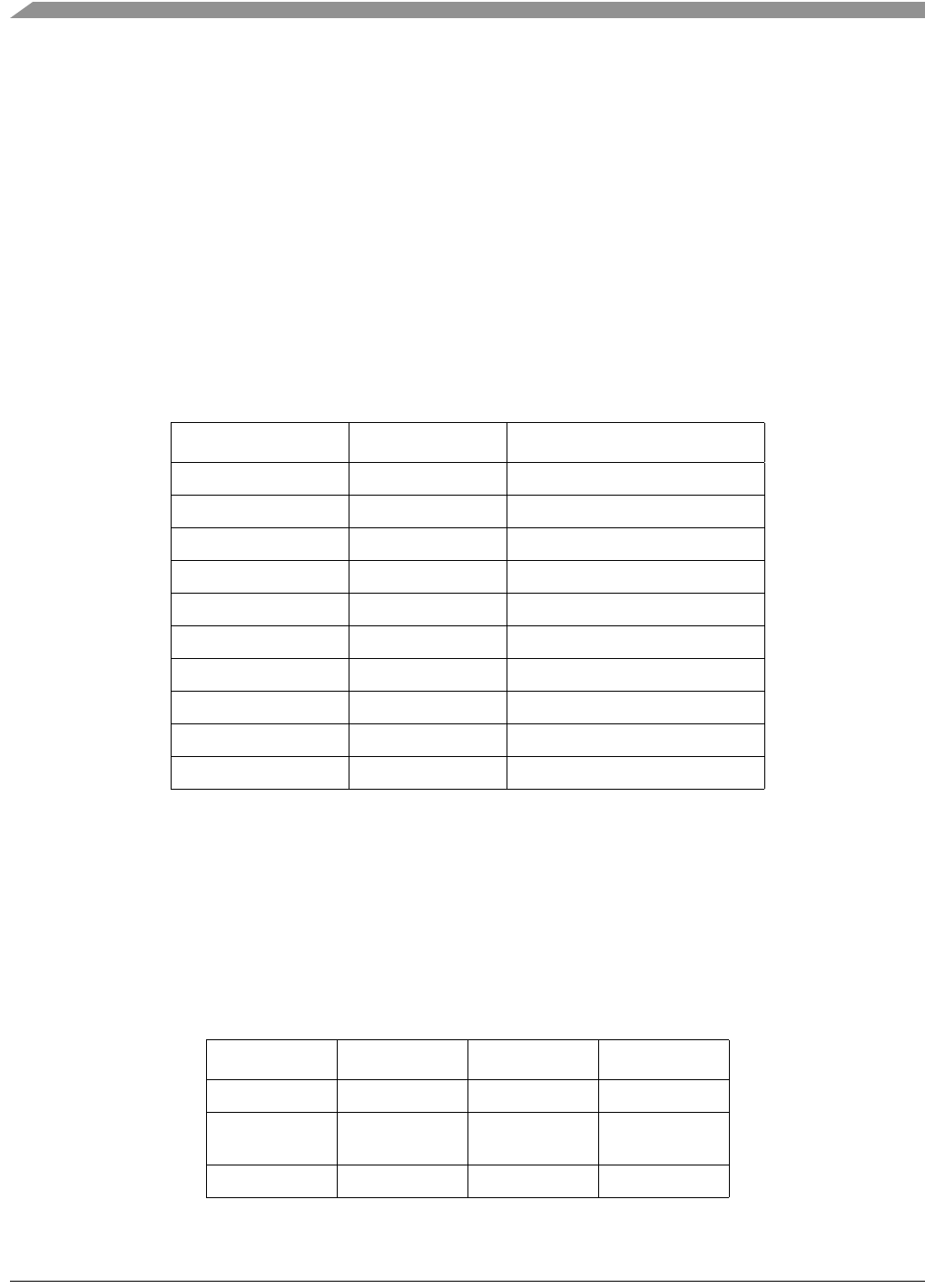
The following table summarizes revisions to this document since the previous release (Rev 0.0).
Revision History
Location Revision
Entire Document First draft of this doc.

1320x-QE128EVB Reference Manual, Rev. 0.0
iv Freescale Semiconductor
Definitions, Acronyms, and Abbreviations
The following list defines the acronyms and abbreviations used in this document.
ADC Analog to Digital Converter
CTS Clear to Send
I2C Inter-Integrated Circuit is a multi-master serial computer bus
ISM Industrial Scientific Medical 2.4 GHz radio frequency band
MAC Media Access Controller
MCU Microcontroller Unit
PCB Printed circuit board
RTS Request to Send
SPI Serial Peripheral Interface
SSI Synchronous Serial Interface
USB Universal Serial Bus

1320x-QE128EVB Reference Manual, Rev. 0.0
Freescale Semiconductor 1-1
Chapter 1
Safety Information
1.1 FCC Guidelines
Any modifications to this product may violate the rules of the Federal Communications Commission and
make operation of the product unlawful.
1.1.1 47 C.F.R. Sec. 15.21
This equipment has been tested and found to comply with the limits for a Class B digital device, pursuant
to part 15 of the FCC Rules. These limits are designed to provide reasonable protection against harmful
interference in a residential installation. This equipment generates, uses and can radiate radio frequency
energy and, if not installed and used in accordance with the instructions, may cause harmful interference
to radio communications. However, there is no guarantee that interference will not occur in a particular
installation. If this equipment does cause harmful interference to radio or television reception, which can
be determined by turning the equipment off and on, the user is encouraged to try to correct the interference
by one or more of the following measures:
• Reorient or relocate the receiving antenna.
• Increase the separation between the equipment and receiver.
• Connect the equipment into an outlet on a circuit different from that to which the receiver is
connected.
• Consult the dealer or an experienced radio/TV technician for help.
1.1.2 47 C.F.R. Sec.15.105(b)
This equipment complies with FCC radiation exposure limits set forth for an uncontrolled environment.
The antenna(s) used for this equipment must be installed to provide a separation distance of at least 8
inches (20cm) from all persons.
This device complies with Part 15 of the FCC Rules. Operation is subject to the following two conditions:
1. This device may not cause harmful interference.
2. This device must accept any interference received, including interference that may cause undesired
operation.
3. This device is susceptible to electrostatic discharge (ESD) and surge phenomenon.

Safety Information
1320x-QE128EVB Reference Manual, Rev. 0.0
1-2 Freescale Semiconductor
1.1.3 47 C.F.R. Sec.15.203
An intentional radiator shall be designed to ensure that no antenna other than that furnished by the
responsible party shall be used with the device. The use of a permanently attached antenna or of an
antenna that uses a unique coupling to the intentional radiator shall be considered sufficient to comply with
the provisions of this Section. The manufacturer may design the unit so that a broken antenna can be
replaced by the user, but the use of a standard antenna jack or electrical connector is prohibited. This
requirement does not apply to carrier current devices or to devices operated under the provisions of
Sections 15.211, 15.213, 15.217, 15.219, or 15.221. Further, this requirement does not apply to intentional
radiators that must be professionally installed, such as perimeter protection systems and some field
disturbance sensors, or to other intentional radiators which, in accordance with Section 15.31(d), must be
measured at the installation site. However, the installer shall be responsible for ensuring that the proper
antenna is employed so that the limits in this Part are not exceeded.
1.2 Disposal Instructions
This product may be subject to special disposal requirements. For product disposal instructions, refer to
www.freescale.com/productdisposal.
1320x-QE128EVB Reference Manual, Rev. 0.0
Freescale Semiconductor 2-1
Chapter 2
1320x-QE128EVB Module Overview and Description
2.1 Introduction
The 1320x-QE128EVB is an evaluation board for developing IEEE® 802.15.4/ZigBee® software and
applications ranging from simple proprietary point-to-point connectivity to complete ZigBee mesh
networking on the QE microcontroller platform. The Freescale QE Microcontroller Family is unique in
that the user can use an 8-bit CPU or a 32-bit CPU in a pin-compatible package and also retain the exact
same peripheral and IO set. The 1320x-QE128EVB uses the MC9S08QE128 Microcontroller unit which
is the first device of the pin-compatible 8-bit and 32-bit duo in the Flexis Series family. The Flexis series
of controllers is the connection point of the Freescale Controller Continuum, delivering 8- and 32-bit
compatibility for migration flexibility.
The 1320x-QE128EVB evaluation board is based on the Freescale MC1320x transceiver and
MC9S08QE128 Microcontroller unit (which is supplied as a daughter card). The 1320x-QE128EVB
provides a platform to evaluate the MC1320x and MC9S08QE128 devices, develop software and
applications, and demonstrate IEEE 802.15.4 and ZigBee networking capabilities. The evaluation board
is supported by Freescale’s BeeKit software design environment for IEEE 802.15.4/ZigBee applications.
Figure 2-1. 1320x-QE128EVB

1320x-QE128EVB Module Overview and Description
1320x-QE128EVB Reference Manual, Rev. 0.0
2-2 Freescale Semiconductor
2.2 Features
The 1320x-QE128EVB provides the following features:
• Uses MC9S08QE128 MCU Daughter card - supports the 9S08 based version of the QE128
• Full IEEE 802.15.4 compliant wireless node; ZigBee capable with Freescale’s BeeStack software
stack
• Based on Freescale’s MC13202 transceiver in RF single-port mode
— Printed F-antenna
— Typical RX sensitivity of -92 dBm at 1.0% Packet Error Rate
— Typical 0 dBm up to 3.6 dBm Maximum Output Power
• Based on Freescale’s MC9S08QE128 Microcontroller Unit
— 50 MHz 8-bit 9S08 CPU core / 25 MHz bus speed
— 128 KB flash memory
— Up to 8 KB RAM
— Single-wire background debug interface
— Device available in 64-pin and 80-pin LQFP packages (evaluation board daughter card uses
80-pin device)
• USB interface is bus-powered and full-speed compatible to the USB 2.0 and 1.1 specifications
• Alternate RS-232/UART (DB-9) serial communication port provided
• User interface switches and LEDs
— 4 pushbuttons for application purposes
— 4 processor controlled red LEDs for application purposes
• Supports a 2x16 Character LCD
• Provides an external 1Mbit serial I2C EEPROM
• Audio Resonator
• Uses standard QE128 BDM Development Port
• Supported by Beekit software development environment
• System clock options
— MCU source derived standard from transceiver CLKO (MC13202 transceiver requires 16 MHz
crystal)
— Optional 32.768 kHz crystal oscillator for accurate real-time delays and low Power Modes
• Power management circuit with on-board regulation for multiple power sources
— Can be powered from USB interface, DC power jack or two AA batteries
— On/Off power switch
— Power-on green LED
• MCU & Transceiver RESET via ON/OFF switch (MCU does not support use of a hardware reset
pin when used with the MC13202 transceiver)
• 16-pin and 10-pin user headers for selected General Purpose Input Output signals (GPIO) and data
interfaces
1320x-QE128EVB Module Overview and Description
1320x-QE128EVB Reference Manual, Rev. 0.0
Freescale Semiconductor 2-3
• All components meet RoHs and WEE requirements
2.3 Board Level Specifications
Table 2-1. MC1320x and QE128 EVB Specifications
Parameter Units Notes/Conditions
MIN TYP MAX
General
Size (PCB: X, Y) 165 x 101 mm
Layer build (PCB) 1.6 /
0.062 mm/in 4-Layer
Dielectric material (PCB) FR4
Power
Voltage supply (DC) 4.4 5 12 V
Voltage supply (USB) 4.4 5 5.25 V USB 2.0/1.1 standard specification
Voltage supply (Batteries) 3 3.2 V
Current consumption 70 mA
Temperature
Operating temperature (see note) -20 +25 +85 °C The operating temperature is limited to +70°C with the
monochrome-graphic LCD module applied
Storage temperature -30 +25 +85 °C
Interfaces
USB interface USB 2.0 and 1.1 full-speed compatible
RS-232 interface DE-9 (TIA-574)
Audio
Buzzer frequency 4 kHz
Sound Pressure Level 83 dB Buzzer Specification
RF
802.15.4 Frequency range 2405 2480 MHz All 16 channels in the 2450 MHz band
Range (outdoor / line of sight) 300 Meter
RF Transmitter
802.15.4 Output power -30 0 +2.5 dBm Over range of Pout from IC control in 2 dB steps
Harmonics
2nd harmonics
3rd harmonics -38
-35 dBc
dBc
Harmonics are compliant to ETSI and FCC regulatory
approval standards
RF Receiver
802.15.4 sensitivity -87 dBm <1% PER
1320x-QE128EVB Module Overview and Description
1320x-QE128EVB Reference Manual, Rev. 0.0
2-4 Freescale Semiconductor
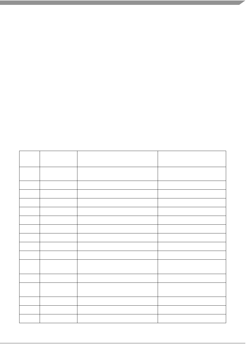
Regulatory Approval
FCC Product is approved accordingly to the FCC part 15
standard
CE (ETSI) Product is approved accordingly to the EN 300 328
V1.7.1 (2006-10) standard
CE (EMC) Product is approved accordingly to the EN 301 489-1
V1.6.1 (2005-09) and EN 301 489-17 V1.2.1 (2002-08)
standards
Safety
UL Product is approved accordingly to the IEC 60950-1 and
EN 60950-1, First Edition standards
Environment
RoHS Product complies with the EU Directive 2002/95/EC of
27 January 2003
WEEE Product complies with the EU Directive 2002/95/EC of
27 January 2003
Table 2-1. MC1320x and QE128 EVB Specifications (continued)
Parameter Units Notes/Conditions
1320x-QE128EVB Reference Manual, Rev. 0.0
Freescale Semiconductor 3-1
Chapter 3
System Overview and Functional Block Descriptions
This section provides a system overview of the 1320x-QE128EVB module and shows block diagrams.
3.1 System Block Diagram
Figure 3-1 shows the 1320x-QE128EVB system level block diagram.
Figure 3-1. MC1320x and QE128 EVB Block Diagram
Power
Management
LT1129CST-3.3
DC ADAPTOR
2XAA BATTERY
USB POWER
Debug Interface
BDM
MCU
QE128
Daughter Board
MC1320X
Transceiver
SPI
CLKO
RS232
Interface
USB
Interface
RS-232
USB 2.0
4 Push
Buttons
1 ON/OFF
switch
4 Red LEDs
1 Green LED
X-TAL 32.768KHz
On-board External Clock X-TAL 16 MHz
EEPROM BUZZER
GPIO
Connectors
Power
Management
LT1129CST-3.3
DC ADAPTORDC ADAPTOR
2XAA BATTERY2XAA BATTERY
USB POWERUSB POWER
Debug Interface
BDM
MCU
QE128
Daughter Board
MC1320X
Transceiver
SPI
CLKO
RS232
Interface
USB
Interface
RS-232
USB 2.0
4 Push
Buttons
1 ON/OFF
switch
4 Red LEDs
1 Green LED
X-TAL 32.768KHz
On-board External Clock X-TAL 16 MHz
EEPROM BUZZER
GPIO
Connectors

System Overview and Functional Block Descriptions
1320x-QE128EVB Reference Manual, Rev. 0.0
3-2 Freescale Semiconductor
3.2 System Overview
The 1320x-QE128EVB combines the Freescale MC1320x Family of IEEE 802.15.4 transceivers to the
9S08 version of QE128 Family of Microcontrollers. The MC9S08QE128 is a natural extension to existing
9S08-based platforms in that it uses the same CPU core, but extends the FLASH memory space to 128
kbytes. The standard 9S08GT/GB maximum FLASH space is 60 kbytes, while the MC9S08QE128
expands the code space to a full 128 kbytes.
The 1320x-QE128EVB provides the MCU as a daughter card and adds the required 802.15.4 transceiver,
RF circuitry, and interface elements.
NOTE
Although the 1320x-QE128EVB provides the MCU as a pre-fabricated
daughter card, the designer must use and reference the MCU by its device
designation (MC9S08QE128, MC9S08QE96, and MC9S08QE64). The
MC9S08QE128 Series Data Sheet (Document number: MC9S08QE128)
and MC9S08QE128 Reference Manual (Document number:
MC9S08QE128RM) are available on the Freescale web site
(www.freescale.com) and links are provided on the Freescale ZigBee/IEEE
802.15.4 page (www.freescale.com/zigbee).
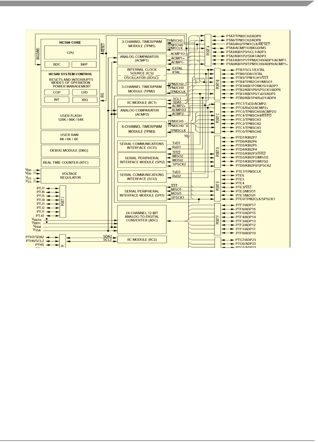
3.2.1 MC9S08QE128 MCU Module
The 1320x-QE128EVB provides the MC9S08QE128 8-bit HCS08 core microcontroller unit via a 64-pin
daughter card, designated as MC9S08QE128_Daughter_card. Figure 3-2 shows the block diagram of the
structure of the MC9S08QE128 Series MCU.
The MC9S08QE128 device provides a 50MHz 9S08 CPU core, 8 Kbytes of RAM, 131 Kbytes of on-board
ROM, and internal clock source. In addition to the CPU core and memory, on-board peripherals include
the following:
• Two dedicated UART modules
• Keyboard interface capability.
• Up to 24 channels of 12-bit analog-to-digital converters (ADCs) with output formatted in 12-, 10-
or 8-bit right-justified channels
• General Purpose I/O available ports.
• Two Inter-integrated Circuit Interface (I2C) modules
• Two Synchronous Peripheral Interface (SPI) modules
• Real Time Clock (RTC) counter
• Two analog comparator (ACMP) modules
System Overview and Functional Block Descriptions
1320x-QE128EVB Reference Manual, Rev. 0.0
Freescale Semiconductor 3-3
Figure 3-2. MC9S08QE128 Series Block Diagram
3.2.2 MC1320x IEEE 802.25.4 Transceiver
The MC1320x family is Freescale’s second generation of ZigBee / IEEE 802.15.4 compliant integrated
circuit transceivers (see Figure 3-3). The MC1320x Family is organized as follows:
• The MC13201 - is a short range, low power, IEEE 802.15.4 2.4 GHz Industrial, Scientific, and
Medical (ISM) band transceiver. The MC13201 contains a complete packet data modem which is
compliant with the IEEE 802.15.4 Standard PHY (Physical) layer. It is a low cost device limited to
custom applications using the 802.15.4 PHY layer, but cannot support a full 802.15.4 MAC
• The MC13202 - is compatible with the MC13201 and extends the IEEE 802.15.4 functionality to
support the complete MAC functionality through a streaming data capability. The MC13202 can
be used with Freescale’s IEEE 802.15.4 MAC and BeeStack, which is Freescale’s
ZigBee-compliant protocol stack.

System Overview and Functional Block Descriptions
1320x-QE128EVB Reference Manual, Rev. 0.0
3-4 Freescale Semiconductor
Figure 3-3. MC1320x Modem Block Diagram
Features of the MC1320x transceiver include:
• Fully compliant IEEE 802.15.4 Standard transceiver supports 250 kbps O-QPSK data on one of
sixteen 5.0 MHz channels and full spread-spectrum encode and decode
• Three power down modes for increased battery life
• Four internal timer comparators available to supplement MCU timer resources
• Supports both Packet Mode and Streaming Mode data transfer
• Buffered transmit and receive data packets
3.2.3 1320x-QE128EVB System Functions
The 1320x-QE128EVB is a self-contained wireless node and development module. The module augments
the basic MCU and transceiver with the following functionality:
• Complete functional, low-cost 2.4 GHz ISM Band IEEE 802.15.4 radio
• 2.0 USB connection
• User interface with pushbuttons, LEDs, and 16 character x 2 line monochromatic LCD
• Versatile power sources and management
• Debug / development port
• GPIO connectors for system expansion
Users are encouraged to reference the board schematic for the topics covered in the following sections.

System Overview and Functional Block Descriptions
1320x-QE128EVB Reference Manual, Rev. 0.0
Freescale Semiconductor 3-5
3.3 Power Management and Measurement
To allow maximum versatility, the 1320x-QE128EVB can be powered via a DC source (typically an
AC-DC converter; nominally 5 Vdc), the USB node, or an on-board battery pack with 2 AA alkaline
batteries.
• The DC source or USB will automatically shutdown the battery supply
• The DC source and the USB power are regulated to 3.3 V, however, the raw battery pack voltage
directly supplies the circuitry
• All sources are isolated via diodes
• An on/off switch and a power-on LED are provided (see Section 4.2.2, “On/Off Switch (Hardware
Reset)”)
• Zero-ohm resistors are provided to allow isolation and measurement of various system components
(see Section 4.2.4, “Power Measurement”)
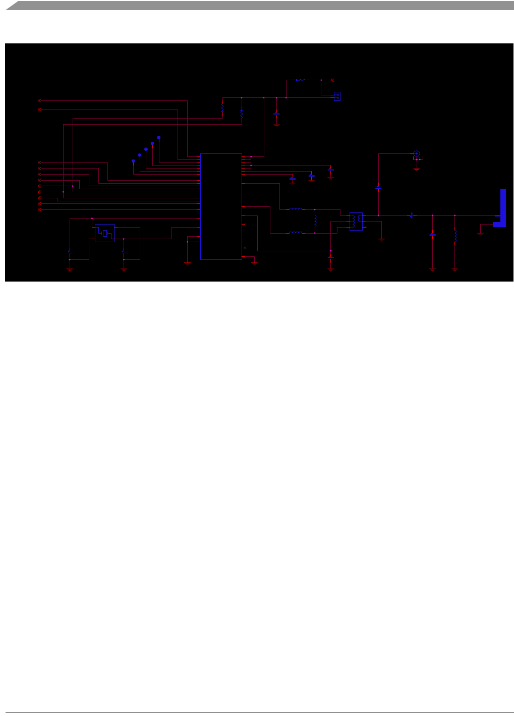
3.4 Low-cost 2.4 GHz IEEE 802.15.4 ISM Band Radio
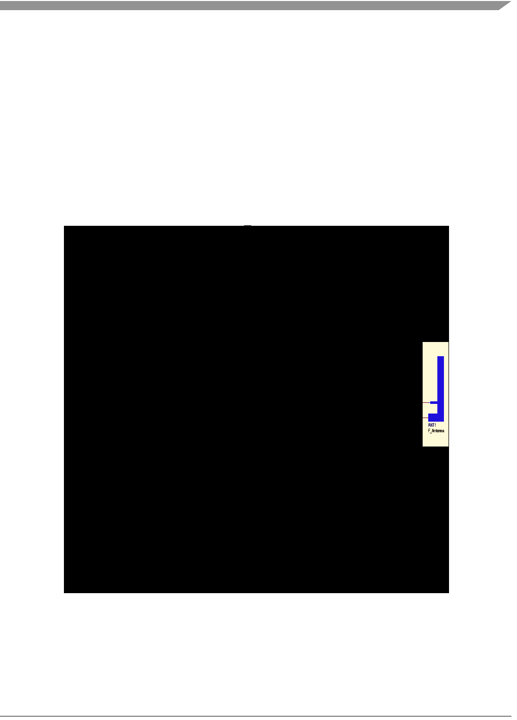
The 1320x-QE128EVB provides a complete RF node which only requires a balun and antenna (external
to the MC1320x). The design uses a PCB printed metal F-antenna for an efficient, low cost solution.
Figure 3-4 shows the RF network external to the MC1320x.
The RF design provides:
• -1 to 0 dBm nominal output power, programmable from -27 dBm to +3 dBm typical
• Receive sensitivity of <-92 dBm (typical) at 1% PER, 20-byte packet, much better than the
802.15.4 Standard of -85 dBm
• Integrated transmit/receive switch
• Typical range (outdoors, line of sight) of 300 meters
• Optional on-board LC filter for harmonic filtering
System Overview and Functional Block Descriptions
1320x-QE128EVB Reference Manual, Rev. 0.0
3-6 Freescale Semiconductor
Figure 3-4. RF Interface Network
3.5 Interfaces
The module provides multiple interfaces for both debug and demonstration.
• USB 2.0 full speed compatible interface
• 16 x 2 monochrome character LCD display
• BDM Debug and Development interface
• Four individual pushbuttons can be used as input and have interrupt generation capability
• Four individual LEDs can be used as indicators for debug or status
• A fully buffered RS232 serial interface with RTS/CTS control is supplied as a secondary COM port
3.5.1 USB Interface
Primary communication with an application device or platform is provided by a USB port with a USB “B”
receptacle plug. USB connectivity is provided by a FTDI FT232R USB < > UART device that appears as
a virtual COM port (VCP) to a connected PC. PC drivers are provided with the module. For pinout
information, see Section , “The 1320x-QE128EVB RF circuitry contains a printed metal F-antenna
(ANT1).”.
The USB interface is configured as a “bus powered” device and can draw all required power from the USB
interface. The device is USB 2.0 full speed compatible.
V_RF
PTC3/GPIO1
PTC4/GPIO2
PTB5/SS1
PTB4/MISO 1
PTB3/MOSI 1
PTB2/SPSCK 1
IRQ
PTC1/ATTN
PTC2/RXTXEN
PTC0/RST
CLKO
V_RF
J1 and R20 for
Current and
Voltage
Measurements
R20
0 OHM
DNP
R20
0 OHM
DNP
ANT1
F_Antenna
ANT1
F_Antenna
U1
MC13202FC
U1
MC13202FC
/ATTN
14
/CE
19
CLKO
15
GPIO1
11
GPIO2
10
GPIO3
9
GPIO4
8
GPIO7
25
GPIO5
23
GPIO6
24
/IRQ
20
MISO
18
MOSI
17
PAO_M 6
PAO_P 5
RIN_M 1
RIN_P 2
/RST
12 RXTXEN
13
SM
7
SPICLK
16
NC 4
CT_Bias 3
XTAL1
26
XTAL2
27
VBATT 31
VDDA 32
VDDD 21
VDDINT 22
VDDLO1 29
VDDLO2 28
VDDVCO 30
EP
33
C3
0.1UF
C3
0.1UF
TP8TP8
C4
0.1UF
C4
0.1UF
L4
3.9nH
DNP
L4
3.9nH
DNP
12
L3
1.8nH
L3
1.8nH
1 2
R1
10K
R1
10K
C6
10PF
C6
10PF
C2
0.1UF
C2
0.1UF
TP9TP9
L1
1.8nH
L1
1.8nH
1 2
CN1
SMA
142-0701-801
DNP
CN1
SMA
142-0701-801
DNP
C10
8PF
C10
8PF
C1
0.1UF
C1
0.1UF
Y1
NX3225SA-16.000000MHZ
Y1
NX3225SA-16.000000MHZ
1 4
32
C9
8PF
C9
8PF
TP10TP10
J1
HDR_2X1
J1
HDR_2X1
1
2
L2
3.9nH
L2
3.9nH
12
C8
10PF
C8
10PF
Z1
LDB212G4005C-001
Z1
LDB212G4005C-001
5
1
6
2
3
4
C5
10PF
DNP
C5
10PF
DNP
R46
470K
R46
470K
TP11TP11
C7
1PF
DNP
C7
1PF
DNP
TP7TP7

System Overview and Functional Block Descriptions
1320x-QE128EVB Reference Manual, Rev. 0.0
Freescale Semiconductor 3-7
3.5.2 16x2 Monochrome Character LCD Display
The 1320x-QE128EVB supports a 16x2 monochrome character LCD that provides for alpha-numeric
readout. The LCD module is mounted on top of the main circuit board and connects via a 16 pin header
with 0.1in spacing. For pinout information, see Section 4.6, “LCD Connector”.
• The module supports two similar LCD modules, one of which is the CFAH1602NYG-JP STN
daughter board from Crystalfontz.
• The LCD operates from 5 Vdc generated from the main operating voltage. The LCD module
requires a highly regulated 5V so that the high voltages generated on-board the display are
consistent.
• The LCD uses no backlighting
• LCD interface to the MCU is via an 4-bit parallel interface
• The on-board controller is a industry-standard HD44780 compatible controller
3.5.3 Debug/Development Interface
The 1320x-QE128EVB contains a standard BDM debug port. For pinout information see Section 4.8,
“Debug/Development Connector (BDM Interface)”). A 6-pin connector is provided for the standard BDM
debug interface.
3.5.4 RS232 Interface
The 1320x-QE128EVB provides a secondary standard RS232-compatible UART serial port with the
connection provided by a standard DB9 connector (J14). For pinout information see Section 4.9,
“RS232-Compatible UART Connector”.
3.6 GPIO Connectors
Two GPIO connectors (J3 and J4) provide connection to data interfaces and GPIO for external system
expansion of the MCU resources. For pinout information see Section 4.10, “GPIO Connectors”.
• Some GPIO are shared with on-board devices. The user should be careful to avoid conflict.
• External current draw should be limited to 50 mA maximum.

System Overview and Functional Block Descriptions
1320x-QE128EVB Reference Manual, Rev. 0.0
3-8 Freescale Semiconductor
3.7 Clocks
The primary clock source for the 1320x-QE128EVB is supplied by the MC1320x transceiver. The
transceiver requires an accurate 16 MHz reference clock that is supplied via an on-board 16 MHz crystal
oscillator, and in turn, the transceiver typically supplies the clock for the MCU. However, there are options
for the MCU clock usage:
• The default clock source for the QE128 is obtained through MC1320x CLKO programmable
frequency clock output. The RF transceiver reference oscillator is 16 MHz and the mounted crystal
Y1 is a 16 MHz device that meets MC1320x specifications. In turn, CLKO can be enabled to
provide the clock source to the MCU as an external input.
• The QE128 Internal Clock Source (ICS) supplies an optional on-board reference oscillator (32KHz
nominal). With use of the on-board Frequency-locked-loop (FLL), CPU frequencies from 2-50
MHz are available. Precision trimming of the internal reference allows for 0.2% resolution and 2%
deviation over temperature and voltage.
• The module also supports optional use of an external 32.768KHz crystal for the MCU. The
on-board MCU clock amp is used with the 32KHz crystal, and higher CPU and bus clock
frequencies are again synthesized through use of the on-board FLL in the ICS.
The external source of clock is selected by Jumper (J5) (See Section 4.11, “Jumper Selection”).
1320x-QE128EVB Reference Manual, Rev. 0.0
Freescale Semiconductor 4-1
Chapter 4
Interface Locations and Pinouts
This chapter provides a description of the interface locations and pinouts of the 1320x-QE128EVB printed
circuit board.
4.1 Overview
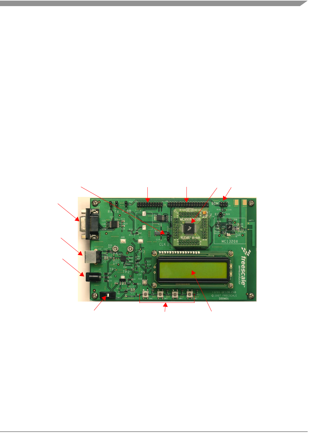
This section details the locations (as shown in Figure 4-1) and descriptions of switches, jumpers, and
connectors on the 1320x-QE128EVB main circuit board. The MC9S08QE128 MCU module and the LCD
module mount on the main board as daughter cards. Users should refer to the figures in the subsequent
sections while moving through this chapter. Users should also reference the main circuit board schematic
in Section 5.1, “Schematic” , for additional information.
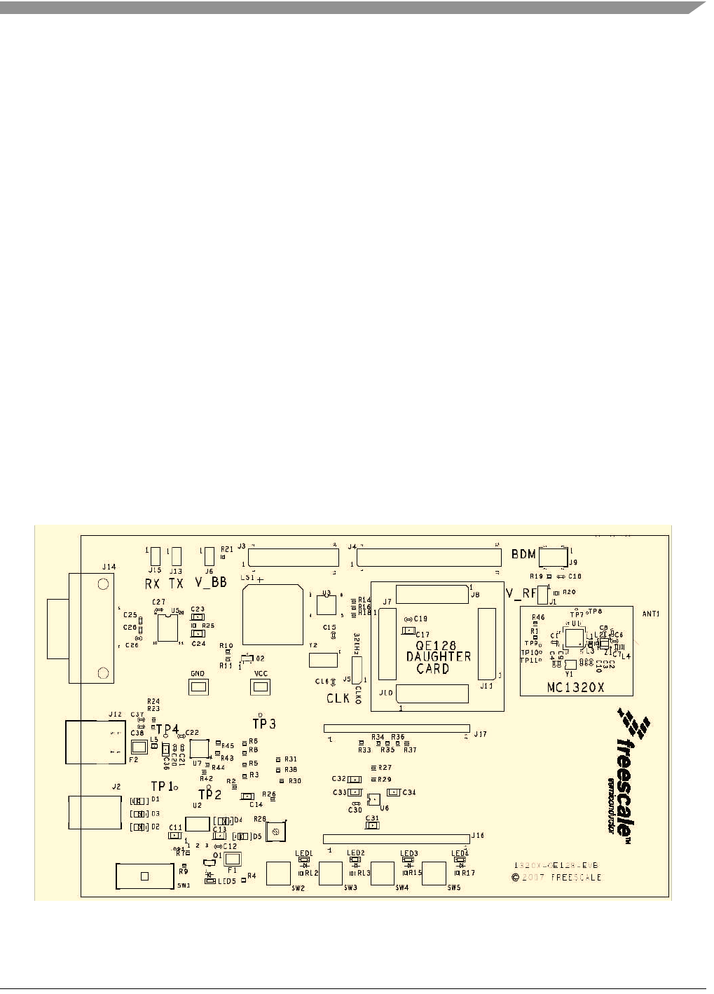
Figure 4-1. The 1320x-QE128 PCB Top View
LCD
CLK GPIO J3 GPIO J4 MCU BDM
SW2-SW5
RS-232
USB
DC Supply
SW1 (On-Off)

Interface Locations and Pinouts
1320x-QE128EVB Reference Manual, Rev. 0.0
4-2 Freescale Semiconductor
4.2 Power Management
The module can be powered from the DC power jack, the USB port, or the battery pack.
4.2.1 Supply Sources
Table 4-1 lists the supply sources, connectors, and voltages. Maximum board current draw is rated at 100
mA.
4.2.2 On/Off Switch (Hardware Reset)
The slide switch designated SW1 provides an on/off function and the only hardware reset to the main board
and subsystems.
• The hardware reset was implemented through power on/off because of the IO/reset configuration
of the MC9S08QE128 MCU. The MCU has a single pin that can be used as an external interrupt
request (IRQ) or hardware reset input. In this application the MC1320x transceiver requires use of
the external IRQ function, and as a result, the MCU cannot directly use the hardware reset pin. For
the module, the only hardware reset is to cycle main power through SW1.
• When the module is powered from the USB connection, the USB interface IC is always powered
and SW1 does not disconnect power from it. This has been done such that switching power via
SW1 does not disrupt connection with a PC and cause software driver problems with the
applications software.
4.2.3 Power On Indicator
Green light emitting diode LED5 is the power on indicator for any source. The LED is active anytime a
power source is present and SW1 is ON. If the power source is the USB connection, LED5 will be inactive
when SW1 is open (off), but the USB interface device will be powered as long as connected to the USB
bus.
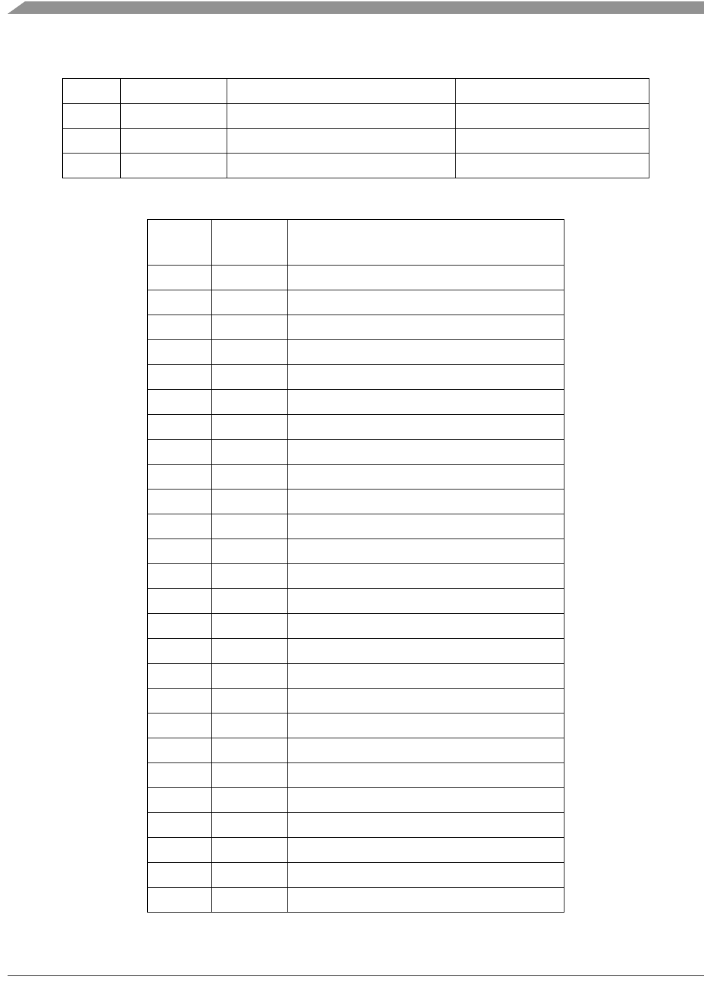
Table 4-1. Power Supply Sources
Source Connector Min
(Volts) Typical
(Volts) Max
(Volts) Notes
DC Source J2 4.4 5 12 Use DC only source. The connector is a 2 mm DC power jack;
positive center conductor.
USB J12 4.4 5 5.25 Per USB specification. Power from USB connector.
AA Battery Pack BT1 ~2.0 3 3.2 Two AA cells. Battery pack is automatically disabled by either
DC source or USB.
Interface Locations and Pinouts
1320x-QE128EVB Reference Manual, Rev. 0.0
Freescale Semiconductor 4-3
4.2.4 Power Measurement
It is possible to isolate various circuit blocks to measure current draw via 0-ohm resistors. The resistors
are all mounted as default.
Below is a list of the supply nodes.
• R8 -> V_RS232 (Supply for RS-232 Transceiver circuit)
• R6 -> V_PERIF (Output from on-board regulator for GPIO customer access)
• R5 -> V_LCD (Supply for LCD Daughter Board)
• R21 -> V_BB (Supply for QE128 EVB)
• R20 -> V_RF (Supply for MC1320x)
• R3 -> V_LED (Supply for LEDs)
• R2 -> VCC (Output from main on-board regulator)
4.3 MC9S08QE128 MCU Module
The MC9S08QE128 MCU is provided as a module that mounts as a daughter card on the main PBC. Four
2x8 headers designated J7, J8, J10, and J11 are used to mount the module.
NOTE
The MCU is mounted to the module during manufacturing. Freescale
recommends that users do not remove and replace this module.
4.4 RF Circuitry
The 1320x-QE128EVB RF circuitry contains a printed metal F-antenna (ANT1).
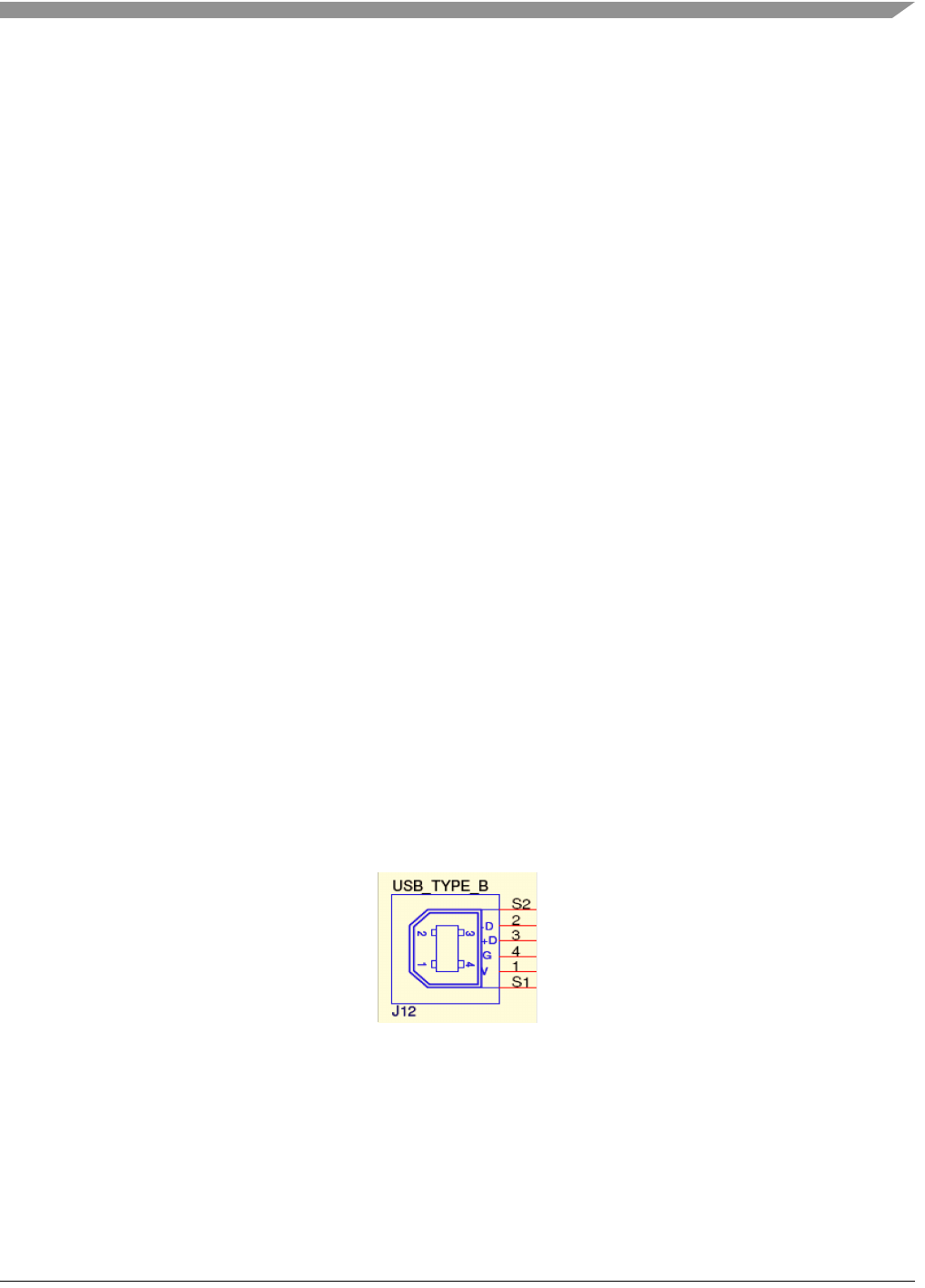
4.5 USB Connector (“B” Receptacle)
The USB connector is a “B”-type device and is designated as J12. Figure 4-2 shows the connector pinout.
The USB port is connected to MCU port SCI2.
Figure 4-2. USB Connector Pinout
4.6 LCD Connector
The LCD module is connected to the main circuit board via one of two 16-pin connectors (either J16 or
J17). Each connector supports a different LCD module format. The default LCD designated as the
CFAH1602B device uses the J17 connector.
Interface Locations and Pinouts
1320x-QE128EVB Reference Manual, Rev. 0.0
4-4 Freescale Semiconductor
4.7 LEDs and Switches
The 1321x-QE128EVB contains four red LEDs and one green LED
• The four red LEDs (LED1 through LED4) are intended to be application-based indicators and are
driven by the MCU and controlled by the software application.
• As already stated, the green LED is directly connected to the on-board main supply and acts as the
“Power On” indication.
There is a slide switch and 4 pushbuttons.
• SW1 is an on/off slide switch that connects the power supplies.
• Four additional pushbuttons (SW2 through SW5) are connected to the MCU GPIO and are
intended as application input devices. All four buttons have interrupt generation capability.
4.8 Debug/Development Connector (BDM Interface)
The 1320x-QE128EVB supports connection to a subset of the defined BDM connector. The BDM
interface is a standard 2.54mm/0.1inch spacing, 6-pin debug interface (J9). The 6-pin connector is clearly
separated from the GPIO pin headers (J3, J4) and located at the upper right corner of top side of the
module. The 6-pin connector has Pin 1 marking for correct plug-in of the development cable.
Table 4-3 shows the BDM header pinout.
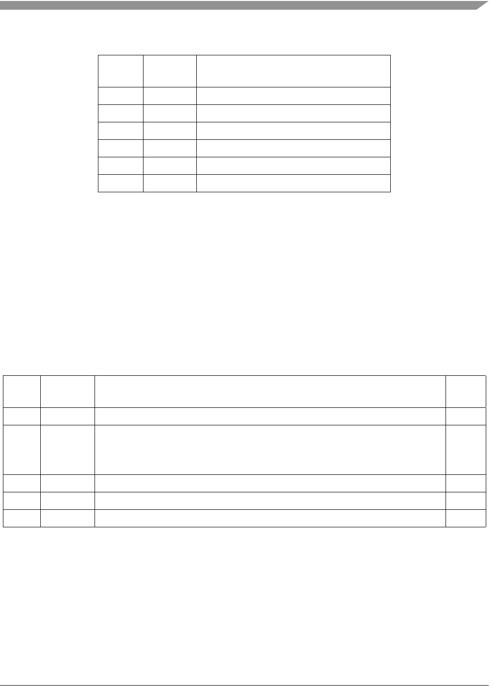
Table 4-2. Switch and LED Summary
Item GPIO Connection Feature
PWR LED (green) VCC ‘Power On’ indication
LED1 (red) PTE3 Application specific
LED2 (red) PTE4 Application specific
LED3 (red) PTE5 Application specific
LED4 (red) PTE6 Application specific
SW2 (pushbutton) PTD0 Interrupt functionality.
SW3 (pushbutton) PTD1 Interrupt functionality.
SW4(pushbutton) PTD2 Interrupt functionality.
SW5 (pushbutton) PTD3 Interrupt functionality.
SW1 (ON/OFF) ON/OFF HW ON/OFF
Table 4-3. BDM 6-Pin Connector Assignments (J9)
Name Pin # Pin # Name
BKGD 1 2 GND
NC13 4 Pullup2
(RESET)
NC 5 6 V_BB
Interface Locations and Pinouts
1320x-QE128EVB Reference Manual, Rev. 0.0
Freescale Semiconductor 4-5
4.9 RS232-Compatible UART Connector
The 1320x-QE128EVB provides a secondary standard RS232-compatible UART serial port. Connection
is provided by a standard DB9 connector (J14). The RS232 converter is connected to MCU port SCI1.
4.10 GPIO Connectors
The 1320x-QE128EVB contains two GPIO connectors (J3) and (J4). The GPIO connectors are a standard
2.54mm/0.1inch spacing, 20- and 32-pin header, respectively.
These connectors provide access to MCU GPIO, Timer outputs, ADC inputs, the SPI port, the I2C port,
among others. Power is also provided on both connectors.
• V_PERIF is the main supply voltage. Current draw should be limited to 50 mA.
• Some of the GPIO are shared with on-board devices. Check for any conflict.
1NC = No Connect.
2Pulled-up to V_BB through 51kohms. Hardware reset not supported on
this BDM port.
Table 4-4. GPIO Connector J3 Pinouts
Pin
Number Name Function Notes
1 PTE2/BUZZER GPIO Hardwired to Q2 Base to Turn
On/Off on-board Buzzer (LS1)
2 GND System ground
3 PTF2 ADC Analog Input Channel or GPIO
4 GND System ground
5 PTF3 ADC Analog Input Channel or GPIO
6 GND System ground
7 PTD2 KBI input or GPIO Hardwired to Push Button SW4
8 GND System ground
9 PTD3 KBI input or GPIO Hardwired to Push Button SW5
10 GND System ground
11 PTB0/RxD1 KBI Input or SCI1 or ADC Analog Input
Channel or GPIO Hardwired to J13 and to RS-232
Transceiver
12 GND System ground
13 PTB1/TxD1 KBI Input or SCI1 or ADC Analog Input
Channel or GPIO Hardwired to J15 and to RS-232
Transceiver
14 GND System ground
15 V_PERIF System Supply
16 GND System ground
Interface Locations and Pinouts
1320x-QE128EVB Reference Manual, Rev. 0.0
4-6 Freescale Semiconductor
17 PTH7 I2C Port or GPIO
18 GND System ground
19 PTH6 I2C Port or GPIO
20 GND System ground
Table 4-5. GPIO Connector J4 Pinouts
Pin
Number Name Function
1 V_PERIF System Supply
2 GND System ground
3NC
4 GND System ground
5 PTE7 Timer/PWM Channel or GPIO
6 GND System ground
7PTH1 GPIO
8 GND System ground
9PTH0 GPIO
10 GND System ground
11 PTF1 ADC Analog Input Channel or GPIO
12 GND System ground
13 PTF0 ADC Analog Input Channel or GPIO
14 GND System ground
15 PTD4 KBI input or GPIO
16 GND System ground
17 PTG3 ADC Analog Input Channel or GPIO
18 GND System ground
19 PTG2 ADC Analog Input Channel or GPIO
20 GND System ground
21 PTG1 GPIO
22 GND System ground
23 PTG0 GPIO
24 GND System ground
25 PTE1 SPI Serial Peripheral Interface MOSI or GPIO
26 GND System ground
Table 4-4. GPIO Connector J3 Pinouts (continued)
Interface Locations and Pinouts
1320x-QE128EVB Reference Manual, Rev. 0.0
Freescale Semiconductor 4-7
4.11 Jumper Selection
Table 4-6 lists all the possible jumper selections for the 1320x-QE128EVB. The jumpers available on the
board include:
• J1 - used to measure current and voltage on V_RF
• J5 - used to select clock input to the MCU either from the MC1320x CLKO output or from an
optional on-board (Y2) 32.768KHz crystal.
• J6 - used to measure current and voltage on V_BB
• J13 - used to connect MCU TxD1 pin to the on-board RS-232 transceiver (U5)
• J15 - used to connect MCU RxD1 pin to the on-board RS-232 transceiver (U5)
27 PTE0 Timer/PWM Channel or GPIO
28 GND System ground
29 NC
30 GND System ground
31 NC
32 GND System ground
Table 4-6. Jumper Selection
Jumper Pin Number
Connection Description Default
Setting
J1 1-2 Provide the means for voltage and current measurements on the MC1320x Transceiver Mounted
J5 1-2
2-3
Connects MCU QE128 XTAL with MC1320x CLKO output
Connects MCU QE128 XTAL with on-board 32.768KHz crystal
Mounted
Not
Mounted
J6 1-2 Provide the means for voltage and current measurements on the MCU QE128 Mounted
J13 1-2 Provide the means to connect the on-board RS-232 transceiver with MCU TXD1 Mounted
J15 1-2 Provide the means to connect the on-board RS-232 Transceiver with MCU RXD1 Mounted
Table 4-5. GPIO Connector J4 Pinouts (continued)
Pin
Number Name Function

Interface Locations and Pinouts
1320x-QE128EVB Reference Manual, Rev. 0.0
4-8 Freescale Semiconductor
1320x-QE128EVB Reference Manual, Rev. 0.0
Freescale Semiconductor 5-1
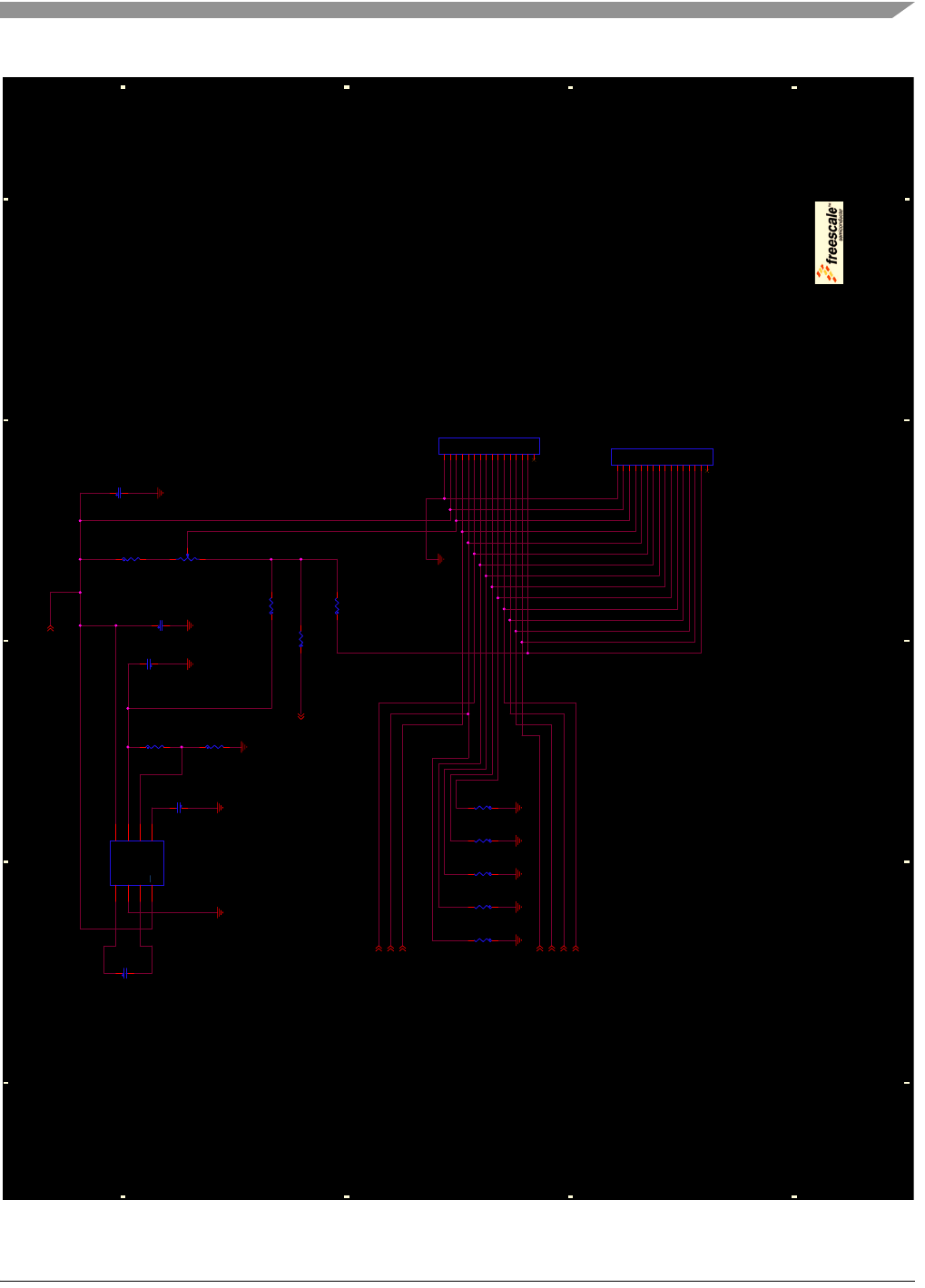
Chapter 5
Schematic and Bill of Material
5.1 Schematic
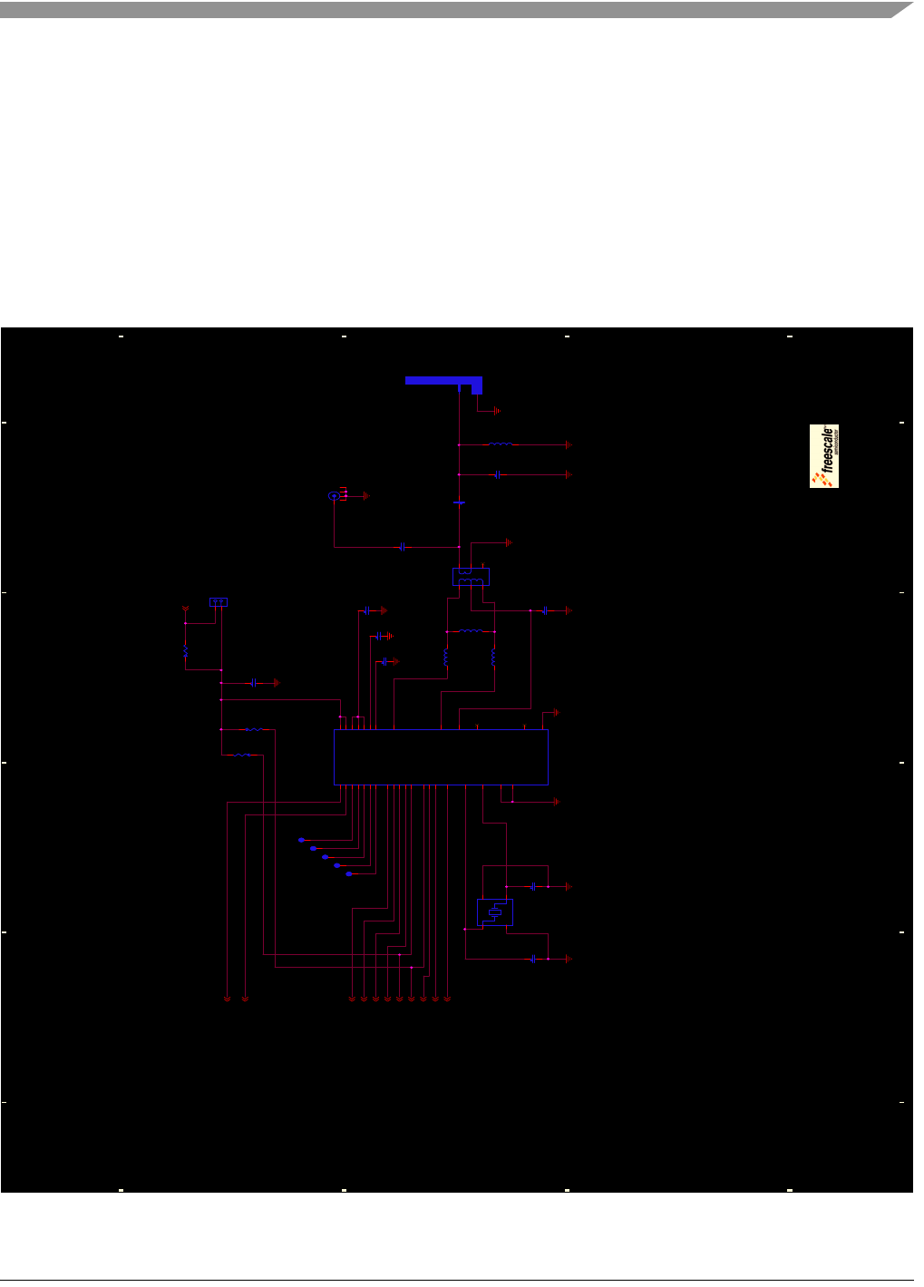
Figure 5-1. Schematic (1 of 5)
5
5
4
4
3
3
2
2
1
1
D D
C C
B B
A A
V_RF
PTC3/GPIO1
PTC4/GPIO2
PTB5/SS1
PTB4/MISO 1
PTB3/MOSI 1
PTB2/SPSCK 1
IRQ
PTC1/ATTN
PTC2/RXTXEN
PTC0/RST
CLKO
Drawing Title:
Size Document Number Rev
Date: Sheet of
Page Title:
SCH-23731 PDF: SPF-23731 B1
1320X-QE128-EVB
C
Friday, February 01, 2008
13202-RF
37
Drawing Title:
Size Document Number Rev
Date: Sheet of
Page Title:
SCH-23731 PDF: SPF-23731 B1
1320X-QE128-EVB
C
Friday, February 01, 2008
13202-RF
37
Drawing Title:
Size Document Number Rev
Date: Sheet of
Page Title:
SCH-23731 PDF: SPF-23731 B1
1320X-QE128-EVB
C
Friday, February 01, 2008
13202-RF
37
V_RF
J1 and R20 for
Current and
Voltage
Measurements
R20
0 OHM
DNP
R20
0 OHM
DNP
ANT1
F_Antenna
ANT1
F_Antenna
U1
MC13202FC
U1
MC13202FC
/ATTN
14
/CE
19
CLKO
15
GPIO1
11
GPIO2
10
GPIO3
9
GPIO4
8
GPIO7
25
GPIO5
23
GPIO6
24
/IRQ
20
MISO
18
MOSI
17
PAO_M 6
PAO_P 5
RIN_M 1
RIN_P 2
/RST
12 RXTXEN
13
SM
7
SPICLK
16
NC 4
CT_Bias 3
XTAL1
26
XTAL2
27
VBATT 31
VDDA 32
VDDD 21
VDDINT 22
VDDLO1 29
VDDLO2 28
VDDVCO 30
EP
33
C3
0.1UF
C3
0.1UF
TP8TP8
C4
0.1UF
C4
0.1UF
L4
3.9nH
DNP
L4
3.9nH
DNP
12
L3
1.8nH
L3
1.8nH
1 2
R1
10K
R1
10K
C6
10PF
C6
10PF
C2
0.1UF
C2
0.1UF
TP9TP9
L1
1.8nH
L1
1.8nH
1 2
CN1
SMA
142-0701-801
DNP
CN1
SMA
142-0701-801
DNP
C10
8PF
C10
8PF
C1
0.1UF
C1
0.1UF
Y1
NX3225SA-16.000000MHZ
Y1
NX3225SA-16.000000MHZ
1 4
32
C9
8PF
C9
8PF
TP10TP10
J1
HDR_2X1
J1
HDR_2X1
1
2
L2
3.9nH
L2
3.9nH
12
C8
10PF
C8
10PF
Z1
LDB212G4005C-001
Z1
LDB212G4005C-001
5
1
6
2
3
4
C5
10PF
DNP
C5
10PF
DNP
R46
470K
R46
470K
TP11TP11
C7
1PF
DNP
C7
1PF
DNP
TP7TP7
Schematic and Bill of Material
1320x-QE128EVB Reference Manual, Rev. 0.0
5-2 Freescale Semiconductor
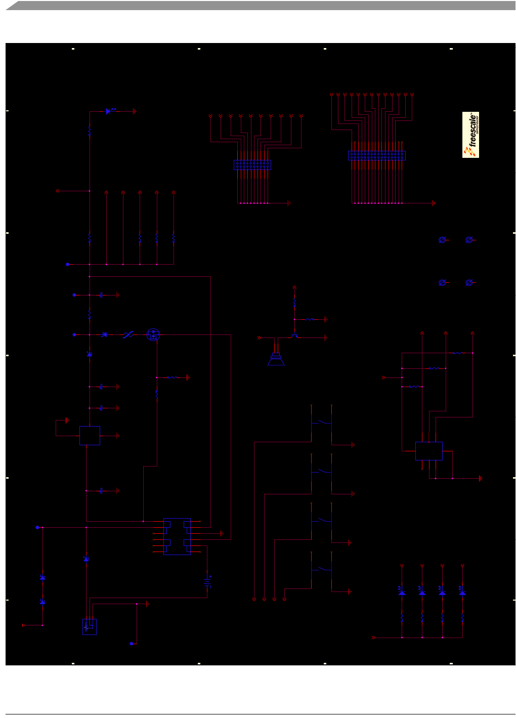
Figure 5-2. Schematic (2 of 5)
5
5
4
4
3
3
2
2
1
1
D D
C C
B B
A A
V_USB
V_RF
V_BB
V_LCD
V_PERIF
V_LED
V_RS232
PTD3
PTD2
PTD1
PTD0
V_LED
PTE3
PTE4
PTE5
PTE6
V_PERIF
PTC5/WC
PTA3/SCL
PTA2/SDA
V_PERIF
PTE2/BUZZER
PTE2/BUZZER
PTF2
PTF3
PTD2
PTD3
PTB0/RxD1
PTB1/TxD1
V_PERIF
PTH7
PTH6
PTE7
PTH1
PTH0
PTF1
PTF0
PTD4
PTG3
PTG2
PTG1
PTG0
PTE1
PTE0
V_PERIF
Drawing Title:
Size Document Number Rev
Date: Sheet of
Page Title:
SCH-23731 PDF: SPF-23731 B1
1320X-QE128-EVB
C
Friday, February 01, 2008
Power & I/O
47
Drawing Title:
Size Document Number Rev
Date: Sheet of
Page Title:
SCH-23731 PDF: SPF-23731 B1
1320X-QE128-EVB
C
Friday, February 01, 2008
Power & I/O
47
Drawing Title:
Size Document Number Rev
Date: Sheet of
Page Title:
SCH-23731 PDF: SPF-23731 B1
1320X-QE128-EVB
C
Friday, February 01, 2008
Power & I/O
47
Test Loop for VCC
Test Loop for
GND
BH3
MOUNTING HOLE
BH3
MOUNTING HOLE
LED2
LED RED
LED2
LED RED
2 1
Q1
ZXM61P02F
Q1
ZXM61P02F
1
32
R9
100K
R9
100K
SW5SW5
A
BB1
A1
J2
DC_POWER_JACK
J2
DC_POWER_JACK
1
2
3
R7
10K
R7
10K
TP5TP5
R15
390 OHMS
R15
390 OHMS
R4
390 OHMS
R4
390 OHMS
SW4SW4
A
BB1
A1
U2
3.3V
U2
3.3V
GND
2
OUTPUT 3
VIN
1TAB
4
LED1
LED RED
LED1
LED RED
2 1
Q2
MMBT3904LT1G
Q2
MMBT3904LT1G
2 3
1
R6
0 OHM
R6
0 OHM
SW3SW3
A
BB1
A1
LED5
LED_GRN_DL
LED5
LED_GRN_DL
21
J4
HDR_2X16
J4
HDR_2X16
12
34
6 5
78
910
1112
1314
1516
1718
1920
2122
2324
2526
2728
2930
3132
BH2
MOUNTING HOLE
BH2
MOUNTING HOLE
D3
MBR0520LT1G
D3
MBR0520LT1G
R14
100K
R14
100K
SW2SW2
A
BB1
A1
R2
0 OHM
R2
0 OHM
TP6TP6
D1
MBR0520LT1G
D1
MBR0520LT1G
R13
390 OHMS
R13
390 OHMS
R8
0 OHM
R8
0 OHM
LED4
LED RED
LED4
LED RED
2 1
C12
0.1UF
C12
0.1UF
D2
MBR0520LT1G
D2
MBR0520LT1G
R16
4.7K
R16
4.7K
POS 1
POS 2
POS 3
POS 4
SW1
4PDT
POS 1
POS 2
POS 3
POS 4
SW1
4PDT
1
2
3
4
5
6
12
11
10
9
8
7
BT1
BATTERY HOLDER
BT1
BATTERY HOLDER
12
R5
0 OHM
R5
0 OHM
R10
1.5K
R10
1.5K
BH1
MOUNTING HOLE
BH1
MOUNTING HOLE
TP2TP2
R12
390 OHMS
R12
390 OHMS
C11
1.0UF
C11
1.0UF
J3
HDR_10X2
J3
HDR_10X2
12
34
6 5
78
910
1112
1314
1516
1718
1920
TP3TP3
LED3
LED RED
LED3
LED RED
2 1
D4
MBR0520LT1G
D4
MBR0520LT1G
+
LS1
BUZZER
+
LS1
BUZZER
1
2
BH4
MOUNTING HOLE
BH4
MOUNTING HOLE
R3
0 OHM
R3
0 OHM
U3
AT24C1024BW
U3
AT24C1024BW
NC
1
A1
2
A2
3
GND
4
WP 7
SDA 5
SCL 6
VCC
8
C14
10UF
C14
10UF
F1
0.5A
F1
0.5A
12
D5
MBR0520LT1G
D5
MBR0520LT1G
C13
10UF
C13
10UF
R18
4.7K
R18
4.7K
TP1TP1
R17
390 OHMS
R17
390 OHMS
R11
10K
R11
10K
Schematic and Bill of Material
1320x-QE128EVB Reference Manual, Rev. 0.0
Freescale Semiconductor 5-3
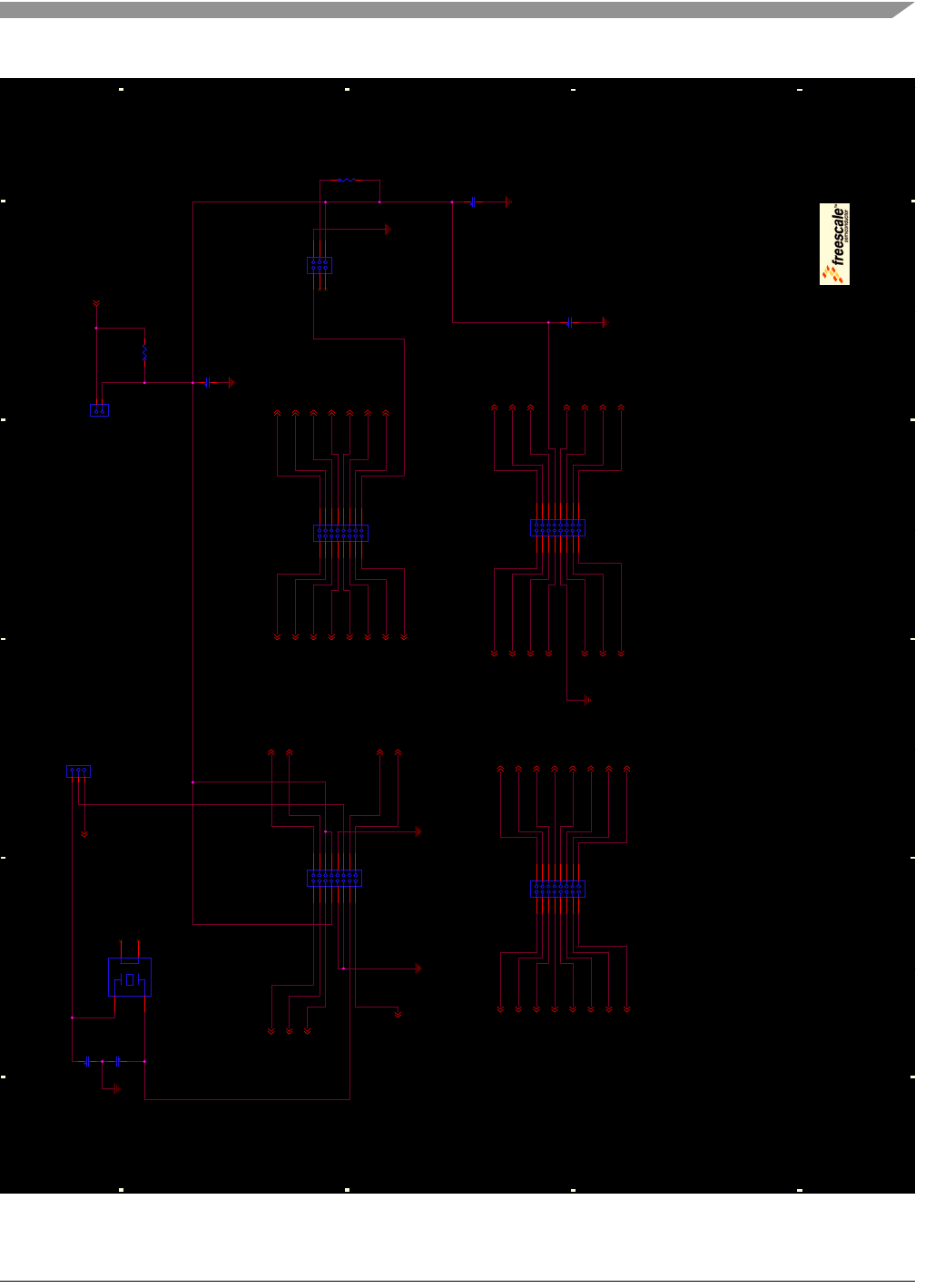
Figure 5-3. Schematic (3 of 5)
5
5
4
4
3
3
2
2
1
1
D D
C C
B B
A A
PTD1
PTH7
PTE7
PTH0
PTE5
PTB4/MISO 1
PTC2/RXTXEN
PTD6
PTC1/ATTN
PTF7
PTF5
PTB3/MOSI 1
PTA1
PTC7/TxD2
PTE3
PTG3
PTG1
PTE1
PTC5/WC
IRQ
PTD0
PTH6
CLKO
PTH1
PTE6
PTB5/SS1
PTC3/GPIO1
PTD7
PTD5
PTC0/RST
PTF6
PTF4
PTB2/SPSCK 1
PTA0
PTC6/RxD2
PTE2/BUZZER
PTG2
PTG0
PTE0
PTC4/GPIO2
PTB1/TxD1
PTF3
PTA7
PTE4
PTF0
PTD3
PTA3/SCL
PTB0/RxD1
PTF2
PTA6
PTF1
PTD4
PTD2
PTA2/SDA
V_BB
Drawing Title:
Size Document Number Rev
Date: Sheet of
Page Title:
SCH-23731 PDF: SPF-23731 B1
1320X-QE128-EVB
C
Monday, November 12, 2007
MCU
57
Drawing Title:
Size Document Number Rev
Date: Sheet of
Page Title:
SCH-23731 PDF: SPF-23731 B1
1320X-QE128-EVB
C
Monday, November 12, 2007
MCU
57
Drawing Title:
Size Document Number Rev
Date: Sheet of
Page Title:
SCH-23731 PDF: SPF-23731 B1
1320X-QE128-EVB
C
Monday, November 12, 2007
MCU
57
WEST NORTH
SOUTH
J5 Pins 1 and 2 --> XCVR CLK OUTPUT
J5 Pins 2 and 3 --> 32kHz
EAST
BDM
V_BB
CLOCK
J6 and R21 for
Current and Voltage
Measurements
R19
51K
R19
51K
J10
HDR_2X8
J10
HDR_2X8
1 2
3 4
65
7 8
910
11 12
13 14
15 16
J11
HDR_2X8
J11
HDR_2X8
1 2
3 4
65
7 8
910
11 12
13 14
15 16
J9
HDR_2X3
J9
HDR_2X3
1 2
3 4
65
J6
HDR_2X1
J6
HDR_2X1
1
2
R21
0 OHM
DNP
R21
0 OHM
DNP
J5
HDR_1X3
J5
HDR_1X3
1
2
3
C15
22PF
C15
22PF
C17
10UF
C17
10UF
C19
0.1UF
C19
0.1UF
J7
HDR_2X8
J7
HDR_2X8
1 2
3 4
65
7 8
910
11 12
13 14
15 16
J8
HDR_2X8
J8
HDR_2X8
1 2
3 4
65
7 8
910
11 12
13 14
15 16
C18
0.1UF
C18
0.1UF
C16
22PF
C16
22PF
Y2
32.768KHZ
Y2
32.768KHZ
1
4
2
3
Schematic and Bill of Material
1320x-QE128EVB Reference Manual, Rev. 0.0
5-4 Freescale Semiconductor
Figure 5-4. Schematic (4 of 5)
5
5
4
4
3
3
2
2
1
1
D D
C C
B B
A A
MCU RXD1
TX
CTS
RTS
RX
MCU TXD1
V_USB
PTC6/RxD2
PTC7/TxD2
PTA7
PTA6
LCD_Vo_ref
V_RS232
PTB1/TxD1
PTB0/RxD1
PTA0
PTA1
Drawing Title:
Size Document Number Rev
Date: Sheet of
Page Title:
SCH-23731 PDF: SPF-23731 B1
1320X-QE128-EVB
C
Friday, February 01, 2008
USB & RS232
67
Drawing Title:
Size Document Number Rev
Date: Sheet of
Page Title:
SCH-23731 PDF: SPF-23731 B1
1320X-QE128-EVB
C
Friday, February 01, 2008
USB & RS232
67
Drawing Title:
Size Document Number Rev
Date: Sheet of
Page Title:
SCH-23731 PDF: SPF-23731 B1
1320X-QE128-EVB
C
Friday, February 01, 2008
USB & RS232
67
TX UART 1
RX UART 1
RS232 Switching Noise Trap
U5
MAX3318EAP
U5
MAX3318EAP
C1+ 2
V+
3C1- 4
C2+ 5
C2- 6
V-
7
T2OUT
8
R2IN
9
R2OUT 10
T2IN 12
T1IN 13
R1OUT 15
R1IN
16
FORCEON 14
INVALID
11
READY
1
VCC
19
FORCEOFF 20
T1OUT
17
GND 18
C37
15 PF
C37
15 PF
R43 1K
R43 1K
R45 1K
R45 1K
C36
4.7UF
C36
4.7UF
C26
0.1UF
C26
0.1UF
C20
0.01UF
C20
0.01UF
C24
4.7UF
C24
4.7UF
1
2
34
+D
-D
G
V
J12
USB_TYPE_B
1
2
34
+D
-D
G
V
J12
USB_TYPE_B
1
2
3
4
S1
S2
J15
HDR_2X1
J15
HDR_2X1
1
2
R23 0 OHMR23 0 OHM
L5
47 OHM
L5
47 OHM
1 2
R42 1K
R42 1K
R44 1K
R44 1K
R25
10 OHM
R25
10 OHM
J14
DB9
J14
DB9
5
9
4
8
3
7
2
6
1
M2
M1
J13
HDR_2X1
J13
HDR_2X1
1
2
C21
0.1UF
C21
0.1UF
F2
0.5A
F2
0.5A
1 2
U7
FT232RQ
U7
FT232RQ
GND1
4AGND
24
RI# 3
DCD# 7
DSR# 6
DTR# 31
3V3OUT
16
VCCIO
1
OSCI
27
RESET#
18
NC6
23
OSCO
28
CBUS4 9
CBUS3 11
CBUS1 21
CBUS0 22
CBUS2 10
NC5
29 NC4
25 NC3
13 NC2
12 NC1
5USBDP
14
USBDM
15
VCC
19
GND4
20 GND2
17
TEST
26
CTS# 8
RTS# 32
RXD 2
TXD 30
EP
33
TP4TP4
C38
15 PF
C38
15 PF
C28
0.1UF
C28
0.1UF
C23
4.7UF
C23
4.7UF
C22
0.1UF
C22
0.1UF
C25
0.1UF
C25
0.1UF
R24 0 OHMR24 0 OHM
C27
0.1UF
C27
0.1UF
Schematic and Bill of Material
1320x-QE128EVB Reference Manual, Rev. 0.0
Freescale Semiconductor 5-5
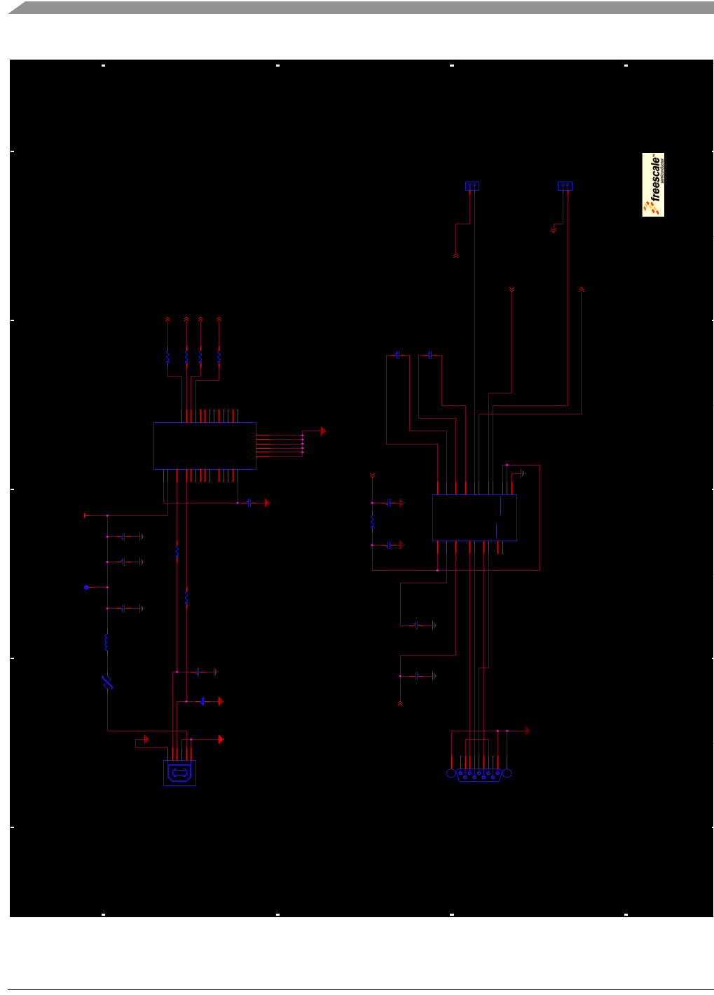
Figure 5-5. Schematic (5 of 5)
5
5
4
4
3
3
2
2
1
1
D D
C C
B B
A A
LCD_Vo_supply
DB4
DB5
DB6
VSS
Vo
VDD
RS
R/W
E
DB7
DB0
DB2
DB3
DB1
A_BKL+
V_LCD
PTD5
PTD7
PTF4
PTF5
PTF6
PTF7
PTD6
LCD_Vo_ref
Drawing Title:
Size Document Number Rev
Date: Sheet of
Page Title:
SCH-23731 PDF: SPF-23731 B1
1320X-QE128-EVB
C
Tuesday, February 05, 2008
LCD
77
Drawing Title:
Size Document Number Rev
Date: Sheet of
Page Title:
SCH-23731 PDF: SPF-23731 B1
1320X-QE128-EVB
C
Tuesday, February 05, 2008
LCD
77
Drawing Title:
Size Document Number Rev
Date: Sheet of
Page Title:
SCH-23731 PDF: SPF-23731 B1
1320X-QE128-EVB
C
Tuesday, February 05, 2008
LCD
77
Contrast
Adjust
CFAH1602B LCD Socket
Place R30 to enable the
negative voltage switcher
for the contrast adjust
Do not populate R38 and R31
NOTE:
PC1602 LCD Socket
R36
10K
R36
10K
R27
100K
R27
100K
R34
10K
R34
10K
R30 0 OHMR30 0 OHM
R28
5K
R28
5K
1 3
2
R33
10K
R33
10K
C30
0.1UF
C30
0.1UF
R37
10K
R37
10K
R35
10K
R35
10K
R29
383K
R29
383K
R26
4.7K
R26
4.7K
C33
1.0UF
C33
1.0UF
C34
1.0UF
C34
1.0UF
C32
10UF
C32
10UF
C31
1.0UF
C31
1.0UF
R31
0 OHM
DNP
R31
0 OHM
DNP
J16
1x16 TH SOCKET
J16
1x16 TH SOCKET
1
1
2
2
3
3
4
4
5
5
6
6
7
7
8
8
9
9
10
10
11
11
12
12
13
13
14
14
15
15
16
16
U6
LM2687
U6
LM2687
Cap+
1
GND
2
Cap-
3
SD
4VNEG 5
VFB 6
VOUT 7
VIN 8
J17
1x16 TH SOCKET
J17
1x16 TH SOCKET
1
1
2
2
3
3
4
4
5
5
6
6
7
7
8
8
9
9
10
10
11
11
12
12
13
13
14
14
15
15
16
16
R38 0 OHM
DNP
R38 0 OHM
DNP
Schematic and Bill of Material
1320x-QE128EVB Reference Manual, Rev. 0.0
5-6 Freescale Semiconductor
5.2 Bill of Materials
Table 5-1. Bill of Materials
Qty Part Reference Description Value Tolerance Manufacturer Manufacturer Part
Number
1 BT1 PCB Battery Holder
2xAA 2462 Keystone 2462
14 C1 C2 C3 C4
C12 C18 C19
C21 C22 C25
C26 C27 C28
C30
Ceramic Capacitor
X7R 0.1 µF 10% Venkel C0402X7R160-104KNE
1 C6 Ceramic Capacitor
COG 10pF 0.25pF Samsung CL05C100CO5NNNC
1 C7 Ceramic Capacitor
COG 1pF +/- 0.25pF Yageo America CC0402CRNPO9BN1R0
1 C8 Ceramic Capacitor
COG 10pF 5% Venkel C0402C0G500-100JNP
2 C9, C10 Ceramic Capacitor
COG 8pF 0.25pF Murata GRM1555C1H8R0CB01D
4 C11 C31 C33
C34 Ceramic Capacitor
X5R 1uF 10% AVX 0805YD105KAT2A
4 C13 C14 C17
C32 Ceramic Capacitor
X5R 10uF 10% Venkel C0805X5R100-106KNE
2 C15 C16 Ceramic Capacitor
COG 22pF 5% Venkel C0402C0G250-220JNE
1 C20 Ceramic Capacitor
X7R 10nF 10% Venkel C0402X7R500103KNE
3 C23 C24 C36 Ceramic Capacitor
X5R 4,7uF 10% Panasonic ECJ2FB1C475K
2 C37 C38 Ceramic Capacitor
COG 15pF 5% Venkel C0402C0G250-150JNP
4 D1 D2 D3 D4 SMD Power
Schottky Rectifier MBR0520LT1 On
Semiconductor MBR0520LT1G
2 F1 F2 Polyswitch
Overcurrent
Protection Device
500mA Raychem MICROSMD050F-2
2 VCC GND Test Point Pad TP-107-02-T Components
Corporation TP-107-02-T
4 J1 J6 J13 J15 Single Row Straight
pin Header TH 1X2 TSW-102-07-S-S Samtec TSW-102-07-S-S
1 J2 DC Power Jack
PCB, 2mm PJ-102AH CUI Stack PJ-102AH

Schematic and Bill of Material
1320x-QE128EVB Reference Manual, Rev. 0.0
Freescale Semiconductor 5-7
1 J3 Double Row Straight
pin Header TH 2X10 TSW-110-07-S-D Samtec TSW-110-07-S-D
1 J4 Double Row Straight
pin Header TH 2X16 TSW-116-07-S-D Samtec TSW-116-07-S-D
1 J5 Single Row Straight
pin Header TH 1X3 HTSW-103-07-S
M-S Samtec HTSW-103-07-SM-S
4 J7 J8 J10 J11 Double Row Straight
pin Header TH 2X8 TSW-108-07-G-
DSamtec TSW-108-07-G-D
1 J9 Double Row Straight
pin Header TH 2X3 TSW-103-07-S-
DSamtec TSW-103-07-S-D
1 J12 USB-series “B”
receptacle USB-B SINGATRON 2UB1505-000101
1 J14 Connector DB 9 TH DB 9 Tyco
Electronics 5747844-6
2 J16 J17 Socket TH 1X6 SSW-116-01-G-
SSamtec SSW-116-01-G-S
4 LED1 LED2
LED3 LED4 SMD Red top led HSMH-C190 Avago
Technologies HSMH-C190
1 LED5 SMD Green top led 597-5312-407F Dialight 597-5312-407F
1 LS1 SMD Speaker CMI-1240 CUI STACK CMI-1240
1 L1 L3 HF Chip coil 1,8nH 0,3nH TOKO,Inc LL1005-FHL1N8S
2 L2 L4 HF Chip coil 3,9nH 0,3nH TOKO,Inc LL1005-FHL3N9S
1 L5 Chip Ferrite Bead 500mA Steward LI0603E470R-10
1 Q1 P-channel MOSFET ZXM61P02F Zetex ZXM61P02F
1 Q2 NPN BJT MMBT3904LT1G On
Semiconductor MMBT3904LT1G
8 R1 R7 R11 R33
R34 R35 R36
R37
Fixed resistor RC31 10K 5% SEI Electronics
INC RMCF1/16S10K5%R
8 R2 R3 R5 R6 R8
R23 R24 R30 Fixed resistor RC31 0R 5% ROHM MCR01MZPJ000
5 R4 R12 R13
R15 R17 Fixed resistor RC31 390R 5% SMEC RC73L2Z391JTF
2 R9 R14 Fixed resistor RC31 100K 5% Panasonic ERJ2GEJ104X
1 R10 Fixed resistor RC31 1,5K 5% Yageo America RC0402JR-071K5L
3 R16 R18 R26 Fixed resistor RC31 4,7K 5% SMEC RC73L2Z472JTF
1 R19 Fixed resistor RC31 51K 5% Venkel CR0402-16W-513JT
4 R20 R21 R31
R38 Fixed resistor RC31 0R 5% ROHM MCR01MZPJ000
Table 5-1. Bill of Materials (continued)
Schematic and Bill of Material
1320x-QE128EVB Reference Manual, Rev. 0.0
5-8 Freescale Semiconductor
1 R25 Fixed resistor RC31 10R 5% Venkel
Company CR0402-16W-100JT
1 R27 Fixed resistor
RC32H 100K 1% Koa Speer RK73H1ETTP1003F
1 R28 SMT Potentiometer
Resistor 5K 20% Bourns 3314J-1-502E
1 R29 Fixed resistor
RC32H 383K 1% Koa Speer RK73H1ETTP3833F
4 R42 R43 R44
R45 Fixed resistor RC31 1K 5% Vishay
Intertechnology CRCW04021K00JNED
1 R46 Fixed resistor RC31 470K 5% Venkel CR0402-16W-474JT
1 SW1 Switch 4PDT TH 1-1437575-0 Tyco
Electronics 1-1437575-0
4 SW2 SW3 SW4
SW5 SMD Switch SPST EVQPHP03T Panasonic EVQPHP03T
1 U1 ZigBee Wireless
Transceiver MC13202 Freescale MC13202FC
1 U2 Low Dropout Voltage
Regulator LT1129CST-3.3#
PBF Linear
Technology LT1129CST-3.3#PBF
1 U3 EEPROM 128Kx8 AT24C1024BW Atmel AT24C1024BW
1 U5 RS-232 UART
Transceiver MAX3318EAP Maxim MAX3318EAP
1 U6 Low Dropout Voltage
Regulator LM2687 National
Semiconductor LM2687MMX
1 U7 USB UART, PB-free FT232R FTDI FT232RQ
1 Y1 Crystal SMD 16,00MHz +-10ppm NDK NX3225SA-16.000000MH
Z
1 Y2 Crystal SMD 32,768kHz +-20ppm Abracon ABS25-32.768-12.5-2-T
1 Z1 Transformer BALUN
SMD 2400MHz
50OHM Murata LDB212G4005C-001
1 P&E
MC9S08QE128
Daughter Board
MC9S08QE128_
Daughter_card P&E MC9S08QE128_
Daughter_card
1 STN LCD Daughter
Board 16x2 CFAH1602B Crystalfontz CFAH1602NYG-JP
Table 5-1. Bill of Materials (continued)