Freescale Semiconductor 1322X-NCB 1322x Network Node User Manual
Freescale Semiconductor, Inc. 1322x Network Node
Users Manual Revised

Document Number: 1322xNNRM
Rev. 1.1
07/2008
1322x Network Node
Reference Manual

How to Reach Us:
Home Page:
www.freescale.com
E-mail:
support@freescale.com
USA/Europe or Locations Not Listed:
Freescale Semiconductor
Technical Information Center, CH370
1300 N. Alma School Road
Chandler, Arizona 85224
+1-800-521-6274 or +1-480-768-2130
support@freescale.com
Europe, Middle East, and Africa:
Freescale Halbleiter Deutschland GmbH
Technical Information Center
Schatzbogen 7
81829 Muenchen, Germany
+44 1296 380 456 (English)
+46 8 52200080 (English)
+49 89 92103 559 (German)
+33 1 69 35 48 48 (French)
support@freescale.com
Japan:
Freescale Semiconductor Japan Ltd.
Headquarters
ARCO Tower 15F
1-8-1, Shimo-Meguro, Meguro-ku,
Tokyo 153-0064, Japan
0120 191014 or +81 3 5437 9125
support.japan@freescale.com
Asia/Pacific:
Freescale Semiconductor Hong Kong Ltd.
Technical Information Center
2 Dai King Street
Tai Po Industrial Estate
Tai Po, N.T., Hong Kong
+800 2666 8080
support.asia@freescale.com
For Literature Requests Only:
Freescale Semiconductor Literature Distribution Center
P.O. Box 5405
Denver, Colorado 80217
1-800-521-6274 or 303-675-2140
Fax: 303-675-2150
LDCForFreescaleSemiconductor@hibbertgroup.com
Information in this document is provided solely to enable system and software implementers to use
Freescale Semiconductor products. There are no express or implied copyright licenses granted
hereunder to design or fabricate any integrated circuits or integrated circuits based on the information
in this document.
Freescale Semiconductor reserves the right to make changes without further notice to any products
herein. Freescale Semiconductor makes no warranty, representation or guarantee regarding the
suitability of its products for any particular purpose, nor does Freescale Semiconductor assume any
liability arising out of the application or use of any product or circuit, and specifically disclaims any
and all liability, including without limitation consequential or incidental damages. “Typical” parameters
that may be provided in Freescale Semiconductor data sheets and/or specifications can and do vary
in different applications and actual performance may vary over time. All operating parameters,
including “Typicals”, must be validated for each customer application by customer’s technical
experts. Freescale Semiconductor does not convey any license under its patent rights nor the rights
of others. Freescale Semiconductor products are not designed, intended, or authorized for use as
components in systems intended for surgical implant into the body, or other applications intended to
support or sustain life, or for any other application in which the failure of the Freescale Semiconductor
product could create a situation where personal injury or death may occur. Should Buyer purchase
or use Freescale Semiconductor products for any such unintended or unauthorized application,
Buyer shall indemnify and hold Freescale Semiconductor and its officers, employees, subsidiaries,
affiliates, and distributors harmless against all claims, costs, damages, and expenses, and
reasonable attorney fees arising out of, directly or indirectly, any claim of personal injury or death
associated with such unintended or unauthorized use, even if such claim alleges that Freescale
Semiconductor was negligent regarding the design or manufacture of the part.
ARM is the registered trademark of ARM Limited. ARM7TDMI-S is the trademark of ARM Limited.
Freescale™ and the Freescale logo are trademarks of Freescale Semiconductor, Inc. All other
product or service names are the property of their respective owners.
© Freescale Semiconductor, Inc. 2005, 2006, 2007, 2008. All rights reserved.

1322x Network Node Reference Manual, Rev. 1.1
Freescale Semiconductor i
Contents
About This Book
Audience . . . . . . . . . . . . . . . . . . . . . . . . . . . . . . . . . . . . . . . . . . . . . . . . . . . . . . . . . . . . . . . . . . . . iii
Organization . . . . . . . . . . . . . . . . . . . . . . . . . . . . . . . . . . . . . . . . . . . . . . . . . . . . . . . . . . . . . . . . . iii
Revision History . . . . . . . . . . . . . . . . . . . . . . . . . . . . . . . . . . . . . . . . . . . . . . . . . . . . . . . . . . . . . . iii
Chapter 1
Safety Information
1.1 FCC Guidelines. . . . . . . . . . . . . . . . . . . . . . . . . . . . . . . . . . . . . . . . . . . . . . . . . . . . . . . . . . . . . . 1-1
1.2 FCC Labeling . . . . . . . . . . . . . . . . . . . . . . . . . . . . . . . . . . . . . . . . . . . . . . . . . . . . . . . . . . . . . . . 1-1
1.2.1 47 C.F.R. Sec. 15.21. . . . . . . . . . . . . . . . . . . . . . . . . . . . . . . . . . . . . . . . . . . . . . . . . . . . . . . 1-1
1.2.2 47 C.F.R. Sec.15.105(b) . . . . . . . . . . . . . . . . . . . . . . . . . . . . . . . . . . . . . . . . . . . . . . . . . . . . 1-2
1.2.3 47 C.F.R. Sec.15.203 . . . . . . . . . . . . . . . . . . . . . . . . . . . . . . . . . . . . . . . . . . . . . . . . . . . . . . 1-2
1.3 Regulatory Approval For Canada. . . . . . . . . . . . . . . . . . . . . . . . . . . . . . . . . . . . . . . . . . . . . . . . 1-2
1.4 Disposal Instructions. . . . . . . . . . . . . . . . . . . . . . . . . . . . . . . . . . . . . . . . . . . . . . . . . . . . . . . . . . 1-2
Chapter 2
1322x Network Node Module Overview and Description
2.1 Introduction. . . . . . . . . . . . . . . . . . . . . . . . . . . . . . . . . . . . . . . . . . . . . . . . . . . . . . . . . . . . . . . . . 2-1
2.2 Features. . . . . . . . . . . . . . . . . . . . . . . . . . . . . . . . . . . . . . . . . . . . . . . . . . . . . . . . . . . . . . . . . . . . 2-2
2.3 Board Level Specifications. . . . . . . . . . . . . . . . . . . . . . . . . . . . . . . . . . . . . . . . . . . . . . . . . . . . . 2-3
Chapter 3
System Overview and Functional Block Descriptions
3.1 System Block Diagram . . . . . . . . . . . . . . . . . . . . . . . . . . . . . . . . . . . . . . . . . . . . . . . . . . . . . . . . 3-1
3.2 System Overview . . . . . . . . . . . . . . . . . . . . . . . . . . . . . . . . . . . . . . . . . . . . . . . . . . . . . . . . . . . . 3-2
3.3 Power Management and Measurement. . . . . . . . . . . . . . . . . . . . . . . . . . . . . . . . . . . . . . . . . . . . 3-3
3.4 Low-cost 2.4 GHz ISM Band radio . . . . . . . . . . . . . . . . . . . . . . . . . . . . . . . . . . . . . . . . . . . . . . 3-4
3.5 USB Interface . . . . . . . . . . . . . . . . . . . . . . . . . . . . . . . . . . . . . . . . . . . . . . . . . . . . . . . . . . . . . . . 3-4
3.6 User Interface . . . . . . . . . . . . . . . . . . . . . . . . . . . . . . . . . . . . . . . . . . . . . . . . . . . . . . . . . . . . . . . 3-4
3.7 128x64 Pixel Monochrome Graphic LCD Display . . . . . . . . . . . . . . . . . . . . . . . . . . . . . . . . . . 3-5
3.8 Debug/Development Interfaces . . . . . . . . . . . . . . . . . . . . . . . . . . . . . . . . . . . . . . . . . . . . . . . . . 3-5
3.9 Audio Subsystem . . . . . . . . . . . . . . . . . . . . . . . . . . . . . . . . . . . . . . . . . . . . . . . . . . . . . . . . . . . . 3-5
3.10 GPIO Connector . . . . . . . . . . . . . . . . . . . . . . . . . . . . . . . . . . . . . . . . . . . . . . . . . . . . . . . . . . . . . 3-6
3.11 Clocks . . . . . . . . . . . . . . . . . . . . . . . . . . . . . . . . . . . . . . . . . . . . . . . . . . . . . . . . . . . . . . . . . . . . . 3-6
Chapter 4
Interface Locations and Pinouts
4.1 Overview. . . . . . . . . . . . . . . . . . . . . . . . . . . . . . . . . . . . . . . . . . . . . . . . . . . . . . . . . . . . . . . . . . . 4-1
4.2 Power Management . . . . . . . . . . . . . . . . . . . . . . . . . . . . . . . . . . . . . . . . . . . . . . . . . . . . . . . . . . 4-2
4.2.1 Supply Sources . . . . . . . . . . . . . . . . . . . . . . . . . . . . . . . . . . . . . . . . . . . . . . . . . . . . . . . . . . . 4-2
4.2.2 On/Off Switch and Power On Indicator . . . . . . . . . . . . . . . . . . . . . . . . . . . . . . . . . . . . . . . . 4-2

1322x Network Node Reference Manual, Rev. 1.1
ii Freescale Semiconductor
4.2.3 Power Measurement . . . . . . . . . . . . . . . . . . . . . . . . . . . . . . . . . . . . . . . . . . . . . . . . . . . . . . . 4-2
4.3 RF Circuitry . . . . . . . . . . . . . . . . . . . . . . . . . . . . . . . . . . . . . . . . . . . . . . . . . . . . . . . . . . . . . . . . 4-3
4.4 USB Connector (“B” Receptacle). . . . . . . . . . . . . . . . . . . . . . . . . . . . . . . . . . . . . . . . . . . . . . . . 4-3
4.5 LEDs, Switch, Buttons and Joystick. . . . . . . . . . . . . . . . . . . . . . . . . . . . . . . . . . . . . . . . . . . . . . 4-4
4.6 LCD Connector. . . . . . . . . . . . . . . . . . . . . . . . . . . . . . . . . . . . . . . . . . . . . . . . . . . . . . . . . . . . . . 4-5
4.7 Debug/Development Connectors . . . . . . . . . . . . . . . . . . . . . . . . . . . . . . . . . . . . . . . . . . . . . . . . 4-5
4.7.1 ARM JTAG Interface Connector . . . . . . . . . . . . . . . . . . . . . . . . . . . . . . . . . . . . . . . . . . . . . 4-5
4.7.2 Nexus Mictor Interface Connector . . . . . . . . . . . . . . . . . . . . . . . . . . . . . . . . . . . . . . . . . . . . 4-6
4.8 Audio Subsystem Connections . . . . . . . . . . . . . . . . . . . . . . . . . . . . . . . . . . . . . . . . . . . . . . . . . . 4-7
4.9 GPIO Connector . . . . . . . . . . . . . . . . . . . . . . . . . . . . . . . . . . . . . . . . . . . . . . . . . . . . . . . . . . . . . 4-7
4.10 FLASH Memory Recovery Jumpers and Erase . . . . . . . . . . . . . . . . . . . . . . . . . . . . . . . . . . . . . 4-8
4.11 ADC Voltage References . . . . . . . . . . . . . . . . . . . . . . . . . . . . . . . . . . . . . . . . . . . . . . . . . . . . . . 4-9
4.12 Jumper Selection. . . . . . . . . . . . . . . . . . . . . . . . . . . . . . . . . . . . . . . . . . . . . . . . . . . . . . . . . . . . 4-10
Chapter 5
Schematic, Board Layout, and Bill of Material

MC1322x Network Node Reference Manual, Rev. 1.1
Freescale Semiconductor iii
About This Book
This manual describes Freescale’s 1322x Network Node evaluation board. The 1322x Network Node
contains a Freescale third-generation, low power, 2.4 GHz radio frequency transceiver, with 32-bit ARM7
core based MCU, hardware acceleration for both the IEEE Standard 802.15.4 MAC and AES security, and
a full set of MCU peripherals into an 99-pin LGA Platform-in-Package (PiP).
Audience
This manual is intended for system designers.
Organization
This document is organized into 5 chapters.
Chapter 1 Safety Information — Highlights some of the FCC requirements.
Chapter 2 1322x Network Node Module Overview and Description — This chapter
introduces 1322x Network Node (NN) which is an IEEE, 802.15.4 compliant
evaluation board based on the Freescale MC1322x device.
Chapter 3 System Overview and Functional Block Descriptions — This section provides an
overview of the Network Node and block diagrams.
Chapter 4 Interface Locations and Pinouts — This chapter provides a description of the
interface locations and pinout of the 1322x Network Node circuit board.
Chapter 5 Schematic and Bill of Materials — This chapter provides the schematic, board
layout, and Bill of Materials (BOM).
Revision History
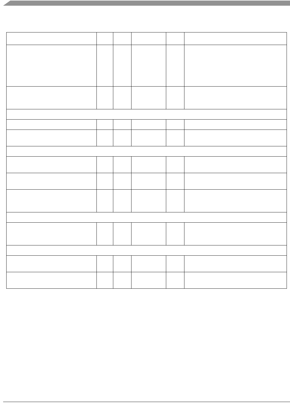
The following table summarizes revisions to this document since the previous release (Rev 1.0).
Revision History
Location Revision
Chapter 1 Updated FCC information.

MC1322x Network Node Reference Manual, Rev. 1.1
iv Freescale Semiconductor
Definitions, Acronyms, and Abbreviations
The following list defines the acronyms and abbreviations used in this document.
ADC Analog to Digital Converter
AES Advanced Encryption Standard
ARM Advanced RISC Machine
COG Chip on Glass
CTS Clear to Send
DAC Digital to Analog Converter
DMA Direct Memory Access
I2C Inter-Integrated Circuit is a multi-master serial computer bus
ISM Industrial Scientific Medical 2.4 GHz radio frequency band
JTAG Joint Test Action Group
LCD Liquid Crystal Display
LGA Land Grid Array
MAC Media Access Controller
MCU Microcontroller Unit
NEXUS An embedded processor development tool interface that helps design engineers
identify software and hardware-level issues.
NN Network Node
PCB Printed circuit board
PiP Platform in Package
PWM Pulse-width modulation
RTS Request to Send
SMA Connector Sub Miniature version “A” connector
SPI Serial Peripheral Interface
SSI Synchronous Serial Interface
TACT Switch A switch that provides a slight “snap” or “click” to the user to indicate function.
TELCO Telephone Company
USB Universal Serial Bus
VCP Virtual Com Port

1322x Network Node Reference Manual, Rev. 1.1
Freescale Semiconductor 1-1
Chapter 1
Safety Information
1.1 FCC Guidelines
This equipment is for use by developers for evaluation purposes only and must not be incorporated into
any other device or system. This device may not be sold to the general public. Integrators will be
responsible for reevaluating the end product (including the transmitter) and obtaining a separate FCC
authorization.
FCC approval of this device only covers the original configuration of this device as supplied. Any
modifications to this product, including changes shown in this manual, may violate the rules of the Federal
Communications Commission and make operation of the product unlawful.
1.2 FCC Labeling
FCC labels are physically located on the back of the board.
1.2.1 47 C.F.R. Sec. 15.21
This equipment has been tested and found to comply with the limits for a Class B digital device, pursuant
to part 15 of the FCC Rules. These limits are designed to provide reasonable protection against harmful
interference in a residential installation. This equipment generates, uses and can radiate radio frequency
energy and, if not installed and used in accordance with the instructions, may cause harmful interference
to radio communications. However, there is no guarantee that interference will not occur in a particular
installation. If this equipment does cause harmful interference to radio or television reception, which can
be determined by turning the equipment off and on, the user is encouraged to try to correct the interference
by one or more of the following measures:
• Reorient or relocate the receiving antenna.
• Increase the separation between the equipment and receiver.
• Connect the equipment into an outlet on a circuit different from that to which the receiver is
connected.
• Consult the dealer or an experienced radio/TV technician for help.

Safety Information
1322x Network Node Reference Manual, Rev. 1.1
1-2 Freescale Semiconductor
1.2.2 47 C.F.R. Sec.15.105(b)
This equipment complies with FCC radiation exposure limits set forth for an uncontrolled environment.
The antenna(s) used for this equipment must be installed to provide a separation distance of at least 8
inches (20cm) from all persons.
This device complies with Part 15 of the FCC Rules. Operation is subject to the following three
conditions:
1. This device may not cause harmful interference.
2. This device must accept any interference received, including interference that may cause undesired
operation.
3. This device is susceptible to electrostatic discharge (ESD) and surge phenomenon.
1.2.3 47 C.F.R. Sec.15.203
An intentional radiator shall be designed to ensure that no antenna other than that furnished by the
responsible party shall be used with the device. The use of a permanently attached antenna or of an
antenna that uses a unique coupling to the intentional radiator shall be considered sufficient to comply with
the provisions of this Section. The manufacturer may design the unit so that a broken antenna can be
replaced by the user, but the use of a standard antenna jack or electrical connector is prohibited. This
requirement does not apply to carrier current devices or to devices operated under the provisions of
Sections 15.211, 15.213, 15.217, 15.219, or 15.221. Further, this requirement does not apply to intentional
radiators that must be professionally installed, such as perimeter protection systems and some field
disturbance sensors, or to other intentional radiators which, in accordance with Section 15.31(d), must be
measured at the installation site. However, the installer shall be responsible for ensuring that the proper
antenna is employed so that the limits in this Part are not exceeded.
1.3 Regulatory Approval For Canada
This Class B digital apparatus complies with Canadian ICES-003 and RSS 210, Issue 7.
Cet appareil numérique de la classe B est conforme à la norme NMB-003 du Canada.
1.4 Disposal Instructions
This product may be subject to special disposal requirements. For product disposal instructions, refer to
www.freescale.com/productdisposal.
1322x Network Node Reference Manual, Rev. 1.1
Freescale Semiconductor 2-1
Chapter 2
1322x Network Node Module Overview and Description
2.1 Introduction
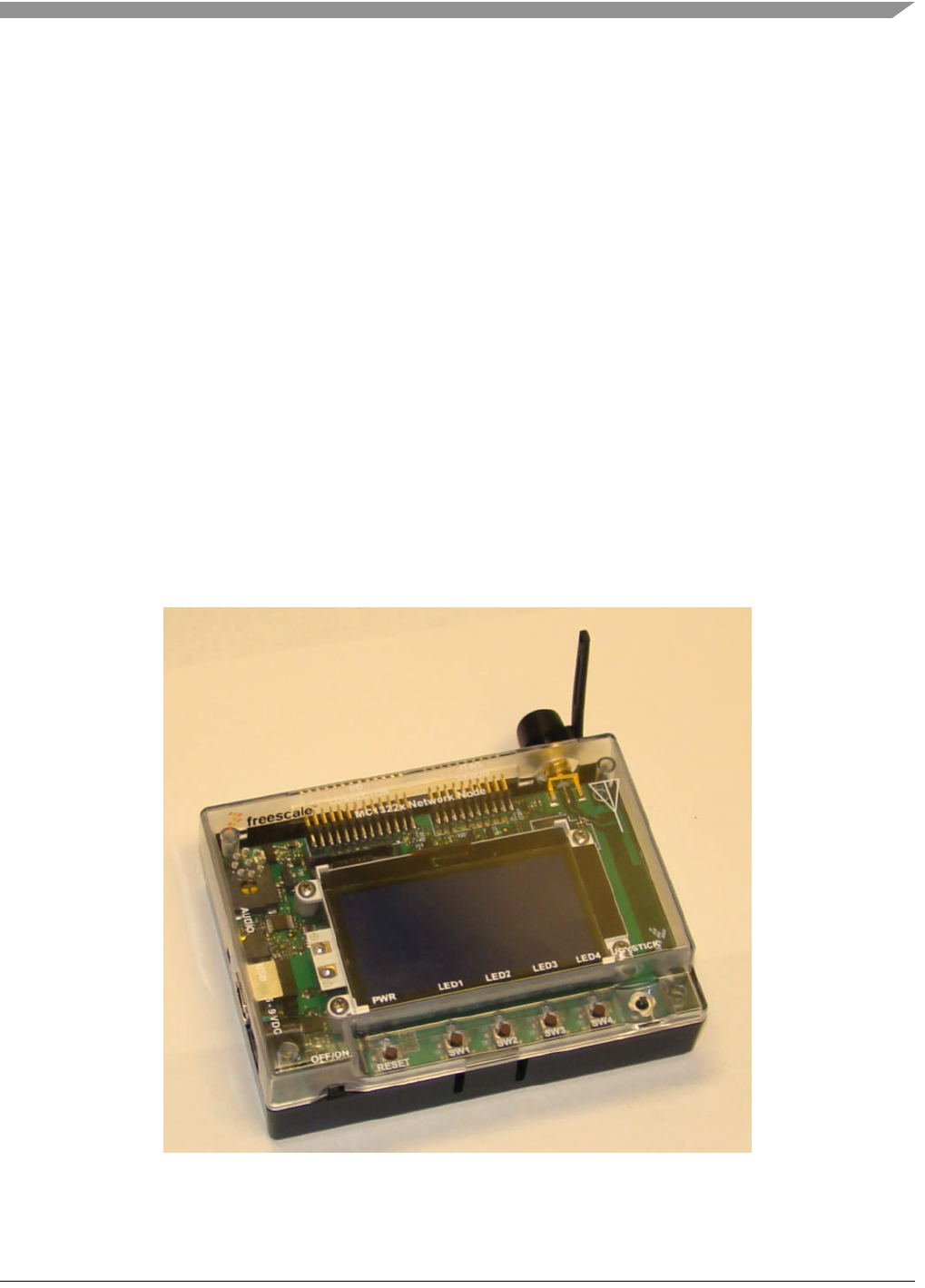
The 1322x Network Node (NN) is an IEEE 802.15.4 compliant evaluation board based on the Freescale
MC1322x device. The heart of the 1322x Network Node is Freescale’s MC1322x 99-pin LGA
Platform-in-Package (PiP) solution that can be used for wireless applications ranging from simple
proprietary point-to-point connectivity to complete ZigBee mesh networking. The MC1322x is designed
to provide a highly integrated, total solution, with premier processing capabilities and very low power
consumption.
The 1322x Network Node provides a platform to evaluate the MC1322x device, develop software and
applications, and demonstrate IEEE 802.15.4 and ZigBee networking capabilities. The Network Node
surrounds the core device with capabilities that provide a complete 802.15.4 radio, user interface,
debugging capabilities, connection to personal computers (PCs) and other devices, and portability.
Figure 2-1. 1322x Network Node

1322x Network Node Module Overview and Description
1322x Network Node Reference Manual, Rev. 1.1
2-2 Freescale Semiconductor
2.2 Features
The 1322x Network Node provides the following features:
• Full IEEE 802.15.4 compliant wireless node; ZigBee capable with Freescale’s BeeStack software
stack
• Based on Freescale’s third-generation MC1322x ZigBee platform which incorporates a complete,
low power, 2.4 GHz radio frequency transceiver, 32-bit ARM7 core based MCU, hardware
acceleration for both the IEEE 802.15.4 MAC and AES security, and a full set of MCU peripherals
into a 99-pin LGA Platform-in-Package (PiP)
• MC1322x provides a highly integrated, low cost RF node
— On-board balun and antenna switch in package
— Typical -95 dBm sensitivity
— Typical 0 dBm output power, with max approximately +2 dBm
— SMA connector with external antenna
• USB interface is bus-powered and full-speed compatible to the USB 2.0 and 1.1 specifications
• 128x64 pixel chip-on-glass monochrome, graphic LCD with LED backlight
• Audio subsystem
— 2.5mm audio jack for microphone and mono earpiece
— Input amplifier and anti-aliasing filter for an electret microphone
— Output path to second order analog filter from either 10-bit serial DAC or PWM as output
signal sources
— I2C controlled 32-position linear nonvolatile volume control for audio circuit
— Audio output amplifier for both earpiece or on-board dynamic speaker (switched by headset
jack)
• Two debug / development interfaces
— 20-pin connector for standard JTAG debug interface
— 38-pin MICTOR connector for extended NEXUS real-time debug interface
• Power management circuit with on-board regulation for multiple power sources
— Can be powered from USB interface, DC power jack or two AA batteries
— On/Off power switch
— Power-on green LED
• User interface switches and LEDs
— 4-directional TACT switch with center push for application purposes
— 4 pushbuttons for application purposes
— 4 processor controlled red LEDs for application purposes
— Reset switch
• 26-pin user header for selected General Purpose Input Output signals and data interfaces
• System clock options
— Default 24 MHz crystal reference oscillator (13 to 26 MHz crystal optional)
1322x Network Node Module Overview and Description
1322x Network Node Reference Manual, Rev. 1.1
Freescale Semiconductor 2-3
— Reference oscillator can be driven from an external source
— Optional 32.768 kHz crystal oscillator for accurate real-time delays
2.3 Board Level Specifications
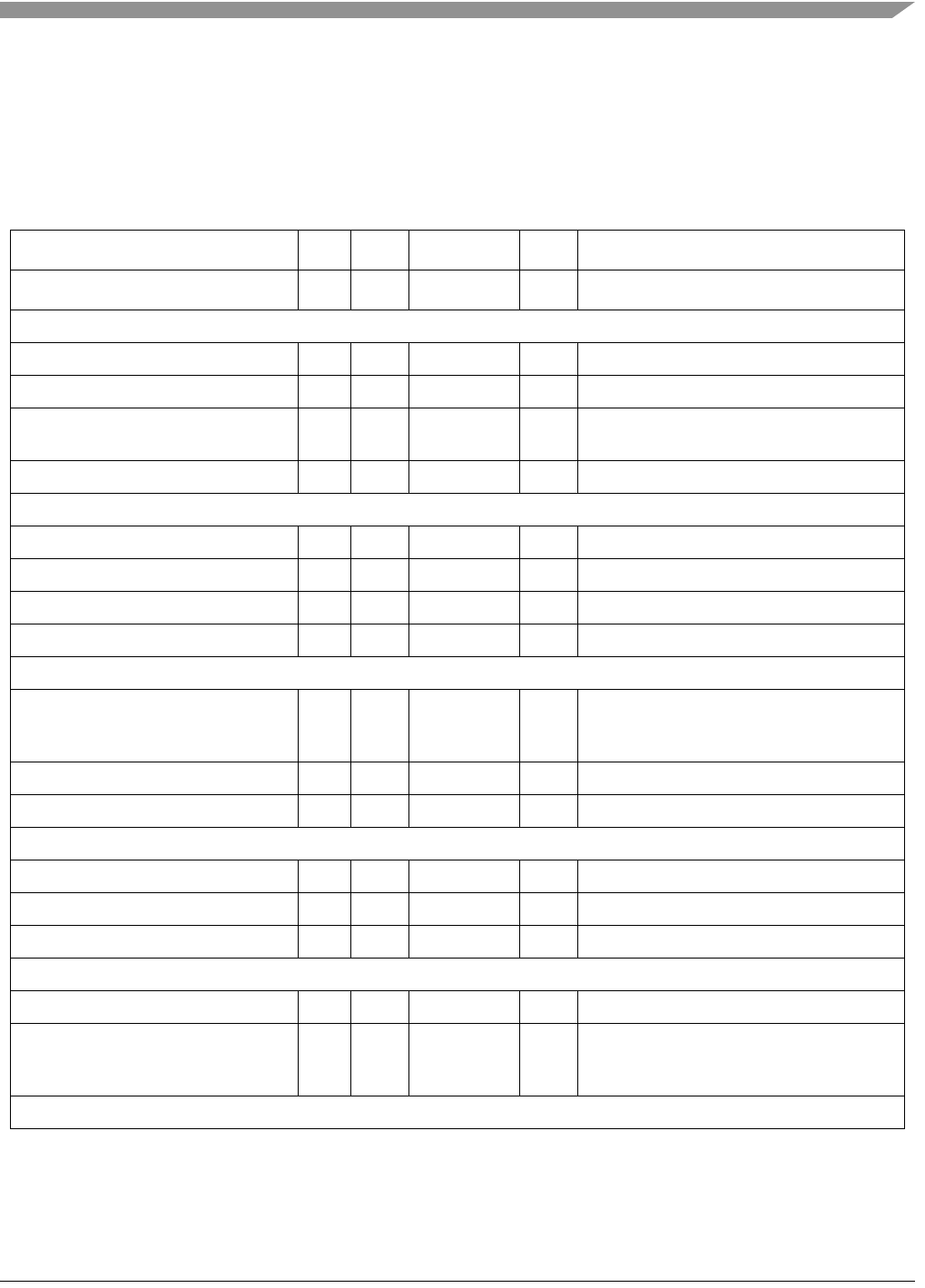
Table 2-1. 1322x Network Node Specifications
Parameter Units Notes/Conditions
MIN TYP MAX
General
Size (Enclosure: X, Y, Z) 135x100x40 mm
Size (PCB: X, Y) 125x85 mm
Layer build (PCB) 0.8 /
0.032
mm /
in
4-Layer
Dielectric material (PCB) FR4
Power
Voltage supply (DC) 4.4 5 12 V
Voltage supply (USB) 4.4 5 5.25 V USB 2.0/1.1 standard specification
Voltage supply (Batteries) 3 3.2 V
Current consumption 100 mA
Temperature
Operating temperature (see note) -20 +25 +85 °C The operating temperature is limited to
+70°C with the monochrome-graphic LCD
module mounted
Storage temperature -30 +25 +85 °C
USB interface USB 2.0 and 1.1 full-speed compatible
Audio
Audio (Input) -40 dB Accepts electret microphone element
Audio (Output)
Attenuation
RF
802.15.4 Frequency range 2405 2480 MHz All 16 channels in the 2450 MHz band
Range (outdoor / line of sight) 300 Meter <1% PER for 20-byte packets (point-to-point
in communications with 1322X Sensor
Reference Board)
RF Transmitter
1322x Network Node Module Overview and Description
1322x Network Node Reference Manual, Rev. 1.1
2-4 Freescale Semiconductor
802.15.4 Output power -30 0 +2 dBm Over range of Pout from IC control in 2 dB
steps.
Note: On channel 26, output power should
not exceed -5 dBm (power setting
0x0E) to meet FCC Part 15
requirements.
Harmonics
2nd harmonics
3rd harmonics
-30
-30dBm
dBm
Harmonics are compliant to ETSI and FCC
regulatory approval standards
RF Receiver
802.15.4 sensitivity -92 -95 dBm <1% PER for 20-byte packets
Proprietary high-speed sensitivity -80 dBm <1% PER for a minimum data payload of
400 packets
Regulatory Approval
FCC Product is approved accordingly to the FCC
part 15 standard
CE (ETSI) Product is approved accordingly to the EN
300 328 V1.7.1 (2006-10) standard
CE (EMC) Product is approved accordingly to the EN
301 489-1 V1.6.1 (2005-09) and EN 301
489-17 V1.2.1 (2002-08) standards
Safety
UL Product is approved accordingly to the IEC
60950-1 and EN 60950-1, First Edition
standards
Environment
RoHS Product complies with the EU Directive
2002/95/EC of 27 January 2003
WEEE Product complies with the EU Directive
2002/95/EC of 27 January 2003
Table 2-1. 1322x Network Node Specifications
Parameter Units Notes/Conditions
1322x Network Node Reference Manual, Rev. 1.1
Freescale Semiconductor 3-1
Chapter 3
System Overview and Functional Block Descriptions
This section provides an overview of the Network Node and block diagrams.
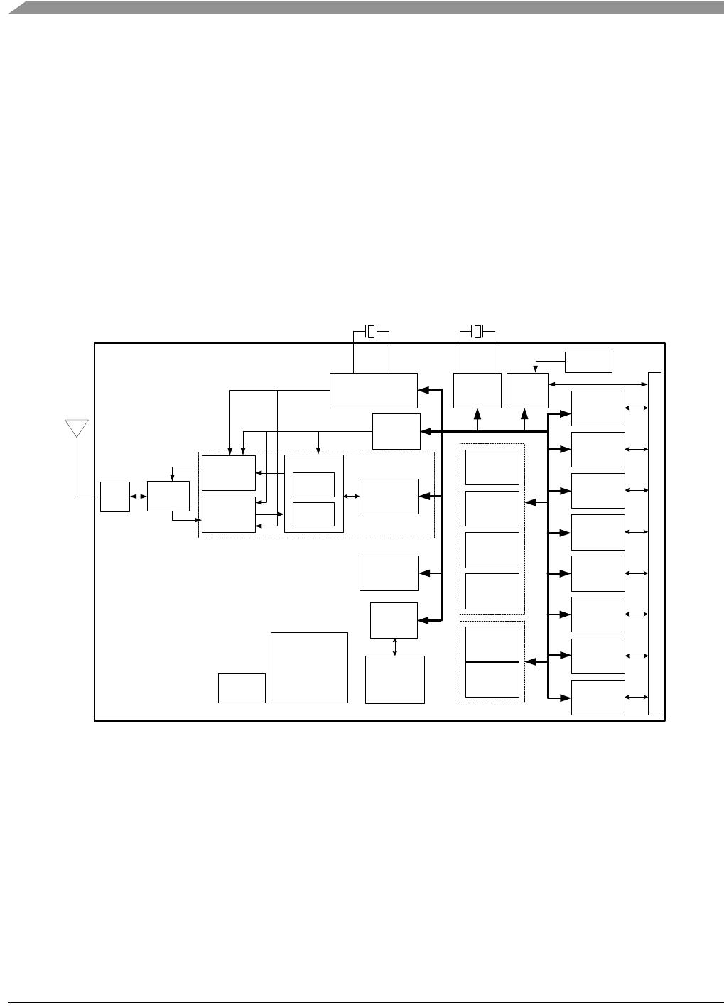
3.1 System Block Diagram
The following is the 1322x Network Node system level block diagram.
Figure 3-1. 1322x Network Node Block Diagram
24 MHz 32.768
KHz
Audio
Output
DAC
DAC101S101
Earphone
Power
Manage-
ment
DC Adaptor
2xAA Battery
USB Bus Power
VCC
MC13224V/225V
Advanced ZigBee™- Compliant PiP
Ext
Clock
Source
13-26MHz Clk Clk
Debug
Interface
38-Pin
MICTOR
Conn
NEXUS
NEXUS
Debug
Interface
20-Pin
JTAG
Conn
JTAG
JTAG
Power
Measure-
ments
128x64
Monochrome
Graphic LCD
Optrex
(OPTREX
#F-51553)
LCD
Step-Up
DC-DC
Converter
SMA Connector
Audio
Mic Input w/
Amp / LP
Filter
ADC Mic
SSI
TMR3 - PWM Audio
Output
Amp / LP
Filter
Audio
Volume
Control
MAX5434
Audio
Amp
NCP4896 Speaker
GPIO
26-Pin
Header
GPIO User
Apps
USB
Interface
FT232RQ
UART USB
Conn
GPIO 4 Push Buttons,
Joystick,
Reset Switch,
On/Off Switch
GPIO 4 Red LEDs,
1 Green LED
System Overview and Functional Block Descriptions
1322x Network Node Reference Manual, Rev. 1.1
3-2 Freescale Semiconductor
3.2 System Overview
The heart of the 1322x Network Node is Freescale’s MC1322x 99-pin LGA Platform-in-Package (PiP)
solution that can be used for wireless applications ranging from simple proprietary point-to-point
connectivity to complete ZigBee mesh networking. The MC1322x is designed to provide a highly
integrated, total solution, with premier processing capabilities and very low power consumption.
The MC1322x MCU resources offer superior processing power for ZigBee and IEEE 802.15.4
applications. A full 32-bit ARM7TDMI-S core operates up to 26 MHz. A 128 Kbyte FLASH memory is
mirrored into a 96 Kbyte RAM for upper stack and applications software. In addition, an 80 Kbyte ROM
is available for boot software, peripheral device drivers, standardized IEEE 802.15.4 MAC and
communications stack software. A full set of peripherals and Direct Memory Access (DMA) capability for
transceiver packet data complement the processor core.
Figure 3-2. MC1322x Block Diagram
On-board peripherals include
• Two dedicated UART modules capable of 2Mbps with CTS/RTS support
• SPI port with programmable master and slave operation
• Keyboard interface capability.
• Two 12-bit analog-to-digital converters (ADCs) with 8 input channels
• Four independent 16-bit timers with PWM capability.
• Inter-integrated circuit (I2C) interface
• Synchronous Serial Interface (SSI) with I2S and SPI capability and FIFO data buffering
TIMER
MODULE
(TMR)
(4 Tmr Blocks)
UART
MODULE
(UART0)
UART
MODULE
(UART1)
SYNC SERIAL
INTERFACE
(SSI/i2S)
KEYBOARD
INTERFACE
(KBI)
INTER-IC BUS
MODULE
(I2C)
SERIAL
PERIPHERAL
INTERFACE
(SPI)
DUAL
12-BIT
ADC
MODULE
GPIO and IO
CONTROL
UP TO 64 IO PINS
ARM7
TDMI-S
32-BIT
CPU
BUS
INTERFACE
& MEMORY
ARBITRATOR
ARM
INTERRUPT
CONTROLLER
(AITC)
JTAG/
Nexus
DEBUG
ADVANCED
SECURITY
MODULE
(ASM)
CLOCK &
RESET
MODULE
(CRM)
RADIO
INTERFACE
MODULE
(RIF)
96KBYTE
SRAM
(24K WORDS x
32 BITS)
80KBYTE
ROM
(20KWORDS x
32 BITS)
RF
OSCILLATOR
&
CLOCK GENERATION
SPI
FLASH
MODULE
(SPIF)
802.15.4
MAC
ACCELERATOR
(MACA)
DIGITAL
MODEM
TX
MODEM
RX
MODEM
128KBYTE
NON-VOLATILE
MEMORY
(SERIAL
FLASH)
ANALOG
TRANSMITTER
ANALOG
RECEIVER
RF
TX/RX
SWITCH
IEEE 802.15.4 TRANSCEIVER
BALUN
ANALOG
POWER
MANAGEMENT
&
VOLTAGE
REGULATION
MC13225
Platform-in-Package (PiP)
IEEE 802.15.4/ZIGBEE SOLUTION
Buck
Regulator
24 MHz (typ) 32.768 KHz (optional)
BATTERY
DETECT
System Overview and Functional Block Descriptions
1322x Network Node Reference Manual, Rev. 1.1
Freescale Semiconductor 3-3
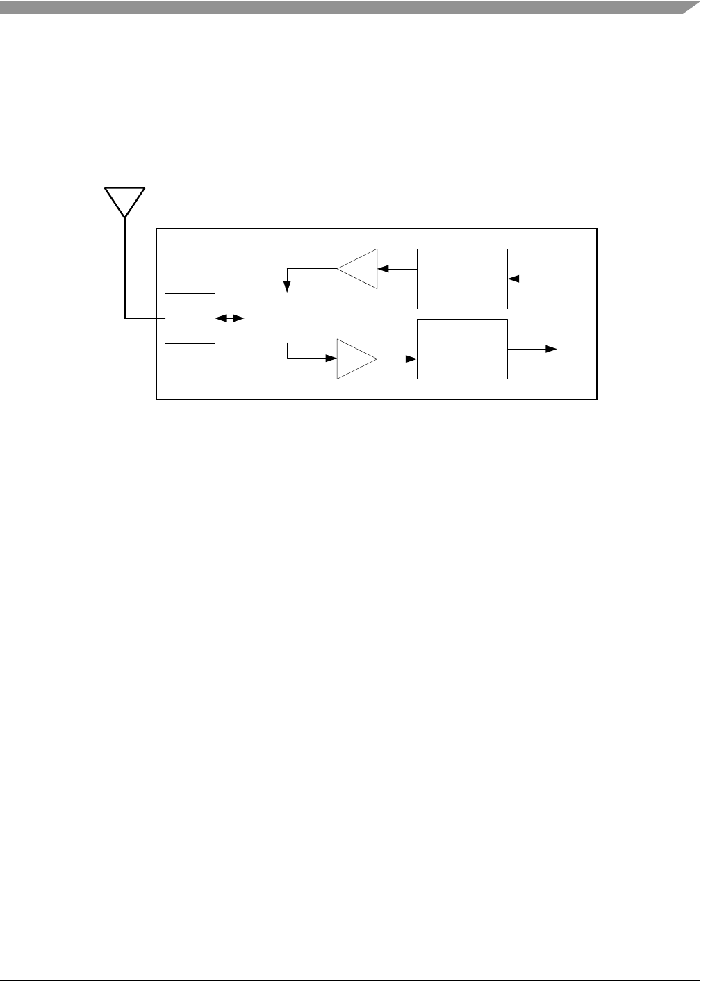
The RF radio interface provides for low cost and high density as shown in Figure 3-3. An onboard balun
along with a TX/RX switch allows direct connection to a single-ended 50-Ω antenna. The integrated PA
provides programmable output power typically from -30 dBm to +2dBm, and the RX LNA provides -95
dBm sensitivity. This solution also has onboard bypass capacitors and crystal load capacitors for the
smallest footprint in the industry. All components are integrated into the package except the crystal and
antenna.
Figure 3-3. MC1322x RF Interface
Augmenting the core device on the Network Node are:
• Low-cost 2.4 GHz ISM Band radio
• 2.0 USB connection
• User interface with pushbuttons, LEDs and 128x64 pixel graphic LCD
• Versatile power sources and management
• Debug / development ports
• Audio subsystem
• GPIO connector for system expansion
Users are encouraged to reference the board schematic for the following sections.
3.3 Power Management and Measurement
To allow maximum versatility, the Network Node can be powered via a DC source (typically an AC-DC
converter; nominally 5 Vdc), the USB node, or an onboard battery pack with 2 AA alkaline batteries.
• The DC source or USB will automatically shutdown the battery supply.
• The DC source and the USB power are regulated to 3.3 V, however, the raw battery pack voltage
directly supplies the circuitry
• All sources are isolated via diodes.
• An on/off switch and a power-on LED are provided (see Section 4.2.2, “On/Off Switch and Power
On Indicator”).
• Zero-ohm resistors are provided to allow isolation and measurement of various system components
(see Section 4.2.3, “Power Measurement”)
ANALOG
TRANSMITTER
ANALOG
RECEIVER
RF
TX/RX
SWITCH
BALUN
LNA
PA
System Overview and Functional Block Descriptions
1322x Network Node Reference Manual, Rev. 1.1
3-4 Freescale Semiconductor
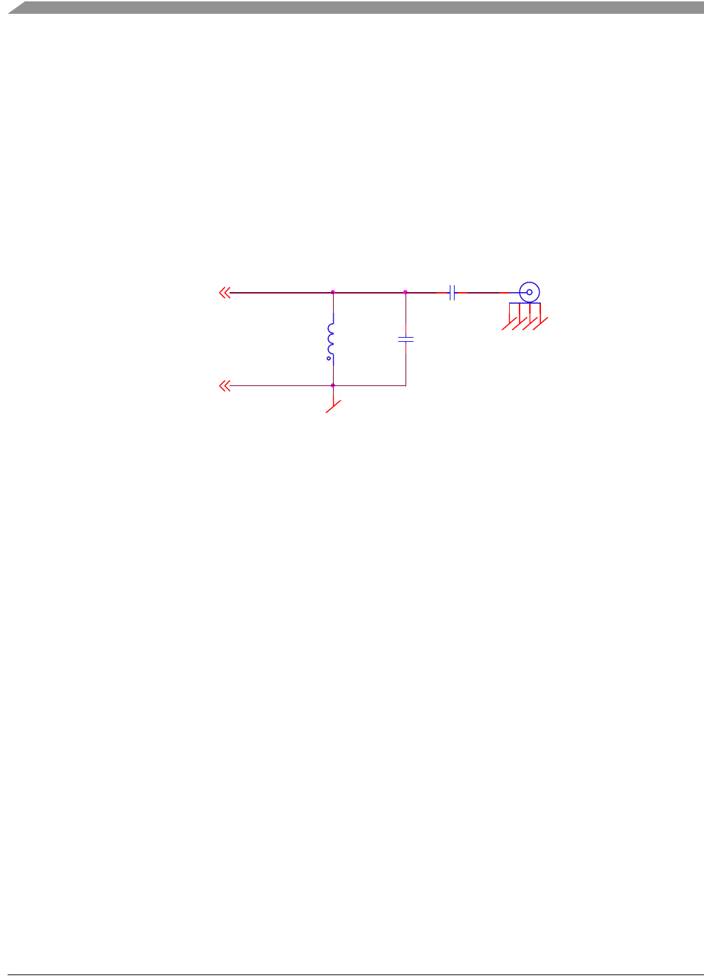
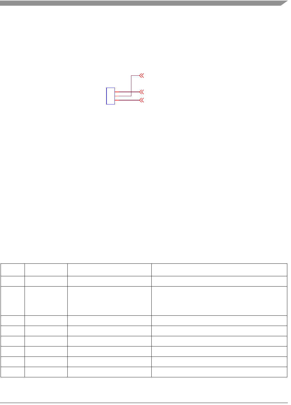
3.4 Low-cost 2.4 GHz ISM Band radio
The MC1322x provides an onboard balun, antenna switch, and LNA. The only external component
required for the radio is an antenna. The Network Node provides a PCB-mounted SMA that connects to
an external antenna for a complete solution. Figure 3-4 shows the RF network external to the MC1322x.
• Typical output power is 0 dBm, with +2 dBm max
• Typical sensitivity is -95 dBm.
• Frequency range is 2405 to 2480 MHz
• Typical range (outdoors, line of sight) is 300 meters
Figure 3-4. Network Node RF Network
Freescale recommends using the provided SMA connector to mount the provided antenna (see Section 4.3,
“RF Circuitry”).
3.5 USB Interface
For many applications or demonstrations it is desirable to connect the Network Node to a PC or other
device. A USB port is provided with a USB “B” receptacle plug. The port is connected to a FTDI FT232R
USB UART device that appears as a Virtual COM port (VCP) to the PC. PC drivers are available with the
module.
The USB interface is configured as a "Bus Powered" device and will therefore draw all required power
from the USB interface. The device is USB 2.0 full speed compatible.
3.6 User Interface
The Network Node provides multiple means for user interface for both debug and demonstration.
• Four individual pushbuttons can be used as input, and a 4-direction tactile joystick switch with
center push is wired in parallel with the individual pushbuttons. These pushbuttons have interrupt
generation capability.
• Four individual LEDs can be used as indicators for debug or status.
J7
SMA
L1
3.9nH
Not Mounted
C3
1pF
Not Mounted
RF_RX_TX
RF
C54
10pF
RF_GND

System Overview and Functional Block Descriptions
1322x Network Node Reference Manual, Rev. 1.1
Freescale Semiconductor 3-5
3.7 128x64 Pixel Monochrome Graphic LCD Display
The Network Node supports a 128x64 pixel chip-on-glass (COG) STN transmissive monochrome graphic
LCD that provides for alpha-numeric or graphic readout. The LCD module is mounted on top of the main
circuit board and connects via a flat flex cable (FFC).
• The display is an OPTREX #F-51553GNBJ-LW-AB
• Viewing area is 66.8 (W) × 35.5 (H) mm
• The LCD operates from 5 Vdc generated from the main operating voltage. The LCD module
requires a highly regulated 5 V so that the high voltages generated onboard the display are
consistent.
• The LCD has white LED backlighting with a typical current of 40 mA when full on. The
backlighting is switched by a FET and can be modulated to save current and vary the intensity.
• LCD interface to the MCU is via an 8-bit parallel interface
• The onboard controller is a member of the Epson S1D15605 Series family with an integrated
display data RAM
3.8 Debug/Development Interfaces
There are two separate debug ports (for pinouts see Section 4.7, “Debug/Development Connectors”). A
20-pin connector is provided for a standard JTAG debug interface. This a lower cost option that only
requires a simple interface cable to connect to the PC and use standard ARM software development tools.
A separate 38-pin Mictor connector is uniquely provided on this module to support the extended capability
Nexus real-time debug interface for the ARM processor.
3.9 Audio Subsystem
The audio subsystem provides means for simple output sounds/tones or for TELCO voice quality audio.
• A 2.5mm stereo jack is provided to interface to a typical telephone-type headset with an electret
microphone and a single earphone.
• Audio input - The audio input is taken from the headset electret microphone (mic).
— An onboard 10 k-ohm resistor circuit biases the mic for an ~1 Vdc operating voltage.
— The mic AC signal is filtered and amplified through a active low-pass filter with a voltage gain
of about 30 (~30 dB). The filter topology is a multiple feedback (MFB) 3-pole, linear phase
design. The target cutoff frequency is 3.6 kHz. The filter is intended as an anti-aliasing filter
for sampled data.
— The input amplifier output is sampled via the onboard MC1322x ADC. The sampling
frequency is programmable.
• Audio output source - The audio output can be sourced from both a serial 10-bit DAC and a PWM
timer output.
— The 10-bit serial DAC uses the SSI port to send provide the digital sample data.
— The PWM timer output is typically modulated to create a Class-D amplifier. Secondarily, a
simple 50% duty cycle signal can provide simple tones.

System Overview and Functional Block Descriptions
1322x Network Node Reference Manual, Rev. 1.1
3-6 Freescale Semiconductor
— The audio output source is jumper selectable via J10
• Audio output processing - The DAC or PWM out signal is filtered through an active 2-pole LPF.
From the filter the signal passes through a passive attenuator, and then is amplified and driven to
either an on-board speaker or the headset earphone.
— The attenuator provides a volume control that is controlled via a software 32 linear tap
programmable, non-volatile digital potentiometer. The interface to the potentiometer is the I2C
port.
— The onboard speaker is automatically disconnected if a headset is plugged-in.
3.10 GPIO Connector
The GPIO connector (J2) provides a number of data interfaces and GPIO for external system expansion,
Section 4.9, “GPIO Connector” gives details.
• A number of the GPIO are shared with the LCD interface. User should take care to avoid conflict
and may have to disable LCD to use some GPIO or ports.
• Power supply voltage is provided
— Current draw should be limited to 50 mA.
— A separate regulated voltage can be enabled.
• Provision is made to supply an external reference clock if desired.
3.11 Clocks
The 1322x Network Mode provides for two system clock sources.
• MC1322x Reference Oscillator - The default frequency for the reference oscillator is 24 MHz and
the mounted crystal X1 is a 24 MHz device that meets MC1322x specifications. There are two
additional options for the module
— X1 can be replaced by 13-26 MHz crystal (it must meet MC1322x specifications), however,
the onboard PLL must be used in this case. The PCB provides for PLL filter components, but
these are not populated.
— An external clock source can be supplied as the reference source (typically 24 MHz). The
frequency must accurate to +/-40ppm. The external clock source is supplied through GPIO
Connector J2, and crystal X1 must be removed and capacitor C58 mounted (see Chapter 5,
“Schematic, Board Layout, and Bill of Material”, Sheet 1).
— 32.768 kHz Crystal Oscillator - Provision is also made for an optional secondary 32.768 kHz
crystal X2. This oscillator can be used for a low power accurate timebase. The module comes
without this crystal and its load capacitors C7 and C12 unmounted (see Chapter 5, “Schematic,
Board Layout, and Bill of Material”, Sheet 1).
1322x Network Node Reference Manual, Rev. 1.1
Freescale Semiconductor 4-1
Chapter 4
Interface Locations and Pinouts
This chapter provides a description of the interface location and pinout of the 1322x Network Node PCB.
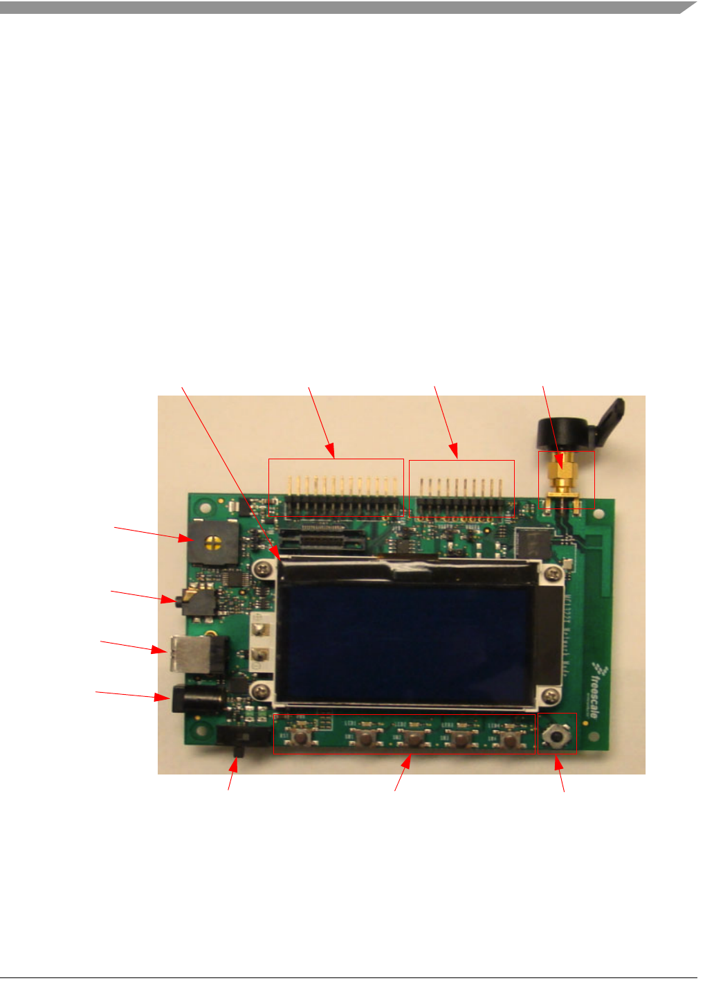
4.1 Overview
This chapter provides the locations (as shown in Figure 4-1) and descriptions of switches, jumpers, and
connectors on the 1322x Network Node PCB. Users should reference the figures in the subsequent sections
while moving through this chapter and reference the circuit board schematic in Chapter 5, “Schematic,
Board Layout, and Bill of Material”, for additional information.
Figure 4-1. Network Node PCB Top View
F
Tact SwitchesOn-Off Switch
JTAG ConnectorGPIO Connector
USB
DC
Supply
Joystick
RF ConnectorLCD Display
Audio
Connector
Buzzer
Interface Locations and Pinouts
1322x Network Node Reference Manual, Rev. 1.1
4-2 Freescale Semiconductor
4.2 Power Management
The module can be powered from the DC power jack, the USB port, or the battery pack.
4.2.1 Supply Sources
Table 4-1 lists the supply sources, connectors, and voltages. Board maximum current draw is rated at 100
mA.
Table 4-1. Power Supply Sources
4.2.2 On/Off Switch and Power On Indicator
The following are used with the power management:
• Switch SW7 - 4-pole slide switch disconnects ALL sources
• Green LED D5 - indicates power from any source
4.2.3 Power Measurement
It is possible to isolate various circuit blocks to measure current draw via 0-ohm resistors. The resistors
are all mounted as default.
Below is a list of the supplies.
• R68 -> VCC (Output from on-board regulator)
• R65 -> VBATT (Supply for 1322x)
• R80 -> V_DIS (Supply for display circuit)
• R43 -> V_AUD (Supply for audio circuit)
• R64 -> 3V (Output from on-board regulator for GPIO customer access), or alternately, R66 (not
mounted) can enable separate regulator U12.
Source Connector Min
(Volts) Typical
(Volts) Max
(Volts) Notes
DC Source J5 4.4 5 12 Use DC only source. The connector is a 2 mm DC power
jack; positive center conductor.
USB J6 4.4 5 5.25
AA Battery
Pack
BC1 ~2.0 3 3.2 Two AA cells. Battery pack is automatically disabled by
either DC source or USB. Accessible through the door on
the bottom of the plastic enclosure.
Interface Locations and Pinouts
1322x Network Node Reference Manual, Rev. 1.1
Freescale Semiconductor 4-3
4.3 RF Circuitry
The external antenna is connected via the provided SMA connector (J7).
NOTE
Only the provided Antenova® antenna (model Titanus) should be used with
this module. This RF design has been certified with this antenna.
Figure 4-2. Antenova® Titanus Model Antenna
4.4 USB Connector (“B” Receptacle)
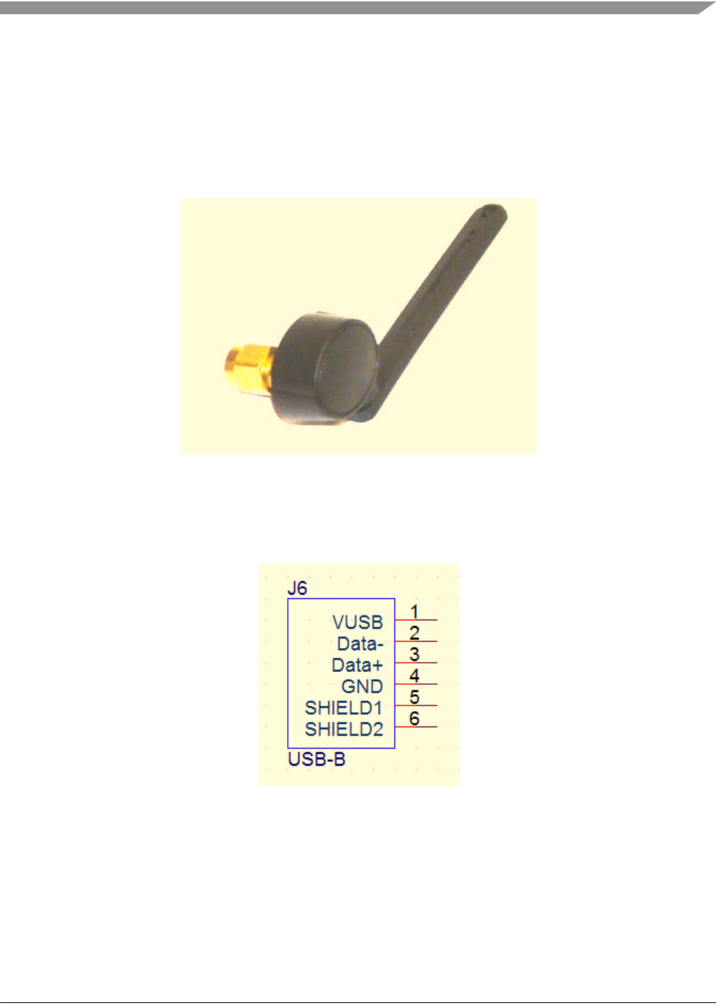
The USB connector is designated as J6. Figure 4-3 shows the connector pinout.
Figure 4-3. USB Connector Pinout

Interface Locations and Pinouts
1322x Network Node Reference Manual, Rev. 1.1
4-4 Freescale Semiconductor
4.5 LEDs, Switch, Buttons and Joystick
The Network Node contains a total four red LEDs and one green LED
• The four red LEDs are driven by the MCU and controlled by the software application.
• As previously stated, the green LED is directly connected to the on-board regulator and acts as a
"Power On" indication.
As also previously stated, SW7 is an on/off slide switch that connects the power supplies.
There are five pushbuttons total.
• One pushbutton (SW5) is separate and provides a master hardware Reset.
• Four additional pushbuttons are connected to the MCU GPIO for software application. These
buttons all have interrupt generation capability
A joystick (SW6) is also provided.
• The joystick is a 4-direction TACT Switch with Center Push.
• The 4-directional TACT switches are connected in parallel with the four user pushbuttons.
• The center push switch is separate and does not have interrupt generation capability
Table 4-2. Switch and LED Summary
Item GPIO Connection Feature
PWR (green) VCC ‘Power On’ indication
LED1 (red) KBI_1 Application specific
LED2 (red) KBI_2 Application specific
LED3 (red) KBI_3 Application specific
LED4 (red) TX_ON Application specific
SW1 (pushbutton) KBI_4 Interrupt functionality. In parallel with SW6 (right).
SW2 (pushbutton) KBI_5 Interrupt functionality. In parallel with SW6 (down).
SW3 (pushbutton) KBI_6 Interrupt functionality. In parallel with SW6 (left).
SW4 (pushbutton) KBI_7 Interrupt functionality. In parallel with SW6 (up).
SW5 (RST) RESETB HW reset
SW6 (right) KBI_4 Interrupt functionality. In parallel with SW1.
SW6 (down) KBI_5 Interrupt functionality. In parallel with SW2.
SW6 (left) KBI_6 Interrupt functionality. In parallel with SW3.
SW6 (up) KBI_7 Interrupt functionality. In parallel with SW4.
SW6 (center) KBI_0_HST_WK Host wake up output functionality. No interrupt functionality
Interface Locations and Pinouts
1322x Network Node Reference Manual, Rev. 1.1
Freescale Semiconductor 4-5
4.6 LCD Connector
The LCD module is connected to the main circuit board via a 30-conductor flat flex cable (FFC) with 0.5
mm spacing. The main board connector is an FFC, Right Angle Dip, zero insertion force (ZIF), 30 pin
connector (J13).
NOTE
The LCD connector is a ZIF unit. Be sure to release the connector before
trying to connect or disconnect the FFC to the LCD.
4.7 Debug/Development Connectors
4.7.1 ARM JTAG Interface Connector
The MC1322x supports connection to a subset of the defined ARM JTAG connector. The JTAG interface
is a standard 2.54mm/0.1inch spacing, 20-pin debug interface (J1). The 20-pin connector is clearly
separated from the GPIO pin header (J2) and located at the rear side of the module. The 20-pin connector
has Pin 1 marking for correct plug-in of the development cable.
Table shows the device pins that are connected to the associated JTAG header pin outs if the JTAG
connector is used.
Table 4-3. ARM JTAG 20-Pin Connector Assignments (J1)
Name1
1NC means No Connect.
Pin # Pin # Name
VCC 1 2 VCC
NC2
2MC1322x does not support separate JATG reset TRST.
34GND
TDI 5 6 GND
TMS 7 8 GND
TCK 9 10 GND
RTCK 11 12 GND
TDO 13 14 GND
RESET3
3VCC through a 100k-ohm pullup.
15 16 GND
NC 17 18 GND
NC 19 20 GND

Interface Locations and Pinouts
1322x Network Node Reference Manual, Rev. 1.1
4-6 Freescale Semiconductor
4.7.2 Nexus Mictor Interface Connector
The MC1322x also supports connection to a subset of the defined Nexus Mictor connector. The hardware
interface is a 38-pin Mictor 0.64mm/0.025inch spacing target connector (J11). Table 4-4 shows the device
pins that are connected to the associated Mictor pinouts. The 38-pin MICTOR connector has a "plug
security" for avoid reverse plug-in. J11 is located on the bottom side of the main board.
Table 4-4. Nexus 38-Pin Mictor Connector Assignments (J11)
Name1
1NC means No Connect.
Pin # Pin # Name
NC 1 2 NC
NC 3 4 NC
NC 5 6 RTCK
NC 7 8 NC
VCC (pullup)2
2VCC through a 100k-ohm pullup.
9 10 EVTI_B
TDO 11 12 VCC3
3VCC isolated by a 1k-ohm resistor.
NC 13 14 RDY_B
TCK 15 16 MDO07
TMS 17 18 MDO06
TDI 19 20 MDO05
RESET4
4VCC through a 100k-ohm pullup.
21 22 MDO04
NC 23 24 MDO03
NC 25 26 MDO02
NC 27 28 MDO01
NC 29 30 MDO00
NC 31 32 EVTO_B
NC 33 34 MCKO
NC 35 36 MSEO1_B
NC 37 38 MSEO0_B
Interface Locations and Pinouts
1322x Network Node Reference Manual, Rev. 1.1
Freescale Semiconductor 4-7
4.8 Audio Subsystem Connections
The audio subsystem uses the following connections:
• 2.5mm stereo jack J12 - for headset mic and earphone
• Jumper J10 - selects audio output source. See Figure 4-4 for connections.
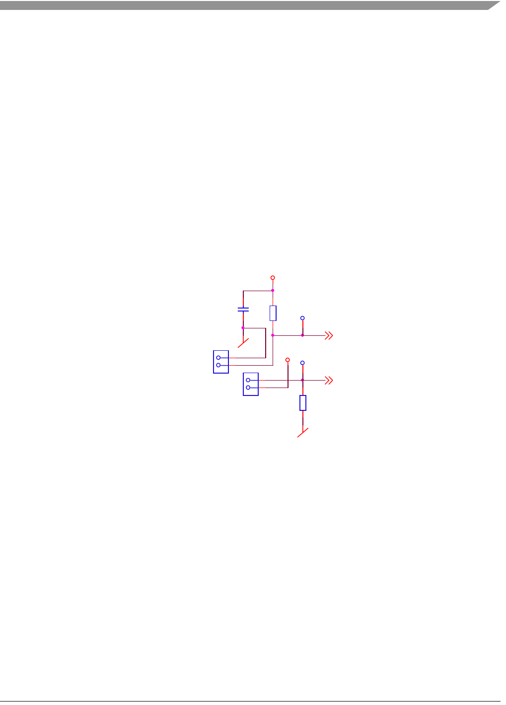
Figure 4-4. J10 Audio Output Source Jumper
4.9 GPIO Connector
The GPIO connector (J2) is a standard 2.54mm/0.1inch spacing, 26-pin header. The connector provides
access to MCU GPIO, an external clock source connection, a timer output, ADC inputs, the SSI port, a
UART port, the SPI port, the I2C port, and the serial DAC output. Power is also provided on the connector.
• VCC is the main supply voltage. Current draw should be limited to 50 mA.
• CLKIN can be used to supply an external reference clock (nominally 24 MHz). The onboard
crystal must be removed and an ac-coupling capacitor added.
• A number of the GPIO are shared with the LCD interface. Best practice is to disable the LCD data
interface to used these signals (see Table 4-5 below).
• The serial DAC output is available at the connector. The DAC output should not be selected as the
output audio source (J10) when used offboard.
Table 4-5. GPIO Connector J2 Pinouts
Pin Name Function Notes
1 TMR1 Timer I/O or GPIO Hardwired to LCD control output.
2 CLKIN Source for external clock to
reference oscillator
• 13-26 MHz reference clock with <40 ppm accuracy
• Onboard crystal must be removed
• Enable signal to MC1322x by adding C58, 10pF; see
schematic
3 VCC Voltage supply from module 3V output from on-board regulation
4 GND System ground
5 ADC1 ADC Analog Input Channel or GPIO
6 ADC2 ADC Analog Input Channel or GPIO Hardwired to LCD data buffer. Use Jumper J14 to disable.
7 ADC3 ADC Analog Input Channel or GPIO Hardwired to LCD data buffer. Use Jumper J14 to disable.
8 ADC4 ADC Analog Input Channel or GPIO Hardwired to LCD data buffer. Use Jumper J14 to disable.
11
22
33
J10
TSM-103-01-L-SV
1-2 DAC
3-2 PWM
Audio Select
SERIAL DAC
PWM
AUD FILTER INPUT

Interface Locations and Pinouts
1322x Network Node Reference Manual, Rev. 1.1
4-8 Freescale Semiconductor
4.10 FLASH Memory Recovery Jumpers and Erase
The MC1322x has an onboard serial FLASH that stores the memory image that gets loaded into RAM at
boot. If it becomes necessary to change or update the image in FLASH, there are two possible means of
doing so:
• JTAG Debug Port - Using the JTAG debug port and the ARM debug tools, the FLASH image can
be changed.
• Load new FLASH image via UART1 port -
NOTE
The 1322x Network Node provides access for UART1 through the USB
connection. If users need to use UART1 with Test Tool running on a PC,
they must access the UART through the USB port as a virtual COM port.
— The Freescale BeeKit IDE download provides a software tool called “Test Tool”. This
application runs on a PC and can be used with a client running on the MC1322x to test the
platform.
— Test Tool also has the capability to load a new image into the FLASH.
9 ADC5 ADC Analog Input Channel or GPIO Hardwired to LCD data buffer. Use Jumper J14 to disable.
10 DAC_OUT Serial DAC Output Jumper J10 selects DAC output as audio output source
11 SSI_TX SSI Port or GPIO Hardwired to serial DAC
12 SSI_RX SSI Port or GPIO
13 SSI_FSYN SSI Port or GPIO Hardwired to serial DAC
14 SSI_BITCLK SSI Port or GPIO Hardwired to serial DAC
15 KBI_0_HST_WK Hardwired to “center” on joystick
16 KBI_4 Hardwired to “right” on joystick and SW1
17 UART2_TX UART2 or GPIO
18 UART2_RX UART2 or GPIO
19 UART2_RTS UART2 or GPIO Hardwired to LCD control output.
20 UART2_CTS UART2 or GPIO Hardwired to LCD control output.
21 I2C_SCL I2C Port or GPIO Hardwired to audio volume circuit. MAX5434L device has
I2C address 0x50
22 I2C_SDA I2C Port or GPIO Hardwired to audio volume circuit. MAX5434L device has
I2C address 0x50
23 SPI_SCK SPI Port or GPIO Hardwired to LCD data buffer. Use Jumper J14 to disable.
24 SPI_SS SPI Port or GPIO Hardwired to LCD data buffer. Use Jumper J14 to disable.
25 SPI_MOSI SPI Port or GPIO Hardwired to LCD data buffer. Use Jumper J14 to disable.
26 SPI_MISO SPI Port or GPIO Hardwired to LCD data buffer. Use Jumper J14 to disable.
Table 4-5. GPIO Connector J2 Pinouts (continued)
Interface Locations and Pinouts
1322x Network Node Reference Manual, Rev. 1.1
Freescale Semiconductor 4-9
NOTE
The FLASH must first be cleared before loading a new image to FLASH.
The 1322x Network Node has two jumper sites (J19 and J20, Figure 4-5) that must be used to erase the
FLASH:
1. Short Jumper J3 Pin 1 to Pin 2 with a shorting bar.
2. Short Jumper J20 Pin 1 to Pin 2 with another shorting bar.
3. Turn on power, push the reset button, and wait a few seconds.
4. Turn off power.
5. Remove the jumper shorting bars.
6. The board is now ready for boot operation.
After the FLASH is erased, the module can be loaded with a new image through the USB port using Test
Tool. Refer to the Test Tool User’s Guide as supplied with Test Tool in the BeeKit Wireless Connectivity
Toolkit download.
Figure 4-5. FLASH Erase Headers
4.11 ADC Voltage References
Two ADC reference voltages are provided:
• The reference voltage for ADC2_VREFH is tied to VCC which is regulated when the board is
supplied from the DC source or the USB port. However, this voltage moves with VCC when power
is supplied via the battery source.
• A fixed voltage reference for ADC1_VREFH is provided (see Figure 4-6).
— The fixed voltage is 1.5 Vdc.
— The LM285M (U17) is programmed via R120 and R121 to provide a constant reference
— The reference can be enabled via Jumper J18.
— This reference is useful for battery operation where a known, fixed high reference voltage for
the ADC is required.
ADC2_VREFH -> "0"
ADC2_VREFL -> "1"
Recover y M ode
1
2
J19
HDR_2X1 1
2
J20
HDR_2X1
R103
10K
TP103
C2
100nF TP3
R104
10K
VCC
ADC2_VREFH
VCC
ADC2_VREFL
Interface Locations and Pinouts
1322x Network Node Reference Manual, Rev. 1.1
4-10 Freescale Semiconductor
Figure 4-6. ADC Voltage 1.5 Vdc Voltage Reference
4.12 Jumper Selection
Table 4-6 lists all the possible jumper selections for the Network Node. The jumpers available on the board
are as follows:
• J10 - used to select audio output source
• J14 - used to disable LCD data buffer if GPIO used with connector J2 (GPIO Interface)
• J18 - Sets fixed ADC reference voltage
• J19, J20 - used to clear MC1322x onboard FLASH. See Table 4-6.
Table 4-6. Network Node Jumper Selection
Pin
Header Pin Number
Connection Description Default
Setting
J10 1-2
2-3
Connect to enable audio path from DAC
Connect to enable audio path from PWM
Not mounted
Mounted
J14 1-2 Connect to disable the LCD data bus buffer Not mounted
J18 1-2 Connect to enable ADC 1.5V reference Not mounted
J19, J20 1-2, 1-2 Connect both to recover/clear FLASH.
See Section 4.10, “FLASH Memory Recovery Jumpers and Erase”
Not mounted
1.5V
R1
10K
1
1
2
2
3
3
4
455
66
77
88
U17
LM285M
R121
24.9K
1%
R120
120K
1%
1
2
J18
HDR_2X1
Not Mounted
VCC
ADC1_VREFH
1322x Network Node Reference Manual, Rev. 1.1
Freescale Semiconductor 5-1
Chapter 5
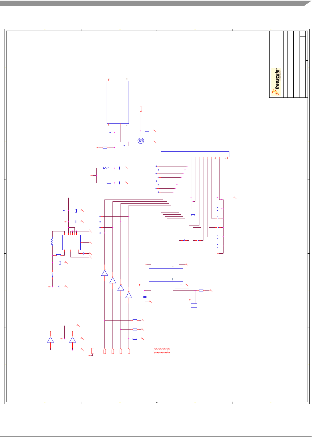
Schematic, Board Layout, and Bill of Material
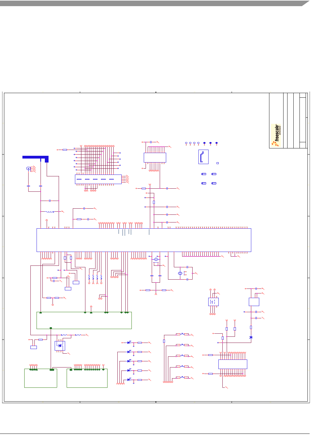
Figure 5-1. Schematic (1 of 4)
5
5
4
4
3
3
2
2
1
1
D D
C C
B B
A A
VCC
VCC
VCC
VCC VCC
VCC
V_MAIN
VCC
VCC
VCC
VCC
VCC
VCC
VCC
LED1
LED2
LED3
LED4
SWITCH4
SWITCH3
SWITCH2
SWITCH1
LED1
LED2
LED4
LED3
SWITCH4
SWITCH3
SWITCH2
SWITCH1
SWITCH5
UART1_CTS
UART1_TX
UART1_RX
UART1_RTS
UART1_TX
UART1_CTS
UART1_RX
UART1_RTS
RESET
RESET
RTCK
RTCK
SWITCH1
SWITCH2
SWITCH3
SWITCH4
SWITCH5
UART2_TX
UART2_RTS
UART2_RX
UART2_CTS
SPI_SCK
SPI_SCK
SPI_MOSI
SPI_SS
SPI_MISO
I2C_SCL
ADC1
ADC2
ADC3ADC4
ADC5
ADC2
ADC3
ADC4
ADC5
UART2_TX
UART2_RX
UART2_CTS
UART2_RTS
I2C_SDA
I2C_SCL
I2C_SDA
SPI_MOSI
SPI_SS
SPI_MISO
TMR1
TMR1
ADC1
SSI_TX
SSI_BITCK
SSI_FSYN
SSI_RX
SSI_TX
SSI_BITCK SSI_FSYN
SSI_RX
SWITCH1 SWITCH5
DAC_OUT
DAC_OUT
TDO
TDI
TCK
TMS
TDI
TDO
TCK
TMS
RESET
TDO
TCK
TMS
TDI
RTCK
MDO0
MDO1
MDO2
MDO3
MDO4
MDO5
MDO6
MDO7
MDO0
MDO1
MDO2
MDO3
MDO4
MDO5
MDO6
MDO7
MCKO
RDY_B
MSEO1_B
MSEO0_B
EVTI_B
EVTO_B
EVTI_B
RDY_B
EVTO_B
MCKO
MSEO1_B
MSEO0_B
VTREF
CLKIN
CLKIN
UART2_CTS
UART2_RTS
TMR1
TMR0
SPI_SS
SPI_MISO
SPI_MOSI
SPI_SCK
ADC2
ADC3
ADC4
ADC5
TMR2
TMR2
TMR0
RESET
Drawing Title:
Size Document Number Rev
Date: Sheet of
Page Title:
ICAP Classification: FCP: FIUO: PUBI:
SOURCE: SCH-23452 PDF: SPF-23452 B1
1322X-NCB
C
Tuesday, May 06, 2008
Main Schematic
36
_X_ ---
---
Drawing Title:
Size Document Number Rev
Date: Sheet of
Page Title:
ICAP Classification: FCP: FIUO: PUBI:
SOURCE: SCH-23452 PDF: SPF-23452 B1
1322X-NCB
C
Tuesday, May 06, 2008
Main Schematic
36
_X_ ---
---
Drawing Title:
Size Document Number Rev
Date: Sheet of
Page Title:
ICAP Classification: FCP: FIUO: PUBI:
SOURCE: SCH-23452 PDF: SPF-23452 B1
1322X-NCB
C
Tuesday, May 06, 2008
Main Schematic
36
_X_ ---
---
GPIO
Pin Header
Push
Buttons
LEDs
RF
JTAG Debug
DBGRQ
DBGACK
nTRST
JTAG RTCK
Enable
Reset
Button
Power ON
Joystick
JTAG RTCK
Disable
Nexus Debug
Note: SWITCH 5 does not have
interrupt capability
Note: SSI_FSYN becomes CLKO
under test conditions
External
Clock
Source
1-2 ADC2_VREFH -> "0"
3-4 ADC2_VREFL -> "1"
Recovery Mode
1.5V
C8
100pF
C8
100pF
R14
1K
R14
1K
X2
32.768kHz
Not Mounted
X2
32.768kHz
Not Mounted
R83
10K
Not Mounted
R83
10K
Not Mounted
TP103TP103
R11
220R
R11
220R
R1
10K
R1
10K
J1
90122-20
J1
90122-20
1
1
3
3
5
5
7
7
9
9
11
11
13
13
15
15
17
17
19
19
22
44
66
88
10 10
12 12
14 14
16 16
18 18
20 20
SW5
DTSM63N
RESET
SW5
DTSM63N
RESET
3
12
4
TP10TP10
Display
Display
TMR1
TMR0
SPI_SS
SPI_MISO
SPI_MOSI
ADC2
ADC3
ADC4
ADC5
TMR2
SPI_SCK
V_DIS
UART2_RTS
UART2_CTS
R13
1K
R13
1K
ZZ4
M3x8.0mm
ZZ4
M3x8.0mm
D3
LHR974
LED3
D3
LHR974
LED3
R6
390R
R6
390R
TP83TP83
REF3
Ref
REF3
Ref
1
1
USB/Power Supply
USB/Power Supply
UART1_CTS
UART1_TX
UART1_RTS
UART1_RX
V_AUD
V_DIS
TP78TP78
R104
10K
R104
10K
C11
1nF
C11
1nF
TP76TP76
R70 0R
Not Mounted
R70 0R
Not Mounted
MH2MH2
1
R64
0R
R64
0R
R5
240R
Not Mounted
R5
240R
Not Mounted
TP70TP70
ZZ3
M3x8.0mm
ZZ3
M3x8.0mm
TP6TP6
TP71TP71
R122 1KR122 1K
C4
27nF
Not Mounted
C4
27nF
Not Mounted
TP45TP45
C49
1uF
C49
1uF
C48
4.7uF
C48
4.7uF
R3
0R
R3
0R
R102
10K
R102
10K
SW2
DTSM63N
SWITCH2
SW2
DTSM63N
SWITCH2
3
12
4
TP8TP8
TP72TP72
C55
10pF
Not Mounted
C55
10pF
Not Mounted
X1
24.00MHz
X1
24.00MHz
C3
1pF
Not Mounted
C3
1pF
Not Mounted
TP80TP80
MH3MH3
1
TP73TP73
ZZ1
Label 1322X-NCB
ZZ1
Label 1322X-NCB
R69 0RR69 0R
D12
MBR0520LT1
D12
MBR0520LT1
L1
3.9nH
Not Mounted
L1
3.9nH
Not Mounted
TP1TP1
R9
390R
R9
390R
C58
10pF
Not Mounted
C58
10pF
Not Mounted
R81
1K
Not Mounted
R81
1K
Not Mounted
R105 0RR105 0R
R123 1KR123 1K
C12
22pF
Not Mounted
C12
22pF
Not Mounted
TP74TP74
R4
0R
Not Mounted
R4
0R
Not Mounted
REF2
Ref
REF2
Ref
1
1
ZZ5
M3x8.0mm
ZZ5
M3x8.0mm
U1
MC13225
U1
MC13225
UART2_RTS
13
EVTI_B 132
MCKO/IO50 131
MSEO0_B 114
EVTO_B 123
RDY_B 122
MSEO1_B 113
VBATT 45
LREG_BK_FB 44
COIL_BK 43
ADC2_VREFL
61 ADC1_VREFL
62
ADC1_VREFH
63
ADC2_VREFH
64
ADC0
1
ADC1
2
ADC2
3
ADC3
4
ADC4
5
ADC5
6
ADC6
7
ADC7_RTCK
8
MDO00 103
MDO01 102
MDO02 112
MDO03 111
MDO04 121
MDO05 120
MDO06 130
MDO07 129
TDI 10
RF_GND 58
TDO 9
UART2_CTS
14
UART2_RX
15
TCK 11
TMS 12
RESETB 51
VREG_ANA 55
XTAL_24_OUT
49
RF_PLL_FLT 46
XTAL_24_IN
50
KBI_0_HST_WK
42
XTAL_32_IN
47
ANT_1 56
XTAL_32_OUT
48
RF_RX_TX 60
ANT_2 57
UART2_TX
16
RX_ON 59
PA_POS 54
PA_NEG 53
TX_ON 52
UART1_RTS
17
UART1_CTS
18
UART1_RX
19 UART1_TX
20
I2C_SDA
21
I2C_SCL
22
TMR3
23
TMR2
24
TMR1
25
TMR0
26
SPI_SCK
27
SPI_MOSI
28
SPI_MISO
29
SPI_SS
30
SSI_BITCK
31
SSI_FSYN
32
SSI_RX
33 SSI_TX
34
KBI_1
41 KBI_2
40 KBI_3
39 KBI_4
38 KBI_5
37 KBI_6
36 KBI_7
35
GND_FLAG_1
75
DIG_REG 124
NVM_REG 133
GND_FLAG_2
76
GND_FLAG_3
77
GND_FLAG_4
78
GND_FLAG_5
79
GND_FLAG_6
84
GND_FLAG_7
85
GND_FLAG_8
86
GND_FLAG_9
87
GND_FLAG_10
88
GND_FLAG_11
93
GND_FLAG_12
94
GND_FLAG_13
95
GND_FLAG_14
96
GND_FLAG_15
97
GND_FLAG_16
104
GND_FLAG_17
105
GND_FLAG_18
106
GND_FLAG_19
115
NC1
65
NC2
66
NC3
67
NC4
68
NC5
69
NC6
70
NC7
71
NC8
72
NC9
73
NC10
74
NC11 80
NC12 81
NC13 82
NC14 83
NC15 89
NC16 90
NC17 91
NC18 92
NC19 98
NC20 99
NC21 100
NC22 101
NC23 107
NC24 108
NC25 109
NC26 110
NC27 116
NC28 117
NC29 118
NC30 119
NC31 125
NC32 126
NC33 127
NC34 128
NC35 134
NC36 135
NC37 136
NC38 137
NC39 138
NC40 139
NC41 140
NC42 141
NC43 142
NC44 143
NC45 144
NC46 145
TP46TP46
R103
10K
R103
10K
Audio
Audio
SCLK
AUDIO_PWM
Din
AUDIO_MIC
SYNC
DAC_OUT
V_AUD
VOL_SCL
VOL_SDA
SW6
SKRHA
SW6
SKRHA
C
3
A
1
Ce
2
D4
Co 5
B6
NC1
7NC2 8
J19
TSM-102-01-L-SV
J19
TSM-102-01-L-SV
11
22
PCB1
JDP7050_3
PCB1
JDP7050_3
TP82TP82
TP9TP9
TP75TP75
J20
TSM-102-01-L-SV
J20
TSM-102-01-L-SV
11
22
ANT1
F_Antenna
ANT1
F_Antenna
R12
100K
R12
100K
D4
LHR974
LED4
D4
LHR974
LED4
SW4
DTSM63N
SWITCH4
SW4
DTSM63N
SWITCH4
3
12
4
ZZ2
M3x8.0mm
ZZ2
M3x8.0mm
J2
90122-26
J2
90122-26
11
33
55
77
99
11 11
13 13
15 15
17 17
19 19
21 21
23 23
25 25
2
2
4
4
6
6
8
8
10
10
12
12
14
14
16
16
18
18
20
20
22
22
24
24
26
26
TP5TP5
R66
0R
Not Mounted
R66
0R
Not Mounted
R8
390R
R8
390R
C1
10pF
Not Mounted
C1
10pF
Not Mounted
C6
100nF
C6
100nF
D2
LHR974
LED2
D2
LHR974
LED2
J11
767054-1
J11
767054-1
1
1
3
3
5
5
7
7
9
9
11
11
13
13
15
15
17
17
19
19
21
21
23
23
25
25
27
27
29
29
31
31
33
33
35
35
37
37
22
44
66
88
10 10
12 12
14 14
16 16
18 18
20 20
22 22
24 24
26 26
28 28
30 30
32 32
34 34
36 36
38 38
GND1
39
GND2
40
GND3
41
GND4
42
GND5
43
R124 1KR124 1K
C9
10nF
Not Mounted
C9
10nF
Not Mounted
C5
180nF
Not Mounted
C5
180nF
Not Mounted
R65
0R
R65
0R
D5
LGR971
POWER
D5
LGR971
POWER
C10
1uF
Not Mounted
C10
1uF
Not Mounted
R121
24.9K
1%
R121
24.9K
1%
C50
100nF
C50
100nF
TP79TP79
TP4TP4
SW1
DTSM63N
SWITCH1
SW1
DTSM63N
SWITCH1
3
12
4
R120
120K
1%
R120
120K
1%
C2
100nF
C2
100nF
J7
SMA
J7
SMA
C7
22pF
Not Mounted
C7
22pF
Not Mounted
SW3
DTSM63N
SWITCH3
SW3
DTSM63N
SWITCH3
3
12
4
REF1
Ref
REF1
Ref
1
1
R125 1KR125 1K
TP7TP7
U17
LM285M
U17
LM285M
1
1
2
2
3
3
4
455
66
77
88
J18
TSM-102-01-L-SV
J18
TSM-102-01-L-SV
11
22
MH4MH4
1
TP44TP44
R82
1K
Not Mounted
R82
1K
Not Mounted
MH1MH1
1
R7
390R
R7
390R
D1
LHR974
LED1
D1
LHR974
LED1
TP11TP11
C54
10pF
C54
10pF
TP77TP77
TP3TP3
TP81TP81
U12
LT1129CST-3.3
U12
LT1129CST-3.3
Vin 1
Vout
3
GND1 2
GND2 4
Schematic, Board Layout, and Bill of Material
1322x Network Node Reference Manual, Rev. 1.1
5-2 Freescale Semiconductor
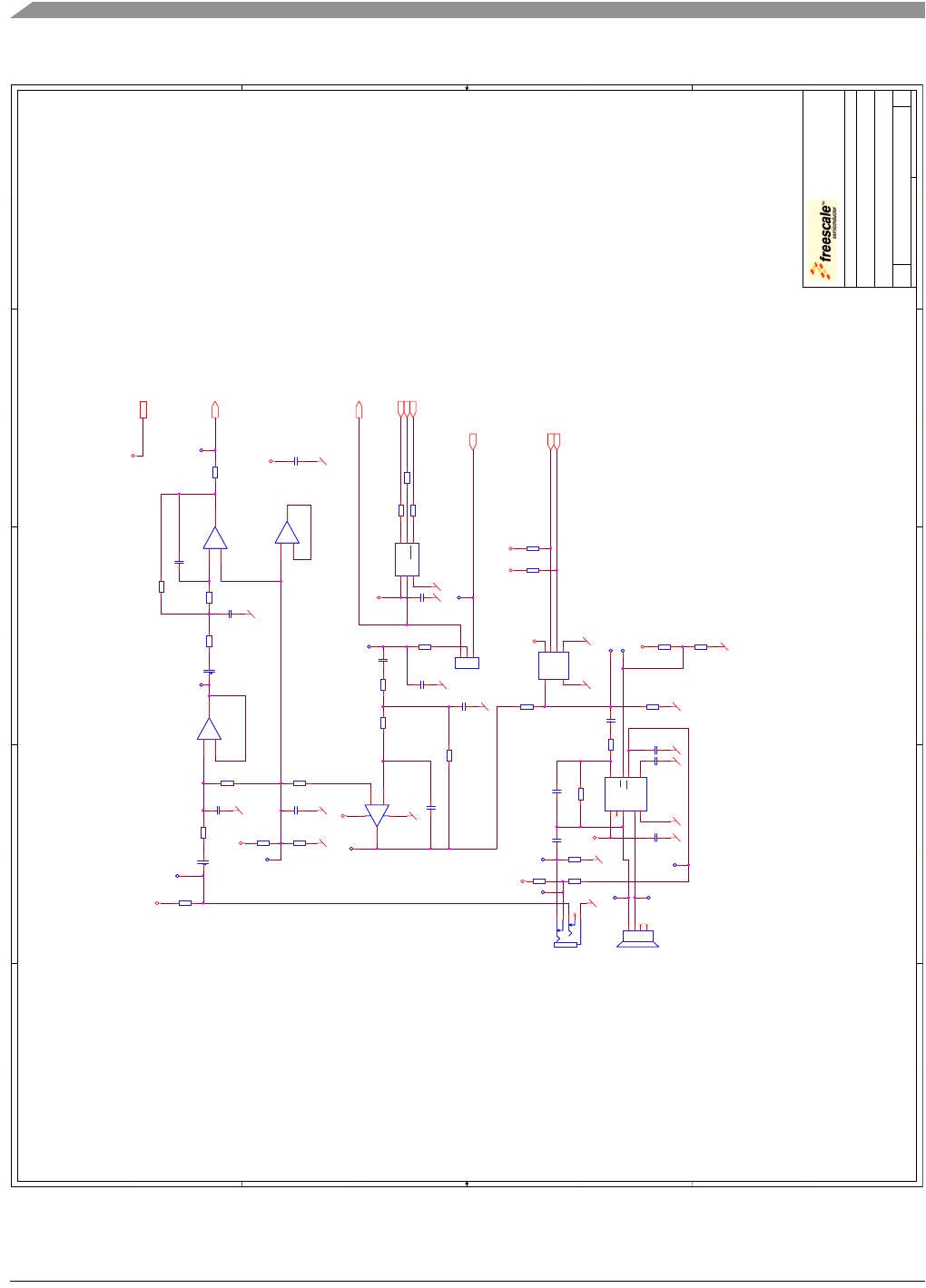
Figure 5-2. Schematic (2 of 4)
5
5
4
4
3
3
2
2
1
1
D D
C C
B B
A A
AUDIO_MIC
Din
SCLK
AUDIO_PWM
SYNC
DAC_OUT
V_AUD
VOL_SDA
VOL_SCL
V_AUD
V_AUD
V_AUD
V_AUD
V_AUD
V_AUD
VCC VCC
V_AUD
V_AUD
V_AUD
V_AUD
Drawing Title:
Size Document Number Rev
Date: Sheet of
Page Title:
ICAP Classification: FCP: FIUO: PUBI:
SOURCE: SCH-23452 PDF: SPF-23452 B1
1322X-NCB
C
Tuesday, May 06, 2008
Audio Schematic
46
_X_ ---
---
Drawing Title:
Size Document Number Rev
Date: Sheet of
Page Title:
ICAP Classification: FCP: FIUO: PUBI:
SOURCE: SCH-23452 PDF: SPF-23452 B1
1322X-NCB
C
Tuesday, May 06, 2008
Audio Schematic
46
_X_ ---
---
Drawing Title:
Size Document Number Rev
Date: Sheet of
Page Title:
ICAP Classification: FCP: FIUO: PUBI:
SOURCE: SCH-23452 PDF: SPF-23452 B1
1322X-NCB
C
Tuesday, May 06, 2008
Audio Schematic
46
_X_ ---
---
Audio Amplifier
Audio DAC
Audio Amp
Enable
Audio Amp
Disable
Audio Select
1-2 DAC
3-2 PWM
Audio Filter
Mic. Amplifier/Anti-alias Filter
Mic. Biasing
R26
100K
R26
100K
R15
10K
R15
10K
J10
TSM-103-01-L-SV
J10
TSM-103-01-L-SV
11
22
33
BUZ1
NDT-03C
BUZ1
NDT-03C
+1
-2
NC1 3
NC2 4
R87
10K
R87
10K
R24
100K
R24
100K
C46
270pF
C46
270pF
C22
100nF
C22
100nF
C20
47pF
C20
47pF
+
-
U2B
MC33204DTBG
+
-
U2B
MC33204DTBG
5
6
7
R84
0R
R84
0R
C16
100pF
C16
100pF
R109 0RR109 0R
TP25TP25
R29
47K
R29
47K
R86
1.8K
R86
1.8K
+
-
U2D
MC33204DTBG
+
-
U2D
MC33204DTBG
12
13
14
U4
DAC101S101
U4
DAC101S101
SCLK 5
VDD
3
GND
2SYNC 6
Din 4
Vout
1
C15
10UF
C15
10UF
C25
1uF
C25
1uF
R67
27K
R67
27K
TP18TP18
R25
1K
R25
1K
R34
0R
Not Mounted
R34
0R
Not Mounted
C30
22nF
C30
22nF
TP24TP24
R20
200K
R20
200K
R33
0R
R33
0R
C44
1uF
C44
1uF
R23
100K
R23
100K
R85
11K
R85
11K
R106
4.7K
R106
4.7K
R30
220R
R30
220R
R56
4.7K
R56
4.7K
TP49TP49
R32
0R
Not Mounted
R32
0R
Not Mounted
C29
4.7nF
C29
4.7nF
TP48TP48
TP23TP23
C45
220nF
C45
220nF
C19
22uF
C19
22uF
C47
3.3nF
C47
3.3nF
TP51TP51
C24
1uF
C24
1uF
C28
47nF
C28
47nF
U6
NCP4896
U6
NCP4896
INM C1
SE/BTL A1
VP1
B1
GND
B3 OUTB
A3
NC
B2
OUTA
C3
BYP A2
SD C2
U13
MAX5434
U13
MAX5434
VCC 1
GND 2
SDA 4
SCL 3
L
6
W
5
TP20TP20
+
-
U2A
MC33204DTBG
+
-
U2A
MC33204DTBG
3
2
1
411
R57
4.7K
R57
4.7K
TP16TP16
R110 0RR110 0R
R88
51K
R88
51K
C21
100nF
C21
100nF
C13
100nF
C13
100nF
R60
8.2K
R60
8.2K
J12
STX-2550-5NTR
J12
STX-2550-5NTR
1
3
5
4
2
+
-
U2C
MC33204DTBG
+
-
U2C
MC33204DTBG
10
8
9
TP15TP15
C14
10UF
C14
10UF
TP19TP19
R58
27K
R58
27K
TP50TP50
R61
13K
R61
13K
R107
4.7K
R107
4.7K
R111 0RR111 0R
TP22TP22
TP17TP17
R59
27K
R59
27K
C27
100nF
C27
100nF
Schematic, Board Layout, and Bill of Material
1322x Network Node Reference Manual, Rev. 1.1
Freescale Semiconductor 5-3
Figure 5-3. Schematic (3 of 4)
5
5
4
4
3
3
2
2
1
1
D D
C C
B B
A A
P/S
IRS
LED_PWM
RESN
VDD
D4
D3
D2
D1
D0
V2
V3
V4
VOUT
CAP3-
CAP2+
CAP2-
CAP1-
CAP1+
V1
D5
D6
D7
GND
RDN
CSN
A0
WRN
V5
ADC4
ADC3
SPI_MOSI
SPI_MISO
SPI_SS
V_DIS
UART2_CTS
TMR1
TMR0
UART2_RTS
ADC5
TMR2
ADC2
SPI_SCK
5V_LCD
5V_LCD
5V_LCD
V_DIS
5V_LCD
V_DIS
5V_LCD
V_DIS
V_DIS
V_DIS
Drawing Title:
Size Document Number Rev
Date: Sheet of
Page Title:
ICAP Classification: FCP: FIUO: PUBI:
SOURCE: SCH-23452 PDF: SPF-23452 B1
1322X-NCB
C
Tuesday, May 06, 2008
Display Schematic
56
_X_ ---
---
Drawing Title:
Size Document Number Rev
Date: Sheet of
Page Title:
ICAP Classification: FCP: FIUO: PUBI:
SOURCE: SCH-23452 PDF: SPF-23452 B1
1322X-NCB
C
Tuesday, May 06, 2008
Display Schematic
56
_X_ ---
---
Drawing Title:
Size Document Number Rev
Date: Sheet of
Page Title:
ICAP Classification: FCP: FIUO: PUBI:
SOURCE: SCH-23452 PDF: SPF-23452 B1
1322X-NCB
C
Tuesday, May 06, 2008
Display Schematic
56
_X_ ---
---
U14B
74HCT04A
U14B
74HCT04A
3 4
L3
22uH
L3
22uH
R101
100K
R101
100K
C75
4.7UF
USE MURATA PART
C75
4.7UF
USE MURATA PART
U14C
74HCT04A
U14C
74HCT04A
5 6
+
C60
47uF
+
C60
47uF
R96
200R
R96
200R
TP96TP96
C74
10nF
C74
10nF
TP91TP91
TP101TP101
TP102TP102
+
C70
1uF
+
C70
1uF
R100
100K
R100
100K
J13
6210_30_smd
LCD CONNECTOR
J13
6210_30_smd
LCD CONNECTOR
1
1
2
2
3
3
4
4
5
5
6
6
7
7
8
8
9
9
10
10
11
11
12
12
13
13
14
14
15
15
16
16
17
17
18
18
19
19
20
20
21
21
22
22
23
23
24
24
25
25
26
26
27
27
28
28
29
29
30
30
31
31
32
32
TP88TP88
TP94TP94
TP89TP89
U14D
74HCT04A
U14D
74HCT04A
13 12
TP99TP99
R98
100K
R98
100K
TP90TP90
C72
100nF
C72
100nF
C62
10nF
C62
10nF
U14A
74HCT04A
U14A
74HCT04A
1 2
714
+
C67
1uF
+
C67
1uF
R99
100K
R99
100K
TP97TP97
U15
MAX1676EUB+
U15
MAX1676EUB+
GND
8
LX 9
SHDN 6
FB 1
BATT
7
LBO 3
REF
5
OUT 10
CLSEL 4
LBI
2
G
D
S
Q2
ZVN3320F
G
D
S
Q2
ZVN3320F
+
C63
4.7uF
+
C63
4.7uF
R90
47 OHM
USE VISHAY PART
R90
47 OHM
USE VISHAY PART
U14E
74HCT04A
U14E
74HCT04A
11 10
+
C66
1uF
+
C66
1uF
128x64
Monochrome-Graphic
Liquid Crystal Display
D11
F-51553GNBJ-LW-AB
128x64
Monochrome-Graphic
Liquid Crystal Display
D11
F-51553GNBJ-LW-AB
01
302 4
03
504 6
+ Anode
1
- Cathode
2
C59
100nF
C59
100nF
TP95TP95
+
C68
1uF
+
C68
1uF
R44
7.15 OHM
R44
7.15 OHM
TP100TP100
U14F
74HCT04A
U14F
74HCT04A
9 8
C61
100nF
C61
100nF
R91
0R
Not Mounted
R91
0R
Not Mounted
TP93TP93
U16
MC74LVXC3245DT
U16
MC74LVXC3245DT
A1
4
A2
5
A3
6
A4
7
A5
8
A6
9
A7
10
A0
3
OE
22
T/R
2
B1 20
B2 19
B3 18
B4 17
B5 16
B6 15
B7 14
B0 21
VCCB 24
GND 13
GND
11
GND
12
VCCA
1
NC 23
R89
10K
R89
10K
+
C73
47uF
+
C73
47uF
+
C64
4.7uF
+
C64
4.7uF
TP98TP98
R97
100K
R97
100K
C71
100nF
C71
100nF
+
C65
4.7uF
+
C65
4.7uF
TP92TP92
+
C69
1uF
+
C69
1uF
J14
TSM-102-01-L-SV
J14
TSM-102-01-L-SV
11
22
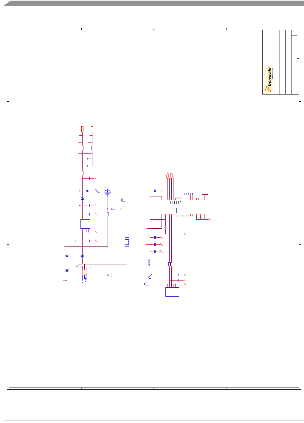
Schematic, Board Layout, and Bill of Material
1322x Network Node Reference Manual, Rev. 1.1
5-4 Freescale Semiconductor
Figure 5-4. Schematic (4 of 4)
5
5
4
4
3
3
2
2
1
1
D D
C C
B B
A A
UART1_TX
UART1_CTS
UART1_RX
UART1_RTS
V_AUD
V_DIS
V_USB
V_USB
V_AUD
VCC
V_MAIN
V_DIS
Drawing Title:
Size Document Number Rev
Date: Sheet of
Page Title:
ICAP Classification: FCP: FIUO: PUBI:
SOURCE: SCH-23452 PDF: SPF-23452 B1
1322X-NCB
C
Tuesday, May 06, 2008
USB/Power Supply Schematic
66
_X_ ---
---
Drawing Title:
Size Document Number Rev
Date: Sheet of
Page Title:
ICAP Classification: FCP: FIUO: PUBI:
SOURCE: SCH-23452 PDF: SPF-23452 B1
1322X-NCB
C
Tuesday, May 06, 2008
USB/Power Supply Schematic
66
_X_ ---
---
Drawing Title:
Size Document Number Rev
Date: Sheet of
Page Title:
ICAP Classification: FCP: FIUO: PUBI:
SOURCE: SCH-23452 PDF: SPF-23452 B1
1322X-NCB
C
Tuesday, May 06, 2008
USB/Power Supply Schematic
66
_X_ ---
---
USB Interface
Power Management Power Measurement
2xAA Cells
R68
0R
R68
0R
U10
FT232R
U10
FT232R
TxD 30
RxD 2
RTS 32
CTS 8
DTR 31
DSR 6
DCD 7
RI 3
AGND 24
GND1
4
GND2
17
VCC
19 VCCIO 1
3V3OUT
16
USBDM
15
USBDP
14
RESET
18
OSCI
27
OSCO
28
EP 33
CBUS4 9
CBUS3 11
CBUS2 10
CBUS1 21
CBUS0 22
NC1
5
NC2
12
NC3
13
GND3
20
NC4
23
NC5 25
NC6 29
TEST
26
RT1
500mA
RT1
500mA
R51 0RR51 0R
TP41TP41
C43
15pF
C43
15pF
D8
MBR0520LT1
D8
MBR0520LT1
TP38TP38
TP32TP32
C35
100nF
C35
100nF
SW7-1
MFP461N-RA
SW7-1
MFP461N-RA
1
2
3
D6
MBR0520LT1
D6
MBR0520LT1
R80
0R
R80
0R
TP40TP40
J5
DJ-005
J5
DJ-005
1
3
2
J6
USB-B
J6
USB-B
VUSB 1
Data- 2
Data+ 3
GND 4
SHIELD1 5
SHIELD2 6
D7
MBR0520LT1
D7
MBR0520LT1
R42
100K
R42
100K
C42
15pF
C42
15pF
C41 100nFC41 100nF
C40
100nF
C40
100nF
TP28TP28
R43
0R
R43
0R
RT2
500mA
RT2
500mA
TP29TP29
SW7-3
MFP461N-RA
SW7-3
MFP461N-RA
7
8
9
C38
100nF
C38
100nF
TP60TP60
L2
60OHM
L2
60OHM
1 2
D10
MBR0520LT1
D10
MBR0520LT1
TP26TP26
TP33TP33
Q1
ZXM61P02F
Q1
ZXM61P02F
R50 0RR50 0R
D9
MBR0520LT1
D9
MBR0520LT1
BC1
2462
BC1
2462
+1
-
2
U9
LT1129CST-3.3
U9
LT1129CST-3.3
Vin
1Vout 3
GND1
2
GND2
4
TP43TP43
TP39TP39
C56
10nF
C56
10nF
C36
4.7uF
C36
4.7uF
TP47TP47
SW7-4
MFP461N-RA
SW7-4
MFP461N-RA
10
11
12
C37
4.7uF
C37
4.7uF
TP42TP42
R40
10K
R40
10K
SW7-2
MFP461N-RA
SW7-2
MFP461N-RA
4
5
6
C34
1uF
C34
1uF
C57
4.7uF
C57
4.7uF
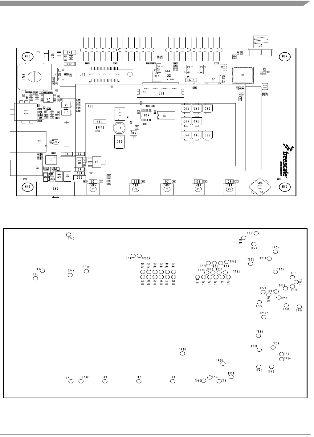
Schematic, Board Layout, and Bill of Material
1322x Network Node Reference Manual, Rev. 1.1
Freescale Semiconductor 5-5
Figure 5-5. Network Node PCB Component Location (Top View)
Figure 5-6. Network Node PCB Test Points (Bottom View)
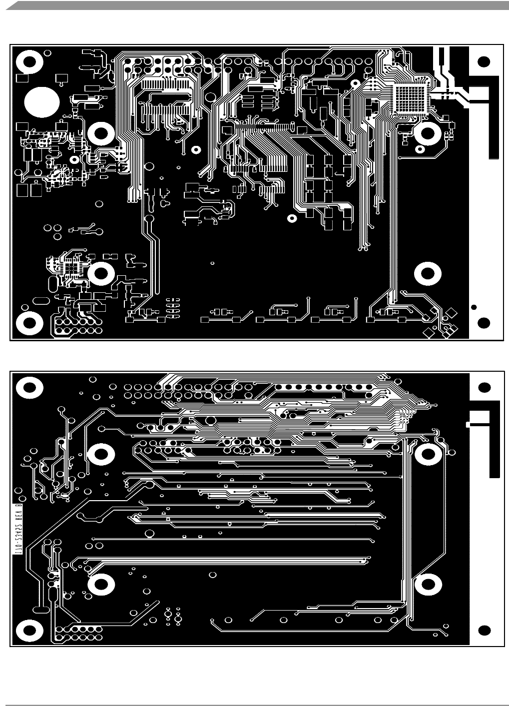
Schematic, Board Layout, and Bill of Material
1322x Network Node Reference Manual, Rev. 1.1
5-6 Freescale Semiconductor
Figure 5-7. Network Node PCB Layout (Top View)
Figure 5-8. Network Node PCB Layout (Bottom View)

Schematic, Board Layout, and Bill of Material
1322x Network Node Reference Manual, Rev. 1.1
Freescale Semiconductor 5-7
Table 5-1. Bill of Materials
Qty Part
Reference Description Value Voltage Tolerance Manufacturer Manufacturer Part
Number
1 ANT1 F_Antenna PCB F
Antenna
Not A Part NOT A PART
1 BUZ1 SMD Speaker NDT-03C Star Micronics NDT-03C
1 C54 Ceramic Capacitor C0G 10pF 50V 5% Murata GRM1555C1H100JZ01
0 C1,C55,C58 Ceramic Capacitor C0G 10pF 50V 5% Murata GRM1555C1H100JZ01
3 C24,C25,C44 Ceramic Capacitor X5R 1uF 6.3V 10% Murata GRM155R60J105KE19B
0 C10 Ceramic Capacitor X5R 1uF 6.3V 10% Murata GRM155R60J105KE19B
1 C11 Ceramic Capacitor X7R 1nF 50V 10% Murata GRM155R71H102KA01D
2 C14,C15 CAP CER 10UF 6.3V
20% X5R 0603
10uF 6.3V 20% Panasonic ECJ1VB0J106M
1 C19 Ceramic Capacitor for
smoothing X5R
10uF 10V 10% Murata GRM21BR61J106KE19L
15 C2,C6,C13,C
21,C22,C27,
C35,C38,C40
,C41,C50,C5
9,C61,C71,C
72
Ceramic Capacitor X5R 100nF 10V 10% Murata GRM155R61A104KA01D
1 C20 Ceramic Capacitor C0G 47pF 50V 5% Kemet C0402C470J5GAC
1 C28 Ceramic Capacitor X5R 47nF 10V 10% Panasonic-ecg ECJ-0EB1A473K
1 C29 Ceramic Capacitor X7R 4.7nF 25V 10% Murata GRM155R71E472KA01
1 C30 Ceramic Capacitor X7R 22nF 25V 10% Murata GRM155R71E223KA61D
0 C3 Ceramic Capacitor C0G 1pF 50V 0.25pF Murata GRM1555C1H1R0CZ01D
2 C34,C49 Ceramic Multilayer
Capacitor X7R NoPb
1uF 16V 15% Murata GRM21BR71C105
3 C36,C37,C48 Ceramic Multilayer
Capacitor X5R
4.7uF 16V 15% Phycomp 2222 781 13672
0 C4 Ceramic Multilayer
Capacitor X7R
27nF 10V 5% Vishay VJ0402Y273JXQCW1BC
2 C42,C43 Ceramic Capacitor C0G 15pF 50V 5% Murata GRM1555C1H150JZ01J
1 C45 Ceramic Capacitor X7R 220nF 10V 10% Murata GRM188R71A224KA01
1 C46 Ceramic Capacitor C0G 270pF 50V 5% Murata GRM1555C1H271JA01
1 C47 Ceramic Capacitor C0G 3.3nF 50V 15% Murata GRM155R71H332KA01
0 C5 Ceramic Multilayer
Capacitor X7R
180nF 16V 5% Vishay VJ0603Y184JXJCW1BC
1 C57 Ceramic Multilayer
Capacitor X5R
4.7uF 10V 10% Murata GRM219R61A475KE34D

Schematic, Board Layout, and Bill of Material
1322x Network Node Reference Manual, Rev. 1.1
5-8 Freescale Semiconductor
2 C60,C73 Low ESR Tantal
Capacitor
47uF 16V +/-10% Avx TPSD476K016R150
3 C63,C64,C65 Aluminum Electrolytic
Capacitor low ESR
CV-GX
4.7uF 35V 20% Sanyo 35CV4.7GX
5 C66,C67,C68
,C69,C70
Aluminum Electrolytic
Capacitor
1uF 50V 20% Nic
Components
NACE 1R0 M 50V 4x5,5
TR13
0 C7,C12 Ceramic Capacitor C0G 22pF 50V 5% Murata GRM1555C1H220JZ01J
1 C75 CAP CER 4.7UF 6.3V
10% X5R 0603
4.7uF 6.3V 10% Venkel
Company
C0603X5R6R3-475KNE
2 C8,16 Ceramic Capacitor C0G 100pF 50V 5% Murata GRM1555C1H101JZ01
3 C56,C62,C74 Ceramic Capacitor X7R 10nF 25V 10% Murata GRM155R71E103KA01D
0 C9 Ceramic Capacitor X7R 10nF 25V 10% Murata GRM155R71E103KA01D
4 D1,D2,D3,D4 SMD Red topled LHR974 Osram Q62702P5182
1 D5 SMD Green topled LGR971 Osram Q65110P5179
6 D6,D7,D8,D9,
D10,D12
SMD Power Schottky
Rectifier
MBR0520
LT1
20V On
Semiconductor
MBR0520LT1G
1 J10 Single Row Straight Pin
Header SMD
TSM-103-
01-L-SV
Samtec TSM-103-01-L-SV
1 J11 Mictor, Centerline
Matched Impedance
Connector
767054-1 Amp 767054-1
1 J12 2.5mm Audio stereo jack
with switch
STX-2550
-5NTR
Kycon STX-2550-5NTR
1 J13 FFC Right Angle Dip Zif
30 pin Connector
6210_30_
smd
Avx 08 6210 030 340 800
4J14,
J18,J19,J20
Single Row Straight Pin
Header SMD
TSM-102-
01-L-SV
Samtec TSM-102-01-L-SV
0 J18,J19,J20 HDR 1X2 SMT 78.7MIL
SP 235H AU
HDR_1X2 Samtec TMM-102-01-S-S-SM
0 L1 HF Chip coil 3.9nH 5% Murata LQG15HS3N9S02D
1 L2 Chip Ferrite Bead 500mA Murata BLM11P600Sxx
1 L3 SMD power inductor 22uH 20% Coilcraft DO1608C-223LC
1 Q1 P-channel MOSFET ZXM61P0
2F
20V Zetex ZXM61P02F
1 Q2 N-Chanel Enhancement
MOSFET
ZVN3320
F
200V Zetex ZVN3320FTA
Table 5-1. Bill of Materials
Qty Part
Reference Description Value Voltage Tolerance Manufacturer Manufacturer Part
Number

Schematic, Board Layout, and Bill of Material
1322x Network Node Reference Manual, Rev. 1.1
Freescale Semiconductor 5-9
15 R3,R33,R43,
R50,R51,R64
,R65,R68,R6
9,R80,R84,R
105,R109,R1
10,R111
Fixed resistor RC31 0R 50V 2% Philips 2322 705 91002
0 R4,R32,R34,
R66,R70,R91
Fixed resistor RC31 0R 50V 2% Philips 2322 705 91002
2 R11,R30 Fixed resistor RC31 220R 50V 2% Philips 2322 705 50221
10 R12,R23,R24
,R26,R42,R9
7,R98,R99,R
100,R101
Fixed resistor RC31 100K 50V 2% Philips 2322 705 50104
3 R13,R14,R25 Fixed resistor RC31 1K 50V 2% Philips 2322 705 50102
0 R81,R82 Fixed resistor RC31 1K 50V 2% Philips 2322 705 50102
4 R56,R57,R10
6,R107
Fixed resistor RC31 4.7K 50V 2% Philips 2322 705 50472
9 R1,R15,R40,
R44,R87,R89
,R102,R103,
R104
Fixed resistor RC31 10K 50V 2% Philips 2322 705 50103
1 R44 Fixed resistor RC31 7R15 1% Koa Speer RK73H1ETTP7R15F
0 R83 Fixed resistor RC31 10K 50V 2% Philips 2322 705 50103
1 R20 Fixed resistor RC31 200K 50V 2% Yageo America RC0402JR-07200KL
1 R29 Fixed resistor RC31 47K 50V 2% Philips 2322 705 50473
0 R5 Fixed resistor RC31 240R 50V 2% Philips 2322 705 50241
3 R58,R59,R67 Fixed resistor RC31 27K 50V 2% Philips 2322 705 50273
4 R6,R7,R8,R9 Fixed resistor RC31 390R 50V 2% Philips 2322 705 50391
1 R60 Fixed resistor RC31 8.2K 50V 2% Philips 2322 705 50822
1 R61 Fixed resistor RC31 13K 50V 2% Philips 2322 705 50133
1 R85 Fixed resistor RC32 11K 50V Koa Speer RK73H1ETTP1102F
1 R86 Fixed resistor RC33 1.8K 50V Koa Speer RK73H1ETTP1801F
1 R88 Fixed resistor RC34 51K 200V Koa Speer RK73H1ETTP5102F
1 R96 RESISTOR 200 OHM Vishay/dale CRCW0402200RJNED
1 R90 RES MF 47 OHM 1/4W
5% 1206
47 OHM 5% Bourns CR1206-JW-470ELF
1 R120 RES MF 120K 1/16W
1% 0402
120K 1% Koa Speer RK73H1ETTP1203F
Table 5-1. Bill of Materials
Qty Part
Reference Description Value Voltage Tolerance Manufacturer Manufacturer Part
Number

Schematic, Board Layout, and Bill of Material
1322x Network Node Reference Manual, Rev. 1.1
5-10 Freescale Semiconductor
1 R121 RES MF 24.9K 1/16W
1% 0402
24.9K 1% Koa Speer RK73H1ETTP2492F
4 R122,R123,R
124,R125
RES MF 1.0K 1/16W 5%
0402
1K 5% Vishay
Intertechnology
CRCW04021K00JNED
2 RT1,RT2 Polyswitch Overcurrent
Protection Device
500mA 13.2V Tyco
Electronics
microSMD050F
5SW1,SW2,S
W3,SW4,SW
5
SMD Tact Switch 2.6N
(7.0mm)
DTSM63
N
Diptronic DTSM-63N-V-B
1 SW6 4-directional TACT
switch with center push
SMD
SKRHA Alps SKRHAAE010
1 SW7 Miniature Slide Switch 4
pole
MFP461N
-RA
Knitter-switch MFP461N-RA
1 U1 ZigBee Wireless
Transceiver and ARM7
processor
MC13225 Freescale MC13225
1 U10 USB UART, PB-free FT232R Ftdi FT232RQ
1 U13 Digitally Controled
Potentiometer, 50Kohm
MAX5434 Maxim MAX5434LEZT+T
1 U14 Hex inverter 74HCT04
A
On
Semiconductor
MC74HCT04ADTR2G
1 U15 Low supply current
Step-up DC-DC
Converter with shutdown
MAX1676 Maxim MAX1676EUB+-ND
1 U16 Low Voltage CMOS Octal
Bidirectional Transceiver
74LCX24
5
On
Semiconductor
MC74LVXC3245DTG
1 U2 Dual Low voltage
Op-Amp
MC33202 On
Semiconductor
MC33204DTBG
1 U4 10-bit Low Power DAC
with rail to rail output
DAC101S
101
National
Semiconductor
DAC101S101CIMK-NoPB
1 U6 Audio class AB amplifier,
1,0W
NCP4896 On
Semiconductor
NCP4896FCT1G
2 U9,U12 LDO voltage regulator
3V3
LT1129CS
T-3.3
Linear
Technology
LT1129CST-3.3
1 U17 IC VREG ADJ 1.24-5.3V
20MA SOIC8
LM285M National
Semiconductor
LM285M/NOPB
1 X1 Crystal SMD 24.00MHz +-10ppm Ndk NX3225SA-24MHz (for
OA/AV and Blootooth) /
S1-3085-1510-9
Table 5-1. Bill of Materials
Qty Part
Reference Description Value Voltage Tolerance Manufacturer Manufacturer Part
Number
Schematic, Board Layout, and Bill of Material
1322x Network Node Reference Manual, Rev. 1.1
Freescale Semiconductor 5-11
0 X2 Crystal SMD 32.768kH
z
+-20ppm Abracon ABS25-32.768-12.5-2-T
1 D11 128x64 pixel
monochrome display w.
LED backlight
F-51553G
NBJ-LW-A
B
Optrex F-51553GNBJ-LW-AEN
1 BC1 PCB Battery Holder
2xAA
2462 Keystone 2462
1 J1 Dual Row Right Angle pin
header 0.38um gold
90122-20 Molex 90122-0770
1 J2 Dual Row Right Angle pin
header 0.38um gold
90122-26 Molex 90122-0773
1 J5 DC Power Jack PCB,
2mm
DJ-005 Taitek 2DC-0005-D100
1 J6 USB-series "B"
receptacle
USB-B Amp 292304-1
1 J7 Straight SMA Receptacle
for PCB edge mounting
(0.79mm PCB)
SMA Johnson
Components
142-0701-881
Table 5-1. Bill of Materials
Qty Part
Reference Description Value Voltage Tolerance Manufacturer Manufacturer Part
Number

Schematic, Board Layout, and Bill of Material
1322x Network Node Reference Manual, Rev. 1.1
5-12 Freescale Semiconductor