Freescale Semiconductor 1323X-MRB Developer Board User Manual 1323xDHRM
Freescale Semiconductor, Inc. Developer Board 1323xDHRM
Contents
- 1. User Manual 1
- 2. User Manual 2
User Manual 2

1323x Remote Control Motherboard
1323x Development Hardware Reference Manual, Rev. 1.0
Freescale Semiconductor 4-7
Again referring to Figure 4-3, a number of zero-ohm resistors are provided to isolate different circuits and
to allow current measurement:
• VCC (main 1323x-RCM supply) - resistor R35
• V_LED (all LEDs supply) - resistor R36
• V_TPD (touchpad supply) - resistor R37
• V_ACC (accelerometer supply) - resistor R40
• V_BUZ (buzzer supply) - resistor R42
• V_MRB (1323x-MRB supply) - resistor R43
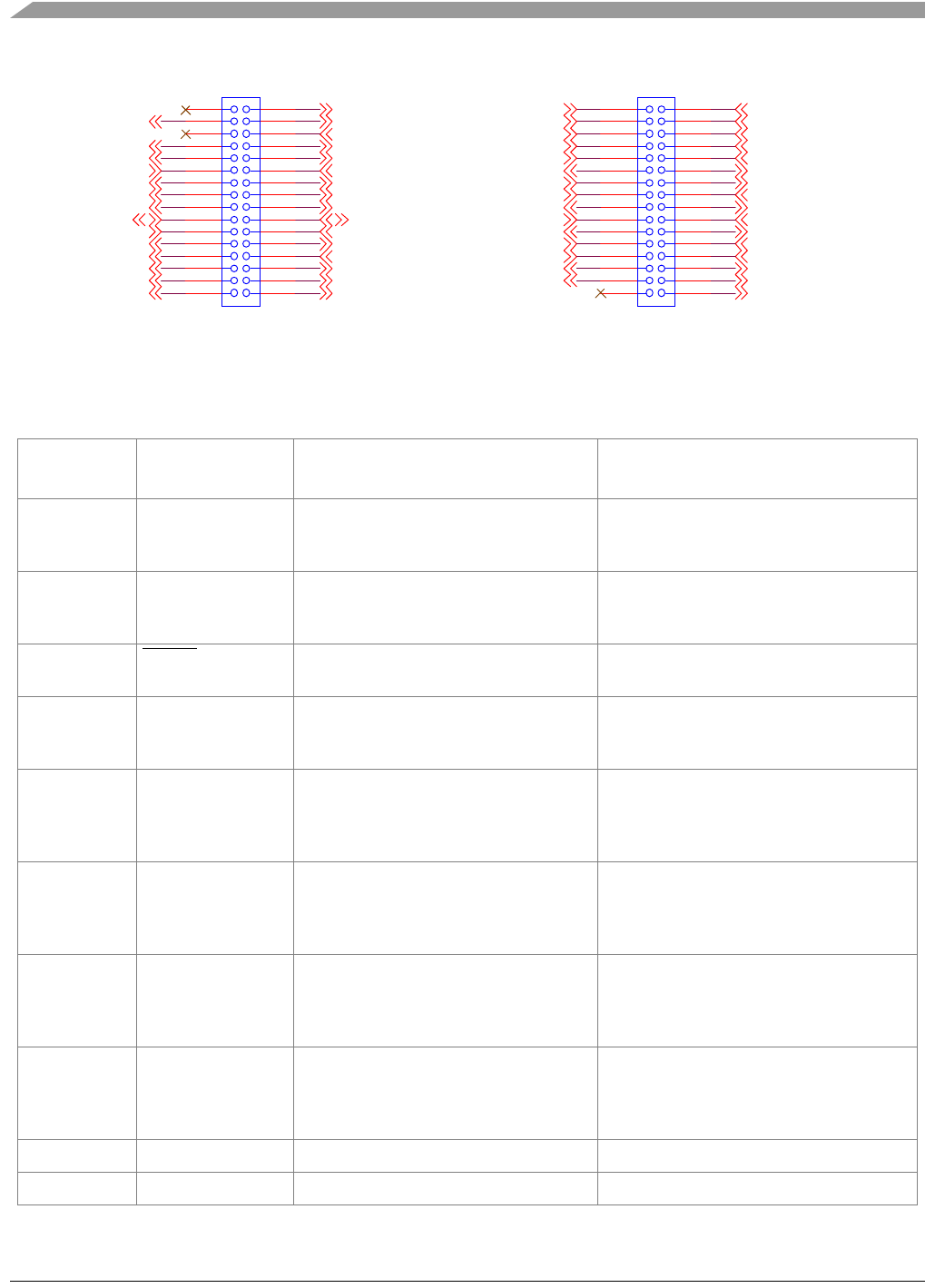
4.2.2 GPIO Connection to 1323x-MRB
IO Connectors J8 and J9 (see Figure 4-1) are receptacles that accept the 1323x-MRB pin headers to mount
the daughter card. Figure 2-1 shows the 1323x-RCM with the 1323x-MRB mounted. Receptacles J8 and
J9 connect to the MC13233 GPIO.
To provide better access and versatility to the GPIO, a secondary set of pin headers P1 and P2 is connected
in series with the IO signals:
• Jumpers must be installed on P1 and P2 to connect 1323x-RCM peripherals and functions
• The pin headers provide direct access for connecting custom circuitry to the GPIO
• Power and ground to primary connectors J8 and J9 are not enabled though the pin headers
Figure 4-4 shows IO Header P1 andP2 pin mapping.
External DC Supply 1x2 Pin Header
J14
2.3 V - 6 V The input voltage range is determined by the U8 regulator
and the diode isolation circuit
Two AA Batteries Battery Holder 2.0 V - 3.1 V1 • The input voltage range reflects the usable range of
alkaline cells and the voltage drop incurred by the diode
isolation circuit.
• The battery source is disabled if another source is
connected
1The minimum operating battery voltage is determined by use model, see Note, Section 4.2.1, “Power Management”
Table 4-2. 1323x-RCM Voltage Sources
Source Connector Input Voltage
Range Description
1323x Remote Control Motherboard
1323x Development Hardware Reference Manual, Rev. 1.0
4-8 Freescale Semiconductor
Figure 4-4. 1323x-RCM IO Connector J8 and J9 Pin Mapping
Table 4-3 list the P1 and P2 pin header function as it relates to the MC13233.
Table 4-3. 1323x-RCM P1 and P2 Pin Header Function Description
1323x-REM
Header Pins
MC13233
Signal Name Description 1323x-REM Application / Notes
P1-27, P1-28 PTA0/XTAL_32K Port A Bit 2 / 32.768 kHz oscillator output • Drives LED1; jumper required
• 32.768 kHz oscillator can be enabled on
MRB
P1-25, P1-26 PTA1/EXTAL_32K Port A Bit 3 / 32.768 kHz oscillator input • Drives Buzzer; jumper required
• 32.768 kHz oscillator can be enabled on
MRB
P1-13, P1-14 RESET Device asynchronous hardware reset.
Active low. Onboard Pullup
• Drives touchpad reset; jumper required
• Reset signal driven from MRB
P1-29, P1-30 PTA2 Port A Bit 2. Onboard pull-down for TM • Drive LCD_CTL0; jumper required
• Application is LCD enable clock
• TM enable
P2-13, P2-14 PTA3/IRQ Port A Bit 3 / IRQ. • Used; jumper required
• Provides interrupt request input IRQ
(active low) from accelerometer and
touchpad
P2-17, P2-18 PTA4/
XTAL_32KOUT
Port A Bit 4 / Buffered 32.768 kHz clock
output
• Drives LED2; jumper required
• Optional 32.768 kHz output clock for
measuring reference oscillator accuracy
(ppm)
P1-19, P1-20 PTA5/SDA Port A Bit 5 / IIC Bus data • Used; jumper required
• Connects to accelerometer
• Defaults to open drain for IIC
• Pullup on MRB
P1-23, P1-24 PTA6/SCL Port A Bit 6 / IIC Bus clock • Used; jumper required
• Connects to accelerometer
• Defaults to open drain for IIC
• Pullup on MRB
P2-1, P2-2 PTB0/KBI1P0 Port B Bit 0 / KBI1 Input Bit 0 RCM switch matrix; jumper required
P2-3, P2-4 PTB1/KBI1P1 Port B Bit 1 / KBI1 Input Bit 1 RCM switch matrix; jumper required
MRB-SPI _MI SO
MRB-U AR T_TXD
MRB- KBI 2P2
MRB- KBI 2P0
MRB-SPI_SS
MRB-SPI _MOSI
MRB-PTA2/LCD_CTL0LCD_CTL0
MRB- PTD1/ TPM1
MRB- KBI 1P1
MRB- KBI 1P3
MRB- KBI 1P4
MRB- KBI 1P2
UART_TXD
MRB- PTD3/ TPM3
LED1 MRB-PTA0
MRB- PTD4/ CMT
MRB- KBI 1P5
BUZZER MRB-PTA1 MRB-KBI 2P3
IRQb
MRB- KBI 1P0
MRB- KBI 2P1
SPI_CLK MRB -SPI_C LK
UART_RXD MR B-U ART_R XD
MRB- KBI 1P6
MRB-PTA4/32K_OUT
RSTb MRB-R STb MRB-PTA3/I RQb
LED3 MR B-TPM0
1 2
3 4
65
7 8
910
11 12
13 14
15 16
17 18
19 20
21 22
23 24
25 26
27 28
29 30
31 32
P1
HDR_2X16
UART_RTS MRB-UAR T_RTS/ KBI 1P7
KMD1
I2C_SDA MRB-I 2C _SDA
KBI1P6
MRB-PTD7/32M_OUT
KMD3
1 2
3 4
65
7 8
910
11 12
13 14
15 16
17 18
19 20
21 22
23 24
25 26
27 28
29 30
31 32
P2
HDR_2X16
MRB-UART_CTS/TPM2UART_CTS
KMD2
KMD0
KBI1P3
LED4
KMD4
KBI1P4
KBI1P2
KBI1P1
KBI1P0
KBI1P5
KMD5
SPI_MOSI
LED2
I2C_SCL MRB-I2C_SCL

1323x Remote Control Motherboard
1323x Development Hardware Reference Manual, Rev. 1.0
Freescale Semiconductor 4-9
P2-5, P2-6 PTB2//KBI1P2 Port B Bit 2 / KBI1 Input Bit 2 RCM switch matrix; jumper required
P2-7, P2-8 PTB3//KBI1P3 Port B Bit 3 / KBI1 Input Bit 3 RCM switch matrix; jumper required
P2-9, P2-10 PTB4//KBI1P4 Port B Bit 4 / KBI1 Input Bit 4 RCM switch matrix; jumper required
P2-11, P2-12 PTB5//KBI1P5 Port B Bit 5 / KBI1 Input Bit 5 RCM switch matrix; jumper required
P2-21, P2-22 PTB6//KBI1P6 Port B Bit 6 / KBI1 Input Bit 6 RCM switch matrix; jumper required
P1-17, P1-18 PTB7//KBI1P7 Port B Bit 7 / KBI1 Input Bit 7 • UART flow control RTS input to MCU;
jumper required
• Connects to RCM USB <> UART device
P2-15, P2-16 PTC0/KBI2P0 Port C Bit 0 / KBI2 Input Bit 0 RCM switch matrix; jumper required
P2-23, P2-24 PTC1/KBI2P1 Port C Bit 1 / KBI2 Input Bit 1 RCM switch matrix; jumper required
P2-19, P2-20 PTC2/KBI2P2 Port C Bit 2 / KBI2 Input Bit 2 RCM switch matrix; jumper required
P2-25, P2-26 PTC3/KBI2P3 Port C Bit 3 / KBI2 Input Bit 3 RCM switch matrix; jumper required
P1-9, P1-10 PTC4/SPICLK Port C Bit 4 / SPI clock • Used; jumper required
• Connected to serial FLASH on MRB
• Connected to serial LCD interface
P1-2 PTC5/SS Port C Bit 5 / SPI slave select • Unused on RCM
• Must be in-active for LCD access
• Connected to serial FLASH on MRB
P1-6 PTC6/MISO Port C Bit 6 / SPI MISO • Unused on RCM
• Connected to serial FLASH on MRB
P1-3, P1-4 PTC7/MOSI Port C Bit 7 / SPI MOSI • Used; jumper required
• Connected to serial FLASH on MRB
• Connected to serial LCD interface
P1- 15, P1-16 PTD0/TPM0 Port D Bit 0 / TPM0 signal Drives LED3; jumper required
P2-27, P2-28 PTD1/TPM1 Port D Bit 1/ TPM1 signal Drives LED4; jumper required
P1-21, P1-22 PTD2/TPM2 Port D Bit 2 / TPM2 signal • UART flow control CTS output from
MCU; jumper required
• Connects to RCM USB <> UART device
P2-29, P2-30 PTD3/TPM3 Port D Bit 3 / TPM3 signal RCM switch matrix; jumper required
P2-32 PTD4/CMT Port D Bit 4/ CMT output • Not used on RCM
• Connected to IR blaster on MRB
P1-7, P1-8 PTD6/RXD Port D Bit 6 / UART RXD input • UART RXD input to MCU; jumper
required
• Connects to RCM USB <> UART device
P1-11, P1-12 PTD5/TXD Port D Bit 5 / UART TXD output • UART TXD output from MCU; jumper
required
• Connects to RCM USB <> UART device
P1-31, P1-32 PTD7/32MOUT Port D Bit 7 • RCM switch matrix; jumper required
Table 4-3. 1323x-RCM P1 and P2 Pin Header Function Description (continued)
1323x-REM
Header Pins
MC13233
Signal Name Description 1323x-REM Application / Notes
1323x Remote Control Motherboard
1323x Development Hardware Reference Manual, Rev. 1.0
4-10 Freescale Semiconductor
4.2.3 1323x-RCM Onboard Peripheral Functions
The 1323x-RCM has a rich set of peripheral functions useful to evaluate the MC13233 and to implement
a full featured remote control.
4.2.3.1 USB Interface
For many applications or demonstrations it is desirable to connect the 1323x-RCM to a PC or other device.
A USB port is provided with a USB “B” receptacle plug. The port is connected to a FTDI FT232RQ USB
<> UART device that appears as a Virtual COM port (VCP) to the PC. PC drivers are available with the
module.
The USB interface is configured as a "Bus Powered" device and can draw all required power from the USB
interface. The device is USB 2.0 full speed compatible.
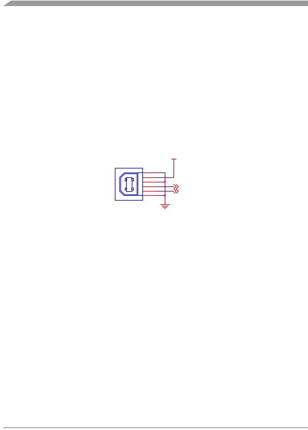
The USB connector is designated as J15. Figure 4-5 shows the connector pinout.
Figure 4-5. USB Connector Pinout
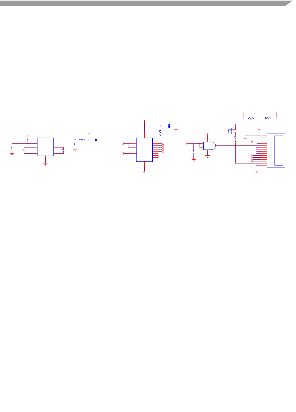
4.2.3.2 128x32 Graphic/Alphanumeric LCD
The 1323x-RCM supports a 128x32 pixel STN passive trans-reflective monochrome graphic LCD that
provides for alphanumeric or graphic readout. The LCD module is mounted on top of the main circuit
board and connects via a 16-pin connector. Figure 4-6 shows the LCD interface schematic.
• The display is an CRYSTALFONZ #CFAG12832A-YGH-N
• Viewing area is 51.0 (W) × 17.8 (H) mm
• The LCD operates from 5 Vdc generated from the main operating voltage through a boost
switching regulator. The LCD module requires a highly regulated 5 V so that the high voltages
generated onboard the display are consistent.
• The LCD has optional yellow-green LED backlighting
— Typical current of 30 mA when full on
— Enabled via Jumper J10
— Always on when enabled.
• LCD interface to the MCU is via the SPI port - although the LCD module only supports a parallel
interface (8-bit or 4-bit modes), the 1323x-RCM uses a serial interface derived from the SPI port
— The SPI serial stream is loaded into an 8-bit shift register (74AHCT164) used as a
serial-to-parallel converter
1
2
3
4
S1
S2
1
2
34
+D
-D
G
V
J15
USB_TY PE_B
DATA_P
DATA_M
V_BUS
1323x Remote Control Motherboard
1323x Development Hardware Reference Manual, Rev. 1.0
Freescale Semiconductor 4-11
— Nibble (4-bit) parallel mode is used on the LCD and the shift register provides the 4 data bits
and the RS control signal
— The 4-data and RS control are strobed into the LCD via the LCD_CTL0 control signal derived
from MC13233 PTA2 output.
— LCD write mode only is supported; the LCD cannot be read.
— The SPI port is shared with the serial FLASH on the 1323x-MRB. SS must be inactive (high)
when writing to the LCD
• The onboard controller is a member of the Sitronix ST7920 Series family with an integrated
display data RAM and alphanumeric character set
Figure 4-6. 1323x-RCM LCD Interface Circuit
4.2.3.3 36 Pushbutton 6x6 Switch Matrix
The1323x-RCM provides an 36 pushbutton 6x6 switch matrix for user application input interface.
• The matrix utilizes MC13233 KBI inputs
• All switches have interrupt and device wake up capability
• For these 36 switches
— Includes the pushbutton array
— Includes two switches located to the right and two switches to the left of the LCD
— Includes switches SW31 and SW32 located on the bottom (non-component) side of the board
— Does not support the two switches (KB0 and KB1) located near the touchpad.
4.2.3.4 Synaptics Touchpad
A Synaptics® Touchpad™ capacitive touch sensor is mounted on the 1323x-RCM for pointing
functionality.
• The touchpad is approximately 30mm tall x 45mm wide
• Interface to the MCU uses the IIC interface
• The touchpad has a separate interrupt request line that is tied to the KBI1P6 MCU input
• The MCU reset is tied to the touchpad and resets the touchpad whenever a system reset occurs
• The touchpad support two independent KBI signals that are connected to pushbuttons KB0 and
KB1and used for touchpad select functions
• The touchpad is soldered to the 1323x-RCM using two SMT headers
C31
0. 1 UF
R3 2
10K
R31
43
R30
1K
1 3
2
R5 3 5K
V_LC D
Q0
Q1
Q2
Q3
Q4
VSS
1
VDD
2
Vo
3
RS
4
R/W
5
E
6
DB0
7
DB1
8
DB2
9
DB3
10
DB4
11
DB5
12
DB6
13
DB7
14
ANODE
15
KATODE
16
DS1
LC D + HD R 1X16 + CON 1 X16
LC D_ CT L0
1
2
J10
HDR 1X2
8-B IT SH IFT REGI STER
3 5
4
2
1
U7
SN 74 A HC T1G08
Q0 3
Q1 4
Q2 5
Q3 6
Q4 10
Q5 11
Q6 12
Q7 13
VCC 14
GND
7
DSA
1
DSB
2
CP
8
MR 9
U6
74AHCT164
V_LC D
V_LCD
R51 3.3K
DN P
SPI_MOSI
SPI_CLK
VCC
V_LC D
C-
A1
C+
B1
V_IN
B3
EN
A3
GND
A2
V_OUT C1
C2+ C2
C2 - C3
U10
F AN 5665
C38
2. 2 uF
C44
2 . 2uF
R5 0
0
TP3 3
C45
2.2uF
C46
2. 2 uF
5 V BO OST CHARG E PU MP
LCD
VCC
V_5V
Q0
Q1
Q2
Q3
Q4
CON TRAST ADJ UST
V_LC D
V_LCD
1323x Remote Control Motherboard
1323x Development Hardware Reference Manual, Rev. 1.0
4-12 Freescale Semiconductor
Figure 4-7 shows the touchpad circuit.
Figure 4-7. 1323x-RCM Touchpad Circuit
4.2.3.5 3-Axis Accelerometer
The 1323x-RCM contains a Freescale MMA7660 3-axis accelerometer with IIC interface.
• Uses a 3mm x 3mm x 0.9mm DFN package
• Device interface supports IIC bus and system reset
• Supports an auto-wake/sleep feature for Low power consumption.
• When the device is in auto-sleep state, if a shake interrupt, tap interrupt, Delta G, or orientation
detection interrupt occurs, the device comes out of sleep mode and generates an interrupt request
via the IRQ signal
Figure 4-8 shows the accelerometer circuit.
Figure 4-8. 1323x-RCM Accelerometer Circuit
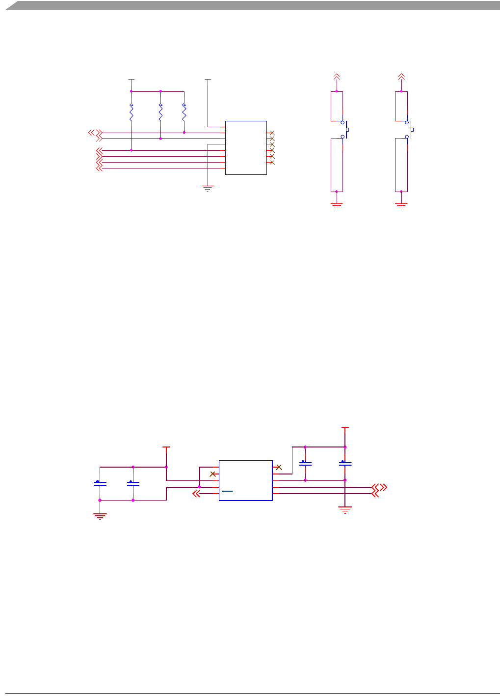
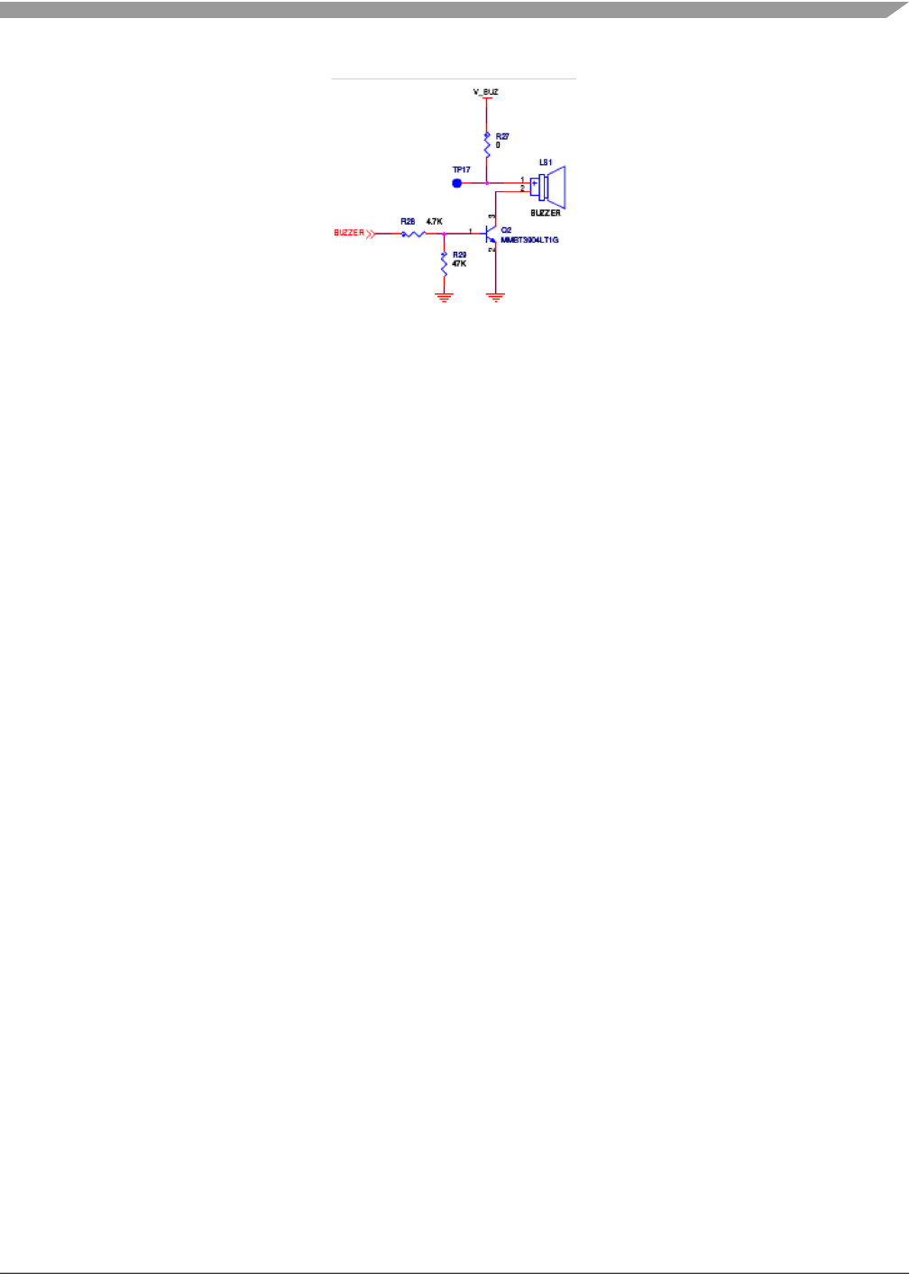
4.2.3.6 Buzzer
The 1323x-RCM provides a single tone audio buzzer.
• Device LS1, CUI Inc., Part No. CMI-1240
• 4.0 kHz resonant frequency
• Device is buffered by Q2 and active when MCU output PTA1 is high (see Table 4-3)
Figure 4-9 shows the buzzer circuit.
R52
10K
VDD
1
SDA
2
SCL
3
GND
4
IRQ
5
RESET
6
KBI 0
7
KBI 1
8
NC1 9
NC2 10
NC3 11
NC4 12
NC5 13
NC6 14
J11
TOUCHPAD
I2C_SDA
V_TPD
R34
10K
I2C_SCL
R33
10K
KBI1P6
TPKBI 1
TPKBI 0
RSTb
V_TPD
1
4
2
3
KB0
PB switch
TPKBI0 TPKBI1
1
4
2
3
KB1
PB switch
TPKBI 1TPKBI0
RESERVED
1
NC1
2
AVDD
3
AVSS
4
INT
5
NC2 10
DVDD 9
DVSS 8
SDA 7
SC L 6
U5
MMA7660FC
C28
10UF
C26
10UF
C29
0.1U F
C27
0.1UF
I2C_SDA
I2C_SCLIRQb
V_ACC
V_ACC
1323x Remote Control Motherboard
1323x Development Hardware Reference Manual, Rev. 1.0
Freescale Semiconductor 4-13
Figure 4-9. 1323x-RCM Buzzer Circuit
4.2.3.7 Blue Indicator LED
The1323x-RCM provides 4 blue LEDs for user application indicator outputs. Refer to Table 4-3 for
listings of the MC13233 outputs that drive the LEDs.
1323x Development Hardware Reference Manual, Rev. 1.0
4-14 Freescale Semiconductor
1323x Remote Control Motherboard
4.3 Schematic, Board Layout, and Bill of Material
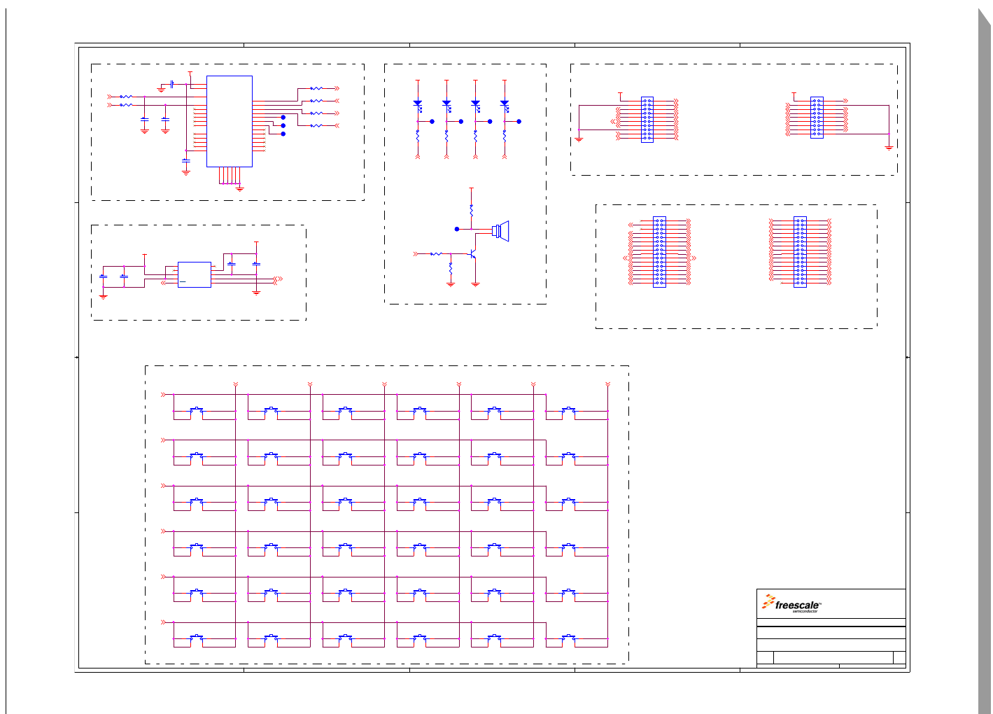
Figure 4-10. 1323x-RCM Schematic (1 of 3)
5
5
4
4
3
3
2
2
1
1
D D
C C
B B
A A
V_MRBV_MRB
V_LED V_LED V_LED V_LED
V_USB
V_ACC
V_ACC
V_BUZ
MRB-I2C_SDA
KBI1P0 KBI1P1 KBI1P2 KBI1P3 KBI1P4 KBI1P5
LED2 LED3 LED4LED1
MRB-RSTb
MRB-SPI_CLK
MRB-SPI_MISO
MRB-SPI_MOSI
MRB-SPI_SS
MRB-UART_RTS/KBI1P7
MRB-UART_CTS/TPM2
MRB-KBI1P0
MRB-KBI1P2
MRB-KBI1P1
MRB-KBI1P3
MRB-I2C_SCL
MRB-UART_TXD
MRB-UART_RXD
BUZZER
I2C_SCL
I2C_SDA
IRQb
MRB-TPM0
MRB-PTD7/32M_OUT
MRB-KBI1P5
MRB-KBI2P0
MRB-KBI2P2
MRB-PTA4/32K_OUT
MRB-PTA2/LCD_CTL0
MRB-KBI1P4
MRB-KBI1P6
MRB-KBI2P1
MRB-KBI2P3
MRB-PTA3/IRQb
MRB-PTD1/TPM1 MRB-PTD3/TPM3
MRB-PTD4/CMT
MRB-KBI1P3
MRB-KBI1P1
MRB-KBI1P2
MRB-KBI1P4
MRB-PTD4/CMT
MRB-SPI_MOSI
MRB-SPI_SS
MRB-KBI1P5
MRB-KBI1P0
MRB-KBI2P0
MRB-KBI2P2
MRB-PTD1/TPM1
MRB-PTD3/TPM3
SPI_MOSI
KMD0
KMD2
LED4
KBI1P3
KBI1P1
KBI1P2
KBI1P4
KMD4
KBI1P5
KBI1P0
DATA_P
DATA_M
UART_TXD
UART_RTS
UART_RXD
UART_CTS
MRB-KBI2P3
MRB-KBI2P1
MRB-KBI1P6
MRB-PTA4/32K_OUT
MRB-PTA3/IRQb
MRB-PTD7/32M_OUTKMD5
MRB-PTA2/LCD_CTL0LCD_CTL0
IRQb
KMD1
KBI1P6
KMD3
LED2
MRB-PTA1
MRB-PTA0
MRB-SPI_MISO
MRB-UART_TXDUART_TXD
MRB-SPI_CLKSPI_CLK
MRB-UART_RXDUART_RXD
MRB-RSTbRSTb
MRB-TPM0LED3
MRB-UART_RTS/KBI1P7UART_RTS
MRB-I2C_SDAI2C_SDA
MRB-UART_CTS/TPM2UART_CTS
MRB-I2C_SCLI2C_SCL
MRB-PTA0LED1
MRB-PTA1BUZZER
KMD0
KMD1
KMD2
KMD3
KMD4
KMD5
Drawing Title:
Size Document Number Rev
Date: Sheet of
Page Title:
ICAP Classification: FCP: FIUO: PUBI:
SCH-26116 PDF: SPF-26116 B1
1323X REMOTE CONTROL MOTHERBOARD
C
Friday, February 05, 2010
INTERFACE
35
X______
Drawing Title:
Size Document Number Rev
Date: Sheet of
Page Title:
ICAP Classification: FCP: FIUO: PUBI:
SCH-26116 PDF: SPF-26116 B1
1323X REMOTE CONTROL MOTHERBOARD
C
Friday, February 05, 2010
INTERFACE
35
X______
Drawing Title:
Size Document Number Rev
Date: Sheet of
Page Title:
ICAP Classification: FCP: FIUO: PUBI:
SCH-26116 PDF: SPF-26116 B1
1323X REMOTE CONTROL MOTHERBOARD
C
Friday, February 05, 2010
INTERFACE
35
X______
20-PIN GPIO
STANDARD HEADER
P1 & P2:
IO PIN MAPPING
MUST USE SHUNTS TO ENABLE
BOARD FUNCTIONALLITY.
GPIO
SOCKETS FOR 1323X-MRB ASSEMBLY
DIGITAL ACCELEROMETER
KEYBOARD MATRIX
USB/UART TRANSCEIVER
LED'S & BUZZER
GUIDE MP3 STOCK MENUPOWER
SK1 SK2 SK3 SK4
VOL+ VOL- CH+MUTE CH-
STOP PAUSE REC RW PLAY FF
TV
ENTERCLEAR9087
123456
R28 4.7KR28 4.7K
TP15TP15
C24
15PF
C24
15PF
SW18
PB switch
SW18
PB switch
1 4
2 3
SW8
PB switch
SW8
PB switch
1 4
2 3
SW32
PB switch
DNP
SW32
PB switch
DNP
1 4
2 3
SW26
PB switch
SW26
PB switch
1 4
2 3
LED4
BLUE
LED4
BLUE
21
LED1
BLUE
LED1
BLUE
21
LED3
BLUE
LED3
BLUE
21
LED2
BLUE
LED2
BLUE
21
C30
0.1UF
C30
0.1UF
TP14TP14
TP32TP32
TP31TP31
SW17
PB switch
SW17
PB switch
1 4
2 3
SW9
PB switch
SW9
PB switch
1 4
2 3
SK2
PB switch
SK2
PB switch
1 4
2 3
SW27
PB switch
SW27
PB switch
1 4
2 3
U5
MMA7660FC
U5
MMA7660FC
RESERVED
1
NC1
2
AVDD
3
AVSS
4
INT
5
NC2 10
DVDD 9
DVSS 8
SDA 7
SCL 6
SW10
PB switch
SW10
PB switch
1 4
2 3
SW25
PB switch
SW25
PB switch
1 4
2 3
SK4
PB switch
SK4
PB switch
1 4
2 3
SW1
PB switch
SW1
PB switch
1 4
2 3
R20 1KR20 1K
SW12
PB switch
SW12
PB switch
1 4
2 3
+
LS1
BUZZER
+
LS1
BUZZER
1
2
SW3
PB switch
SW3
PB switch
1 4
2 3
C28
10UF
C28
10UF
SW5
PB switch
SW5
PB switch
1 4
2 3
R23
390
R23
390
C25
0.1UF
C25
0.1UF
J9
CON_2X9
J9
CON_2X9
1 2
3 4
65
7 8
910
11 12
13 14
15 16
17 18
Q2
MMBT3904LT1G
Q2
MMBT3904LT1G
2 3
1
R22 1KR22 1K
SW28
PB switch
SW28
PB switch
1 4
2 3
SW24
PB switch
SW24
PB switch
1 4
2 3
R24
390
R24
390
R25
390
R25
390
C26
10UF
C26
10UF
R26
390
R26
390
R21 1KR21 1K
SW19
PB switch
SW19
PB switch
1 4
2 3
SW29
PB switch
SW29
PB switch
1 4
2 3
C29
0.1UF
C29
0.1UF
P1
HDR_2X16
P1
HDR_2X16
1 2
3 4
65
7 8
910
11 12
13 14
15 16
17 18
19 20
21 22
23 24
25 26
27 28
29 30
31 32
C23
15PF
C23
15PF
SW30
PB switch
DNP
SW30
PB switch
DNP
1 4
2 3
SW20
PB switch
SW20
PB switch
1 4
2 3
C27
0.1UF
C27
0.1UF
J8
CON_2X10
J8
CON_2X10
1 2
3 4
65
7 8
910
11 12
13 14
15 16
17 18
19 20
R48 0R48 0
R19 1KR19 1K
TP13TP13
R27
0
R27
0
TP30TP30
SW13
PB switch
SW13
PB switch
1 4
2 3
R49 0R49 0
SW21
PB switch
SW21
PB switch
1 4
2 3
TP17TP17
R29
47K
R29
47K
SW22
PB switch
SW22
PB switch
1 4
2 3
SW14
PB switch
SW14
PB switch
1 4
2 3
SW11
PB switch
SW11
PB switch
1 4
2 3
SK1
PB switch
SK1
PB switch
1 4
2 3
SW2
PB switch
SW2
PB switch
1 4
2 3
P2
HDR_2X16
P2
HDR_2X16
1 2
3 4
65
7 8
910
11 12
13 14
15 16
17 18
19 20
21 22
23 24
25 26
27 28
29 30
31 32
SW4
PB switch
SW4
PB switch
1 4
2 3
SW6
PB switch
SW6
PB switch
1 4
2 3
SW23
PB switch
SW23
PB switch
1 4
2 3
SW15
PB switch
SW15
PB switch
1 4
2 3
SW31
PB switch
DNP
SW31
PB switch
DNP
1 4
2 3
TP16TP16
U4 FT232RQU4 FT232RQ
GND1
4AGND
24
RI# 3
DCD# 7
DSR# 6
DTR# 31
3V3OUT
16
VCCIO
1
OSCI
27
RESET#
18
NC6
23
OSCO
28
CBUS4 9
CBUS3 11
CBUS1 21
CBUS0 22
CBUS2 10
NC5
29 NC4
25 NC3
13 NC2
12 NC1
5USBDP
14
USBDM
15
VCC
19
GND4
20 GND2
17
TEST
26
CTS# 8
RTS# 32
RXD 2
TXD 30
EP
33
SW16
PB switch
SW16
PB switch
1 4
2 3
SW7
PB switch
SW7
PB switch
1 4
2 3
SK3
PB switch
SK3
PB switch
1 4
2 3
1323x Remote Control Motherboard
1323x Development Hardware Reference Manual, Rev. 1.0
Freescale Semiconductor 4-15
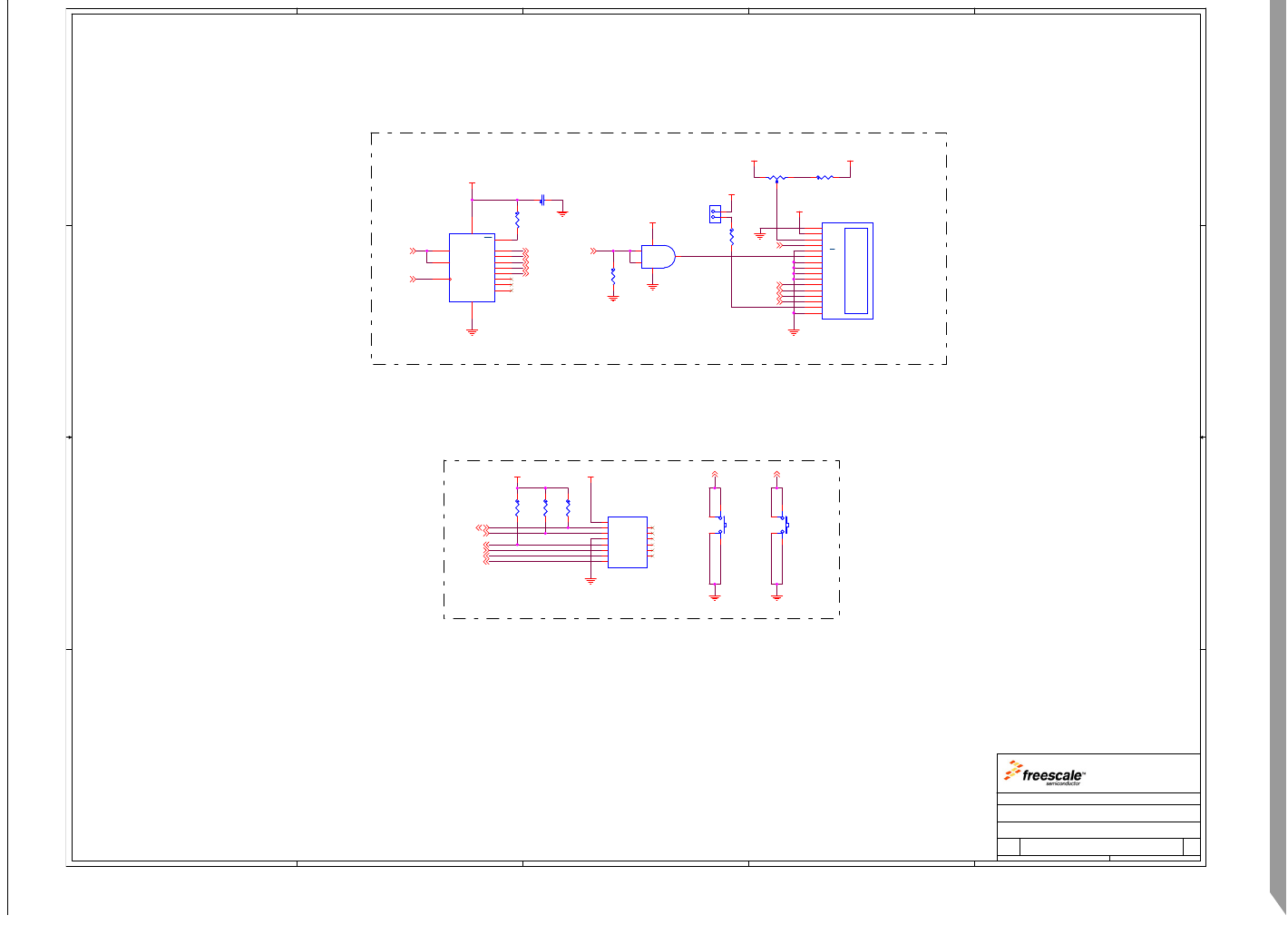
Figure 4-11. 1323x-RCM Schematic (2 of 3)
5
5
4
4
3
3
2
2
1
1
D D
C C
B B
A A
V_LCD
V_LCD
V_LCD
V_LCD
V_TPD V_TPD
V_LCD VCC
TPKBI0 TPKBI1
Q0
Q1
Q2
Q3
Q4
SPI_MOSI
SPI_CLK
Q0
Q1
Q2
Q3
Q4
LCD_CTL0
I2C_SDA
I2C_SCL
KBI1P6
RSTb
TPKBI0
TPKBI1
Drawing Title:
Size Document Number Rev
Date: Sheet of
Page Title:
ICAP Classification: FCP: FIUO: PUBI:
SCH-26116 PDF: SPF-26116 B1
1323X REMOTE CONTROL MOTHERBOARD
C
Friday, February 05, 2010
LCD & TOUCHPAD
45
X______
Drawing Title:
Size Document Number Rev
Date: Sheet of
Page Title:
ICAP Classification: FCP: FIUO: PUBI:
SCH-26116 PDF: SPF-26116 B1
1323X REMOTE CONTROL MOTHERBOARD
C
Friday, February 05, 2010
LCD & TOUCHPAD
45
X______
Drawing Title:
Size Document Number Rev
Date: Sheet of
Page Title:
ICAP Classification: FCP: FIUO: PUBI:
SCH-26116 PDF: SPF-26116 B1
1323X REMOTE CONTROL MOTHERBOARD
C
Friday, February 05, 2010
LCD & TOUCHPAD
45
X______
TPKBI1TPKBI0
LCD
TOUCHPAD
8-BIT SHIFT REGISTER
CONTRAST ADJUST
U6
74AHCT164
U6
74AHCT164
Q0 3
Q1 4
Q2 5
Q3 6
Q4 10
Q5 11
Q6 12
Q7 13
VCC 14
GND
7
DSA
1
DSB
2
CP
8
MR 9
R34
10K
R34
10K
R53 5K
R53 5K
1 3
2
KB1
PB switch
KB1
PB switch
1
4
2
3
U7
SN74AHCT1G08
U7
SN74AHCT1G08
3 5
4
2
1
R33
10K
R33
10K
C31
0.1UF
C31
0.1UF
R32
10K
R32
10K
R30
1K
R30
1K
R31
43
R31
43
J11
TOUCHPAD
J11
TOUCHPAD
VDD
1
SDA
2
SCL
3
GND
4
IRQ
5
RESET
6
KBI0
7
KBI1
8
NC1 9
NC2 10
NC3 11
NC4 12
NC5 13
NC6 14
R51 3.3K
DNP
R51 3.3K
DNP
R52
10K
R52
10K
J10
HDR 1X2
J10
HDR 1X2
1
2
DS1
LCD + HDR 1X16 + CON 1X16
DS1
LCD + HDR 1X16 + CON 1X16
VSS
1
VDD
2
Vo
3
RS
4
R/W
5
E
6
DB0
7
DB1
8
DB2
9
DB3
10
DB4
11
DB5
12
DB6
13
DB7
14
ANODE
15
KATODE
16
KB0
PB switch
KB0
PB switch
1
4
2
3
1323x Remote Control Motherboard
1323x Development Hardware Reference Manual, Rev. 1.0
Freescale Semiconductor 4-16
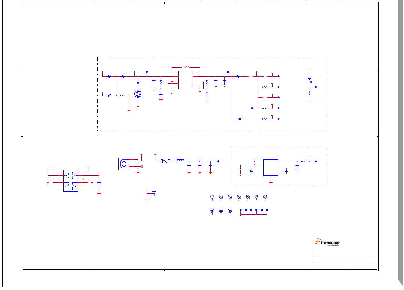
Figure 4-12. 1323x-RCM Schematic (3 of 3)
5
5
4
4
3
3
2
2
1
1
D D
C C
B B
A A
V_5V
V_3V3
V_LED
V_LED
V_TPD
V_ACC
VCC
V_USB
V_BUS V_SER
V_BAT
V_MRB
V_LCD
V_MAIN
VCC
V_JACK
V_DC
V_USB
V_BHL
V_SER
V_BUS
V_BAT
V_BUZ
V_DC
V_JACK
V_SER
V_BUS
DATA_M
DATA_P
Drawing Title:
Size Document Number Rev
Date: Sheet of
Page Title:
ICAP Classification: FCP: FIUO: PUBI:
SCH-26116 PDF: SPF-26116 B1
1323X REMOTE CONTROL MOTHERBOARD
C
Friday, February 05, 2010
POWER MANAGEMENT
55
X ______
Drawing Title:
Size Document Number Rev
Date: Sheet of
Page Title:
ICAP Classification: FCP: FIUO: PUBI:
SCH-26116 PDF: SPF-26116 B1
1323X REMOTE CONTROL MOTHERBOARD
C
Friday, February 05, 2010
POWER MANAGEMENT
55
X ______
Drawing Title:
Size Document Number Rev
Date: Sheet of
Page Title:
ICAP Classification: FCP: FIUO: PUBI:
SCH-26116 PDF: SPF-26116 B1
1323X REMOTE CONTROL MOTHERBOARD
C
Friday, February 05, 2010
POWER MANAGEMENT
55
X ______
LED
TOUCHPAD
ACCELEROMETER
POWER ON
3.3V BUCK/BOOST REGULATOR
TO USE TPS63000,
REPLACE RESISTORS WITH
THE FOLLOWING VALUES:
R45 = 100 OHM, R47 = 1.24M
AND POPULATE R46.
OUTPUT VOLTAGE WILL BE 3.6V
MODULAR REFERENCE BOARD
5V BOOST CHARGE PUMP
LCD
3.3V POWER NETWORK
5V POWER NETWORK
EXTERNAL SUPPLY.
NEVER SHUNT!!!
BUZZER
F1
0.5A
F1
0.5A
1 2
TP22TP22
BH2
125
BH2
125
R39
330
R39
330
L3 3.3uHL3 3.3uH
1 2
TL4TL4
C33
0.1UF
C33
0.1UF
BT1
BATTERY HOLDER
BT1
BATTERY HOLDER
12
D8
MBR0520LT1G
D8
MBR0520LT1G
R37
0
R37
0
C32
10UF
C32
10UF
R46
200K
DNP
R46
200K
DNP
FID1
FID
FID1
FID
R35
0
R35
0
BH6
125
BH6
125
TL1TL1
D11
MBR0520LT1G
D11
MBR0520LT1G
C42
10UF
C42
10UF
D9
MBR0520LT1G
D9
MBR0520LT1G
TL5TL5
U9
FAN5665
U9
FAN5665
C-
A1
C+
B1
V_IN
B3
EN
A3
GND
A2
V_OUT C1
C2+ C2
C2- C3
LED5
RED
LED5
RED
21
BH3
125
BH3
125
R42
0
R42
0
TP24TP24
D12
MBR0520LT1G
D12
MBR0520LT1G
C34
2.2uF
C34
2.2uF
R41
10K
R41
10K
C39
0.1UF
C39
0.1UF
SL1
4P2T SWITCH
SL1
4P2T SWITCH
1
2
3
4
5
6 7
8
9
10
11
12
C37
2.2uF
C37
2.2uF
1
2
34
+D
-D
G
V
J15
USB_TYPE_B
1
2
34
+D
-D
G
V
J15
USB_TYPE_B
1
2
3
4
S1
S2
C43
10UF
C43
10UF
TP26TP26
R38
4.7K
R38
4.7K
R45
0
R45
0
FID2
FID
FID2
FID
L4
60OHM
L4
60OHM
1 2
TL2TL2
TP28TP28
U8
TPS63001
U8
TPS63001
EN
6
GND
9
L1
4L2 2
PS/SYNC
7
VOUT 1
VIN
5
VINA
8
FB 10
PGND 3
PPAD 11
TP25TP25
BH4
125
BH4
125
R43
0
R43
0
R40
0
R40
0
TP29TP29
D10
MBR0520LT1G
D10
MBR0520LT1G
R47
0
R47
0
TP27TP27
TP19TP19
R36
0
R36
0
BH7
125
BH7
125
TP23TP23
D13
MBR0520LT1G
D13
MBR0520LT1G
BH1
125
BH1
125
TP21TP21
TP20TP20
C40
4.7uF
C40
4.7uF
FID3
FID
FID3
FID
TL3TL3
R44
0
R44
0
C41
0.01UF
C41
0.01UF
C35
2.2uF
C35
2.2uF
BH5
125
BH5
125
J14
HDR 1X2
J14
HDR 1X2
1
2
C36
2.2uF
C36
2.2uF
TL6TL6
Q3
SI2305
Q3
SI2305
1
32
1323x Remote Control Motherboard
1323x Development Hardware Reference Manual, Rev. 1.0
Freescale Semiconductor 4-17
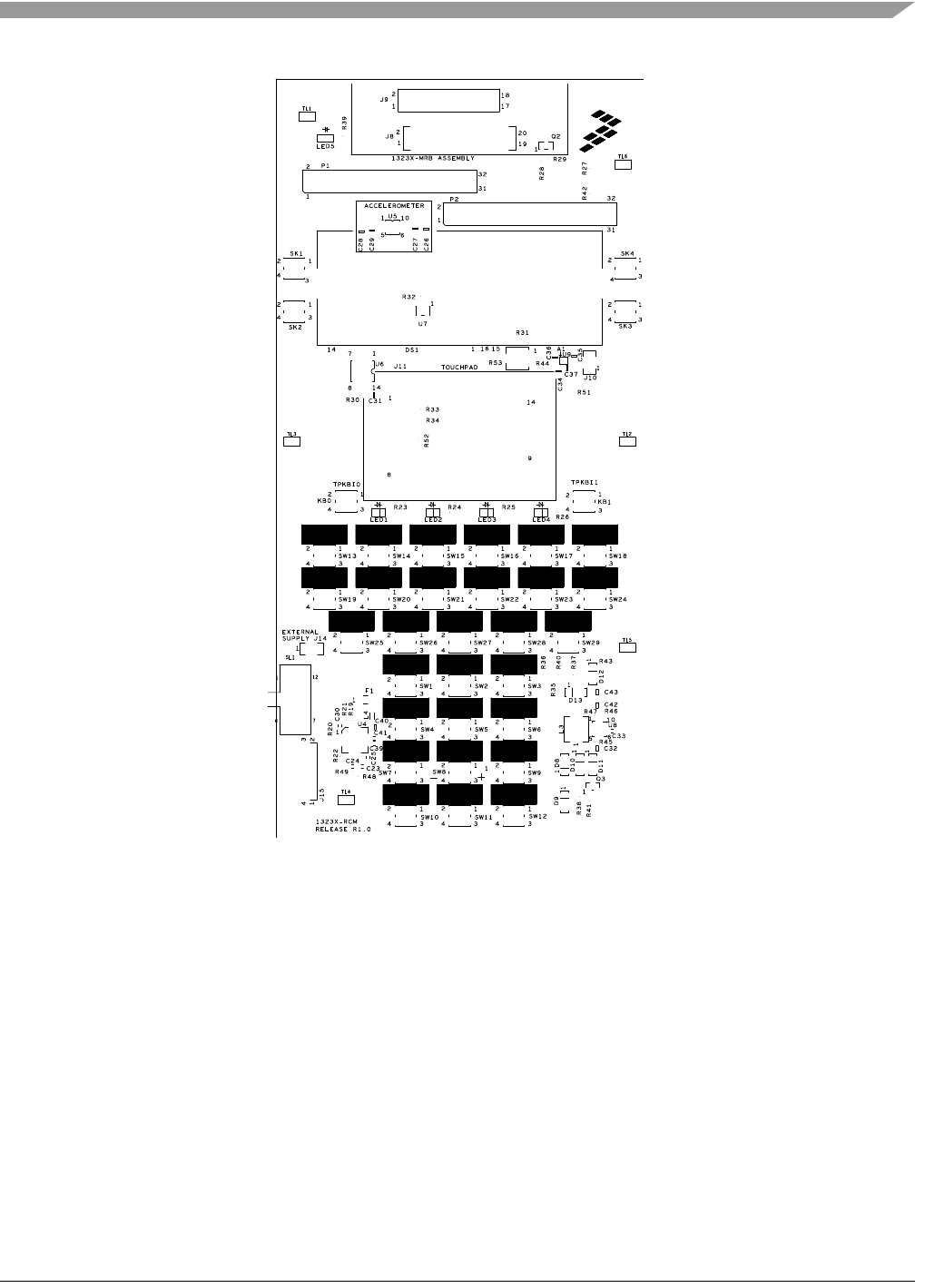
Figure 4-13. 1323x-RCM PCB Component Location (Top View)
1323x Remote Control Motherboard
1323x Development Hardware Reference Manual, Rev. 1.0
4-18 Freescale Semiconductor
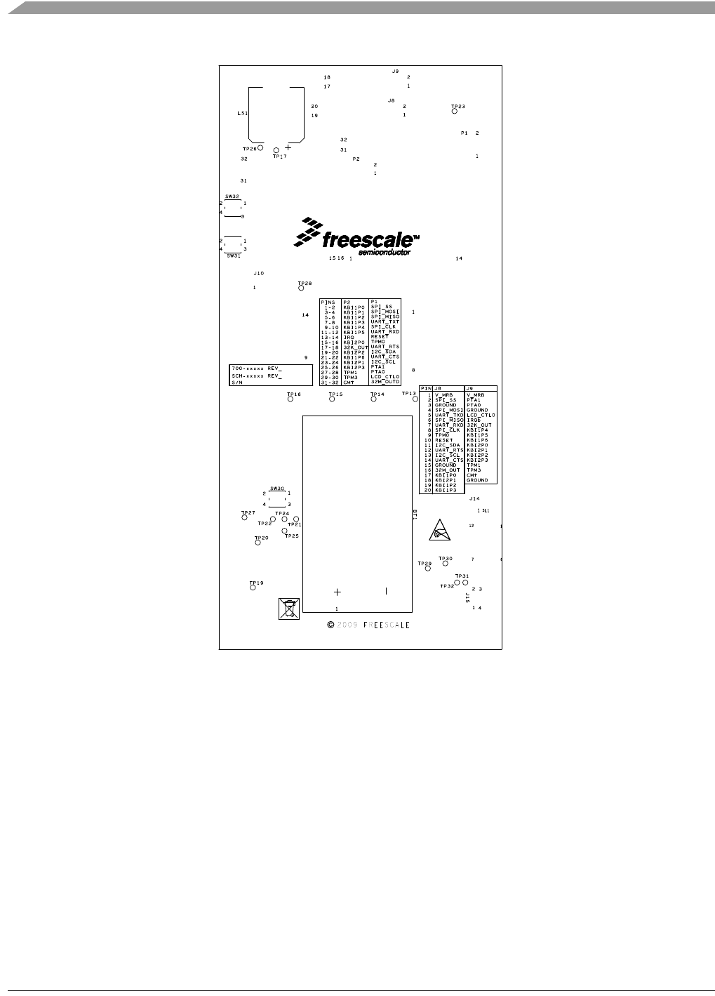
Figure 4-14. 1323x-RCM PCB Test Points
1323x Remote Control Motherboard
1323x Development Hardware Reference Manual, Rev. 1.0
Freescale Semiconductor 4-19
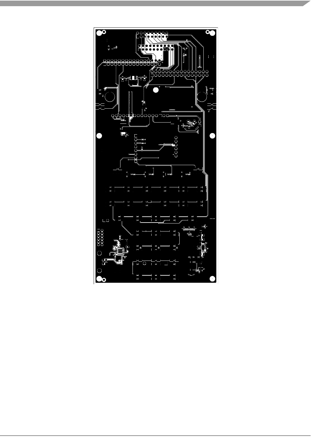
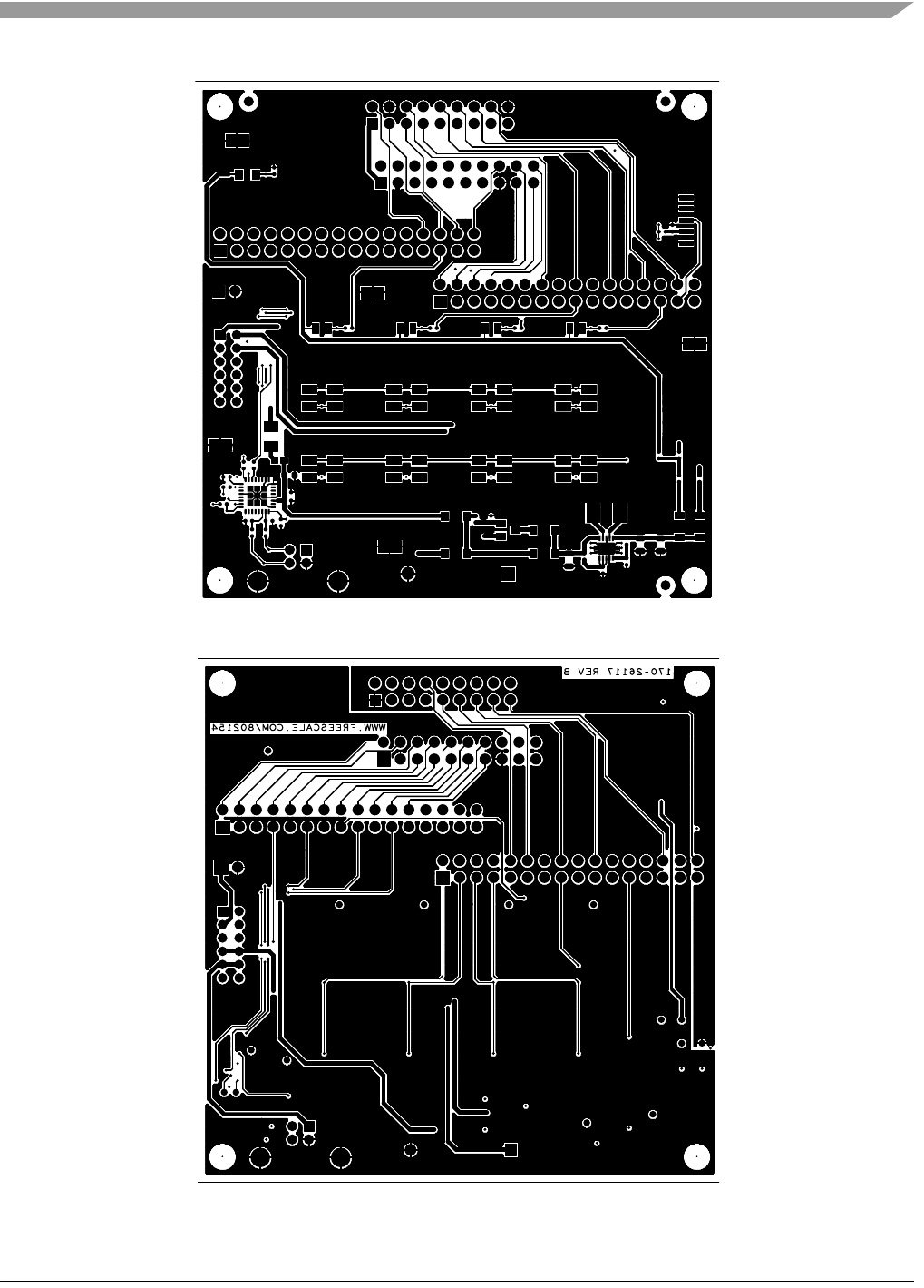
Figure 4-15. 1323x-RCM PCB Layout (Top View)
1323x Remote Control Motherboard
1323x Development Hardware Reference Manual, Rev. 1.0
4-20 Freescale Semiconductor
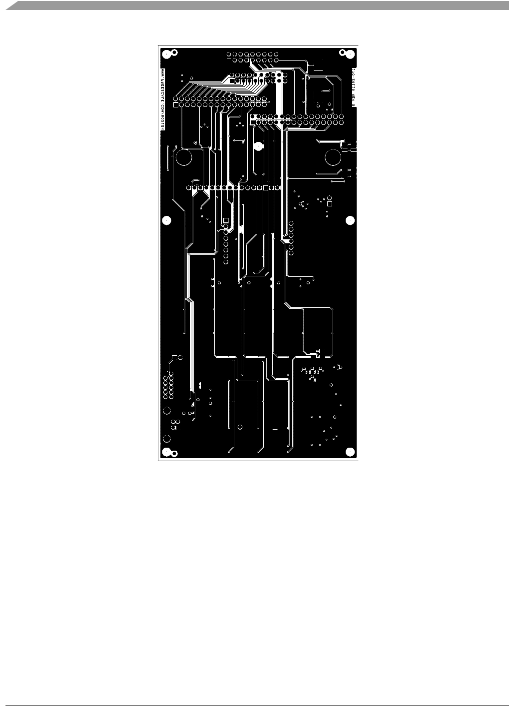
Figure 4-16. 1323x-RCM PCB Layout (Bottom View)
1323x Remote Control Motherboard
1323x Development Hardware Reference Manual, Rev. 1.0
Freescale Semiconductor 4-21
4.3.1 1323x-RCM Bill of Materials
Table 4-4. Bill of Materials
Item Qty. Reference Value Description Mfg. Name Mfg. Part Number
1 8 BH1,BH2,BH3,BH
4,BH5,BH6,BH7,B
H8
125 NON-PLATED MOUNTING
HOLE 125 DRILL / 160
KEEPOUT NO PART TO
ORDER
21BT1 BATTERY
HOLDER
BATTERY HOLDER 2XAA TH Keystone
Electronics
2462
3 2 C23,C24 15PF CAP CER 15PF 50V 5% C0G
0402
Kemet C0402C150J5GAC
4 4 C25,C30,C33,C39 0.1UF CAP CER 0.1UF 16V 10% X7R
0402
Murata GRM155R71C104KA88D
5 5 C26,C28,C32,C42
,C43
10UF CAP CER 10UF 10V 10% X7R
0805
Murata GRM21BR71A106KE51L
6 3 C27,C29,C31 0.1UF CAP CER 0.1UF 50V 10% X7R
0603
Murata GRM188R71H104KA93D
7 4 C34,C35,C36,C37 2.2uF CAP CER 2.2UF 6.3V 10% X5R
0603
Murata GRM188R60J225KE19D
8 1 C40 4.7uF CAP CER 4.7UF 10V 10% X5R
0603
Taiyo Yuden LMK107BJ475KA-T
9 1 C41 0.01UF CAP CER 0.01UF 10V 20%
X7R 0402
Avx 0402ZC103MAT2A
10 1 DS1 LCD + HDR
1X16 + CON
1X16
SUBASSY LCD 128X32 DOT
4.5-5V TH + HDR 1X16 TH
100MIL SP 330H AU + CON
1X16 SKT TH 100MIL SP 335
AU
Freescale
Semiconductor
370-76474, 210-75955,
210-77812
11 6 D8,D9,D10,D11,D
12,D13
MBR0520LT
1G
DIODE SCH 0.5A 20V
SOD-123
On
Semiconductor
MBR0520LT1G
12 3 FID1,FID2,FID3 FID FIDUCIAL 060 MIL PAD W/120
SOLDERMASK AND 040 MIL
PAD W/90 MIL SOLDERMASK
NO PART TO ORDER
Generic FID-040
13 1 F1 0.5A FUSE FAST 0.5A 63V SMT
1206
Littelfuse 0437.500WR
14 1 J8 CON_2X10 CON 2X10 SKT TH 100MIL
CTR 335H AU 104L
Samtec SSW-110-01-G-D
15 1 J9 CON_2X9 CON 2X9 SKT TH 100MIL SP
335H AU 194L
Samtec SSW-109-02-G-D
16 2 J10,J14 HDR_1X2 HDR 1X2 TH 100MIL SP 375H
AU
Tyco
Electronics
826629-2
17 1 J11 TOUCHPAD TOUCHPAD SERIAL 3V TH Synaptics, Inc 515-000188-0110

1323x Remote Control Motherboard
1323x Development Hardware Reference Manual, Rev. 1.0
4-22 Freescale Semiconductor
18 1 J15 USB_TYPE_
B
CON 2X2 USB_TYPE_B SKT
RA SHLD TH 2.5MM SP 453H
AU
Tyco
Electronics
292304-2
19 35 SW1,SK1,KB1,SW
2,SK2,SW3,SK3,S
W4,SK4,SW5,SW
6,SW7,SW8,SW9,
SW10,SW11,SW1
2,SW13,SW14,S
W15,SW16,SW17,
SW18,SW19,SW2
0,SW21,SW22,S
W23,SW24,SW25,
SW26,SW27,SW2
8,SW29,KB0
PB switch SW SMT 4.0MM FMS 0.1A
MAX 16V MAX ROHS
COMPLIANT
Bourns 7914J-1-000E
20 4 LED1,LED2,LED3,
LED4
BLUE LED BLUE SGL 20MA SMT
0805
Lite On LTST-C171TBKT-5A
21 1 LED5 RED LED RED CLEAR SGL 30MA
SMT 0805
Lite On LTST-C171KRKT
22 1 LS1 BUZZER BUZZER PIEZO AUDIO 83DB
4KHZ 8MA 12V SMT
Cui Stack CMI-1240
23 1 L3 3.3uH IND PWR 3.3UH@100KHZ
3.3A 20% SMT
Vishay
Intertechnology
IHLP2020BZER3R3M01
24 1 L4 60OHM IND FER BEAD
60OHM@100MHZ 500MA --
0603
Murata BLM18PG600SN1_
25 2 P1,P2 HDR_2X16 HDR 2X16 TH 100MIL CTR
330H AU 100L
Samtec TSW-116-07-S-D
26 1 Q2 MMBT3904L
T1G
TRAN NPN GEN 200MA 40V
SOT-23
On
Semiconductor
MMBT3904LT1G
27 1 Q3 SI2305 TRAN PMOS PWR 4.1A 8V
SOT23
Vishay
Intertechnology
SI2305ADS-T1-GE3
28 5 R19,R20,R21,R22
,R30
1K RES MF 1.0K 1/16W 5% 0402 Vishay
Intertechnology
CRCW04021K00JNED
29 4 R23,R24,R25,R26 390 RES MF 390 OHM 1/16W 5%
0402
Bourns CR0402-JW-391GLF
30 2 R27,R45 100 RES MF 100 OHM 1/16W 5%
0402
Vishay
Intertechnology
CRCW0402100RJNED
31 10 R28,R35,R36,R37
,R40,R42,R43,R4
4,R48,R49
0 RES TF ZERO OHM 1/16W
RC0402
Vishay
Intertechnology
CRCW04020000ZS
32 6 R29,R32,R33,R34
,R41,R52
10K RES MF 10K 1/16W 5% 0402 Vishay
Intertechnology
CRCW040210K0JNED
Table 4-4. Bill of Materials
Item Qty. Reference Value Description Mfg. Name Mfg. Part Number
1323x Remote Control Motherboard
1323x Development Hardware Reference Manual, Rev. 1.0
Freescale Semiconductor 4-23
33 1 R31 39 RES MF 39 OHM 1/16W 5%
0402
Smec RC73L2Z390JTF
34 1 R38 4.7K RES MF 4.7K 1/16W 5% 0402 Smec RC73L2Z472JTF
35 1 R39 330 RES MF 330 OHM 1/16W 5%
0402
Vishay
Intertechnology
CRCW0402330RJNED
36 1 R46 200K RES MF 200K 1/16W 5% 0402 Yageo America RC0402JR-07200KL
37 1 R47 1.24M RES MF 1.24M 1/16W 1%
0402
Vishay
Intertechnology
CRCW04021M24FKED
38 1 R50 5K RES POT 5.0K 1/4W 20% SMT Bourns 3314J-1-502E
39 1 R51 3.3K RES MF 3.3K 1/16W 5% 0402 Vishay
Intertechnology
CRCW04023K30JNED
40 1 SL1 4PDT
SWITCH
SW 4PDT SLD TH RA 30V
100MA --
Tyco
Electronics
1-1437575-1
41 3 SW30,SW31,SW3
2
PB switch SW SMT 4.0MM FMS 0.1A
MAX 16V MAX ROHS
COMPLIANT
Bourns 7914J-1-000E
42 19 TP13,TP14,TP15,
TP16,TP17,TP19,
TP20,TP21,TP22,
TP23,TP24,TP25,
TP26,TP27,TP28,
TP29,TP30,TP31,
TP32
TPAD_040 TEST POINT PAD 40MIL DIA
SMT, NO PART TO ORDER
Notacomponent NOTACOMPONENT
43 1 U4 FT232RQ IC XCVR USB TO UART CTLR
3.3-5.25V QFN32
Future
Technology
Devices
International
Ltd.
FT232RQ
44 1 U5 MMA7660F
C
IC SENSOR
ACCELEROMETER 2.4-3.6V
DFN10
Freescale
Semiconductor
MMA7660FC
45 1 U6 74AHCT164 IC REG SHIFT SER/PAR 8BIT
4.5-5.5V TSSOP14
Nxp
Semiconductors
74AHCT164PW,112
46 1 U7 SN74AHC
T1G08
IC GATE AND SGL
2-INPUT POSITIVE
4.5-5.5V SOT23-5
Texas Instru-
ments
SN74AHCT1G08DBVR
47 1 U8 TPS63001 IC LIN DCDC SYNC 3.3V
OUTPUT 1250-1800KHZ
1.8-5.5V QFN-10
Texas Instru-
ments
TPS63001DRCT
Table 4-4. Bill of Materials
Item Qty. Reference Value Description Mfg. Name Mfg. Part Number

1323x Remote Control Motherboard
1323x Development Hardware Reference Manual, Rev. 1.0
4-24 Freescale Semiconductor
48 1 U9 FAN5665 IC LIN DCDC SWT 5V
2.9-5.5V WLCSP-8
Fairchild FAN5665UCX
Table 4-4. Bill of Materials
Item Qty. Reference Value Description Mfg. Name Mfg. Part Number

1323x Development Hardware Reference Manual, Rev. 1.0
Freescale Semiconductor 5-1
Chapter 5
1323x Remote Extender Motherboard
5.1 1323x-REM Overview
The 1323x-Remote Extender Motherboard (1323x-REM) is a motherboard that accepts the
1323x-Modular Reference Board (1323x-MRB) plug-in module (daughtercard) and supplies a power
supply and set of interface peripherals. The two boards in combination provide a simple platform to
evaluate the MC1323x, develop software, and demonstrate IEEE 802.15.4 based networking capabilities.
5.1.1 Features
The 1323x-REM provides the following features:
• Small form factor (3.1 x 3.1 inches)
• 2-Layer metal, 0.034 inch thick FR4 board
• Two connectors provide daughter card mounting
— 20-Pin primary connector
— 18-Pin secondary connector
— Provide main supply voltage to board
— Provide access to all MC13233 GPIO
• Flexible power supply
— Sources include USB port, two AA batteries, or DC source
— Power-On LED
—On-Off switch
• USB <> UART serial port
• 2x4 Switch matrix
• IR receiver
• Four application controlled blue indicator LEDs
• Secondary set of pin headers uses jumpers to enable/disable IO connections and allows user
application connection to MC13233 GPIO
1323x Remote Extender Motherboard
1323x Development Hardware Reference Manual, Rev. 1.0
5-2 Freescale Semiconductor
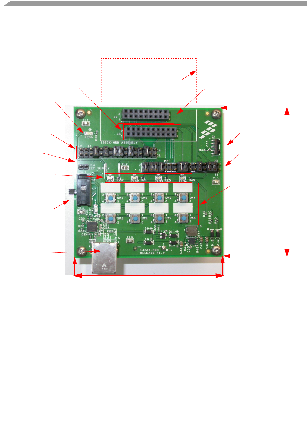
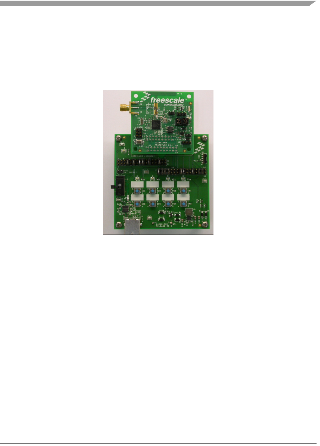
5.1.2 Form Factor
Figure 5-1 shows a photo of the 1323x-REM showing the locations of connectors and headers.
Figure 5-1. 1323x-REM
The1323x-MRB mounts on the 1323x-REM via receptacles J8 and J9. Figure 5-1 shows an outline of the
1323x-MRB placement when mounted.
2x4 Switch
USB
Primary 20-Pin IO
Connector (J8)
On / Off
Secondary 18-Pin IO
Connector (J9)
IR Receiver
Matrix
Connector J15
Switch
SL1
1323x-MRB Outline
(When mounted)
4 Blue LEDs
External
Supply
J14
Power-On
LED
GPIO Enable
Pin Header
P1
GPIO Enable
Pin Header
P2
3.1 Inches
79 mm
3.1 Inches
79 mm
1323x Remote Extender Motherboard
1323x Development Hardware Reference Manual, Rev. 1.0
Freescale Semiconductor 5-3
5.1.3 Board Level Specifications
NOTE
Temperature range specifications apply to REM used in combination with
MRB.
Table 5-1. 1323x-REM Specifications
Parameter Units Notes/Conditions
MIN TYP MAX
General
Size (PCB: X, Y) 79 x 79
3.1 x 3.1
mm
inches
Layer build (PCB) 0.8
0.034
mm
inches
2-Layer
Dielectric material (PCB) FR4
Power
Voltage supply (DC) 2.3 5 6 V
Voltage supply (USB) 4.4 5 5.25 V USB 2.0/1.1 standard specification
Voltage supply (Batteries) 2.8 3.2 V
Current consumption 100 mA
Temperature
Operating temperature; non-battery
operation (see note)
-20 +25 +70 °C Operating temperature is limited to +70 °C
due to switches. Basic circuit is good for a
maximum temperature of +85 °C.
Operating temperature; battery
operation (see note)
0 +25 +50 °C Operating temperature is limited by battery
temperature range
Storage temperature -30 +25 +70 °C
USB interface USB 2.0 and 1.1 full-speed compatible
IR Receiver
Carrier frequency 38 kHz
Angle of half transmission distance +/-50 degrees
Regulatory Approval
CE (ETSI) Product is approved accordingly to the EN
300 328 V1.7.1 (2006-10) standard
CE (EMC) Product is approved accordingly to the EN
301 489-1 V1.6.1 (2005-09) and EN 301
489-17 V1.2.1 (2002-08) standards
Safety

1323x Remote Extender Motherboard
1323x Development Hardware Reference Manual, Rev. 1.0
5-4 Freescale Semiconductor
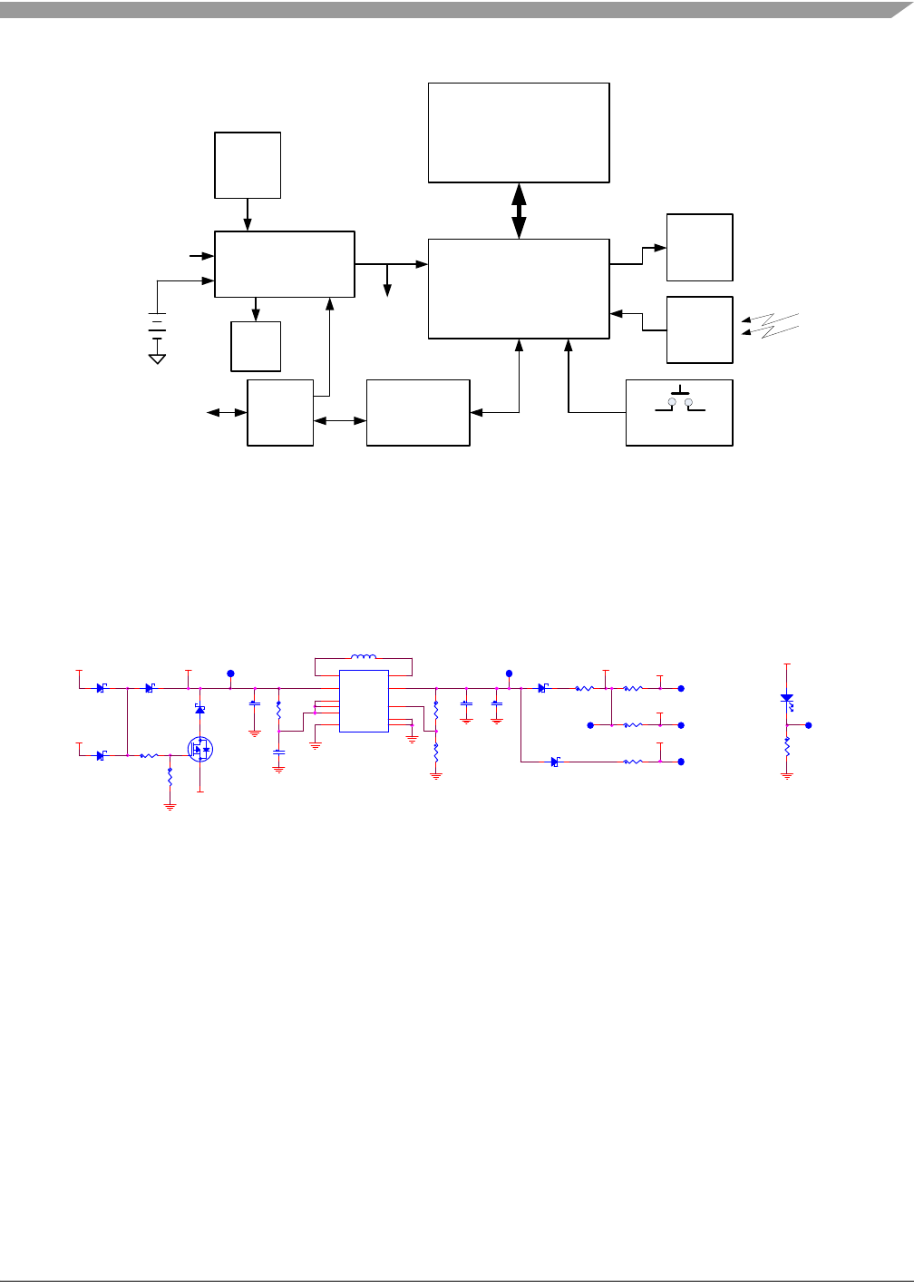
5.2 Functional Description
The 1323x-REM is a simple host motherboard for the 1323x-MRB. The two-board combination provides
a simple evaluation and development platform for the MC13233. Figure 5-2 shows a simple block
diagram. The 2-layer board provides a flexible power supply, eight pushbutton matrix, four indicator
LEDs, IR receiver, and a USB <> UART serial port.
As the board name implies this platform is useful to develop the host side (such as a DTV or entertainment
console) of an RF remote control application. The MC13233 provides the RF node and an IR receiver is
available to support legacy IR protocol remotes. Connection to a host is available through the USB port or
any of the other generic MC13233 communications ports.
The 1323x-REM is also recommended for target development of applications where there is little
periphery circuitry. There are switches and indicator LEDs onboard for user interface, and if necessary,
custom circuitry can be connected via the two pin headers that allow access to the MC13233 GPIO.
In the following sections, refer to:
•Figure 5-1 for location of connectors and features
•Figure 5-2 for the functional blocks
•Figure 5-8 and Figure 5-9 for the board schematic
UL Product is approved accordingly to the IEC
60950-1 and EN 60950-1, First Edition
standards
Environment
RoHS Product complies with the EU Directive
2002/95/EC of 27 January 2003
WEEE Product complies with the EU Directive
2002/95/EC of 27 January 2003
Table 5-1. 1323x-REM Specifications (continued)
Parameter Units Notes/Conditions
1323x Remote Extender Motherboard
1323x Development Hardware Reference Manual, Rev. 1.0
Freescale Semiconductor 5-5
Figure 5-2. 1323x-REM Block Diagram
5.2.1 Power Management
The 1323x-REM can be powered from two AA batteries, the USB connector 5 V supply, or an external
DC supply and is also intended to power the 1323x-MRB. Figure 5-3 shows the power management
circuit.
Figure 5-3. 1323x-REM Power Management Circuit
A boost-buck voltage regulator U8 is used in this design to allow operation over a relatively wide, low
voltage input range, i.e., the TPS63001 regulator has input voltage range from 1.8 V to 5.5V. This allows
a broad range of power supply sources. The regulated output voltage of the TPS63001 is 3.3 V which
delivers about 3.05 V to the board due to the drop across the isolation Schottky diodes.
Attributes of the power management circuit include:
• Switch SL1 provides an ON/OFF function for all input voltage sources
• Red LED5 provides a POWER-ON indicator for all sources
• The 1323x-REM can derive power from three different sources -
1. USB port Type-B connector J15 - power can be supplied from an actual USB port connection
or from an AC to DC converter that uses the USB connector to supply power.
2. External DC source via header J14 - a standard 0.1 in. spacing 1x2 pin header allows for
connection of an external DC supply.
1323x-MRB
GPIO Header
Receptacles
IR
Receiver
(38 kHz)
VCC
USB
2.0
4 Blue
Indicator
LEDs
USB
Type-B
Conn
On/Off
Switch
USB <> UART
Serial IC 8 Switch
Matrix
Power
Management GPIO
Pin Headers
On
LED
External DC
2 AA
Battery
IR
D8
MBR 0 52 0L T1 G
D10
MBR0520LT1G
D11
MBR 05 20 LT1 G
D12
MBR0520LT1G
D13
MBR0520LT1G
21
LED 5
RE D
POWER ON
R39
330
V_LED
V_ MRB
V_ LE D
V_DC
V_I RX
C32
10UF EN
6
GN D
9
L1
4L2 2
PS/SY N C
7
VOUT 1
VIN
5
VINA
8
FB 10
PGND 3
PPAD 11
U8
T PS6 30 01
1 2
L3 3.3uH
V_BAT
R38
4. 7 K
1
32
Q4
S I 23 05
R41
10K
TP27
V_USB VCC
TP21
TP 25 TP24
C33
0.1UF
R45
0
C43
10UF
R43
0
TP2 3
C42
10 U F
R35
0
R36
0
R40
0
INFRARRED RX
LED
V_MA IN
R46
200K
DNP
MODULAR REFERENCE BOARD
R47
0
V_ 3V6
TP1 9 TP20
D9
MBR 0 52 0L T1 G

1323x Remote Extender Motherboard
1323x Development Hardware Reference Manual, Rev. 1.0
5-6 Freescale Semiconductor
3. Battery Operation - a battery holder that accommodates two AA batteries is mounted on the
non-component (back) side of the board and provides for battery operation.
– If either the USB or external DC source is present, the battery source is disabled by
MOSFET transistor Q3
– The sources are all isolated and protected by Schottky diodes
– The minimum effective battery operating voltage is controlled by the use the FTDI
FT232RQ USB <> UART device - leakage current back through the FT232RQ UART
connections to the MC13233 on the MRB can cause the Q3 MOSFET to partially turnoff at
battery voltage below approximately 2.7-2.8 Vdc.
NOTE
To avoid current leakage through the USB device and lower minimum
battery operating voltage for battery-only operation, remove the following
jumpers:
• P1, Pins 7-8
• P1, Pins 11-12
• P1, Pins 17-18
• P1, Pins 21-22
NOTE
When battery operation is used, the temperature range of the two board
system should be limited to within the specified temperature range of the
battery technology. Table 5-1 limits temperature range from 0 °C to +50 °C
when battery operation is applied.
Table 5-2 lists the voltage source attributes.
Table 5-2. 1323x-REM Voltage Sources
Source Connector Input Voltage
Range Description
USB Port USB Type-B J15 4.4 V - 5.25 V • The input voltage range is set to the USB specification value
• The voltage can be supplied by either a standard USB cable
connection or an AC to DC power adaptor that uses the USB
connector J15
• If a power adaptor is in use, the USB serial port cannot be
used
External DC Supply 1x2 Pin Hdr J14 2.3 V - 6 V The input voltage range is determined by the U8 regulator and
the diode isolation circuit
Two AA Batteries Battery Holder 2.0 V - 3.1 V1
1The minimum operating battery voltage is determined by use model, see Note, Section 5.2.1, “Power Management”
• The input voltage range reflects the usable range of alkaline
cells and the voltage drop incurred by the diode isolation
circuit.
• The battery source is disabled if another source is connected
1323x Remote Extender Motherboard
1323x Development Hardware Reference Manual, Rev. 1.0
Freescale Semiconductor 5-7
Again referring to Figure 5-3, a number of zero-ohm resistors are provided to isolate different circuits and
to allow current measurement:
• VCC (main 1323x-REM supply) - resistor R35
• V_LED (all LEDs supply) - resistor R36
• V_IRX (IR receiver supply) - resistor R40
• V_MRB (1323x-MRB supply) - resistor R43
Figure 5-4. 1323x-MRB Mounted on 1323x-REM
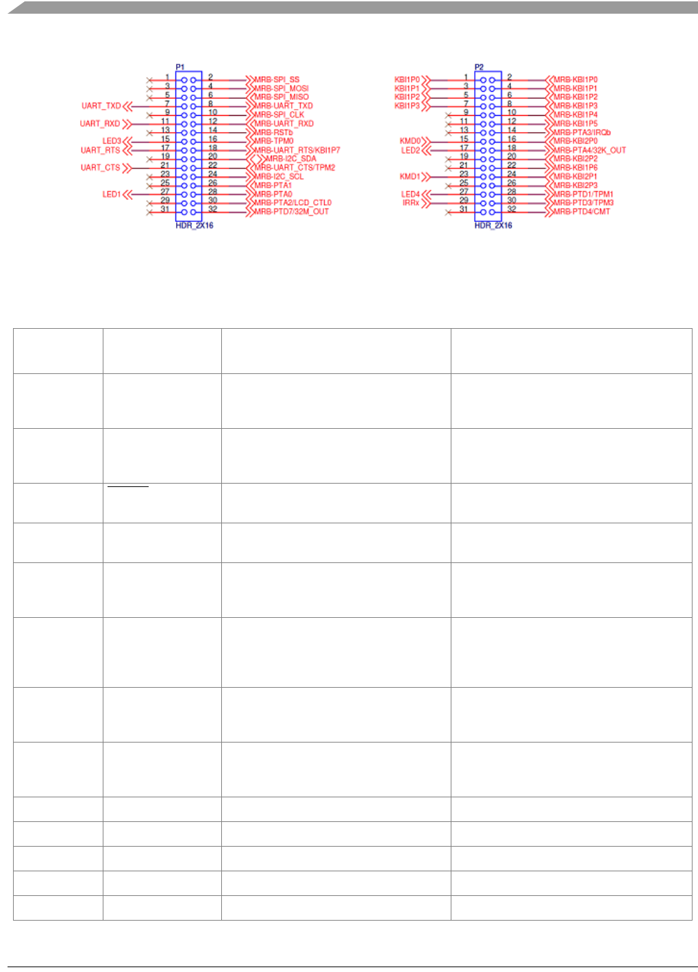
5.2.2 GPIO Connection to 1323x-MRB
IO Connectors J8 and J9 (see Figure 5-1) are receptacles that accept the 1323x-MRB pin headers to mount
the daughtercard. Figure 5-4 shows the 1323x-REM with the 1323x-MRB mounted. Receptacles J8 and
J9 connect to the MC13233 GPIO.
To provide better access and versatility to the GPIO, a secondary set of pin headers P1 and P2 is connected
in series with the IO signals:
• Jumpers must be installed on P1 and P2 to connect 1323x-REM peripherals and functions
• The pin headers provide direct access for connecting custom circuitry to the GPIO
• Power and ground to primary connectors J8 and J9 are not enabled though the pin headers
Figure 5-5 shows IO Header P1 andP2 pin mapping.
1323x Remote Extender Motherboard
1323x Development Hardware Reference Manual, Rev. 1.0
5-8 Freescale Semiconductor
Figure 5-5. 1323x-REM IO Connector J8 and J9 Pin Mapping
Table 5-3 list the P1 and P2 pin header function as it relates to the MC13233.
Table 5-3. 1323x-REM P1 and P2 Pin Header Function Description
1323x-REM
Header Pins
MC13233
Signal Name Description Comments
P1-27, P1-28 PTA0/XTAL_32K Port A Bit 2 / 32.768 kHz oscillator output • Drives LED1; jumper required
• 32.768 kHz oscillator can be enabled on
MRB
P1-26 PTA1/EXTAL_32K Port A Bit 3 / 32.768 kHz oscillator input • Unused
• 32.768 kHz oscillator can be enabled on
MRB
P1-14 RESET Device asynchronous hardware reset.
Active low. Onboard Pullup
• Unused
• Reset signal driven from MRB
P1-30 PTA2 Port A Bit 2. Onboard pullup for TM • Unused
• TM enable; leave unconnected
P2-14 PTA3/IRQ Port A Bit 3 / IRQ. • Unused
• Provides interrupt request input IRQ
(active low)
P2-17, P2-18 PTA4/
XTAL_32KOUT
Port A Bit 4 / Buffered 32.768 kHz clock
output
• Drives LED2; jumper required
• Optional 32.768 kHz output clock for
measuring reference oscillator accuracy
(ppm)
P1-20 PTA5/SDA Port A Bit 5 / IIC Bus data • Unused
• Defaults to open drain for IIC
• Pullup on MRB
P1-24 PTA6/SCL Port A Bit 6 / IIC Bus clock • Unused
• Defaults to open drain for IIC
• Pullup on MRB
P2-1, P2-2 PTB0/KBI1P0 Port B Bit 0 / KBI1 Input Bit 0 REM switch matrix; jumper required
P2-3, P2-4 PTB1/KBI1P1 Port B Bit 1 / KBI1 Input Bit 1 REM switch matrix; jumper required
P2-5, P2-6 PTB2//KBI1P2 Port B Bit 2 / KBI1 Input Bit 2 REM switch matrix; jumper required
P2-7, P2-8 PTB3//KBI1P3 Port B Bit 3 / KBI1 Input Bit 3 REM switch matrix; jumper required
P2-10 PTB4//KBI1P4 Port B Bit 4 / KBI1 Input Bit 4 Unused

1323x Remote Extender Motherboard
1323x Development Hardware Reference Manual, Rev. 1.0
Freescale Semiconductor 5-9
5.2.3 1323x-REM Onboard Peripheral Functions
The 1323x-REM has a simple set of peripheral functions useful to evaluate the MC13233 and to
implement simple node applications, especially a remote control receiver; i.e., interface to host platform.
P2-12 PTB5//KBI1P5 Port B Bit 5 / KBI1 Input Bit 5 Unused
P2-22 PTB6//KBI1P6 Port B Bit 6 / KBI1 Input Bit 6 Unused
P1-17, P1-18 PTB7//KBI1P7 Port B Bit 7 / KBI1 Input Bit 7 • UART flow control RTS input to MCU;
jumper required
• Connects to REM USB <> UART device
P2-15, P2-16 PTC0/KBI2P0 Port C Bit 0 / KBI2 Input Bit 0 REM switch matrix; jumper required
P2-23, P2-24 PTC1/KBI2P1 Port C Bit 1 / KBI2 Input Bit 1 REM switch matrix; jumper required
P2-20 PTC2/KBI2P2 Port C Bit 2 / KBI2 Input Bit 2 Unused
P2-26 PTC3/KBI2P3 Port C Bit 3 / KBI2 Input Bit 3 Unused
P1-10 PTC4/SPICLK Port C Bit 4 / SPI clock • Unused on REM
• Connected to serial FLASH on MRB
P1-2 PTC5/SS Port C Bit 5 / SPI slave select • Unused on REM
• Connected to serial FLASH on MRB
P1-6 PTC6/MISO Port C Bit 6 / SPI MISO • Unused on REM
• Connected to serial FLASH on MRB
P1-4 PTC7/MOSI Port C Bit 7 / SPI MOSI • Unused on REM
• Connected to serial FLASH on MRB
P1- 15, P1-16 PTD0/TPM0 Port D Bit 0 / TPM0 signal Unused
P2-27, P2-28 PTD1/TPM1 Port D Bit 1/ TPM1 signal Drives LED4; jumper required
P1-21, P1-22 PTD2/TPM2 Port D Bit 2 / TPM2 signal • UART flow control CTS output from
MCU; jumper required
• Connects to REM USB <> UART device
P2-29, P2-30 PTD3/TPM3 Port D Bit 3 / TPM3 signal • REM IR receiver input; jumper required
• Drives timer input
P2-32 PTD4/CMT Port D Bit 4/ CMT output • Not used on REM
• Connected to IR blaster on MRB
P1-7, P1-8 PTD6/RXD Port D Bit 6 / UART RXD input • UART RXD input to MCU; jumper
required
• Connects to REM USB <> UART device
P1-11, P1-12 PTD5/TXD Port D Bit 5 / UART TXD output • UART TXD output from MCU; jumper
required
• Connects to REM USB <> UART device
P1-32 PTD7/32MOUT Port D Bit 7 Unused
Table 5-3. 1323x-REM P1 and P2 Pin Header Function Description (continued)
1323x-REM
Header Pins
MC13233
Signal Name Description Comments
1323x Remote Extender Motherboard
1323x Development Hardware Reference Manual, Rev. 1.0
5-10 Freescale Semiconductor
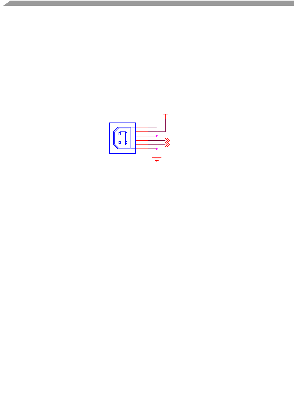
5.2.4 USB Interface
For many applications or demonstrations it is desirable to connect the 1323x-REM to a PC or other device.
A USB port is provided with a USB “B” receptacle plug. The port is connected to a FTDI FT232RQ USB
<> UART device that appears as a Virtual COM port (VCP) to the PC. PC drivers are available with the
module.
The USB interface is configured as a "Bus Powered" device and can draw all required power from the USB
interface. The device is USB 2.0 full speed compatible.
The USB connector is designated as J15. Figure 5-6 shows the connector pinout.
Figure 5-6. USB Connector Pinout
5.2.5 IR Receiver
The 1323x-REM provides an IR receiver that accepts IR signals from the RCM or from any IR based
remote control devices.
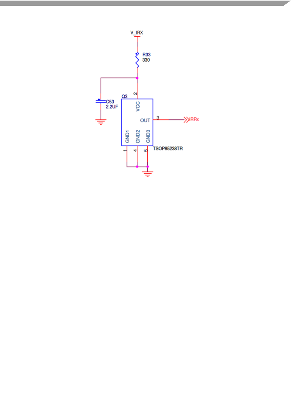
• The IR receiver is the TSOP85238TR device (Q3)
• 38 kHz carrier frequency
• +/- 50 Degree angle of half tranmission distance
• Drives the PTD3/TPM3 signal.
Figure 5-7 shows the IR receiver schematic.
1
2
3
4
S1
S2
1
2
34
+D
-D
G
V
J15
USB_TY PE_B
DATA_P
DATA_M
V_BUS
1323x Remote Extender Motherboard
1323x Development Hardware Reference Manual, Rev. 1.0
Freescale Semiconductor 5-11
Figure 5-7. IR Receiver Circuit
5.2.6 Pushbutton 2x4 Switch Matrix
The1323x-REM provides an 8 pushbutton 2x4 switch matrix for user application input interface.
• The matrix utilizes MC13233 KBI inputs
• All switches have interrupt and device wake up capability
5.2.7 Blue Indicator LEDs
The1323x-REM provides 4 blue LEDs for user application indicator outputs. Refer to Table 5-3 for
listings of the MC13233 outputs that drive the LEDs.
1323x Development Hardware Reference Manual, Rev. 1.0
5-12 Freescale Semiconductor
1323x Remote Extender Motherboard
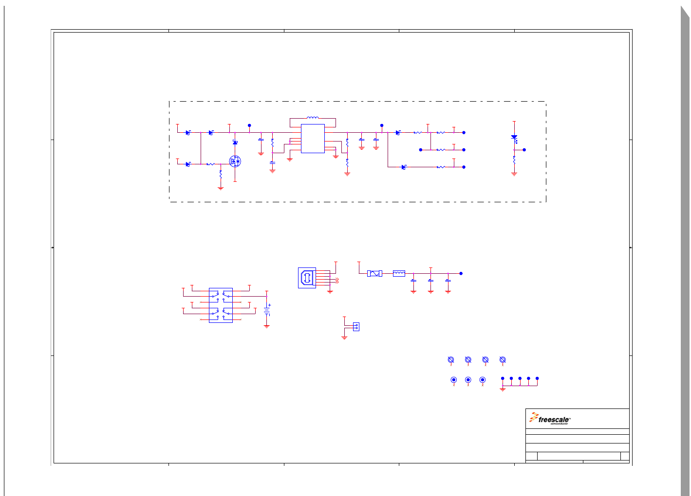
5.3 Schematic, Board Layout, and Bill of Material
Figure 5-8. 1323x-REM Schematic (1 of 2)
5
5
4
4
3
3
2
2
1
1
D D
C C
B B
A A
V_3V6
V_DC
V_LED
V_BHL
V_MRB
V_JACK
V_LED
V_DC
V_SER
V_JACK
V_BUS
V_SER
V_BUS
V_IRX
V_BAT
V_USB VCC
V_BAT
V_USB
V_BUS
V_MAIN
V_SER
DATA_M
DATA_P
Drawing Title:
Size Document Number Rev
Date: Sheet of
Page Title:
ICAP Classification: FCP: FIUO: PUBI:
SCH-26117 PDF: SPF-26117 B
1323X REMOTE EXTENDER MOTHERBOARD
C
Friday, October 02, 2009
POWER MANAGEMENT
44
X______
Drawing Title:
Size Document Number Rev
Date: Sheet of
Page Title:
ICAP Classification: FCP: FIUO: PUBI:
SCH-26117 PDF: SPF-26117 B
1323X REMOTE EXTENDER MOTHERBOARD
C
Friday, October 02, 2009
POWER MANAGEMENT
44
X______
Drawing Title:
Size Document Number Rev
Date: Sheet of
Page Title:
ICAP Classification: FCP: FIUO: PUBI:
SCH-26117 PDF: SPF-26117 B
1323X REMOTE EXTENDER MOTHERBOARD
C
Friday, October 02, 2009
POWER MANAGEMENT
44
X______
POWER ON
EXTERNAL SUPPLY.
NEVER SHUNT!!!
3.3V BUCK/BOOST REGULATOR
TO USE TPS63000,
REPLACE RESISTORS WITH
THE FOLLOWING VALUES:
R45 = 100 OHM, R47 = 1.24M
AND POPULATE R46.
OUTPUT VOLTAGE WILL BE 3.6V
LED
INFRARRED RX
3.3V POWER NETWORK
MODULAR REFERENCE BOARD
R47
0
R47
0
TL2TL2
SL1
4P2T SWITCH
SL1
4P2T SWITCH
1
2
3
4
5
6 7
8
9
10
11
12
TL5TL5
D11
MBR0520LT1G
D11
MBR0520LT1G
TP21TP21
R43
0
R43
0
TP20TP20
1
2
34
+D
-D
G
V
J15
USB_TYPE_B
1
2
34
+D
-D
G
V
J15
USB_TYPE_B
1
2
3
4
S1
S2
C42
10UF
C42
10UF
C43
10UF
C43
10UF
R46
200K
DNP
R46
200K
DNP
TP27TP27
D12
MBR0520LT1G
D12
MBR0520LT1G
F1
0.5A
F1
0.5A
1 2
C41
0.01UF
C41
0.01UF
BH4
125
BH4
125
C33
0.1UF
C33
0.1UF
FID2
FID
FID2
FID
L4
60OHM
L4
60OHM
1 2
BT1
BATTERY HOLDER
BT1
BATTERY HOLDER
12
TL3TL3
Q4
SI2305
Q4
SI2305
1
32
R40
0
R40
0
D13
MBR0520LT1G
D13
MBR0520LT1G
TP29TP29
R36
0
R36
0
D9
MBR0520LT1G
D9
MBR0520LT1G
R45
0
R45
0
BH3
125
BH3
125
TL4TL4
TP25TP25
R39
330
R39
330
C32
10UF
C32
10UF
FID1
FID
FID1
FID
D8
MBR0520LT1G
D8
MBR0520LT1G
BH2
125
BH2
125
LED5
RED
LED5
RED
21
BH1
125
BH1
125
TP19TP19
TP24TP24
J14
HDR 1X2
J14
HDR 1X2
1
2
TL1TL1
R38
4.7K
R38
4.7K
C40
4.7uF
C40
4.7uF
L3 3.3uHL3 3.3uH
1 2
C39
0.1UF
C39
0.1UF
R41
10K
R41
10K
D10
MBR0520LT1G
D10
MBR0520LT1G
FID3
FID
FID3
FID
TP23TP23
U8
TPS63001
U8
TPS63001
EN
6
GND
9
L1
4L2 2
PS/SYNC
7
VOUT 1
VIN
5
VINA
8
FB 10
PGND 3
PPAD 11
R35
0
R35
0
1323x Remote Extender Motherboard
1323x Development Hardware Reference Manual, Rev. 1.0
Freescale Semiconductor 5-13
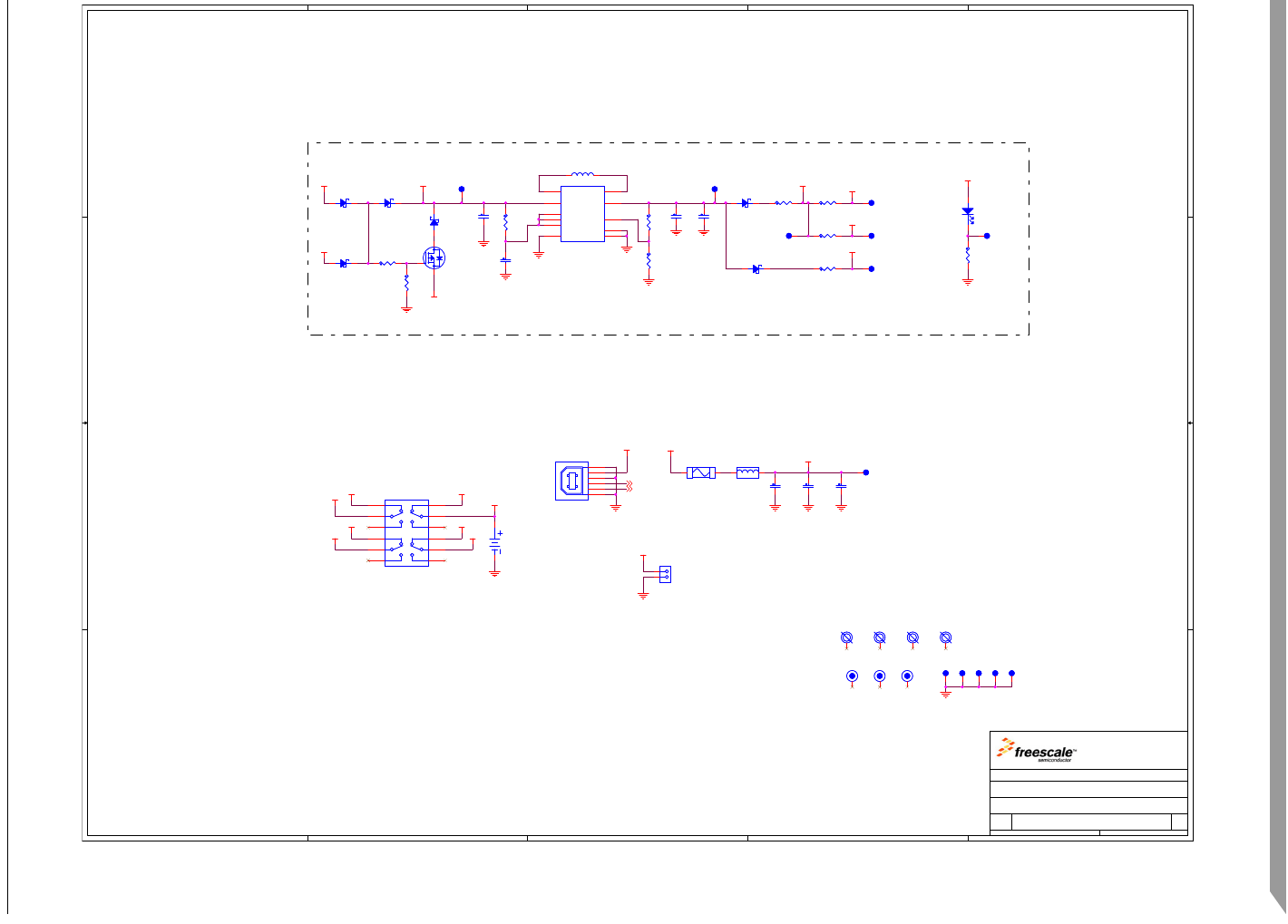
Figure 5-9. 1323x-REM Schematic (2 of 2)
5
5
4
4
3
3
2
2
1
1
D D
C C
B B
A A
V_3V6
V_DC
V_LED
V_BHL
V_MRB
V_JACK
V_LED
V_DC
V_SER
V_JACK
V_BUS
V_SER
V_BUS
V_IRX
V_BAT
V_USB VCC
V_BAT
V_USB
V_BUS
V_MAIN
V_SER
DATA_M
DATA_P
Drawing Title:
Size Document Number Rev
Date: Sheet of
Page Title:
ICAP Classification: FCP: FIUO: PUBI:
SCH-26117 PDF: SPF-26117 B
1323X REMOTE EXTENDER MOTHERBOARD
C
Friday, October 02, 2009
POWER MANAGEMENT
44
X______
Drawing Title:
Size Document Number Rev
Date: Sheet of
Page Title:
ICAP Classification: FCP: FIUO: PUBI:
SCH-26117 PDF: SPF-26117 B
1323X REMOTE EXTENDER MOTHERBOARD
C
Friday, October 02, 2009
POWER MANAGEMENT
44
X______
Drawing Title:
Size Document Number Rev
Date: Sheet of
Page Title:
ICAP Classification: FCP: FIUO: PUBI:
SCH-26117 PDF: SPF-26117 B
1323X REMOTE EXTENDER MOTHERBOARD
C
Friday, October 02, 2009
POWER MANAGEMENT
44
X______
POWER ON
EXTERNAL SUPPLY.
NEVER SHUNT!!!
3.3V BUCK/BOOST REGULATOR
TO USE TPS63000,
REPLACE RESISTORS WITH
THE FOLLOWING VALUES:
R45 = 100 OHM, R47 = 1.24M
AND POPULATE R46.
OUTPUT VOLTAGE WILL BE 3.6V
LED
INFRARRED RX
3.3V POWER NETWORK
MODULAR REFERENCE BOARD
R47
0
R47
0
TL2TL2
SL1
4P2T SWITCH
SL1
4P2T SWITCH
1
2
3
4
5
6 7
8
9
10
11
12
TL5TL5
D11
MBR0520LT1G
D11
MBR0520LT1G
TP21TP21
R43
0
R43
0
TP20TP20
1
2
34
+D
-D
G
V
J15
USB_TYPE_B
1
2
34
+D
-D
G
V
J15
USB_TYPE_B
1
2
3
4
S1
S2
C42
10UF
C42
10UF
C43
10UF
C43
10UF
R46
200K
DNP
R46
200K
DNP
TP27TP27
D12
MBR0520LT1G
D12
MBR0520LT1G
F1
0.5A
F1
0.5A
1 2
C41
0.01UF
C41
0.01UF
BH4
125
BH4
125
C33
0.1UF
C33
0.1UF
FID2
FID
FID2
FID
L4
60OHM
L4
60OHM
1 2
BT1
BATTERY HOLDER
BT1
BATTERY HOLDER
12
TL3TL3
Q4
SI2305
Q4
SI2305
1
32
R40
0
R40
0
D13
MBR0520LT1G
D13
MBR0520LT1G
TP29TP29
R36
0
R36
0
D9
MBR0520LT1G
D9
MBR0520LT1G
R45
0
R45
0
BH3
125
BH3
125
TL4TL4
TP25TP25
R39
330
R39
330
C32
10UF
C32
10UF
FID1
FID
FID1
FID
D8
MBR0520LT1G
D8
MBR0520LT1G
BH2
125
BH2
125
LED5
RED
LED5
RED
21
BH1
125
BH1
125
TP19TP19
TP24TP24
J14
HDR 1X2
J14
HDR 1X2
1
2
TL1TL1
R38
4.7K
R38
4.7K
C40
4.7uF
C40
4.7uF
L3 3.3uHL3 3.3uH
1 2
C39
0.1UF
C39
0.1UF
R41
10K
R41
10K
D10
MBR0520LT1G
D10
MBR0520LT1G
FID3
FID
FID3
FID
TP23TP23
U8
TPS63001
U8
TPS63001
EN
6
GND
9
L1
4L2 2
PS/SYNC
7
VOUT 1
VIN
5
VINA
8
FB 10
PGND 3
PPAD 11
R35
0
R35
0
1323x Remote Extender Motherboard
1323x Development Hardware Reference Manual, Rev. 1.0
5-14 Freescale Semiconductor
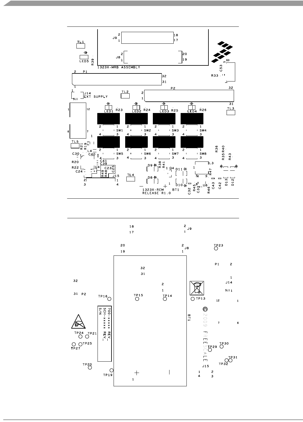
Figure 5-10. 1323x-REM PCB Component Location (Top View)
Figure 5-11. 1323x-REM PCB Test Points
1323x Remote Extender Motherboard
1323x Development Hardware Reference Manual, Rev. 1.0
Freescale Semiconductor 5-15
Figure 5-12. 1323x-REM PCB Layout (Top View)
Figure 5-13. 1323x-REM PCB Layout (Bottom View)
1323x Remote Extender Motherboard
1323x Development Hardware Reference Manual, Rev. 1.0
5-16 Freescale Semiconductor
5.3.1 1323x-REM Bill of Materials
Table 5-4. Bill of Materials
Item Qty. Reference Value Description Mfg. Name Part Number
1 4 BH1, BH2, BH3,
BH4
125 NON-PLATED MOUNTING
HOLE 125 DRILL / 160
KEEPOUT NO PART TO
ORDER
21BT1 BATTERY
HOLDER
BATTERY HOLDER 2XAA TH KEYSTONE
ELECTRONICS
2462
3 2 C23,C24 15PF CAP CER 15PF 50V 5% C0G
0402
KEMET C0402C150J5GAC
4 4 C25,C30,C33,
C39
0.1UF CAP CER 0.1UF 16V 10%
X7R 0402
MURATA GRM155R71C104KA88D
5 3 C32,C42,C43 10UF CAP CER 10UF 10V 10% X7R
0805
Murata GRM21BR71A106KE51L
6 1 C40 4.7uF CAP CER 4.7UF 10V 10%
X5R 0603
TAIYO YUDEN LMK107BJ475KA-T
7 1 C41 0.01UF CAP CER 0.01UF 10V 20%
X7R 0402
AVX 0402ZC103MAT2A
8 1 C53 2.2UF CAP CER 2.2UF 6.3V 20%
X5R 0402
MURATA GRM155R60J225ME15D
9 6 D8,D9,D10,D11
,D12,D13
MBR0520L
T1G
DIODE SCH 0.5A 20V
SOD-123
ON
SEMICONDUCTOR
MBR0520LT1G
10 3 FID1,FID2,FID3 FID FIDUCIAL 060 MIL PAD
W/120 SOLDERMASK AND
040 MIL PAD W/90 MIL
SOLDERMASK NO PART TO
ORDER
GENERIC FID-040
11 1 F1 0.5A FUSE FAST 0.5A 63V SMT
1206
LITTELFUSE 0437.500WR
12 1 J8 CON_2X1
0
CON 2X10 SKT TH 100MIL
CTR 335H AU 104L
SAMTEC SSW-110-01-G-D
13 1 J9 CON_2X9 CON 2X9 SKT TH 100MIL SP
335H AU 194L
SAMTEC SSW-109-02-G-D
14 1 J14 HDR_1X2 HDR 1X2 TH 100MIL SP 375H
AU
TYCO
ELECTRONICS
826629-2
15 1 J15 USB_TYP
E_B
CON 2X2 USB_TYPE_B SKT
RA SHLD TH 2.5MM SP 453H
AU
TYCO
ELECTRONICS
292304-2
16 4 LED1,LED2,LE
D3,LED4
BLUE LED BLUE SGL 20MA SMT
0805
LITE ON LTST-C171TBKT-5A
17 1 LED5 RED LED RED CLEAR SGL 30MA
SMT 0805
LITE ON LTST-C171KRKT
1323x Remote Extender Motherboard
1323x Development Hardware Reference Manual, Rev. 1.0
Freescale Semiconductor 5-17
18 1 L3 3.3uH IND PWR 3.3UH@100KHZ
3.3A 20% SMT
VISHAY
INTERTECHNOLO
GY
IHLP2020BZER3R3M01
19 1 L4 60OHM IND FER BEAD
60OHM@100MHZ 500MA --
0603
MURATA BLM18PG600SN1_
20 2 P1,P2 HDR_2X1
6
HDR 2X16 TH 100MIL CTR
330H AU 100L
SAMTEC TSW-116-07-S-D
21 1 Q3 TSOP8523
8TR
TRAN PHOTO 0.45MA 5.5V
950NM SMT
VISHAY
INTERTECHNOLO
GY
TSOP85238TR
22 1 Q4 SI2305 TRAN PMOS PWR 4.1A 8V
SOT23
VISHAY
INTERTECHNOLO
GY
SI2305ADS-T1-GE3
23 4 R19,R20,R21,R
22
1K RES MF 1.0K 1/16W 5% 0402 VISHAY
INTERTECHNOLO
GY
CRCW04021K00JNED
24 4 R23,R24,R25,R
26
390 RES MF 390 OHM 1/16W 5%
0402
BOURNS CR0402-JW-391GLF
25 2 R33,R39 330 RES MF 330 OHM 1/16W 5%
0402
VISHAY
INTERTECHNOLO
GY
CRCW0402330RJNED
26 6 R35,R36,R40,R
43,R48,R49
0 RES TF ZERO OHM 1/16W
RC0402
VISHAY
INTERTECHNOLO
GY
CRCW04020000ZS
27 1 R38 4.7K RES MF 4.7K 1/16W 5% 0402 SMEC RC73L2Z472JTF
28 1 R41 10K RES MF 10K 1/16W 5% 0402 VISHAY
INTERTECHNOLO
GY
CRCW040210K0JNED
29 1 R45 100 RES MF 100 OHM 1/16W 5%
0402
VISHAY
INTERTECHNOLO
GY
CRCW0402100RJNED
30 1 R46 200K RES MF 200K 1/16W 5% 0402 YAGEO AMERICA RC0402JR-07200KL
31 1 R47 1.24M RES MF 1.24M 1/16W 1%
0402
VISHAY
INTERTECHNOLO
GY
CRCW04021M24FKED
32 1 SL1 4PDT
SWITCH
SW 4PDT SLD TH RA 30V
100MA --
TYCO
ELECTRONICS
1-1437575-1
33 8 SW1,SW2,SW3
,SW4,SW5,SW
6,SW7,SW8
PB switch SW SMT 4.0MM FMS 0.1A
MAX 16V MAX ROHS
COMPLIANT
BOURNS 7914J-1-000E
Table 5-4. Bill of Materials
Item Qty. Reference Value Description Mfg. Name Part Number

1323x Remote Extender Motherboard
1323x Development Hardware Reference Manual, Rev. 1.0
5-18 Freescale Semiconductor
34 15 TP13,TP14,TP1
5,TP16,TP19,T
P20,TP21,TP23
,TP24,TP25,TP
27,TP29,TP30,
TP31,TP32
TPAD_040 TEST POINT PAD 40MIL DIA
SMT, NO PART TO ORDER
NOTACOMPONEN
T
NOTACOMPONENT
35 1 U4 FT232RQ IC XCVR USB TO UART
CTLR 3.3-5.25V QFN32
FUTURE TECH-
NOLOGY
DEVICES INTER-
NATIONAL LTD.
FT232RQ
36 1 U8 TPS6300
1
IC LIN DCDC SYNC 3.3V
OUTPUT 1250-1800KHZ
1.8-5.5V QFN-10
TEXAS INSTRU-
MENTS
TPS63001DRCT
Table 5-4. Bill of Materials
Item Qty. Reference Value Description Mfg. Name Part Number

1323x Development Hardware Reference Manual, Rev. 1.0
Freescale Semiconductor 6-1
Chapter 6
PCB Manufacturing Specifications
This chapter provides the specifications used to manufacture the 1323x Development hardware printed
circuit boards (PCB) described in this manual.
The 1323x Development hardware PCBs must comply with the following:
• The PCB must comply with Perfag10/3C (http://www.perfag.dk/Uk/ukindex.htm)
• The PCB manufacturer’s logo is required
• The PCB production week and year code is required
— The manufacturer’s logo and week/year code must be stamped on the back of the PCB solder
mask
— The PCB manufacturer can not insert text on the PCB either in copper or in silkscreen without
written permission from Freescale Semiconductor, Inc.
• The required Underwriter’s Laboratory (UL) Flammability Rating
— The level is 94V-0 (http://www.ul.com/plastics/flame.html)
— The UL information must be stamped on the back of the PCB solder mask
NOTE
• A complete set of design files is available for the 1323x Development
hardware at the Freescale web site (http:www.freescale.com/802154)
under reference designs. It is recommended that this design or one of a
number of other reference designs be used as a starting point for a
custom application.
• The Freescale IEEE 802.15.4 / ZigBee Package and Hardware Layout
Considerations Reference Manual, (ZHDCRM) is also available at the
same web site to provide additional design guidance.
6.1 Single PCB Construction
This section describes individual PCB construction details.
• The MRB and RCM PCBs are four-layer, multi layer designs
• The REM PCB is a two layer design
• The PCBs contains no blind, buried, or micro vias
• PCB data:
— MRB Size: Approximately 51 x 51mm (2.01 x 2.01 inches)
— RCM Size: Approximately 86 x 178 mm (3.4 x 7.0 inches)
— REM Size: Approximately 79 x 79 mm (3.1 x 3.1 inches)
PCB Manufacturing Specifications
1323x Development Hardware Reference Manual, Rev. 1.0
6-2 Freescale Semiconductor
— MRB, RCM and REM Final thickness (Cu/Cu): 0.34 mm (0.8 inches) +/- 10% (excluding
solder mask)
The following table defines some of the layers of the completed PCB. The artwork identification refers to
the name of the layer in commonly used terms.
The 1323x MRB contains high frequency 2.4 GHz RF circuitry. As a result,
RF component placement, line geometries and layout, and spacing to the
ground plane are critical parameters. As a result, BOARD STACKUP
GEOMETRY IS CRITICAL. Dielectric and copper thicknesses and spacing
must not be changed; follow the stackup (see Figure 6-1) information is
provided with the reference design.
Table 6-1. MRB Layer by Layer Overview
Layer Artwork Identification File Name
1 Silkscreen Top SILK_TOP.art
2 Top Layer Metal TOP.art
3 Ground Layer GND.art
4 Power Layer PWR.art
5 Bottom Layer Metal BOTTOM.art
6 Silkscreen Bottom SILK_BOTTOM.art
Table 6-2. RCM Layer by Layer Overview
Layer Artwork Identification File Name
1 Silkscreen Top SILK_TOP.art
2 Top Layer Metal TOP.art
3 Ground Layer GND.art
4 Power Layer PWR.art
5 Bottom Layer Metal BOTTOM.art
6 Silkscreen Bottom SILK_BOTTOM.art
Table 6-3. REM Layer by Layer Overview
Layer Artwork Identification File Name
1 Silkscreen Top SILK_TOP.art
2 Top Layer Metal TOP.art
3 Bottom Layer Metal BOTTOM.art
4 Silkscreen Bottom SILK_BOTTOM.art

PCB Manufacturing Specifications
1323x Development Hardware Reference Manual, Rev. 1.0
Freescale Semiconductor 6-3
Figure 6-1. MRB PCB Stackup Cross-Section (Four Layer)
• Solder mask is required
• Silk screen is required
6.2 Panelization
The panel size can be negotiated depending on production volume.
6.3 Materials
The PCB composite materials must meet the following requirements:
• Laminate - The base laminate material (laminate) must be FR4. If the laminate material were
changed the RF electrical characteristics may change and degrade RF performance.
• Copper Foil -
— Top and Bottom copper layers must be 1 oz. copper
— Interior layers must be 1/2 oz. copper
• Plating - All pad plating must be Hot Air Levelling (HAL)
6.4 Solder Mask
The solder mask must meet the following requirements:
• Solder mask type: Liquid Film Electra EMP110 or equivalent
• Solder mask thickness: 10 – 30 µm
Dielectric
Dielectric
Dielectric
Metal 1
Metal 2
Metal 3
Metal 4

PCB Manufacturing Specifications
1323x Development Hardware Reference Manual, Rev. 1.0
6-4 Freescale Semiconductor
6.5 Silk Screen
The silk screen must meet the following requirements:
• Silkscreen color: White
• Silkscreen must be applied after application of solder mask if solder mask is required
• The silkscreen ink must not extend into any plated-thru-holes
• The silk screen must be clipped back to the line of resistance
6.6 Electrical PCB Testing
• All PCBs must be 100 percent tested for opens and shorts
• Impedance Measurement - An impedance measurement report is not mandatory
6.7 Packaging
Packaging for the PCBs must be the following requirements:
• Finished PCBs must remain in panel
• Finished PCBs must be packed in plastic bags that do not contain silicones or sulphur materials.
These materials can degrade solderability.
6.8 Hole Specification/Tool Table
See the ncdrill-1-4.tap file included with the Gerber files and the FAB-23451.pdf file.
6.9 File Description
Files included with the download include Design, Gerber and PDF files.
Gerber files are RS-374x format. Not all files included with the Gerber files are for PCB manufacturing.
PDF files included are:
• FAB-2611x.pdf — Board fabrication drawing
• GRB-2611x.pdf — Metal layers, solder mask, solder paste and silk screen
• SPF-2611x.pdf — Schematic
Design files are in Allegro format with OrCAD schematic capture.