Freescale Semiconductor MPC8377EWLAN Wireless Router User Manual MPC837xE RDS User s Guide
Freescale Semiconductor, Inc. Wireless Router MPC837xE RDS User s Guide
Contents
- 1. hardware part
- 2. software part
hardware part

Document Number: MPC837xERDSUG
Rev. 1.0
12/2008
Preliminary, Subject to Change without Notice
MPC837xE-RDS
Reference Design Platform User’s Guide
How to Reach Us:
Home Page:
www.freescale.com
Web Support:
http://www.freescale.com/support
USA/Europe or Locations Not Listed:
Freescale Semiconductor, Inc.
Technical Information Center, EL516
2100 East Elliot Road
Tempe, Arizona 85284
1-800-521-6274 or +1-480-768-2130
www.freescale.com/support
Europe, Middle East, and Africa:
Freescale Halbleiter Deutschland GmbH
Technical Information Center
Schatzbogen 7
81829 Muenchen, Germany
+44 1296 380 456 (English)
+46 8 52200080 (English)
+49 89 92103 559 (German)
+33 1 69 35 48 48 (French)
www.freescale.com/support
Japan:
Freescale Semiconductor Japan Ltd.
Headquarters
ARCO Tower 15F
1-8-1, Shimo-Meguro, Meguro-ku,
Tokyo 153-0064
Japan
0120 191014 or +81 3 5437 9125
support.japan@freescale.com
Asia/Pacific:
Freescale Semiconductor China Ltd.
Exchange Building 23F
No. 118 Jianguo Road
Chaoyang District
Beijing 100022
China
+86 10 5879 8000
support.asia@freescale.com
For Literature Requests Only:
Freescale Semiconductor Literature Distribution
Center
P.O. Box 5405
Denver, Colorado 80217
1-800-441-2447 or +1-303-675-2140
Fax: +1-303-675-2150
LDCForFreescaleSemiconductor@hibbertgroup.com
Information in this document is provided solely to enable system and
software implementers to use Freescale Semiconductor products. There
are no express or implied copyright licenses granted hereunder to design
or fabricate any integrated circuits or integrated circuits based on the
information in this document.
Freescale Semiconductor reserves the right to make changes without
further notice to any products herein. Freescale Semiconductor makes no
warranty, representation or guarantee regarding the suitability of its
products for any particular purpose, nor does Freescale Semiconductor
assume any liability arising out of the application or use of any product or
circuit, and specifically disclaims any and all liability, including without
limitation consequential or incidental damages. “Typical” parameters that
may be provided in Freescale Semiconductor data sheets and/or
specifications can and do vary in different applications and actual
performance may vary over time. All operating parameters, including
“Typicals”, must be validated for each customer application by customer’s
technical experts. Freescale Semiconductor does not convey any license
under its patent rights nor the rights of others. Freescale Semiconductor
products are not designed, intended, or authorized for use as components
in systems intended for surgical implant into the body, or other applications
intended to support or sustain life, or for any other application in which the
failure of the Freescale Semiconductor product could create a situation
where personal injury or death may occur. Should Buyer purchase or use
Freescale Semiconductor products for any such unintended or
unauthorized application, Buyer shall indemnify and hold Freescale
Semiconductor and its officers, employees, subsidiaries, affiliates, and
distributors harmless against all claims, costs, damages, and expenses,
and reasonable attorney fees arising out of, directly or indirectly, any claim
of personal injury or death associated with such unintended or
unauthorized use, even if such claim alleges that Freescale Semiconductor
was negligent regarding the design or manufacture of the part.
Federal Communications Commission Radio Frequency
Interference Statement
This device complies with Part 15 of the FCC rules. Operation is subject to
the following two conditions:
(1) This device may not cause harmful interference and
(2) this device must accept any interference received, including
interference that might cause undesired operation.
Changes or modifications to this equipment not expressly approved by
Freescale could void the user’s authority to operate the equipment.
This equipment has been tested and found to comply with the limits for a
Class B digital device, pursuant to part 15 of the FCC Rules. These limits
are designed to provide reasonable protection against harmful interference
in a residential installation. This equipment generates uses and can radiate
radio frequency energy and, if not installed and used in accordance with
the instructions, may cause harmful interference to radio communications.
However, there is no guarantee that interference will not occur in a
particular installation. If this equipment does cause harmful interference to
radio or television reception, which can be determined by turning the
equipment off and on, the user is encouraged to try to correct the
interference by one or more of the following measures:
—Reorient or relocate the receiving antenna.
—Increase the separation between the equipment and receiver.
—Connect the equipment into an outlet on a circuit different from that to
which the receiver is connected.
—Consult the dealer or an experienced radio/TV technician for help.
Freescale™ and the Freescale logo are trademarks of Freescale
Semiconductor, Inc. All other product or service names are the property of
their respective owners.
© Freescale Semiconductor, Inc. 2009. All rights reserved.
This device has been designed to operate with the attached antennas,
and having a maximum gain of 2.5dBi. Antennas not identical as
that or having a gain greater than 2.5dBi are strictly prohibited
for use with this device. The required antenna impedance is 50 ohms.
To reduce potential radio interference to other users, the antenna
type and its gain should be so chosen that the equivalent
isotropically radiated power (e.i.r.p.) is not more than that
permitted for successful communication.
Reminding
1. The installed antennas must not be located in a manner that
allows exposure of the general population at a distance of
less than 23cm.
2. Mount the antennas in a manner that prevents any personnel
from entering the area within 23cm from the central position
of the antenna.

MPC837xE-RDS, Rev. 1.0
Freescale Semiconductor 3
Preliminary, Subject to Change without Notice
Contents
About This Book
Audience . . . . . . . . . . . . . . . . . . . . . . . . . . . . . . . . . . . . . . . . . . . . . . . . . . . . . . . . . . . . . . . . . . . . 5
Organization . . . . . . . . . . . . . . . . . . . . . . . . . . . . . . . . . . . . . . . . . . . . . . . . . . . . . . . . . . . . . . . . . 5
Definitions, Acronyms, and Abbreviations . . . . . . . . . . . . . . . . . . . . . . . . . . . . . . . . . . . . . . . . . 5
References . . . . . . . . . . . . . . . . . . . . . . . . . . . . . . . . . . . . . . . . . . . . . . . . . . . . . . . . . . . . . . . . . . . 6
Chapters
1 Introduction . . . . . . . . . . . . . . . . . . . . . . . . . . . . . . . . . . . . . . . . . . . . . . . . . . . . . . . . . . . . . . . . . . 7
1.1 Overview . . . . . . . . . . . . . . . . . . . . . . . . . . . . . . . . . . . . . . . . . . . . . . . . . . . . . . . . . . . . . . . . . 7
1.2 Features . . . . . . . . . . . . . . . . . . . . . . . . . . . . . . . . . . . . . . . . . . . . . . . . . . . . . . . . . . . . . . . . . . 7
2 MPC837xE-RDS Board . . . . . . . . . . . . . . . . . . . . . . . . . . . . . . . . . . . . . . . . . . . . . . . . . . . . . . . . 9
2.1 Board-Level Functions . . . . . . . . . . . . . . . . . . . . . . . . . . . . . . . . . . . . . . . . . . . . . . . . . . . . . 10
2.1.1 Reset and Reset Configurations . . . . . . . . . . . . . . . . . . . . . . . . . . . . . . . . . . . . . . . . . . . 10
2.1.2 External Interrupts . . . . . . . . . . . . . . . . . . . . . . . . . . . . . . . . . . . . . . . . . . . . . . . . . . . . . 11
2.1.3 Clock Distribution . . . . . . . . . . . . . . . . . . . . . . . . . . . . . . . . . . . . . . . . . . . . . . . . . . . . . . 12
2.1.4 DDR2 SDRAM Controller . . . . . . . . . . . . . . . . . . . . . . . . . . . . . . . . . . . . . . . . . . . . . . . 13
2.1.5 Local Bus Controller . . . . . . . . . . . . . . . . . . . . . . . . . . . . . . . . . . . . . . . . . . . . . . . . . . . . 14
2.1.6 Flash Memory . . . . . . . . . . . . . . . . . . . . . . . . . . . . . . . . . . . . . . . . . . . . . . . . . . . . . . . . . 15
2.1.7 I2C . . . . . . . . . . . . . . . . . . . . . . . . . . . . . . . . . . . . . . . . . . . . . . . . . . . . . . . . . . . . . . . . . . 15
2.1.8 SATA Controller . . . . . . . . . . . . . . . . . . . . . . . . . . . . . . . . . . . . . . . . . . . . . . . . . . . . . . . 16
2.1.9 PCI Express Interface (PCI-E & Mini PCI-E) . . . . . . . . . . . . . . . . . . . . . . . . . . . . . . . . 16
2.1.10 10/100/1000 BaseT Interface . . . . . . . . . . . . . . . . . . . . . . . . . . . . . . . . . . . . . . . . . . . . . 16
2.1.11 RS-232 Port . . . . . . . . . . . . . . . . . . . . . . . . . . . . . . . . . . . . . . . . . . . . . . . . . . . . . . . . . . . 17
2.1.12 USB 2.0 Interface . . . . . . . . . . . . . . . . . . . . . . . . . . . . . . . . . . . . . . . . . . . . . . . . . . . . . . 17
2.1.13 PCI Subsystem . . . . . . . . . . . . . . . . . . . . . . . . . . . . . . . . . . . . . . . . . . . . . . . . . . . . . . . . 18
2.1.14 COP/JTAG Port . . . . . . . . . . . . . . . . . . . . . . . . . . . . . . . . . . . . . . . . . . . . . . . . . . . . . . . 18
2.2 MPC837xE-RDS Assembly . . . . . . . . . . . . . . . . . . . . . . . . . . . . . . . . . . . . . . . . . . . . . . . . . 20
2.3 Connectors . . . . . . . . . . . . . . . . . . . . . . . . . . . . . . . . . . . . . . . . . . . . . . . . . . . . . . . . . . . . . . 22
2.3.1 COP Connector . . . . . . . . . . . . . . . . . . . . . . . . . . . . . . . . . . . . . . . . . . . . . . . . . . . . . . . . 22
2.3.2 RS-232C Connectors . . . . . . . . . . . . . . . . . . . . . . . . . . . . . . . . . . . . . . . . . . . . . . . . . . . 23
2.3.3 Serial ATA (SATA) Connector . . . . . . . . . . . . . . . . . . . . . . . . . . . . . . . . . . . . . . . . . . . 23
2.3.4 Mini PCI Connector . . . . . . . . . . . . . . . . . . . . . . . . . . . . . . . . . . . . . . . . . . . . . . . . . . . . 23
2.3.5 Power Connector . . . . . . . . . . . . . . . . . . . . . . . . . . . . . . . . . . . . . . . . . . . . . . . . . . . . . . . 24
2.4 LEDs . . . . . . . . . . . . . . . . . . . . . . . . . . . . . . . . . . . . . . . . . . . . . . . . . . . . . . . . . . . . . . . . . . . 24
2.4.1 Power-on LED . . . . . . . . . . . . . . . . . . . . . . . . . . . . . . . . . . . . . . . . . . . . . . . . . . . . . . . . 24
2.4.2 RDS Programmable LEDs . . . . . . . . . . . . . . . . . . . . . . . . . . . . . . . . . . . . . . . . . . . . . . . 24
2.4.3 Ethernet LEDs . . . . . . . . . . . . . . . . . . . . . . . . . . . . . . . . . . . . . . . . . . . . . . . . . . . . . . . . 25
2.5 MPC837xE-RDS Board Configuration . . . . . . . . . . . . . . . . . . . . . . . . . . . . . . . . . . . . . . . . 25
2.5.1 EEPROM . . . . . . . . . . . . . . . . . . . . . . . . . . . . . . . . . . . . . . . . . . . . . . . . . . . . . . . . . . . . 25
2.5.2 PCI Operating Frequency . . . . . . . . . . . . . . . . . . . . . . . . . . . . . . . . . . . . . . . . . . . . . . . . 25

MPC837xE-RDS, Rev. 1.0
4Freescale Semiconductor
Preliminary, Subject to Change without Notice
2.5.3 Reset Configuration Word . . . . . . . . . . . . . . . . . . . . . . . . . . . . . . . . . . . . . . . . . . . . . . . 26
2.5.4 Power Supply . . . . . . . . . . . . . . . . . . . . . . . . . . . . . . . . . . . . . . . . . . . . . . . . . . . . . . . . . 30
2.5.5 Chip-Select Assignments and Memory Map . . . . . . . . . . . . . . . . . . . . . . . . . . . . . . . . . . . . 30
2.6 Specifications . . . . . . . . . . . . . . . . . . . . . . . . . . . . . . . . . . . . . . . . . . . . . . . . . . . . . . . . . . . . 30
2.7 Mechanical Data . . . . . . . . . . . . . . . . . . . . . . . . . . . . . . . . . . . . . . . . . . . . . . . . . . . . . . . . . . 32
3 Board Bootup . . . . . . . . . . . . . . . . . . . . . . . . . . . . . . . . . . . . . . . . . . . . . . . . . . . . . . . . . . . . . . . 32
3.1 Board Jumper Settings . . . . . . . . . . . . . . . . . . . . . . . . . . . . . . . . . . . . . . . . . . . . . . . . . . . . . 33
3.2 External Connections . . . . . . . . . . . . . . . . . . . . . . . . . . . . . . . . . . . . . . . . . . . . . . . . . . . . . . 34
4 MPC837xE-RDS Software . . . . . . . . . . . . . . . . . . . . . . . . . . . . . . . . . . . . . . . . . . . . . . . . . . . . . 34
4.1 Application Features for MPC837xE-RDS reference software . . . . . . . . . . . . . . . . . . . . . . 34
4.2 Application Connections . . . . . . . . . . . . . . . . . . . . . . . . . . . . . . . . . . . . . . . . . . . . . . . . . . . . 36
5 Unit Assembly . . . . . . . . . . . . . . . . . . . . . . . . . . . . . . . . . . . . . . . . . . . . . . . . . . . . . . . . . . . . . . 37
5.1 Assembling the Enclosure and Board Assembly . . . . . . . . . . . . . . . . . . . . . . . . . . . . . . . . . 37
5.2 Attaching a Wi-Fi Card to the Product . . . . . . . . . . . . . . . . . . . . . . . . . . . . . . . . . . . . . . . . . 37
5.3 Attaching a SATA hard disk to the Product . . . . . . . . . . . . . . . . . . . . . . . . . . . . . . . . . . . . . 37

MPC837xE-RDS, Rev. 1.0
Freescale Semiconductor 5
Preliminary, Subject to Change without Notice
About This Book
This document presents system architecture, board-level functions, external connections, and software
features for the MPC837xE-RDS board. It provides guidance of how to operate this product, making it
easy for the user to connect with the outside world. The front part of this book focuses primarily on the
board and functions. The latter part of the book focuses on the mechanical aspects.
Audience
Users who want to become familiar with the MPC837xE-RDS board, its characteristics, and how to
program the device.
Organization
Chapter 1, Introduction, describes the features and block diagram for the MPC837xE-RDS board.
Chapter 2, MPC837xE-RDS Board, describes the board in terms of its hardware: board-level functions,
connectors, configurations, and board mechanical data.
Chapter 3, Board Bootup, describes the board settings and physical connections needed to boot the
MPC837xE-RDS board.
Chapter 4, MPC837xE-RDS Software, describes the main software features for MPC837xE-RDS board.
Definitions, Acronyms, and Abbreviations
The following list defines the acronyms and abbreviations used in this document.
NAS Network-Attached Storage
RAID Redundant Array of Inexpensive Disks
CPU Central Processing Unit
PoE Power over Ethernet
DDR2 SDRAM Double-Data-Rate Two Synchronous Dynamic Random Access Memory
NOR Flash Nor Gate Flash
eTSEC Enhanced Three-Speed Ethernet Controller
RGMII Reduced Gigabit Media Independent Interface
WAN Wide Area Network
LAN Local Area Network
USB Universal Serial Bus
ULPI USB Low-Pin Count Interface
SATA Serial Advanced Technology Attachment (computer bus)
PCI Peripheral Component Interconnect (computer bus)
PCI-E Peripheral Component Interconnect Express (computer bus)
SDHC Secure Digital High Capacity (SD 2.0 memory card)

MPC837xE-RDS, Rev. 1.0
6Freescale Semiconductor
Preliminary, Subject to Change without Notice
I2C Inter-Integrated Circuit (computer bus)
EEPROM Electrically Erasable Programmable Read-Only Memory
JTAG Joint Test Action Group
DHCP Dynamic Host Configuration Protocol
DNS Domain Name System
VLAN Virtual Local Area Networks
NAT Network Address Translation
PAT Port Address Translation
RIP Routing Information Protocol
VRRP Virtual Router Redundancy Protocol
PPPoE Point-to-Point Protocol over Ethernet
IGMP Internet Group Management Protocol
UPnP Universal Plug and Play (computer protocol)
SNMP Simple Network Management Protocol
QoS Quality of Service
IPsec Internet Protocol Security
PPTP Point-to-Point Tunneling Protocol
L2TP Layer 2 Tunneling Protocol
References
The following sources were referenced to produce this book:
•MPC8379E PowerQUICC™ II Pro Integrated Host Processor Family Reference Manual
(MPC8379ERM)
•MPC8379E PowerQUICC II Pro Integrated Host Processor Hardware Specifications
(MPC8379EEC
•Hardware and Layout Design Considerations for DDR Memory Interfaces (AN2582)

Introduction
MPC837xE-RDS, Rev. 1.0
Freescale Semiconductor 7
Preliminary, Subject to Change without Notice
1Introduction
This section presents the features and block diagram for the MPC837xE-RDS board.
1.1 Overview
The MPC837xE-RDS is a reference design based on the MPC8377E PowerQUICCTMII Pro processor. It
supports applications of Wi-Fi Router, DMS (Digital Media Server), NAS with RAID, or Office in BOX,
etc. The documentation for manufacturing the MPC837xE-RDS—including schematic, Gerber files,
reference software, Bill Of Material (BOM)—is on the product CD. With the documentation, original
equipment manufacturers (OEMs) and original design manufacturers (ODMs) can accelerate the
development process and speed time-to-market for their real product.
1.2 Features
This section presents the features, specification, and block diagram of the MPC837xE-RDS board. The
features are as follows:
•CPU
— Freescale MPC8377E @ 667 MHz
•Power
— PoE power solution based on LM5072 up to 30 W output, designed as one daughter
module board
— 48 V DC input used as the alternative power source when PoE is not available
• Memory subsystem
— On-board 512-MByte DDR2 unbuffered SDRAM
— 64-MByte NOR Flash
• Interfaces
— 10/100/1000 BaseT Ethernet ports
– eTSEC1
– RGMII interface: WAN, 1 x 10/100/1000 BaseT with RJ-45 interface, using
RealtekTM RTL8211B single port 10/100/1000 BaseT PHY. This port
supports PoE feature
– eTSEC 2
– RGMII interface: LAN, 1 x 10/100/1000 BaseT with RJ-45 interface, using
RealtekTM RTL8211B single port 10/100/1000 BaseT PHY
— USB 2.0 Host
– ULPI interface: 1 x USB 2.0 Type A Receptacle interface, using SMSCTM
USB3300 Hi-Speed USB PHY
— Serial ATA Controller

MPC837xE-RDS, Rev. 1.0
8Freescale Semiconductor
Preliminary, Subject to Change without Notice
Introduction
– Two standard External SATA connectors
— PCI: 32-bit PCI interface up to 66 Mhz
– 2x 32-bit 3.3 V mini PCI slots
— PCI Express
– Two mini PCI Express Connectors, or
– One mini PCI Express connector and one PCI Express x1 connector
—SDHC
– One SDHC Card Connector
—I
2C
–I
2C connected to ST M24256 Serial EEPROM
— Board Connectors
– One DC power jack
– One internal 2 x 5 RS-232 connector
– JTAG / COP for debugging
— Form factor
– Mini ITX form factor (170 mm x 170 mm, or 6693 mils x 6693 mils)
• 6-layer PCB (4 layers signals and separate power and ground layers)
• Certification
—CE/FCC
• Lead-Free (RoHS)
MPC837xE-RDS Board
MPC837xE-RDS, Rev. 1.0
Freescale Semiconductor 9
Preliminary, Subject to Change without Notice
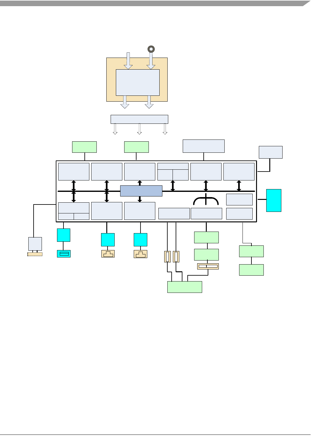
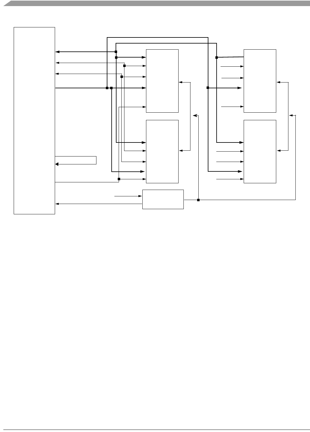
Figure 1 shows the MPC837xE-RDS board block diagram.
Figure 1. MPC837xE-RDS Board Block Diagram
2 MPC837xE-RDS Board
This section presents the board-level functions, specifications, and mechanical data for the
MPC837xE-RDS board.
e 300 Core
32 KB
D-Cache
DUART
Dual I2C
Timers
GPIO, SPI
Interrupt
Controller
Security DDR
Controller Local Bus
USB
Hi-Speed
Host Device
PHY
ULPI RGMII RGMII
RTL8211
Nor Flash
(x 16)
PCI
DDR2 (x64)
I2C1
PHY
UART1
DDR2
MPC8377E
PCI-E
SATAII
eSATA
con
PCI
SD
miniPCI
Socket
miniPCI
Socket
SD
Card
Clock Gen
PCI- E 1X
JTAG/COP
RTL8211 PHY PHY
EEPROM
miniPCI-E
Socket
miniPCI-E
Socket
USB Type A
LM5072
48V PoE 48V AC/DC
1.8 1.5 1.0
5V 3.3V
PoE
Card
32 KB
I-Cache
10/100/1000
Ethernet
eTSEC1
10/100/1000
Ethernet
eTSEC2
MPC837xE-RDS, Rev. 1.0
10 Freescale Semiconductor
Preliminary, Subject to Change without Notice
MPC837xE-RDS Board
2.1 Board-Level Functions
The board-level functions discussed in this section are reset, interrupts, clock distribution, and interface
specification.
2.1.1 Reset and Reset Configurations
The MPC837xE-RDS reset module generates a single reset to reset the MPC837xE and other peripherals
on the board. The reset unit provides power-on reset, hard reset, and soft reset signals in compliance with
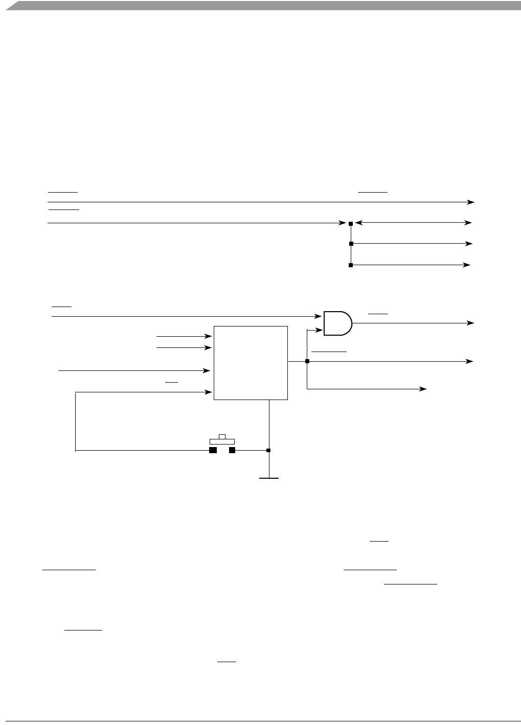
the MPC837xE hardware specification. Figure 2 shows the reset circuitry.
Figure 2. Reset Circuitry of the MPC837xE
• The COP/JTAG port or the MPC837xE generates the signal for hard reset.
• The Maxim MAX6829 device generates the power-on reset. When MR is de-asserted and 3.3 V is
ready, the MAX6829 internal timeout guarantees a minimum reset active time of 140 ms before
PORESET is de-asserted. This circuitry guarantees a 140 ms PORESET pulse width after 3.3 V
reaches the right voltage level, and this meets the specification of the PORESET input of
MPC837xE.
• The COP/JTAG port reset provides convenient hard-reset capability for a COP/JTAG controller.
The RESET line is available at the COP/JTAG port connector. The COP/JTAG controller can
directly generate the hard-reset signal by asserting this line low.
• The pushbutton reset interfaces the MR signal with a debounce capability to produce a manual
master reset of the processor.
MAX6829
3.3 V
Push Button
HRESET from COP
SRESET from COP
TRST from COP
SRESET to MPC837xE
PORESET to MPC837xE
FLASH
10/100/1000 PHY
MPC837xE
TRST to MPC837xE
GND
1.0 V
MR
Watchdog Input from MPC837xE
PCI-E & Mini PCI-E
MPC837xE-RDS Board
MPC837xE-RDS, Rev. 1.0
Freescale Semiconductor 11
Preliminary, Subject to Change without Notice
• The COP/JTAG port also generates the soft reset for the system. Assertion of SRESET causes the
MPC837xE to abort all current internal and external transactions and set most registers to their
default values.
2.1.2 External Interrupts
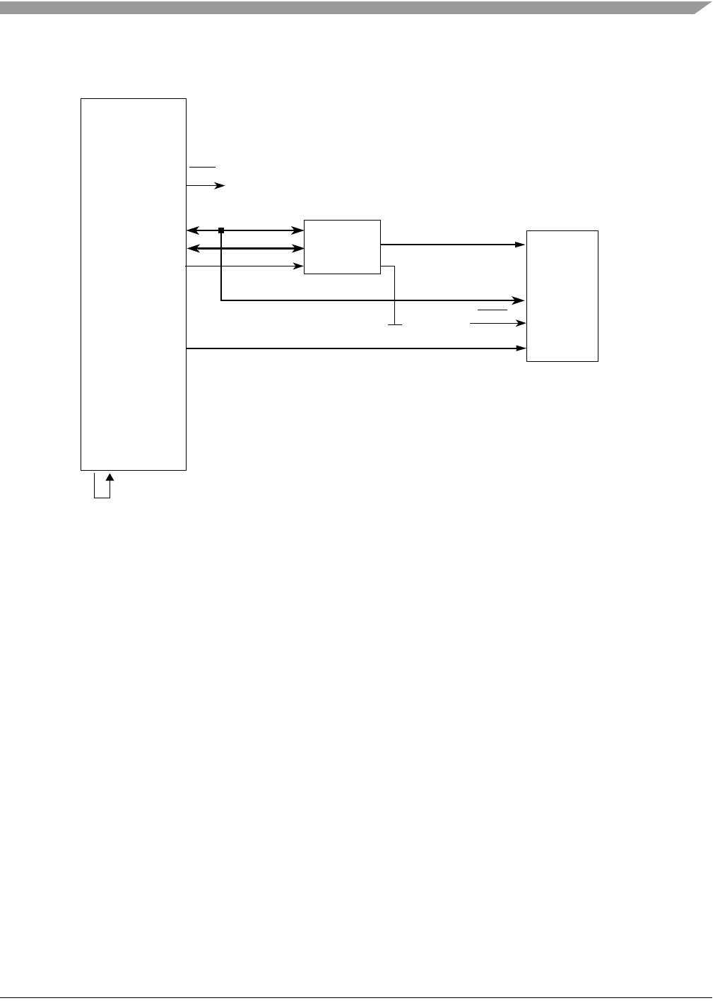
Figure 3 shows the external interrupt circuitry to the MPC837xE.
Figure 3. MPC837xE Interrupt Circuitry
The following items describe the interrupt signals shown in Figure 3:
• PHY interrupt (TSEC1_IRQ, TSEC2_IRQ). Two RTL8211B GBE PHY interrupts are connected
to IRQ1 and IRQ2 of the MPC837xE. The system software can detect the status of the Ethernet
link and the PHY internal status.
• SD Card Write Protect interrupt (SD_WP). The SD card socket has a mechanical pin that can
indicate whether the SD card inserted is write-protected or not. It is connected to IRQ4 of the
MPC837xE.
• PCI interrupt (PCI_INTA, PCI_INTB). Two mini PCI slots INTA and INTB drive IRQ5 and IRQ6
of the MPC837xE, respectively
TSEC1_IRQ
SD_WP
PCI_INTA
PCI_INTB
IRQ1
IRQ2
IRQ3
IRQ4
IRQ5
IRQ6
IRQ7
MPC837xE
External Logic
IRQ0
TSEC2_IRQ
MPC837xE-RDS, Rev. 1.0
12 Freescale Semiconductor
Preliminary, Subject to Change without Notice
MPC837xE-RDS Board
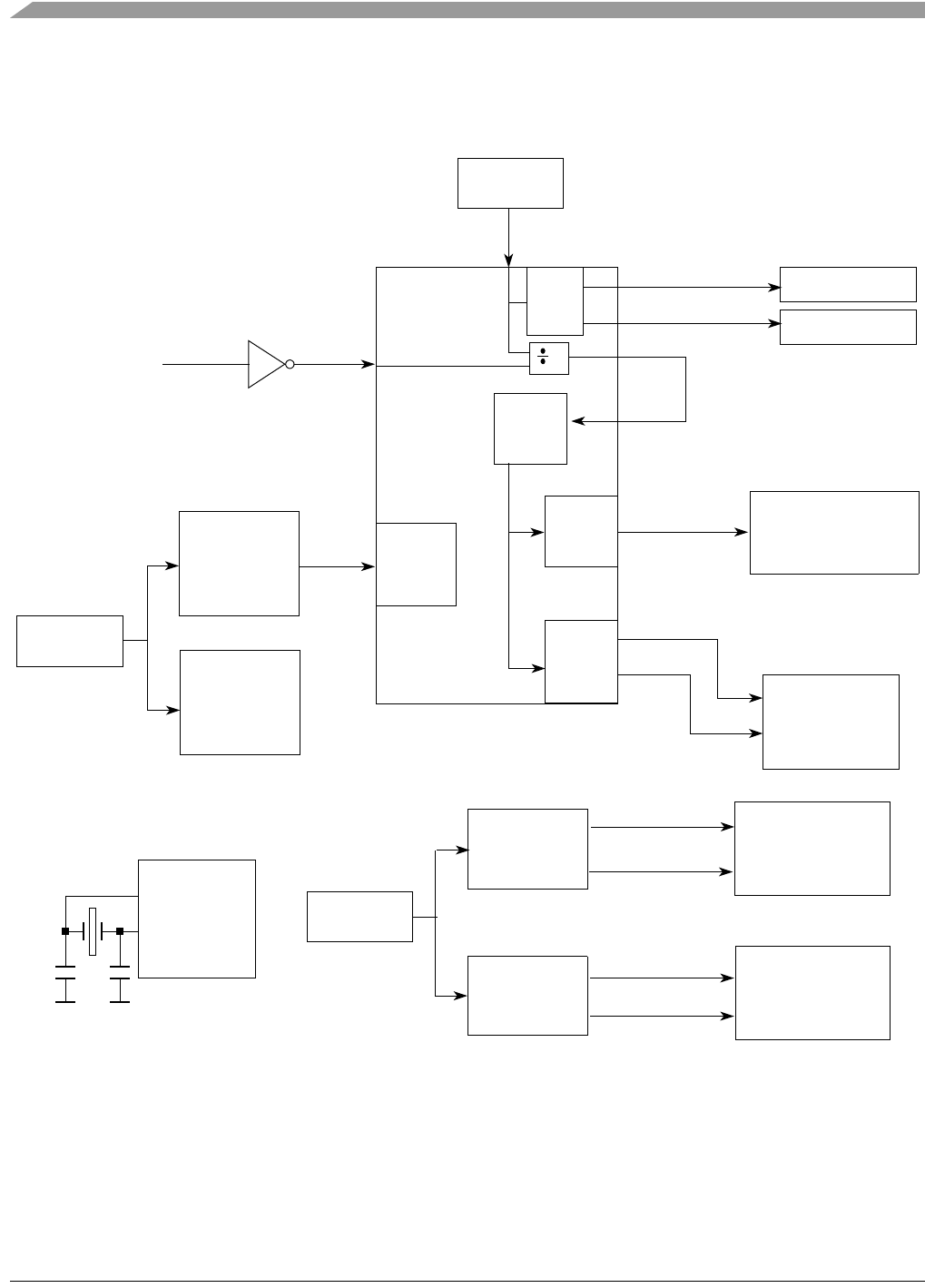
2.1.3 Clock Distribution
Figure 4 and Table 1 show the clock distribution on the MPC837xE-RDS board.
Figure 4. MPC837xE-RDS Clock Distribution Diagram
MPC837xE
Local Bus CLK
DDR2 SDRAM
LCLKx
MCKx
MCKx
200 MHz
50 MHz to 133 MHz
eTSEC
local bus
DLL
DDR
DLL
PCI
DIV
66.666 MHz
OSC
CLKIN
33/66 MHz
33/66 MHz
Mini PCI Slot
Mini PCI Slot
OCCR
2
PCI_SYNC_OUT
PCI_SYNC_IN
System
PLL
CFG_CLKIN_DIV
USB3300
GND GND
24 MHz
Crystal
25 MHz
OSC
RTL8211B
RTL8211B
M66EN
CLK (DDR400)
125 MHz
25 MHz
OSC
PI6C557-03
PI6C557-03
SD_REF_CLKx
SD_REF_CLKx
PCIE_CLKx
PCIE_CLKx
100 MHz
SerDes Interface
100 MHz
Mini PCI-e or
PCI-e x1 Interface

MPC837xE-RDS Board
MPC837xE-RDS, Rev. 1.0
Freescale Semiconductor 13
Preliminary, Subject to Change without Notice
2.1.4 DDR2 SDRAM Controller
MPC837xE uses DDR2 SDRAM as the system memory. The DDR2 interface uses the SSTL2
driver/receiver and 1.8 V power. A Vref 1.8V/2 is needed for all SSTL2 receivers in the DDR2 interface.
For details on DDR timing design and termination, refer to the Freescale application note entitled
Hardware and Layout Design Considerations for DDR Memory Interfaces (AN2582). Figure 5 shows the
DDR SDRAM controller connection.
Table 1. Clock Distribution
Clock Frequency Module Generated by Description
66.666 MHz MPC837xE CLKIN 66.666 MHz oscillator The MPC837xE uses CLKIN to generate the
PCI_SYNC_OUT clock signal, which is fed back to
the internal system PLL through the PCI_SYNC_IN
signal. From the power-on reset configuration, the
internal PLL generates the CSB clock, which is fed to
the e300 core PLL for generating the e300 core clock.
The PCI M66EN pin is inverted for
CFG_CLKIN_DIV configuration input, which
selects whether the PCI_SYNC_OUT signal is
CLKIN or CLkIN/2.
125 MHz MPC837xE eTSEC RTL8211B The gigabit Ethernet PHY (RTL8211B) provides a
125-MHZ clock for eTSEC operation.)
200 MHz DDR2 SDRAM MPC837xE The DDR memory controller is configured to use the
1:1 mode CSB to DDR clock for the DDR interface.
The local bus clock uses CCB/n clock, where n is
configured from the LCRR register.
25 MHz GBE PHY (RTL8211B) 25 MHz oscillator The 25 MHz oscillator generates the clock for
RTL8211B.
33/66 MHz Mini PCI slot MPC837xE The PCI module uses the PCI_SYNC_IN as its clock
source. The trace of the PCI_SYNC_IN/
PCI_SYNC_OUT signal is synchronized with all the
PCI signals of the PCI slots.
24 MHz USB PHY (USB3300) 24 MHz crystal
100 MHz SerDes Interface 25 MHz oscillator and
PI6C557-03 clock
generator
The SerDes reference clock uses 100 MHz.
100 MHz Mini PCI-e and PCI-e x1
Interface
25 MHz oscillator and
PI6C557-03 clock
generator
MPC837xE-RDS, Rev. 1.0
14 Freescale Semiconductor
Preliminary, Subject to Change without Notice
MPC837xE-RDS Board
Figure 5. DDR2 SDRAM Connection
2.1.5 Local Bus Controller
The MPC837xE local bus controller has a 32-bit LAD[0–31] address that consists of data multiplex bus
and control signals. The local bus speed is up to 133 MHz. To interface with the standard memory device,
an address latch must provide the address signals. The LALE is used as the latching signal. To reduce the
load of the high speed 32-bit local bus interface, there is a data buffer for all low-speed devices attached
to the memory controller. The local bus only drives the 64MB NOR Flash menory on the MPC837xE-RDS
board:
DDR2
SDRAM
Controller
Vref
Generator
Vref 0.9 V
1.8 V Input Vref
MSYNC_OUT
MSYNC_IN
MPC837xE
DDR2
SDRAM
Vref
Vref
DQ[0:63]
DQ[32:47]
DQ[0:15]
DM[0:7] DM[0,1]
DM[4,5]
DQS[0:7] DQS[0,1]
DQS[4,5]
A[0:12], BA[0:2],CTRL
MCK[0:3] pairs
MCK0
MCK2 pair
DDR2
SDRAM
DDR2
SDRAM
DQ[48:63]
DQ[16:31]
DM[2,3]
DM[6,7]
DQS[2,3]
DQS[6,7]
MCK1 pair
MCK3 pair
DDR2
SDRAM
Vref
Vref
1Gb(X16) 1Gb(X16)
1Gb(X16) 1Gb(X16)
pair
MPC837xE-RDS Board
MPC837xE-RDS, Rev. 1.0
Freescale Semiconductor 15
Preliminary, Subject to Change without Notice
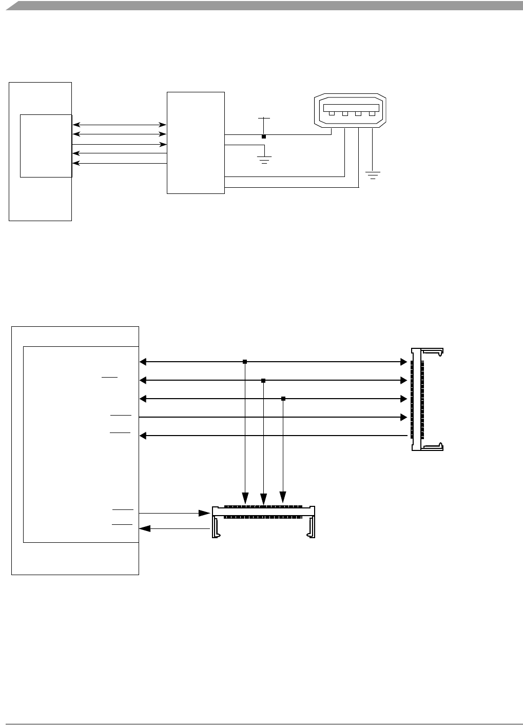
Figure 6 shows the block diagram and connections for the local bus.
Figure 6. Local Bus Connections
2.1.6 Flash Memory
MPC837xE-RDS provides 64Mbytes NOR Flash memory using general-purpose chip-select machine
(GPCM). The NOR Flash is 16-bit port size in the system. It is selected as the boot Flash when J12 pins 2
and 3 are jumpered together.
2.1.7 I2C
The MPC837xE has two I2C interfaces. On the MPC837xE-RDS board, the MPC837xE serves as I2C
master for both I2C buses (I2C1 and I2C2). I2C1 is connected to the following:
• Serial EEPROM M24256 at address 0x50.
• PCI-E and mini PCI-E socket.
The M24256 serial EEPROM can store the reset configuration word of the MPC837xE, as well as store
the configuration registers values if the boot sequencer of MPC837xE is enabled. The I2C address of the
M24256 EEPROM on I2C1 bus is 0x50.
A[24:0]
CS
S29GL512N
NOR Flash (16-bit)
MPC837xE
LAD[0:31]
BADDR[27:30]
D[15:0]
LALE
Address
LE
Local Bus
LCS0
Control
OE
D[0:15]
A[6:30]
LCS0
Latch
LCS0
Control
LAD[6:26]
LAD[0:15]
Controller
GND
Control Signals
LSYNC_OUT
LSYNC_IN
LCKE
LCLK0
LCLK1
MPC837xE-RDS, Rev. 1.0
16 Freescale Semiconductor
Preliminary, Subject to Change without Notice
MPC837xE-RDS Board
2.1.8 SATA Controller
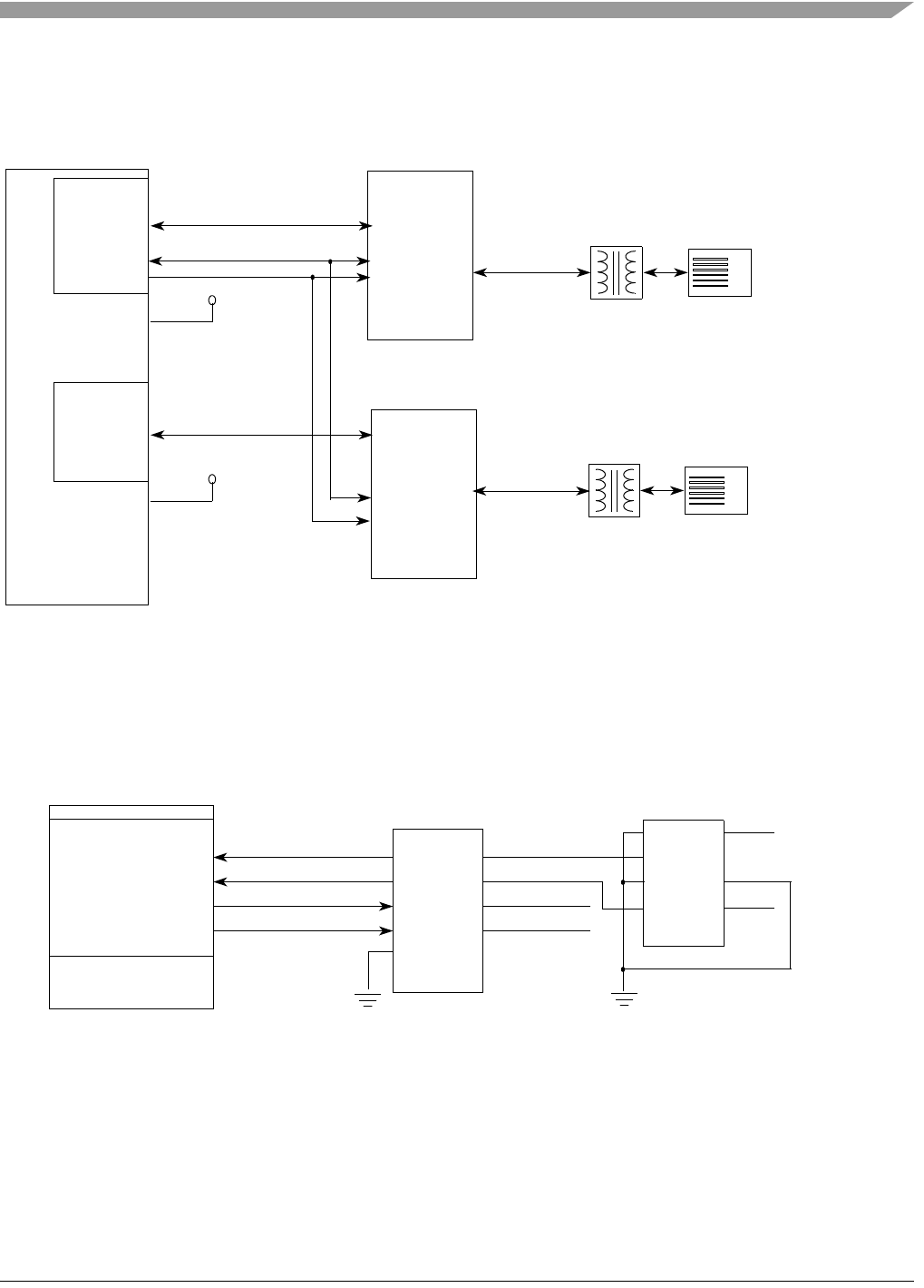
MPC837xE has a SATA controller for storage applications as shown in Figure 7. There are two SATA
channels for MPC8377E. It requires a 100-MHz input clock, which is provided by the clock generator.
2.1.9 PCI Express Interface (PCI-E & Mini PCI-E)
MPC8377E supports the PCI Express (PCI-E) interface. It can be configured as two mini PCI-E interfaces
or one mini PCI-E interface and one 1X PCI-E interface as shown in Figure 7. It also requires a 100-MHz
input clock, which is provided by the clock generator.
Figure 7. SATA and PCI-E Connections
2.1.10 10/100/1000 BaseT Interface
On the MPC837xE-RDS board, eTSEC1 and eTSEC2 use RGMII mode. The eTSEC1 and eTSEC2 drive
two on-board 10/100/1000 PHYs (RTL8211B), respectively. The I/O voltage is set to 3.3 V RGMII for
RTL8211B. The RGMII (1000 BaseT) is a source synchronous bus. For a transmit bus connection, it is
synchronous to GTX_CLK from the TSEC module. The receive bus connection is synchronous to
RX_CLK generated from the PHY device. The MPC837xE MII management interface also connects to
MPC8377E
SATA
eSATA Channel
eSATA Channel
PCI-E (1X)
Mini PCI-E
& PCI-E
Or
Mini PCI-E
MPC837xE-RDS Board
MPC837xE-RDS, Rev. 1.0
Freescale Semiconductor 17
Preliminary, Subject to Change without Notice
the RTL8211B. Figure 8 shows the connection between the MPC837xE eTSEC1 and eTSEC2 to the
RTL8211B.
Figure 8. RGMII Interface Connection for 10/100/1000 BaseT Ethernet
2.1.11 RS-232 Port
Figure 9 illustrates the serial port connection using a SP3232 3.3 V RS-232 driver to interface with a 2 x
5 Header. This serial connection runs at up to 115.2 Kbps.
Figure 9. UART Debug Port Connection
2.1.12 USB 2.0 Interface
The MPC837xE has a internal USB modules (dual-role (DR) module). On the MPC837xE-RDS board, it
connects to the USB PHY (USB3300) through the 8-bit UTMI low-pin-count interface (ULPI). The
RJ-45
eTSEC1
MPC837xE
RTL8211B
MDIO
MDC
EC_MDIO
EC_MDC
RGMII interface
PHY addr = 0x02
eTSEC2
3.3 V
LVDD2
RJ-45
(Enet0, supports PoE)
(Enet1)
3.3 V
LVDD1
RGMII interface RTL8211B
MDIO
MDC
PHY addr = 0x03
SP3232
TXD
RXD
CTS
RX
TX
TX
DO
DI
DI
MPC837xE
RTS
RS-232
Serial
Port
RXRXD
RTS
TXD
CTS
DO
UART0
4
6
8
3
7
5
2
1
910
TXD
RTS
MPC837xE-RDS, Rev. 1.0
18 Freescale Semiconductor
Preliminary, Subject to Change without Notice
MPC837xE-RDS Board
USB3300 PHY connects to a Type A receptacle connector that serves as a host interface. Figure 10 shows
the connection of USB.
Figure 10. USB Port Connections
2.1.13 PCI Subsystem
The MPC837xE has PCI interfaces. It connects to two 32-bit 3.3 V mini PCI slots, as shown in Figure 11.
Figure 11. PCI Subsystem
2.1.14 COP/JTAG Port
The common on-chip processor (COP) is part of the MPC837xE JTAG module and is implemented as a
set of additional instructions and logic. This port can connect to a dedicated emulator for extensive system
debugging. Several third-party emulators in the market can connect to the host computer through the
MPC837xE
ULPI_D[7:0]
ULPI_STP
ULPI_NXT
ULPI_CLK
DIR
USB3300
D[7:0]
STP
NXT
CLKOUT
ULPI_DIR VBUS
DM
ID
5V
DP
USB_TYPE_A_RECEPTACLE
MPC837xE
32-Bit PCI
PCI-AD[0:31]
PCI-CBE[0:3]
PCI-REQ0
PCI-GNT0
PCI-CTRL 32-Bit 3.3 V
Mini PCI Slot
32-Bit 3.3 V
Mini PCI Slot
PCI-REQ1
PCI-GNT1
AD15
AD14
MPC837xE-RDS Board
MPC837xE-RDS, Rev. 1.0
Freescale Semiconductor 19
Preliminary, Subject to Change without Notice
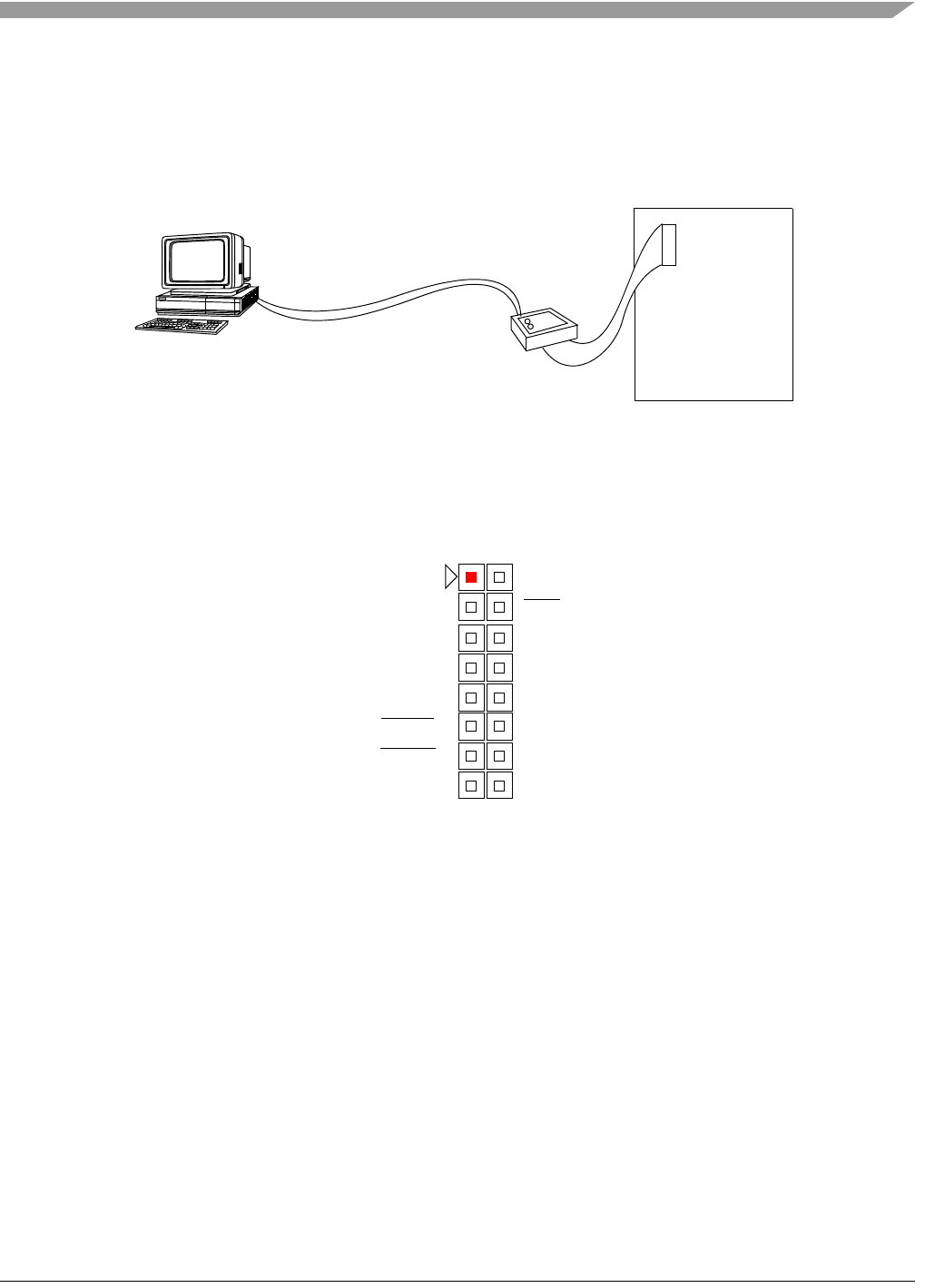
Ethernet port, USB port, parallel port, RS-232, etc. Figure 12 shows a typical setup using a USB port
emulator.
Figure 12. Connecting the MPC837xE-RDS Board to a Parallel Emulator
The 16-pin generic header connector carries the COP/JTAG signals and the additional signals for system
debugging. Figure 13 shows the connector pinout.
Figure 13. MPC837xE-RDS Board COP Connector
PC
MPC837xE-RDS
J4
USB
Emulator
TDI
Pull-up
TCK
TMS
SRESET
HRESET
CKSTP_OUT
GND
TRST
Pull-up
NC
NC
GND
1
TDO
NC
NC
MPC837xE-RDS, Rev. 1.0
20 Freescale Semiconductor
Preliminary, Subject to Change without Notice
MPC837xE-RDS Board
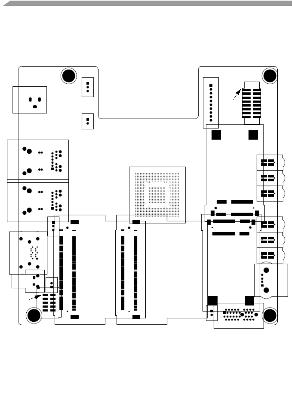
2.2 MPC837xE-RDS Assembly
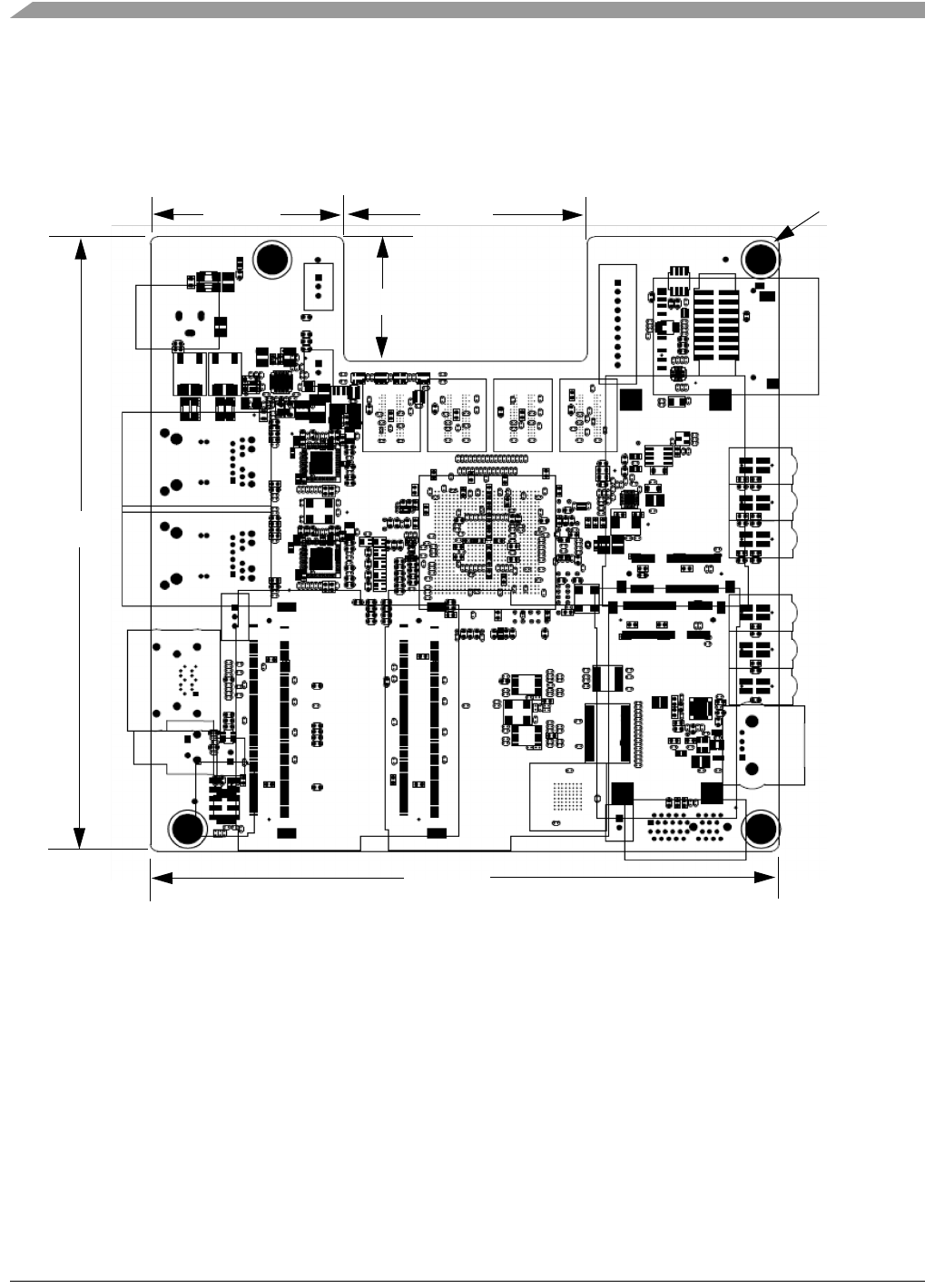
Figure 14 shows the MPC837xE-RDS board top view, with the references of LEDs, jumpers, headers, and
switches.
Figure 14. MPC837xE-RDS Top View
CAUTION
Use 3.3 V mini PCI cards only for mini PCI slots. Power down before
insertion or removal.
48 V DC Power
J13
J15
J14
P1 WAN (supports PoE)
P2 LAN
MPC837xE
JP1 J4
COP Connector
Pin 1
J12
eSATA
J16
SW1
Reset
J7
J6
RS232 COM1
P3
Mini PCI (Top)
P4
Mini PCI (Bottom)
P5
Mini PCI-E
P6
Mini PCI-E
J10 P7
PCI-E (1x)
J5
USB
D7
D8
D9
Pin 1
D14
D15
D11
MPC837xE-RDS Board
MPC837xE-RDS, Rev. 1.0
Freescale Semiconductor 21
Preliminary, Subject to Change without Notice
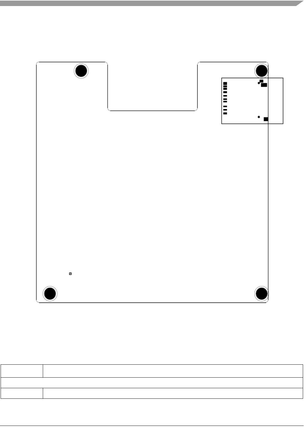
Figure 15 shows the MPC837xE-RDS board bottom view.
Figure 15. MPC837xE-RDS Bottom View
Table 2 shows references and descriptions of LEDs, jumpers, headers, and switches.
Table 2. Lists of Connectors, Jumpers, Switches, and LEDs
Reference Description
Connectors
J4 16-pin COP/JTAG connector
J11
SD Socket
MPC837xE-RDS, Rev. 1.0
22 Freescale Semiconductor
Preliminary, Subject to Change without Notice
MPC837xE-RDS Board
2.3 Connectors
This section describes the MPC837xE-RDS connectors and their pin assignments.
2.3.1 COP Connector
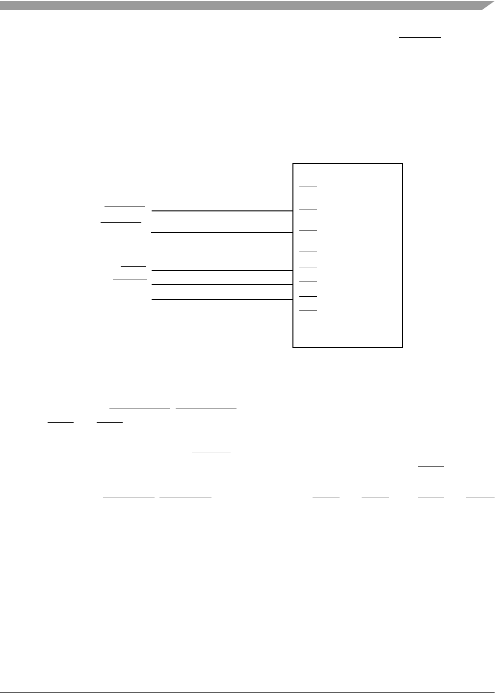
The COP connector (J4) allows the user to connect a COP/JTAG-based debugger to the MPC837xE-RDS
board for debugging. Table 3 lists the pin assignments of the COP connector.
P3, P4 32-bit 3.3 V mini PCI connector slots. The board supports up to 2 mini PCI devices.
J5 USB Type A receptacle (for USB high-speed external device)
J13 48 V DC power jack (external power adapter input)
J16 Double-eSATA port
J6 COM1 serial port terminal connector (RS-232C) for MPC837xE
P5, P6 Mini PCI-E connectors
P7 PCI-E (1X) connector
P1 RJ-45 connector Enet0 (GBit Ethernet port that connects to Ethernet Switch). Enet0 is the WAN connector and supports
PoE.
P2 RJ-45 connector Enet1 (GBit Ethernet port that connects to external device). Enet1 is the LAN connector.
J11 SD Card socket
Jumpers (Refer to Table 10 )
Switches
SW1 System reset button. Resets the MPC837xE-RDS board.
LEDs (See also Section 2.4, LEDs)
D11, D14 Controlled by the GPIO pin of MPC837xE.
D7, D8, D9 eTSEC1 Eth0 link10, link100, link1000 LEDs (top)
eTSEC2 Eth1 lind10, link100, link1000 LEDs (bottom)
D15 3.3 V Active (Power is on if lit, and 3.3 V power is good.)
Table 3. COP Connector Pin Assignments
Pin Signal Pin Signal
1 TDO 2 GND
3TDI 4TRST
5QREQ 6 VDD_SENSE
7 TCK 8 CHKSTOP_IN
Table 2. Lists of Connectors, Jumpers, Switches, and LEDs (continued)
Reference Description
MPC837xE-RDS Board
MPC837xE-RDS, Rev. 1.0
Freescale Semiconductor 23
Preliminary, Subject to Change without Notice
2.3.2 RS-232C Connectors
Serial interface COM1 is available at connector (J6) with pin assignments as shown in Table 4.
2.3.3 Serial ATA (SATA) Connector
The Double-eSATA connector (J16) connects to the serial ATA hard disks through eSATA cables.
2.3.4 Mini PCI Connector
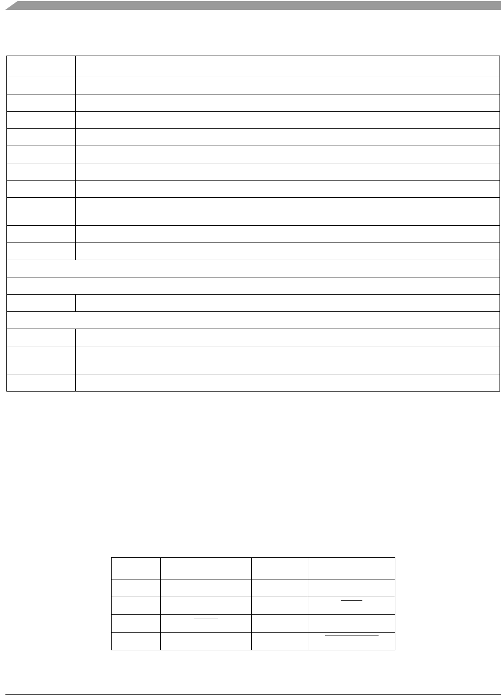
The board has two mini-PCI connectors (P3, P4) for plugging in mini PCI cards. Figure 16 shows how to
plug a mini PCI card into the board.
9TMS 10 NC
11 SRESET 12 NC
13 HRESET 14 NC
15 CHKSTOP_OUT 16 GND
Table 4. COM1 Connector Pins
Pin Signal
1 GND
2TXD
3RXD
4NC
5GND
6 GND
7CTS
8RTS
9NC
10 NC
Table 3. COP Connector Pin Assignments
Pin Signal Pin Signal
MPC837xE-RDS, Rev. 1.0
24 Freescale Semiconductor
Preliminary, Subject to Change without Notice
MPC837xE-RDS Board
Figure 16. Installation of a Mini PCI Card
2.3.5 Power Connector
J13 is a DC jack for a 48 V power supply to the MPC837xE-RDS board.
2.4 LEDs
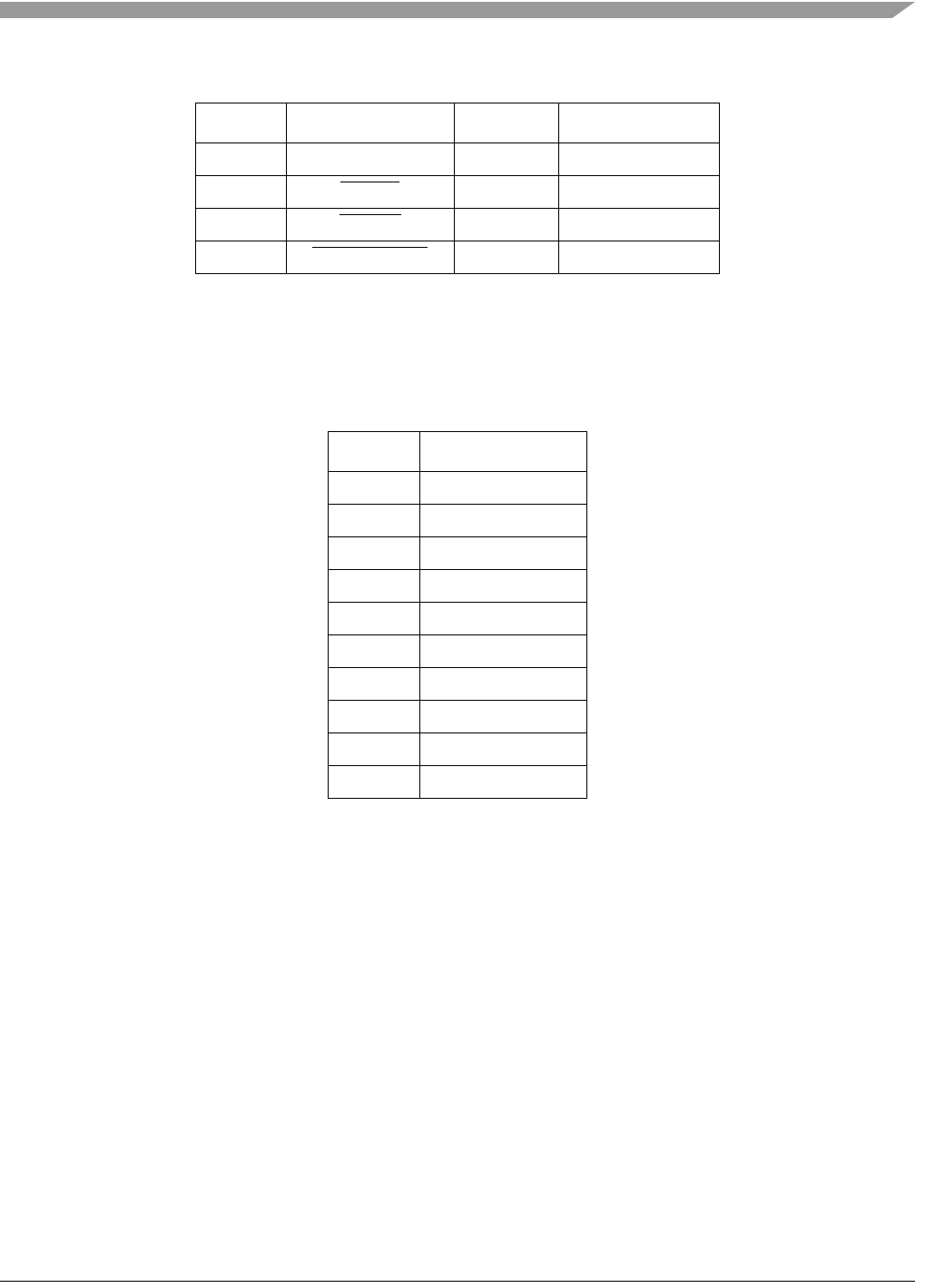
Figure 17 shows 9 LED indicators on the front panel of MPC837xE-RDS.
Figure 17. LED Indicators on the Front Panel of MPC837xE-RDS
2.4.1 Power-on LED
Green Power LED (D15): indicates the system is power-on if lit.
2.4.2 RDS Programmable LEDs
Green WiFi LED (D14): indicates whether the WiFi Card is inserted and activated (SW not implemented
yet). GPIO1[10] controls this LED. Writing 0 turns on the LED, and writing 1 turns off the LED.
Red DIAG LED (D11): indicates the status of diagnostics for MPC837xE-RDS board. The LED is flashing
when system is going through the diagnostics. It is on if the system finds some problems during the
diagnostics. And it is off if the system passes the diagnostics (SW not implemented yet). GPIO1[9]
controls this LED. Writing 0 turns on the LED, and writing 1 turns off the LED.
Mini PCI Card
1. Insert the card
2. Press downward
POWER WiFi DIAG
LAN
WAN
1000 100 10
MPC837xE-RDS Board
MPC837xE-RDS, Rev. 1.0
Freescale Semiconductor 25
Preliminary, Subject to Change without Notice
2.4.3 Ethernet LEDs
Green Link1000 LEDs (D9): indicate the link speed is 1000M on WAN and LAN. (The top LED for LAN
and the bottom one for WAN)
Green Link100 LEDs (D8): indicate the link speed is 100M on WAN and LAN. (The top LED for LAN
and the bottom one for WAN)
Green Link10 LEDs (D7): indicate the link speed is 10M on WAN and LAN. (The top LED for LAN and
the bottom one for WAN)
2.5 MPC837xE-RDS Board Configuration
This section describes the operational mode and configuration options of the MPC837xE-RDS board.
2.5.1 EEPROM
The MPC837xE-RDS board has an on-board serial EEPROM. MPC837xE acts as I2C master and it is
connected to the M24256 serial EEPROM using I2C1 as shown in Figure 18.
Figure 18. I2C EEPROM
You can use the M24256 serial EEPROM to store the reset configuration word of the MPC837xE, as well
as store the configuration registers’ values and user program if the boot sequencer of MPC837xE is
enabled.
For more details about programming the reset configuration word value in I2C EEPROM and the boot
sequencer mode, refer to the MPC8379ERM. The I2C address of the M24256 EEPROM on the bus is
0x50.
2.5.2 PCI Operating Frequency
An M66EN input pin determines the AC timing of the PCI interface. On the MPC837xE-RDS board, the
PCI agent card—connected to a mini PCI slot—determines the M66EN signal level. If a 33-MHz-only
card is inserted, the M66EN signal is driven to 0 by the PCI agent card according to the PCI specification,
or it is driven to 1 if it can perform at 66 MHz. A NOT gate inverts the signal and drives the
CFG_CLKIN_DIV input pin so the system clock continues at the same frequency.
I2C1-SCL
I2C EEROM
M24256
MPC837xE
SCL
SDA
I2C1-SDA
I2C Address = 0x50
MPC837xE-RDS, Rev. 1.0
26 Freescale Semiconductor
Preliminary, Subject to Change without Notice
MPC837xE-RDS Board
2.5.3 Reset Configuration Word
The reset configuration word (RCW) controls the clock ratios and other basic device functions, such as
PCI host or agent mode, boot location, TSEC modes, and endian mode. The reset configuration word is
divided into reset configuration word lower (RCWL) and reset configuration word higher (RCWH) and is
loaded from the local bus during the power-on or hard reset flow. The default RCW low-bit setting is
0x0404_0000. The default RCW high-bit setting is 0xA060_6C02.
The RCW is located at the lowest 64 bits of the boot Flash memory, which is 0xFC00_0000 on this board.
Figure 19 and Figure 20 show the RCW definitions.
Table 5. RCW Configuration in Flash Memory
Address
FC000000: 26262626 26262626 03030303 03030303
FC000010: 00000000 00000000 00000000 00000000
FC000020: A0A0A0A0 A0A0A0A0 60606060 60606060
FC000030: 6C6C6C6C 6C6C6C6C 02020202 02020202
0 1 2 3 4 5 6 7 8 9 10 11 12 13 14 15
Field LBIUCM DDRCM — SPMF — COREPLL
16 17 18 19 20 21 22 23 24 25 26 27 28 29 30 31
Field —
Figure 19. Reset Configuration Word Low (RCWL) Bit Settings
0 1 2 3 4 5 6 7 8 9 10 11 12 13 14 15
Field PCIHOST — PCIABR — COREDIS BMS BOOTSEQ SWEN ROMLOC RLEXT — —
16 17 18 19 20 21 22 23 24 25 26 27 28 29 30 31
Field TSEC1M TSEC2M — TLE — LDP —
Figure 20. Reset Configuration Word High (RCWH) Bit Settings
Table 6. RCWL Bit Descriptions
Bits Name Meaning Description
0 LBIUCM Local bus memory
controller clock
mode
Local Bus Controller Clock: CSB_CLK
0: Default ratio 1:1
1: ratio 2:1
1 DDRCM DDR SDRAM
memory controller
clock mode
DDR Controller Clock: CSB_CLK
0: Default ratio 1:1
1: ratio 2:1
MPC837xE-RDS Board
MPC837xE-RDS, Rev. 1.0
Freescale Semiconductor 27
Preliminary, Subject to Change without Notice
2–3 — Reserved Should be cleared.
4–7 SPMF[0–3] System PLL
multiplication factor
0000 16:1
0001 Reserved
0010 2:1
0011 3:1
0100 (default) 4:1
0101 5:1
4–7 SPMF[0–3] System PLL
multiplication factor
0110 6:1
0111 7:1
1000 8:1
1001 9:1
1010 10:1
1011 11:1
1100 12:1
1101 13:1
1110 14:1
1111 15:1
8 — Reserved Should be cleared.
9–15 COREPLL
[0–6]
Value coreclk: csb_clk VCO divider
nn 0000 n PLL bypassed PLL bypassed
00 0001 0 1:1 2
01 0001 0 1:1 4
10 0001 0 1:1 8
11 0001 0 1:1 8
00 0001 1 1.5:1 2
01 0001 1 1.5:1 4
10 0001 1 1.5:1 8
11 0001 1 1.5:1 8
00 0010 0: Default 2:1 2
Table 6. RCWL Bit Descriptions (continued)
Bits Name Meaning Description
MPC837xE-RDS, Rev. 1.0
28 Freescale Semiconductor
Preliminary, Subject to Change without Notice
MPC837xE-RDS Board
9–15 COREPLL
[0–6]
01 0010 0 2:1 4
10 0010 0 2:1 8
11 0010 0 2:1 8
00 0010 1 2.5:1 2
01 0010 1 2.5:1 4
10 0010 1 2.5:1 8
11 0010 1 2.5:1 8
00 0011 0 3:1 2
01 0011 0 3:1 4
10 0011 0 3:1 8
11 0011 0 3:1 8
16–31 — Reserved. Should be cleared.
Table 7. Reset Configuration Word High (RCWH) Bit Descriptions
Bits Name Meaning Detailed Description
0 PCIHOST PCI host mode 0 PCI agent
1: Default PCI host
1 Reserved — Should be cleared
2 PCIARB PCI arbiter 0 PCI arbiter disabled
1: Default PCI arbiter enabled
3 Reserved — Should be cleared
4 COREDIS Core disable mode 0: Default e300 enabled
1 e300 disabled
5 BMS Boot memory space 0: Default 0x0000_0000–0x007F_FFFF
1 0xFF80_0000–0xFFFF_FFFF
6–7 BOOTSEQ Boot sequencer
configuration
00: Default Boot sequencer is disabled
01 Boot sequencer load configuration from I2C
10 Boot sequencer load configuration from EEPROM
11 Reserved
8 SWEN Software watchdog
enable
0: Default Disabled
1 Enabled
Table 6. RCWL Bit Descriptions (continued)
Bits Name Meaning Description
MPC837xE-RDS Board
MPC837xE-RDS, Rev. 1.0
Freescale Semiconductor 29
Preliminary, Subject to Change without Notice
9–11 ROMLOC Boot ROM interface
location
000 DDR SDRAM
001 PCI1
010 Reserved
011 On-chip Boot ROM
100 Reserved
101 Local bus GPCM, 8 bits
110: Default Local bus GPCM, 16 bits
111 Local bus GPCM, 32 bits
12–13 RLEXT Boot ROM location
extension
00: Default Legacy mode
01 NAND Flash mode
10 Reserved
11 Reserved
14–15 Reserved — Should be cleared
16–18 TSEC1M TSEC1 Mode 000 MII
001 RMII
010 Reserved
011: Default RGMII
100 Reserved
101 RTBI
110 SGMII
110 Reserved
19–21 TSEC2M TSEC2 Mode 000 MII
001 RMII
010 Reserved
011: Default RGMII
100 Reserved
101 RTBI
110 SGMII
110 Reserved
22–27 Reserved — Should be cleared
28 TLE True little endian 0: Default Big-endian mode
1 True little endian mode
29 Reserved — Should be cleared
Table 7. Reset Configuration Word High (RCWH) Bit Descriptions (continued)
Bits Name Meaning Detailed Description
MPC837xE-RDS, Rev. 1.0
30 Freescale Semiconductor
Preliminary, Subject to Change without Notice
MPC837xE-RDS Board
2.5.4 Power Supply
The MPC837xE requires a 48 V power supply from the DC power jack or PoE for normal operation. The
48 V power supply is reduced to 5 V and 3.3 V from the DC-DC circuitry on PoE daughter board. The
1.0 V, 1.5 V, and 1.8 V are all generated from switching regulators. The 1.0 V power is for a CPU core.
The 1.5 V and 1.8 V powers are for two GE PHYs and two mini PCI-E connectors. The 1.8 V power is
also for the DDR controller.
2.5.5 Chip-Select Assignments and Memory Map
Table 8 shows an example memory map on the MPC837xE that is used for u-boot in the Flash memory.
2.6 Specifications
Table 9 lists the specifications of the MPC837xE-RDS board.
.
30 LDP LDP/CKSTP pin
mux state after reset
0 LDP[0:3] = local data parity.
1: Default LDP[0:3] = LCS[4:7]
31 Reserved — Should be cleared
Table 8. Example Memory Map, Local Access Window, and Chip-Select Assignments
Address Range Target Interface Chip-Select Line Device Name Port Size (Bits)
0x0000_0000–0x1FFF_FFFF DDR MCS0 DDR2 SDRAM (512 Mbyte) 64
0x8000_0000–0x9FFF_FFFF PCI1 Nil PCI1 memory space (512 Mbyte) 32
0xE200_0000–0xE2FF_FFFF PCI1 Nil PCI1 I/O space (16 Mbyte) 32
0xA000_0000–0xBFFF_FFFF PCI2 Nil PCI2 memory space (512 Mbyte) 32
0xE300_0000–0xE3FF_FFFF PCI2 Nil PCI2 I/O space (16 Mbyte) 32
0xE000_0000–0xEFFF_FFFF Internal bus Nil IMMR (1 Mbyte) —
0xFC00_0000–0xFFFF_FFFF Local bus LCS0 NOR Flash memory (64 Mbyte) 16
Table 9. MPC837xE-RDS Board Specifications
Characteristics Specifications
Power requirements:
(Without any plugin card and USB device)
Typical
5.0 V DC 0.009 A
3.3 V DC 1.17 A
Communication processor MPC8377E running @ up to 667 MHz
Table 7. Reset Configuration Word High (RCWH) Bit Descriptions (continued)
Bits Name Meaning Detailed Description
MPC837xE-RDS Board
MPC837xE-RDS, Rev. 1.0
Freescale Semiconductor 31
Preliminary, Subject to Change without Notice
Addressing: Total address range
Flash memory (local bus)
DDR SDRAM
4 Gbyte (32 address lines)
64 Mbyte NOR Flash
512 Mbyte DDR2 SDRAM at DDR400
Operating temperature 0oC to 70oC (room temperature)
Storage temperature –25oC to 85oC
Relative humidity 5% to 90% (noncondensing)
PCB dimensions:
Length
Width
Thickness
6693 mil
6693 mil
67 mil
Table 9. MPC837xE-RDS Board Specifications (continued)
Characteristics Specifications
MPC837xE-RDS, Rev. 1.0
32 Freescale Semiconductor
Preliminary, Subject to Change without Notice
Board Bootup
2.7 Mechanical Data
Figure 21 shows the MPC837xE-RDS dimensions (in mil). The board dimensions are 170 mm × 170 mm
(6693 mils × 6693 mils) for integration in a mini ITX chassis with a small footprint.
Figure 21. Dimensions of the MPC837xE-RDS Board
3 Board Bootup
This section describes how to boot up the MPC837xE-RDS board. The factory has preloaded a Flash
image onto the on-board Flash memory. Before powering up the board, set the on-board jumpers according
to the settings listed in Section 3.1, Board Jumper Settings.
6693.00
6693.00
2060.00 2590.00
1360.00
mounting hole
typ 4
Board Bootup
MPC837xE-RDS, Rev. 1.0
Freescale Semiconductor 33
Preliminary, Subject to Change without Notice
CAUTION
Avoid touching areas of circuitry and connectors; static discharge can
damage circuits.
3.1 Board Jumper Settings
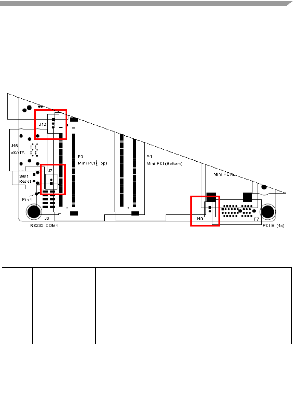
Figure 22 shows a partial top view of the MPC837xE-RDS with red outlines at jumper designators J7, J10,
and J12. A square pad indicates pin 1 of the part. Table 10 shows the default jumper settings.
Figure 22. Partial MPC837xE-RDS Top View
Table 10. Default Jumper Settings
Reference Default Jumper Setting √ = Jumper
× = No Jumper Description
J7 ×Watchdog input for MAX6829. Default is no jumper.
J10 ×12V external power input for optional connector---X1 PCI Express.
J12 2–3 √Select the reset configuration source (RST-CFG-SRC) for the MPC837xE.
Jumper 2-3 (default): 0000 Reset configuration word is loaded from
NOR Flash.
Jumper 1-2: 1111 Hard-coded option 7. Reset configuration word is
not loaded.
MPC837xE-RDS, Rev. 1.0
34 Freescale Semiconductor
Preliminary, Subject to Change without Notice
MPC837xE-RDS Software
3.2 External Connections
Figure 23shows the external connections.
Figure 23. External Connections
NOTE
Strong electromagnetic interference might disturb the normal function of
the product. If so, simply reset the product to resume normal operation by
following the steps in the software user guide. If normal function does not
return, please move the product to another location.
4 MPC837xE-RDS Software
The MPC837xE-RDS comes with a pre-installed reference design software package. This package
consists of a bootloader (u-boot), a generic PPC Linux-based system, and a suite of Wi-Fi router
applications. The software all resides in the on-board Flash memory. Upon powerup, the Linux system and
the applications run on the MPC837xE-RDS.
The MPC837xE-RDS reference software takes advantage of a tool called OpenWRT, a Linux platform for
embedded devices. Instead of trying to create a single, static firmware, OpenWrt provides a fully writable
file system with package management. This frees you from the application selection and configuration,
allowing you to customize the device through the use of packages to suit any application.
4.1 Application Features for MPC837xE-RDS reference software
The pre-installed reference design software supports the application of the Wi-Fi router, including the
following:
• 802.11 a/b/g/n
• IPv4 and IPv6
• DHCP
• DNS
•VLAN
• NAT and PAT
• Static routing
• RIP v1, v2
•VRRP
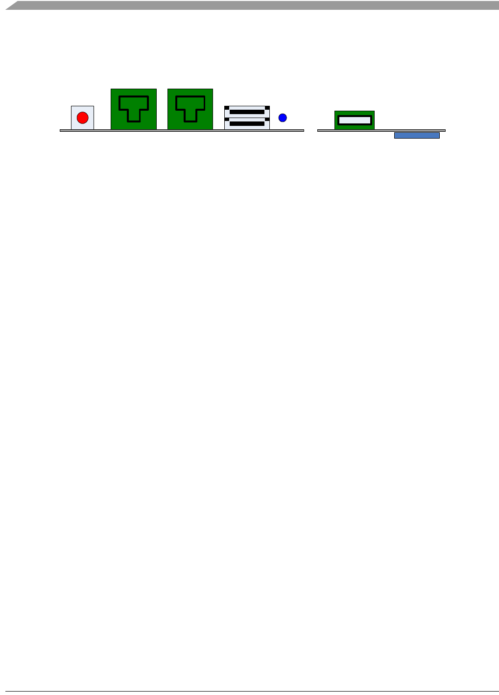
48V Power WAN
(Support PoE)
LAN eSATA Reset USB
SD Card

MPC837xE-RDS Software
MPC837xE-RDS, Rev. 1.0
Freescale Semiconductor 35
Preliminary, Subject to Change without Notice
• PPPoE
•IGMP
•UPnP
•SNMP
•QoS
Wireless Security:
• Pre-Shared Key (PSK)
• Wi-Fi Protected Access 2 (WPA2)
• 802.11i AES-CCMP
• Wired Equivalent Privacy (WEP), 128/256-bit
• 802.11i EAP authentication with RADIUS
Network Security:
• Access control
• Stateful packet inspection firewall
• Intrusion detection
• Content filtering
Virtual Private Network (VPN):
•IPSec
• PPTP
• L2TP
MPC837xE-RDS, Rev. 1.0
36 Freescale Semiconductor
Preliminary, Subject to Change without Notice
MPC837xE-RDS Software
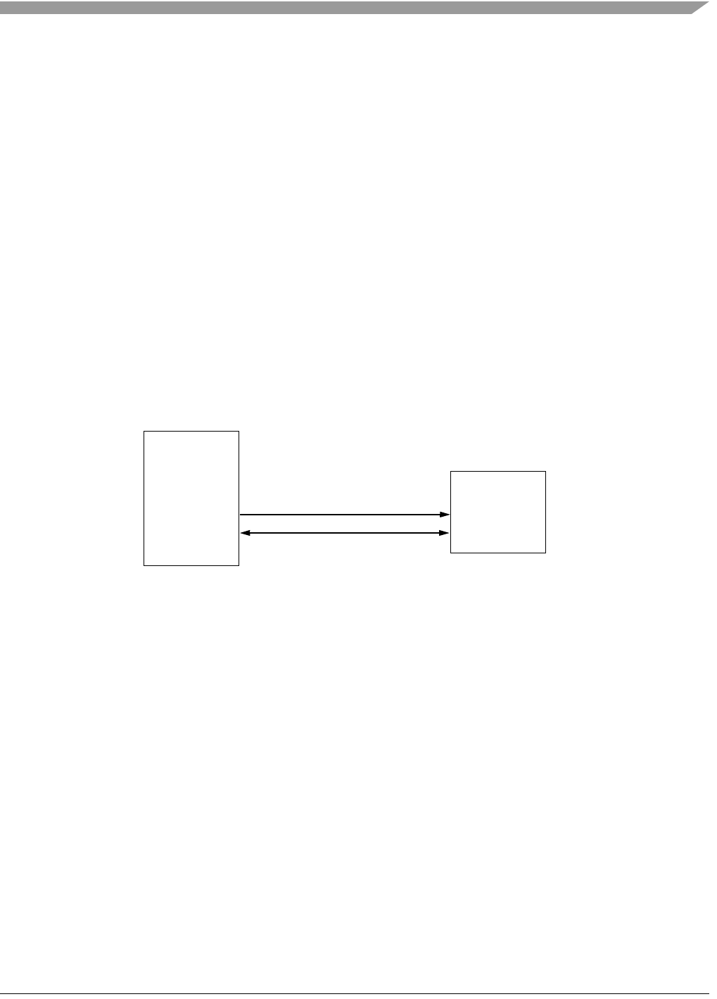
4.2 Application Connections
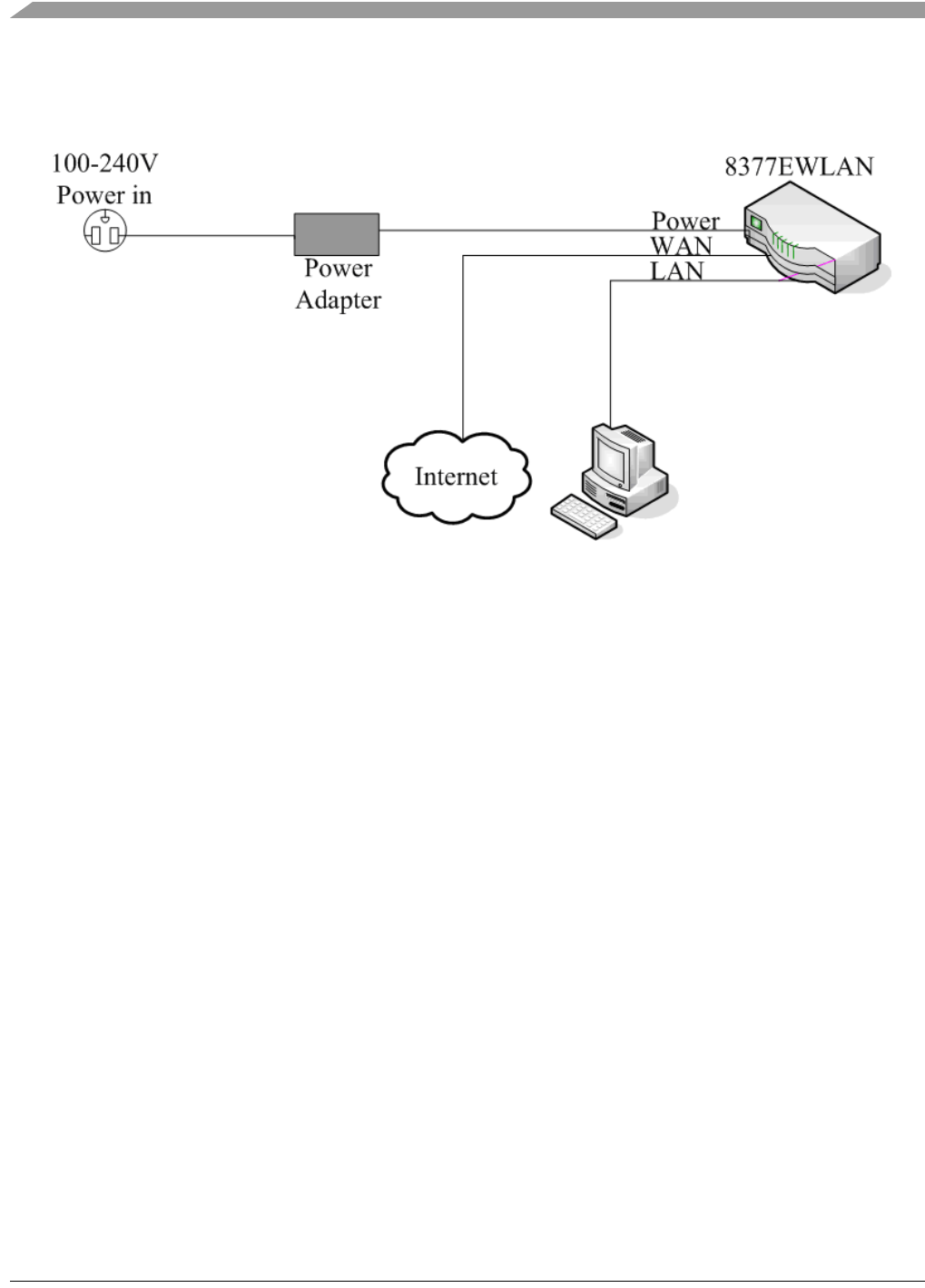
Figure 24 shows application connections for MPC837xE-RDS board.
Figure 24. MPC837xE-RDS Application Connections
Configure the MPC837xE-RDS board by using a web browser. Connect your PC to the LAN port of the
board (either directly or through a hub), then use a web browser to configure. TCP/IP settings must be
correct. The TCP/IP setting should be on the IP subnet of the MPC837xE-RDS.
• Set up the IP Address automatically:
— MPC837xE-RDS incorporates a DHCP server. The easiest method is to set your PC to get its
IP address automatically and correctly obtain the correct IP address, gateway, and DNS.
• Set up the IP Address manually:
— The default IP address of MPC837xR-RDS reference board is 192.168.1.1/24. Set the IP
address of the PC as 192.168.1.xxx/24, where xxx can be any number between 2 and 254, and
the set the default gateway to 192.168.1.1.
After setting the IP address, open a web browser and type address http://192.168.1.1. At the login window,
type admin for both User name and Password. You will then arrive at the MPC837xR-RDS main page.
After that, you can review and modify the configuration as needed. For more information, refer to the
software user guide.
Besides acting as one Wi-Fi router, MPC837xE-RDS platform can also support other utilities and
applications. For details of different applications for MPC837xE-RDS, contact your local Freescale sales
office.

Unit Assembly
MPC837xE-RDS, Rev. 1.0
Freescale Semiconductor 37
Preliminary, Subject to Change without Notice
5 Unit Assembly
The assembled unit is composed of the board assembly, an enclosure, screws, and other parts. The
instructions in this section apply if you need to assemble or reassemble the product or add peripherals
mentioned.
5.1 Assembling the Enclosure and Board Assembly
Assembling the board into the enclosure requires screwing the board onto the base, then screwing the top
and base together.
1. Place the base on a flat surface.
2. Set the board assembly in the base so the connectors and LEDs fit perfectly and the board’s
mounting holes align with the base’s mating holes.
3. With four screws and washers, screw the board to the base.
4. Align the top with the base, with the Freescale logo nearest the rear panel (connector side).
5. Screw the parts together from the bottom side of the base using four screws.
5.2 Attaching a Wi-Fi Card to the Product
Attaching the Wi-Fi card to the product requires separating the top of the enclosure from the unit, plugging
a Wi-Fi card into a mini PCI slot, installing the antenna cable into the Wi-Fi card, then reassembling the
the product.
CAUTION
Use a 3.3 V mini PCI card only. Power down before insertion or removal.
1. From the bottom of the assembled unit, remove the four screws.
2. Turn the unit right side up, plug in the Wi-Fi card, then latch it. See Figure 16 for positioning
depiction.
3. Install the antenna cable into the Wi-Fi card connector, then select the proper holes on the panel (4
on rear panel and 2 on front panel) to position the antenna.
4. Re-assemble using Steps 4 and 5 of Section 5.1, Assembling the Enclosure and Board Assembly.
5.3 Attaching a SATA hard disk to the Product
Attaching a SATA hard disk to the product requires disassembling the unit into the enclosure top and
bottom and the board assembly, inserting the hard disk, installing the cable, then re-assembling the
product.
1. Disassemble the entire unit.
2. Plug the SATA cable to J11 at the bottom side of PCBA.
3. Release the hard disk tray on the enclosure base, then position the hard disk in it.
4. Plug the other end of the SATA cable to hard disk, then position the tray in the base.
