Freescale Semiconductor MPC8377EWLAN Wireless Router User Manual MPC837xE RDS User s Guide
Freescale Semiconductor, Inc. Wireless Router MPC837xE RDS User s Guide
UserManual.wiki
>
Freescale Semiconductor
>
MPC8377EWLAN User Manual
>
hardware part
Contents
1.
hardware part
2.
software part
hardware part
Navigation menu
Upload a User Manual
Namespaces
Wiki Guide
HTML
PDF
Info
Views
User Manual
Discussion / Help
Navigation
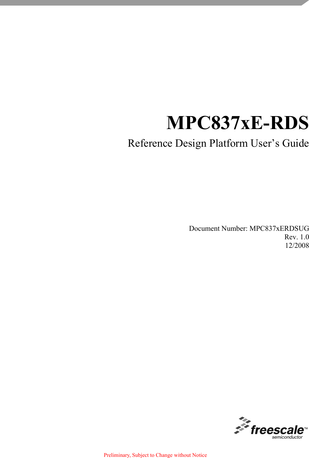
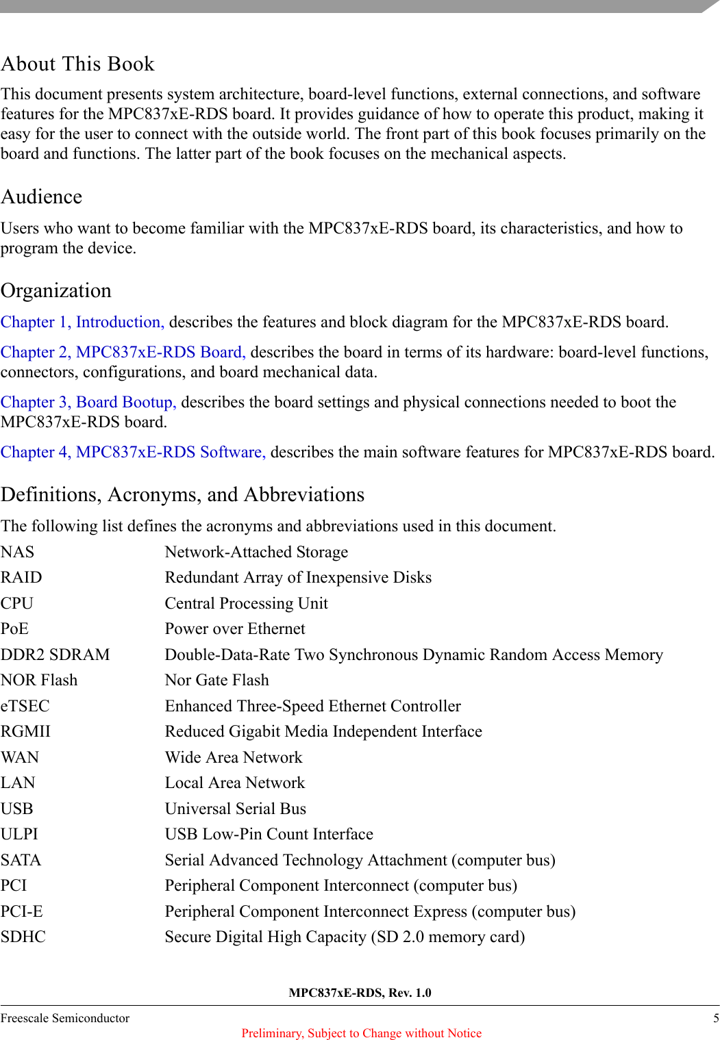
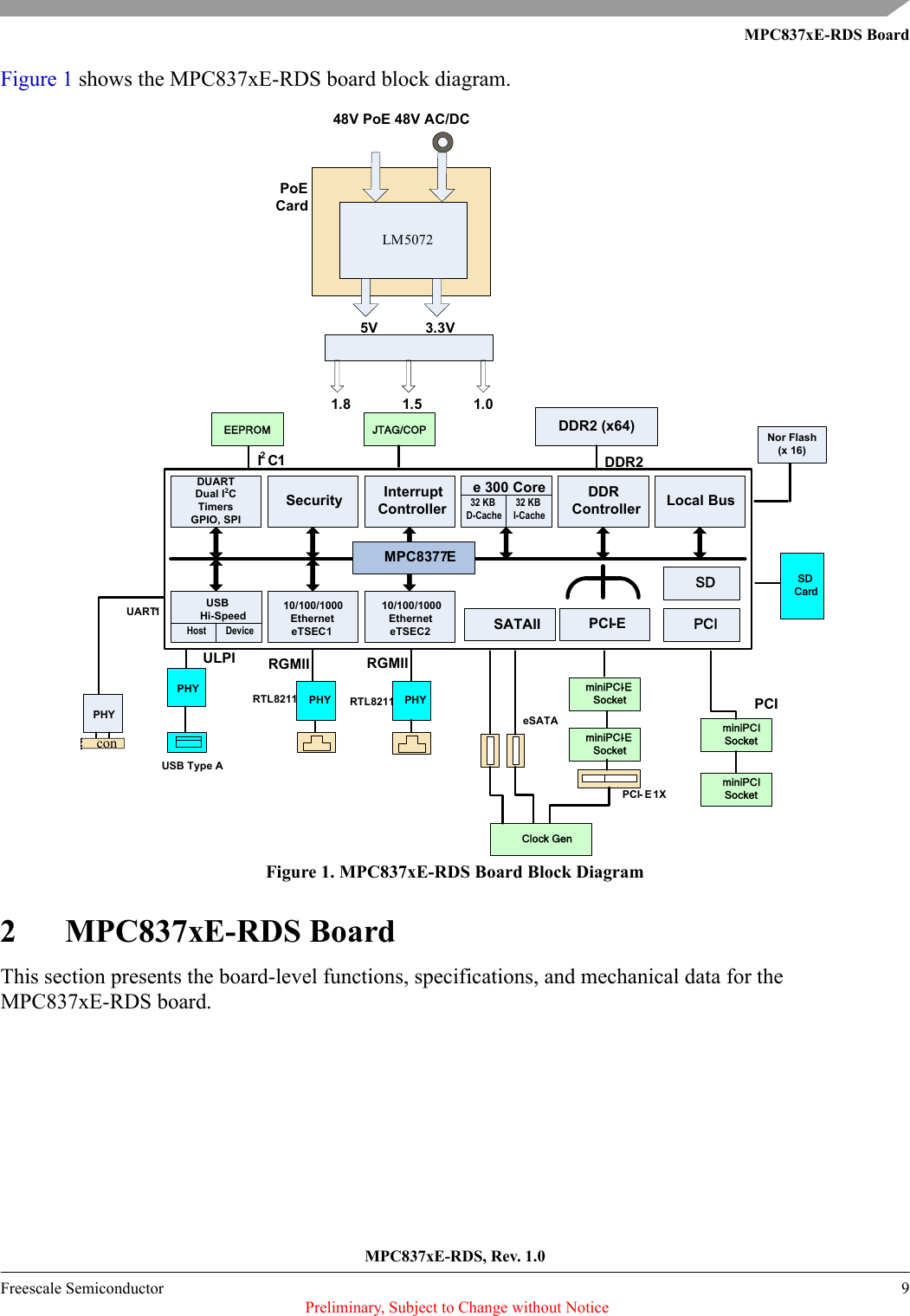
![MPC837xE-RDS, Rev. 1.014 Freescale Semiconductor Preliminary, Subject to Change without NoticeMPC837xE-RDS BoardFigure 5. DDR2 SDRAM Connection2.1.5 Local Bus ControllerThe MPC837xE local bus controller has a 32-bit LAD[0–31] address that consists of data multiplex bus and control signals. The local bus speed is up to 133 MHz. To interface with the standard memory device, an address latch must provide the address signals. The LALE is used as the latching signal. To reduce the load of the high speed 32-bit local bus interface, there is a data buffer for all low-speed devices attached to the memory controller. The local bus only drives the 64MB NOR Flash menory on the MPC837xE-RDS board:DDR2SDRAMControllerVrefGeneratorVref 0.9 V1.8 V Input VrefMSYNC_OUTMSYNC_INMPC837xEDDR2SDRAMVrefVrefDQ[0:63]DQ[32:47]DQ[0:15]DM[0:7] DM[0,1]DM[4,5]DQS[0:7] DQS[0,1]DQS[4,5]A[0:12], BA[0:2],CTRLMCK[0:3] pairsMCK0MCK2 pairDDR2SDRAMDDR2SDRAMDQ[48:63]DQ[16:31]DM[2,3]DM[6,7]DQS[2,3]DQS[6,7]MCK1 pairMCK3 pairDDR2SDRAMVrefVref1Gb(X16) 1Gb(X16)1Gb(X16) 1Gb(X16) pair](https://usermanual.wiki/Freescale-Semiconductor/MPC8377EWLAN.hardware-part/User-Guide-1098086-Page-14.png)
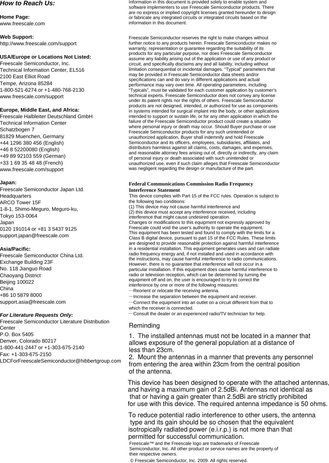
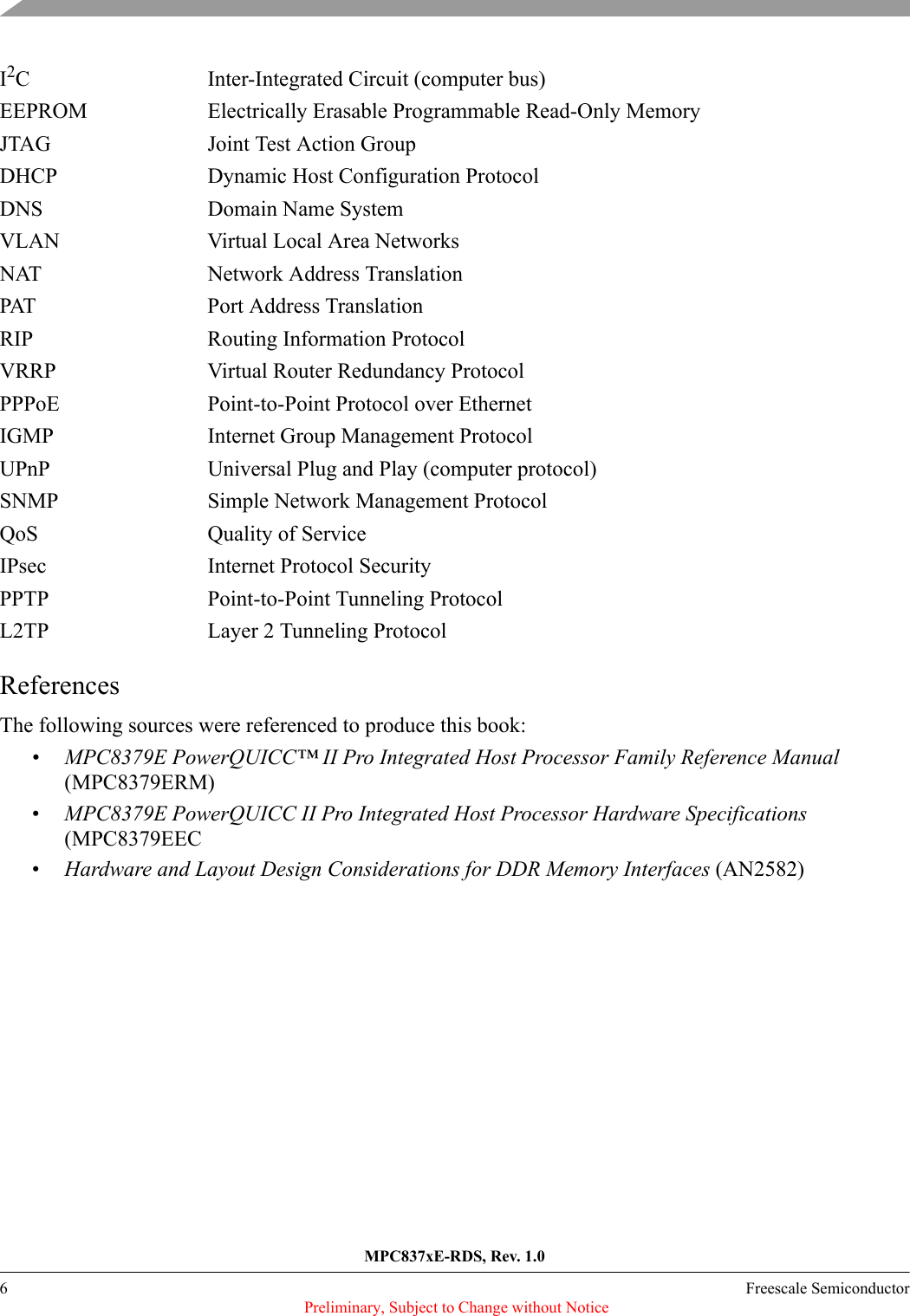
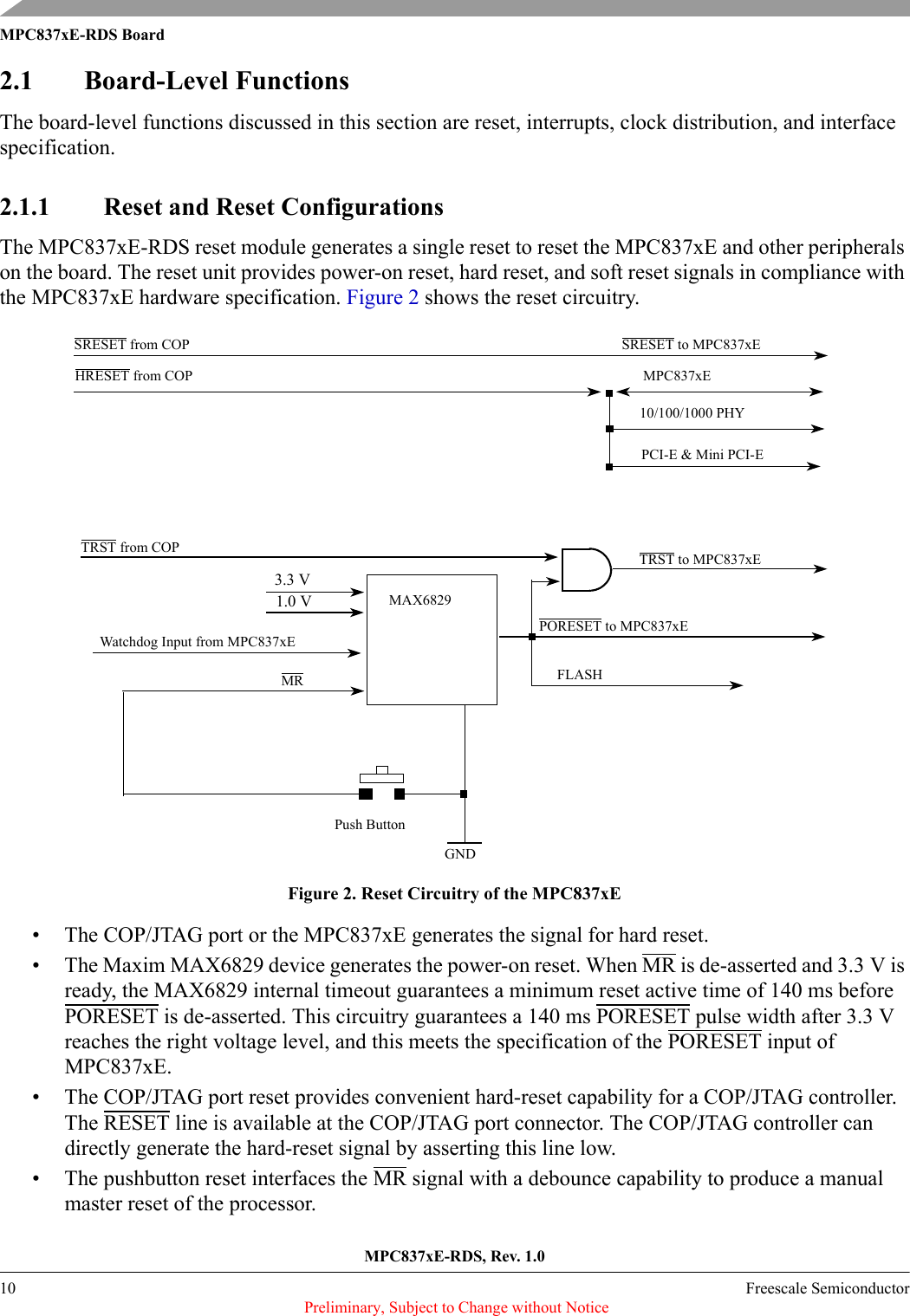
![MPC837xE-RDS BoardMPC837xE-RDS, Rev. 1.0Freescale Semiconductor 15 Preliminary, Subject to Change without NoticeFigure 6 shows the block diagram and connections for the local bus.Figure 6. Local Bus Connections2.1.6 Flash MemoryMPC837xE-RDS provides 64Mbytes NOR Flash memory using general-purpose chip-select machine (GPCM). The NOR Flash is 16-bit port size in the system. It is selected as the boot Flash when J12 pins 2 and 3 are jumpered together.2.1.7 I2CThe MPC837xE has two I2C interfaces. On the MPC837xE-RDS board, the MPC837xE serves as I2C master for both I2C buses (I2C1 and I2C2). I2C1 is connected to the following:• Serial EEPROM M24256 at address 0x50.• PCI-E and mini PCI-E socket.The M24256 serial EEPROM can store the reset configuration word of the MPC837xE, as well as store the configuration registers values if the boot sequencer of MPC837xE is enabled. The I2C address of the M24256 EEPROM on I2C1 bus is 0x50.A[24:0]CSS29GL512NNOR Flash (16-bit)MPC837xELAD[0:31]BADDR[27:30]D[15:0]LALEAddressLE Local Bus LCS0ControlOED[0:15]A[6:30]LCS0 LatchLCS0ControlLAD[6:26]LAD[0:15]Controller GNDControl SignalsLSYNC_OUTLSYNC_INLCKELCLK0LCLK1](https://usermanual.wiki/Freescale-Semiconductor/MPC8377EWLAN.hardware-part/User-Guide-1098086-Page-15.png)
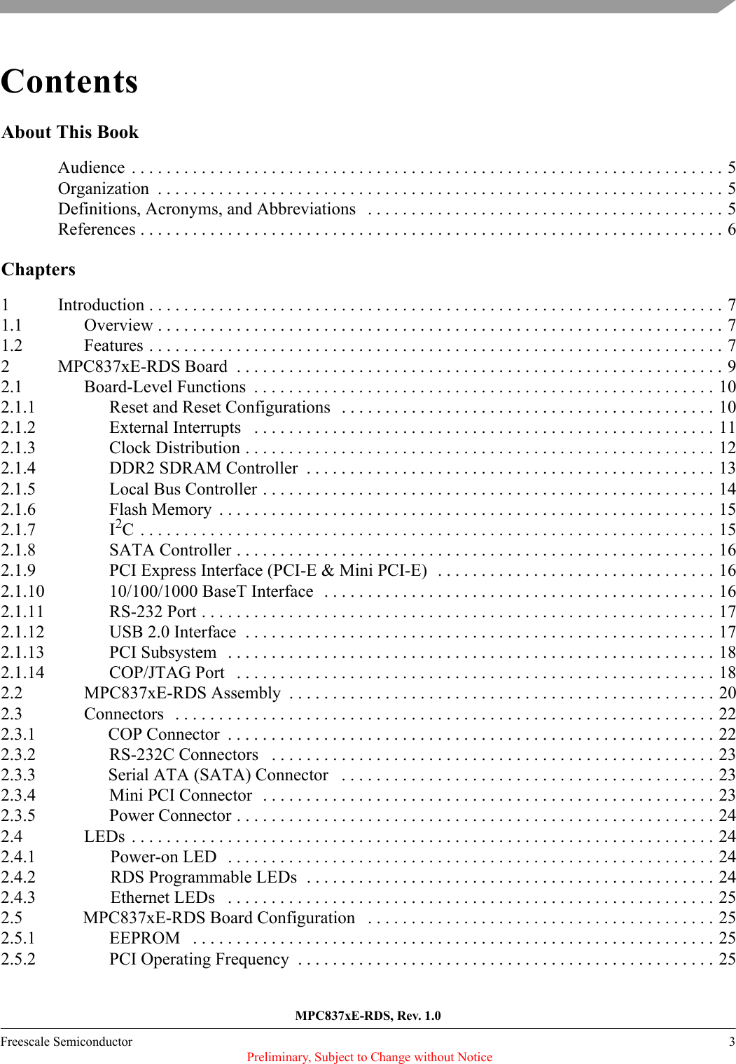
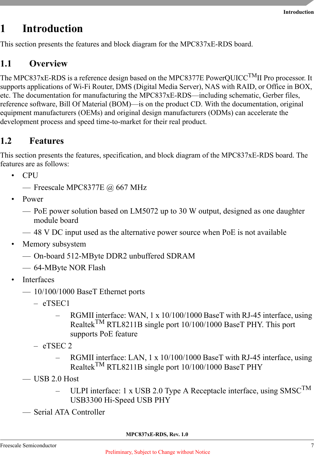
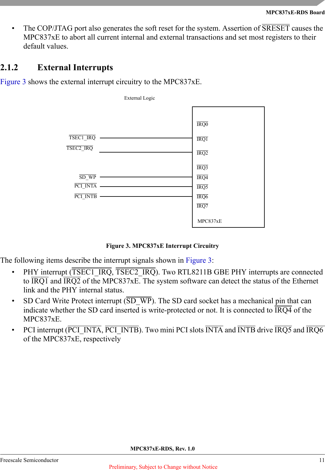
![MPC837xE-RDS, Rev. 1.018 Freescale Semiconductor Preliminary, Subject to Change without NoticeMPC837xE-RDS BoardUSB3300 PHY connects to a Type A receptacle connector that serves as a host interface. Figure 10 shows the connection of USB.Figure 10. USB Port Connections2.1.13 PCI SubsystemThe MPC837xE has PCI interfaces. It connects to two 32-bit 3.3 V mini PCI slots, as shown in Figure 11.Figure 11. PCI Subsystem2.1.14 COP/JTAG PortThe common on-chip processor (COP) is part of the MPC837xE JTAG module and is implemented as a set of additional instructions and logic. This port can connect to a dedicated emulator for extensive system debugging. Several third-party emulators in the market can connect to the host computer through the MPC837xEULPI_D[7:0]ULPI_STPULPI_NXTULPI_CLKDIRUSB3300D[7:0]STPNXTCLKOUTULPI_DIR VBUSDMID5VDPUSB_TYPE_A_RECEPTACLEMPC837xE32-Bit PCIPCI-AD[0:31]PCI-CBE[0:3]PCI-REQ0 PCI-GNT0 PCI-CTRL 32-Bit 3.3 VMini PCI Slot32-Bit 3.3 VMini PCI SlotPCI-REQ1PCI-GNT1AD15AD14](https://usermanual.wiki/Freescale-Semiconductor/MPC8377EWLAN.hardware-part/User-Guide-1098086-Page-18.png)
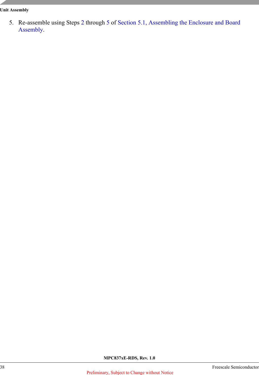
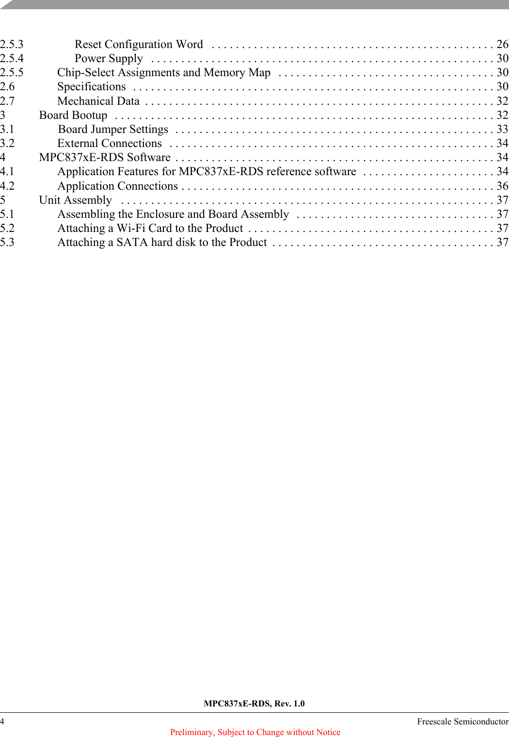
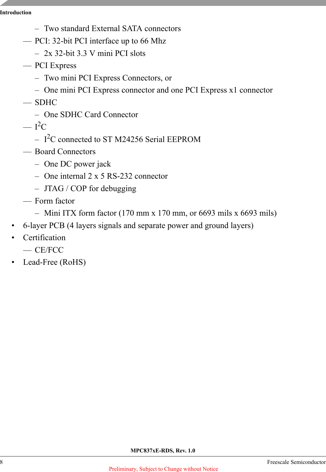
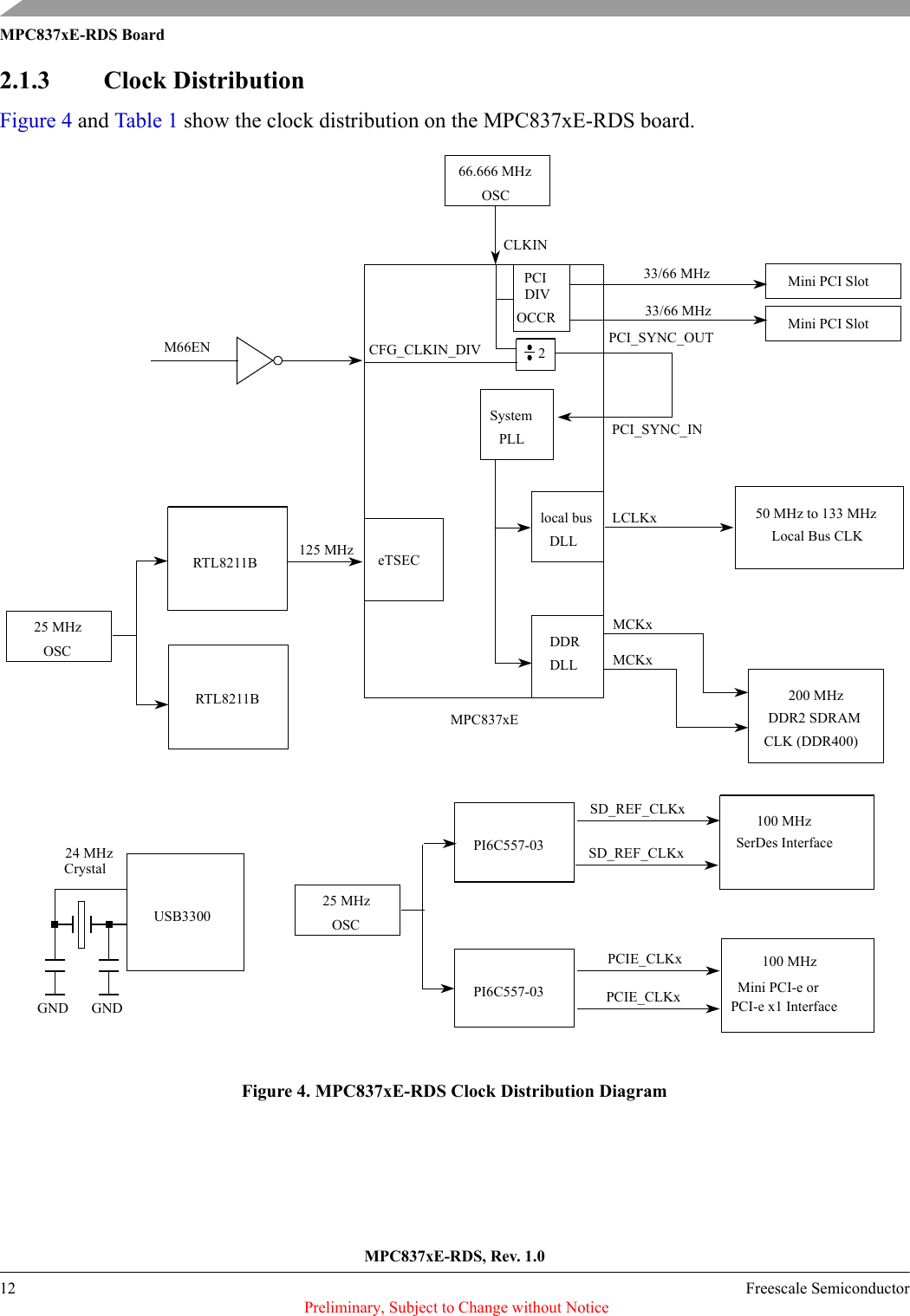
![MPC837xE-RDS, Rev. 1.024 Freescale Semiconductor Preliminary, Subject to Change without NoticeMPC837xE-RDS BoardFigure 16. Installation of a Mini PCI Card2.3.5 Power ConnectorJ13 is a DC jack for a 48 V power supply to the MPC837xE-RDS board.2.4 LEDsFigure 17 shows 9 LED indicators on the front panel of MPC837xE-RDS.Figure 17. LED Indicators on the Front Panel of MPC837xE-RDS2.4.1 Power-on LEDGreen Power LED (D15): indicates the system is power-on if lit.2.4.2 RDS Programmable LEDsGreen WiFi LED (D14): indicates whether the WiFi Card is inserted and activated (SW not implemented yet). GPIO1[10] controls this LED. Writing 0 turns on the LED, and writing 1 turns off the LED.Red DIAG LED (D11): indicates the status of diagnostics for MPC837xE-RDS board. The LED is flashing when system is going through the diagnostics. It is on if the system finds some problems during the diagnostics. And it is off if the system passes the diagnostics (SW not implemented yet). GPIO1[9] controls this LED. Writing 0 turns on the LED, and writing 1 turns off the LED.Mini PCI Card1. Insert the card2. Press downwardPOWER WiFi DIAGLANWAN1000 100 10](https://usermanual.wiki/Freescale-Semiconductor/MPC8377EWLAN.hardware-part/User-Guide-1098086-Page-24.png)
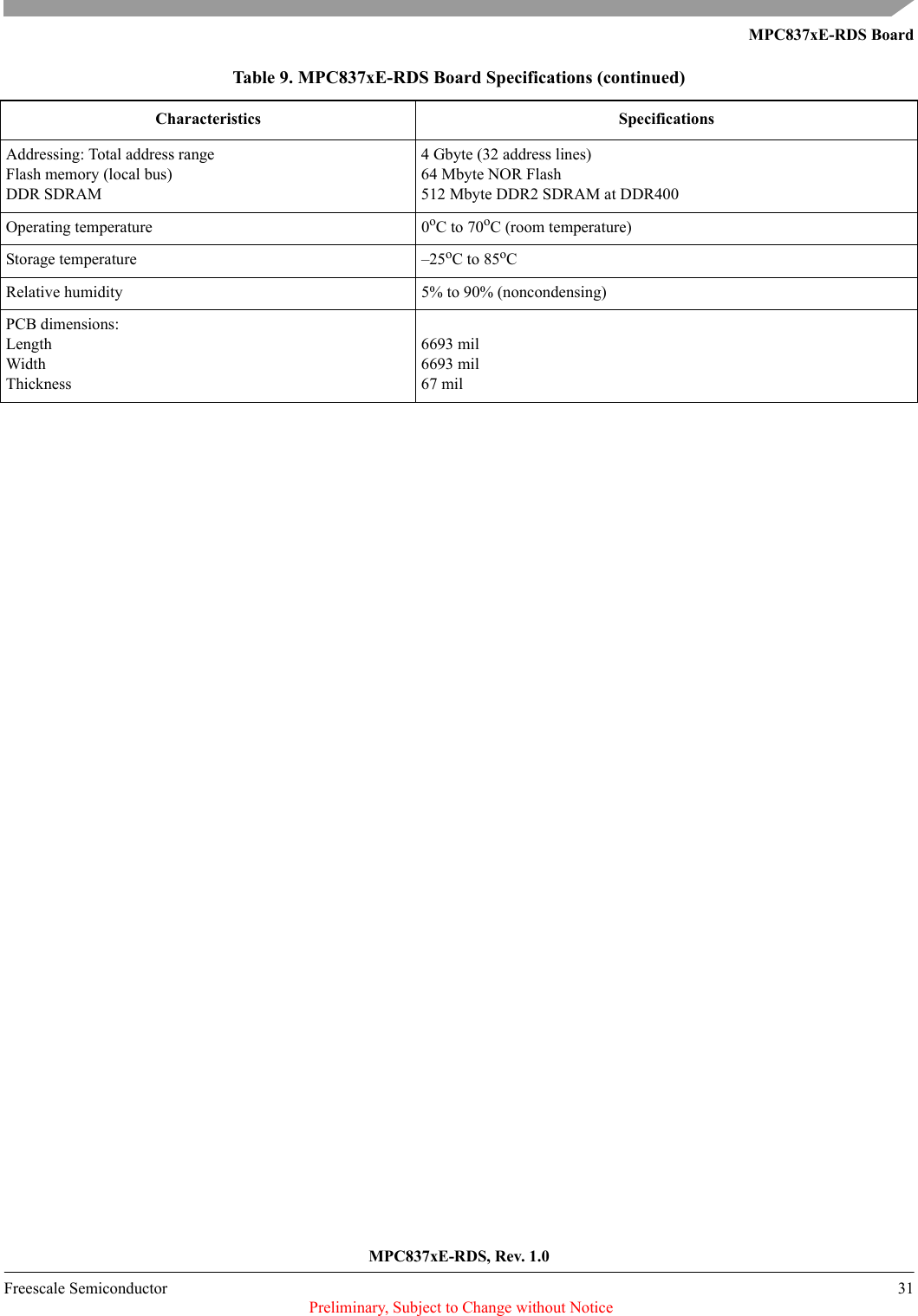
![MPC837xE-RDS BoardMPC837xE-RDS, Rev. 1.0Freescale Semiconductor 27 Preliminary, Subject to Change without Notice2–3 — Reserved Should be cleared.4–7 SPMF[0–3] System PLL multiplication factor0000 16:10001 Reserved0010 2:10011 3:10100 (default) 4:10101 5:14–7 SPMF[0–3] System PLL multiplication factor0110 6:10111 7:11000 8:11001 9:11010 10:11011 11:11100 12:11101 13:11110 14:11111 15:18 — Reserved Should be cleared.9–15 COREPLL[0–6]Value coreclk: csb_clk VCO dividernn 0000 n PLL bypassed PLL bypassed00 0001 0 1:1 201 0001 0 1:1 410 0001 0 1:1 811 0001 0 1:1 800 0001 1 1.5:1 201 0001 1 1.5:1 410 0001 1 1.5:1 811 0001 1 1.5:1 800 0010 0: Default 2:1 2Table 6. RCWL Bit Descriptions (continued)Bits Name Meaning Description](https://usermanual.wiki/Freescale-Semiconductor/MPC8377EWLAN.hardware-part/User-Guide-1098086-Page-27.png)
![MPC837xE-RDS, Rev. 1.028 Freescale Semiconductor Preliminary, Subject to Change without NoticeMPC837xE-RDS Board9–15 COREPLL[0–6]01 0010 0 2:1 410 0010 0 2:1 811 0010 0 2:1 800 0010 1 2.5:1 201 0010 1 2.5:1 410 0010 1 2.5:1 811 0010 1 2.5:1 800 0011 0 3:1 201 0011 0 3:1 410 0011 0 3:1 811 0011 0 3:1 816–31 — Reserved. Should be cleared.Table 7. Reset Configuration Word High (RCWH) Bit DescriptionsBits Name Meaning Detailed Description0 PCIHOST PCI host mode 0 PCI agent1: Default PCI host1 Reserved — Should be cleared2 PCIARB PCI arbiter 0 PCI arbiter disabled1: Default PCI arbiter enabled3 Reserved — Should be cleared4 COREDIS Core disable mode 0: Default e300 enabled1 e300 disabled5 BMS Boot memory space 0: Default 0x0000_0000–0x007F_FFFF1 0xFF80_0000–0xFFFF_FFFF6–7 BOOTSEQ Boot sequencer configuration00: Default Boot sequencer is disabled01 Boot sequencer load configuration from I2C10 Boot sequencer load configuration from EEPROM11 Reserved8 SWEN Software watchdog enable0: Default Disabled1 EnabledTable 6. RCWL Bit Descriptions (continued)Bits Name Meaning Description](https://usermanual.wiki/Freescale-Semiconductor/MPC8377EWLAN.hardware-part/User-Guide-1098086-Page-28.png)
![MPC837xE-RDS, Rev. 1.030 Freescale Semiconductor Preliminary, Subject to Change without NoticeMPC837xE-RDS Board2.5.4 Power SupplyThe MPC837xE requires a 48 V power supply from the DC power jack or PoE for normal operation. The 48 V power supply is reduced to 5 V and 3.3 V from the DC-DC circuitry on PoE daughter board. The 1.0 V, 1.5 V, and 1.8 V are all generated from switching regulators. The 1.0 V power is for a CPU core. The 1.5 V and 1.8 V powers are for two GE PHYs and two mini PCI-E connectors. The 1.8 V power is also for the DDR controller.2.5.5 Chip-Select Assignments and Memory MapTable 8 shows an example memory map on the MPC837xE that is used for u-boot in the Flash memory.2.6 SpecificationsTable 9 lists the specifications of the MPC837xE-RDS board..30 LDP LDP/CKSTP pin mux state after reset0 LDP[0:3] = local data parity.1: Default LDP[0:3] = LCS[4:7]31 Reserved — Should be clearedTable 8. Example Memory Map, Local Access Window, and Chip-Select AssignmentsAddress Range Target Interface Chip-Select Line Device Name Port Size (Bits)0x0000_0000–0x1FFF_FFFF DDR MCS0 DDR2 SDRAM (512 Mbyte) 640x8000_0000–0x9FFF_FFFF PCI1 Nil PCI1 memory space (512 Mbyte) 320xE200_0000–0xE2FF_FFFF PCI1 Nil PCI1 I/O space (16 Mbyte) 320xA000_0000–0xBFFF_FFFF PCI2 Nil PCI2 memory space (512 Mbyte) 320xE300_0000–0xE3FF_FFFF PCI2 Nil PCI2 I/O space (16 Mbyte) 320xE000_0000–0xEFFF_FFFF Internal bus Nil IMMR (1 Mbyte) —0xFC00_0000–0xFFFF_FFFF Local bus LCS0 NOR Flash memory (64 Mbyte) 16Table 9. MPC837xE-RDS Board SpecificationsCharacteristics SpecificationsPower requirements: (Without any plugin card and USB device) Typical 5.0 V DC 0.009 A3.3 V DC 1.17 ACommunication processor MPC8377E running @ up to 667 MHzTable 7. Reset Configuration Word High (RCWH) Bit Descriptions (continued)Bits Name Meaning Detailed Description](https://usermanual.wiki/Freescale-Semiconductor/MPC8377EWLAN.hardware-part/User-Guide-1098086-Page-30.png)