Freescale Semiconductor USBKW24D USB Dongle User Manual MKW22D512V good
Freescale Semiconductor, Inc. USB Dongle MKW22D512V good
UserManual.wiki
>
Freescale Semiconductor
>
USBKW24D User Manual
>
Manual
Contents
1.
Manual
2.
Quick Start Guide
3.
Reference Manual
Manual
Navigation menu
Upload a User Manual
Namespaces
Wiki Guide
HTML
PDF
Info
Views
User Manual
Discussion / Help
Navigation
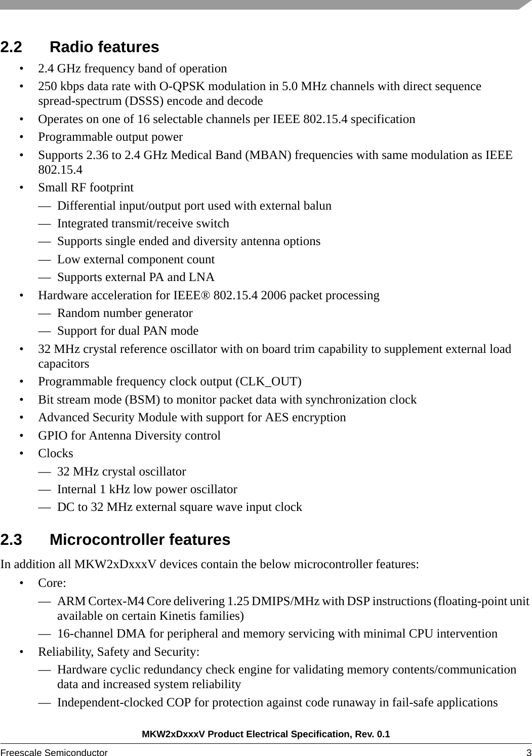
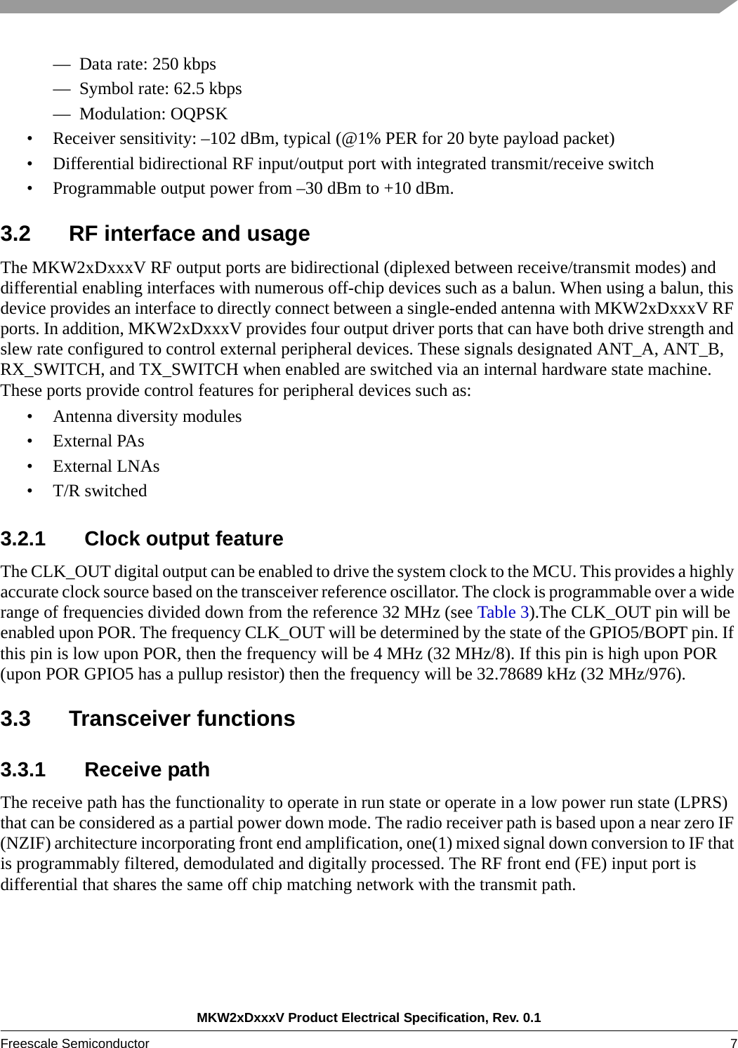
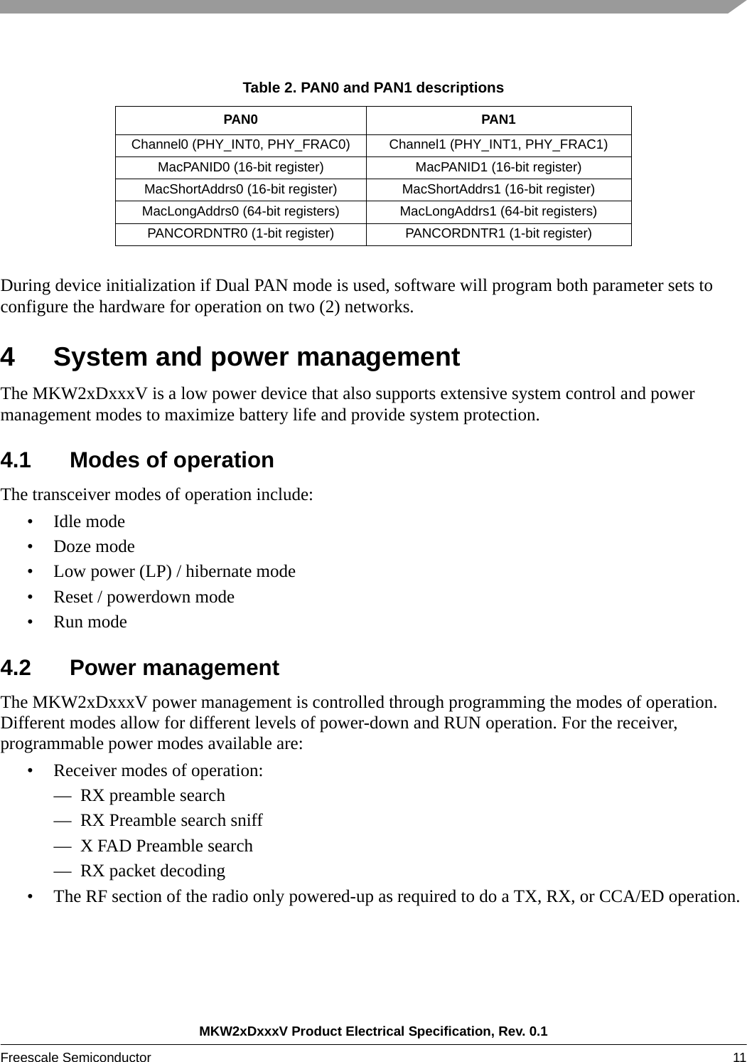
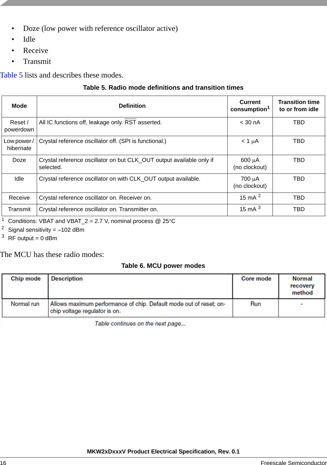
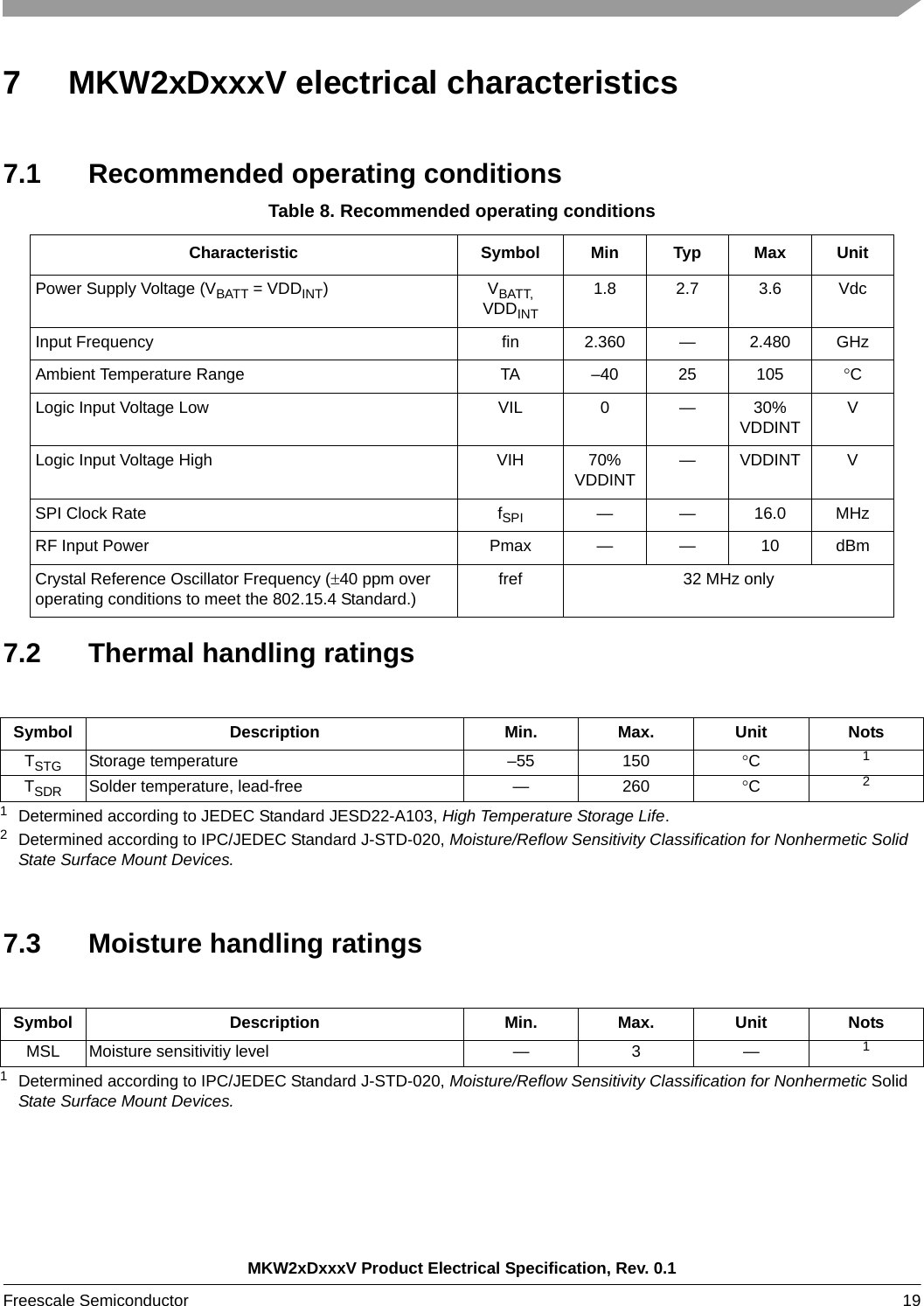
![MKW2xDxxxV Product Electrical Specification, Rev. 0.112 Freescale Semiconductor 5 Radio PeripheralsThe MKW2xDxxxV provides a set of I/O pins useful for suppling a system clock to the MCU, controlling external RF modules/circuitry, and GPIO. In addition, there is a special option for streaming the digital packet data for external monitoring (BSM).5.1 Clock output (CLK_OUT)MKW2xDxxxV integrates a programmable clock to source numerous frequencies for connection with various MCUs. Package pin 39 can be used to provide this clock source as required allowing the user to make adjustments per their application requirement. The transceiver CLK_OUT pin is internally connected to the MCU EXTAL pin so that no external connection is needed to drive the MCU clock.Care must be taken that the clock output signal does not “talk” or interfere with the reference oscillator or the radio. Additional functionality this feature supports is:• 3 clock domains (XTAL, SCLK, SDM_CK).• Built in synchronization at all clock domain crossings.• Aggressive clock gating in the XTAL domain to minimize dynamic current consumption based on the power mode selected.• XTAL domain can be completely gated off (hibernate mode) • SPI communication allowed in hibernate• Single-clock domain in scan modeTable 3. CLK_OUT tableThere is an enable and disable bit for CLK_OUT. When disabling, the clock output will optionally continue to run for 128 clock cycles after disablement. There will also be one (1) bit available to adjust the CLK_OUT I/O pad drive strength. 5.2 Bit streaming mode (BSM)Another peripheral option is bit streaming mode that when activated allows all 802.15.4 packet data, received or transmitted, to be serialized and shifted out to external hardware for further processing. A simple development system can be crafted to consume the BSM outputs and generate packet trace data for CLK_OUT_DIV [2:0] CLK_OUT frequency Comments032 MHz116 MHz28 MHz3 4 MHz DEFAULT if GPIO5/BOPT=042 MHz51 MHz6 62.5 kHz7 32.786 kHz DEFAULT if GPIO5/BOPT=1](https://usermanual.wiki/Freescale-Semiconductor/USBKW24D.Manual/User-Guide-2333153-Page-12.png)
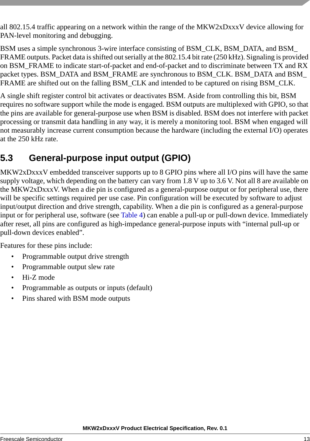
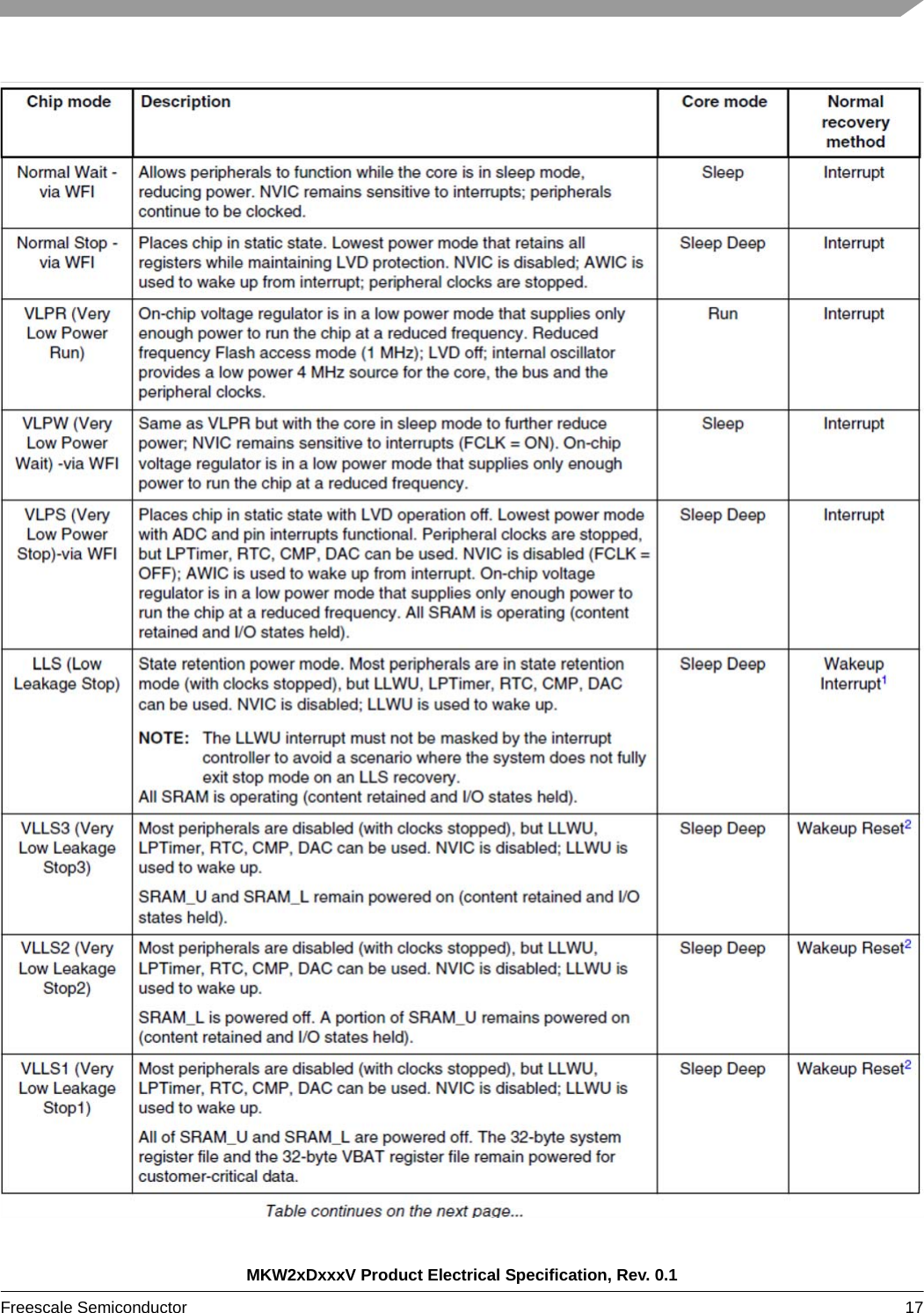
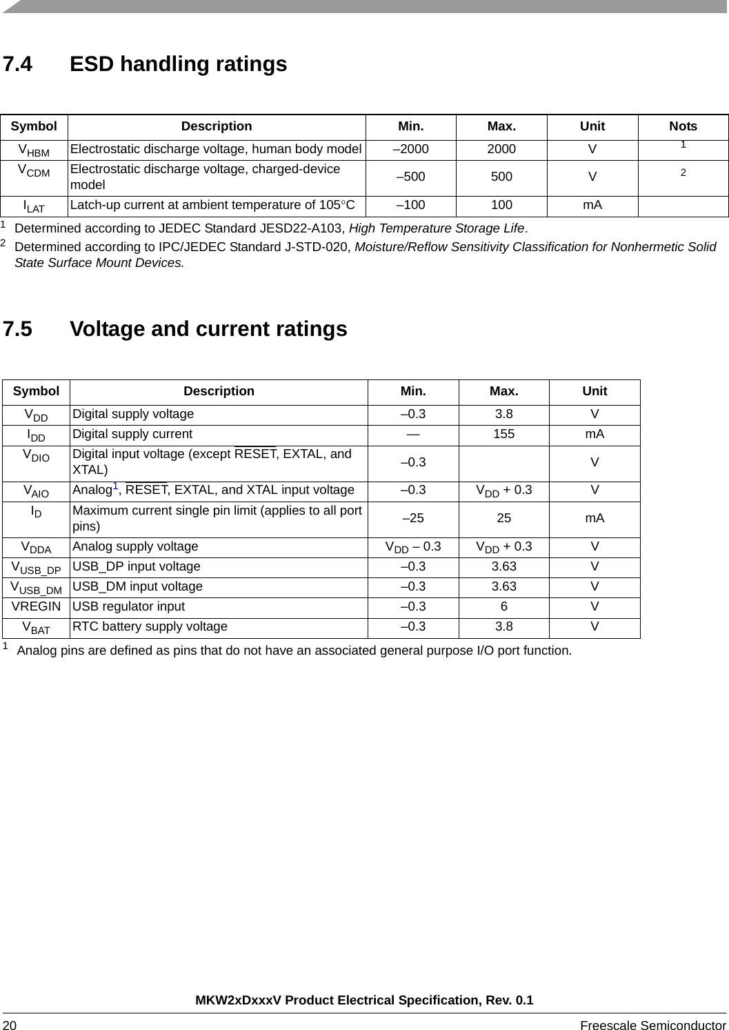
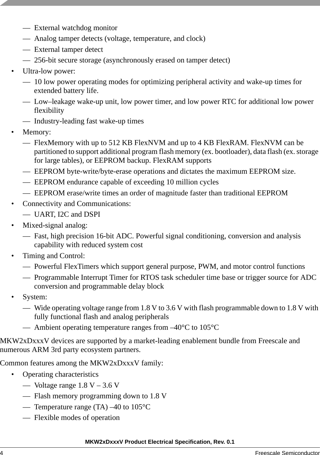
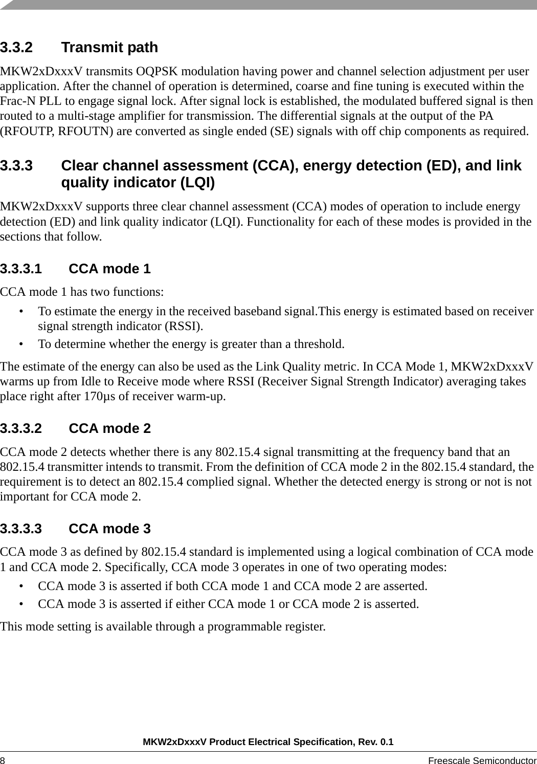
![MKW2xDxxxV Product Electrical Specification, Rev. 0.1Freescale Semiconductor 23 8.2 General8.2.1 AC electrical characteristicsUnless otherwise specified, propagation delays are measured from the 50% to the 50% point, and rise and fall times are measured at the 20% and 80% points, as shown in the following figure.Figure 2. Input signal measurement referenceAll digital I/O switching characteristics assume:• output pins—have CL=30pF loads,—are configured for fast slew rate (PORTx_PCRn[SRE]=0), and—are configured for high drive strength (PORTx_PCRn[DSE]=1)• input pins— have their passive filter disabled (PORTx_PCRn[PFE]=0)](https://usermanual.wiki/Freescale-Semiconductor/USBKW24D.Manual/User-Guide-2333153-Page-23.png)
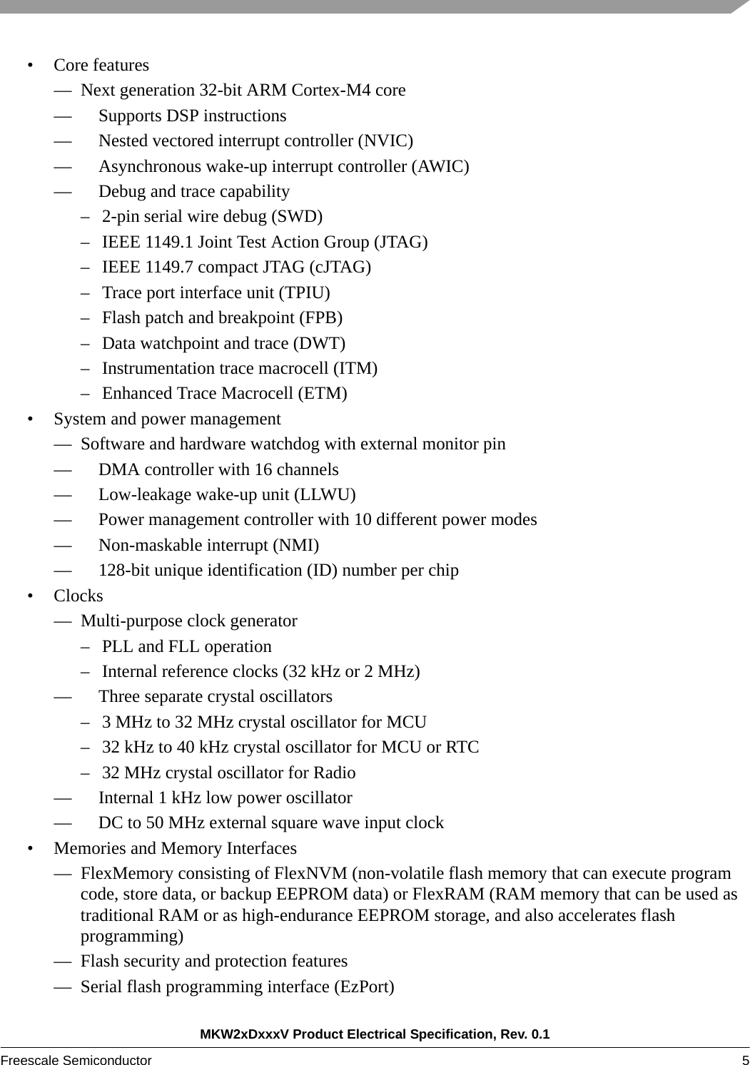
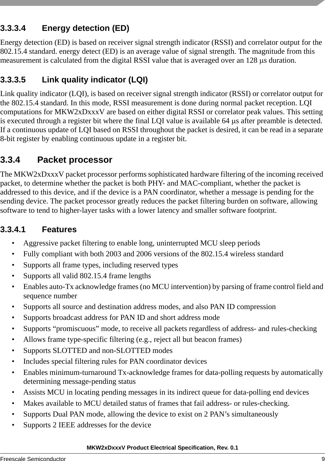
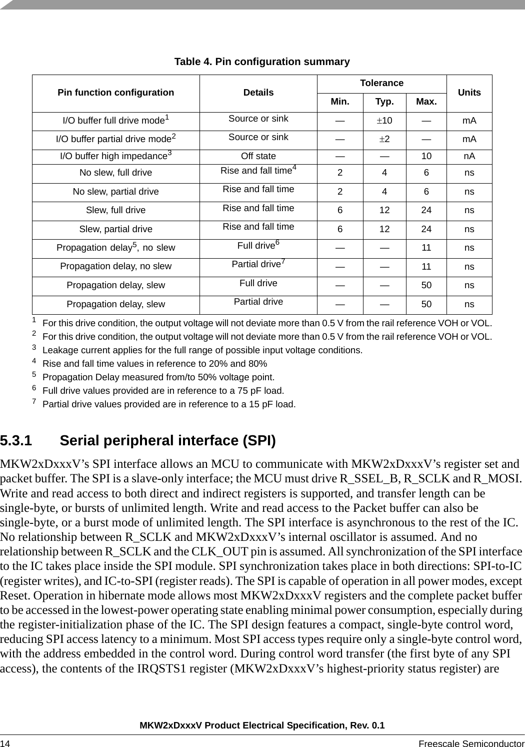
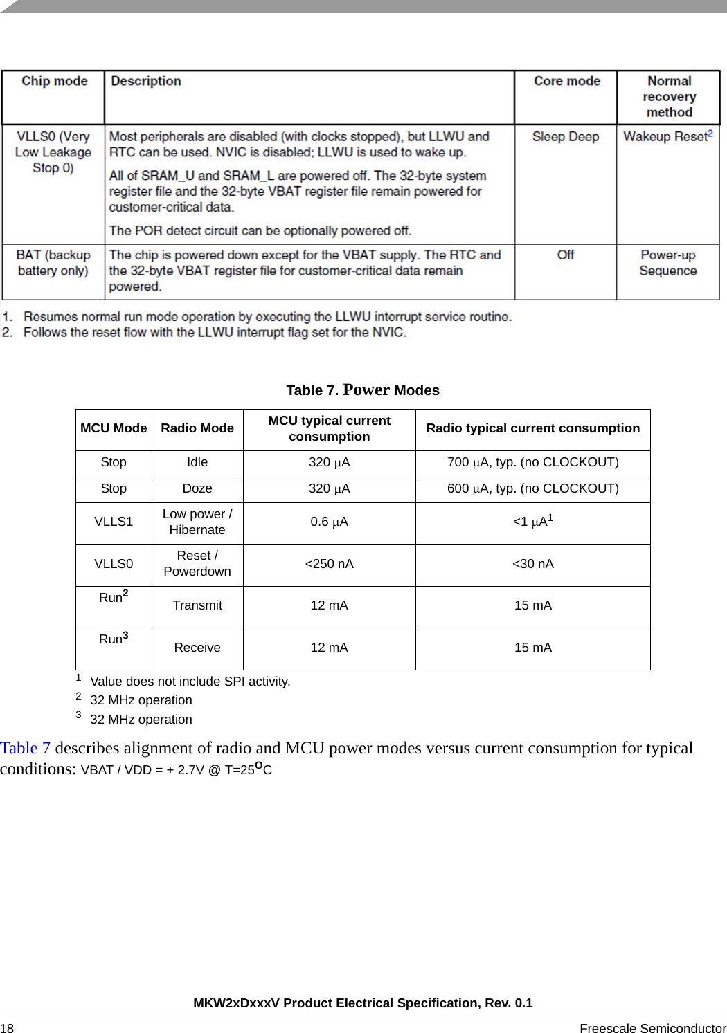
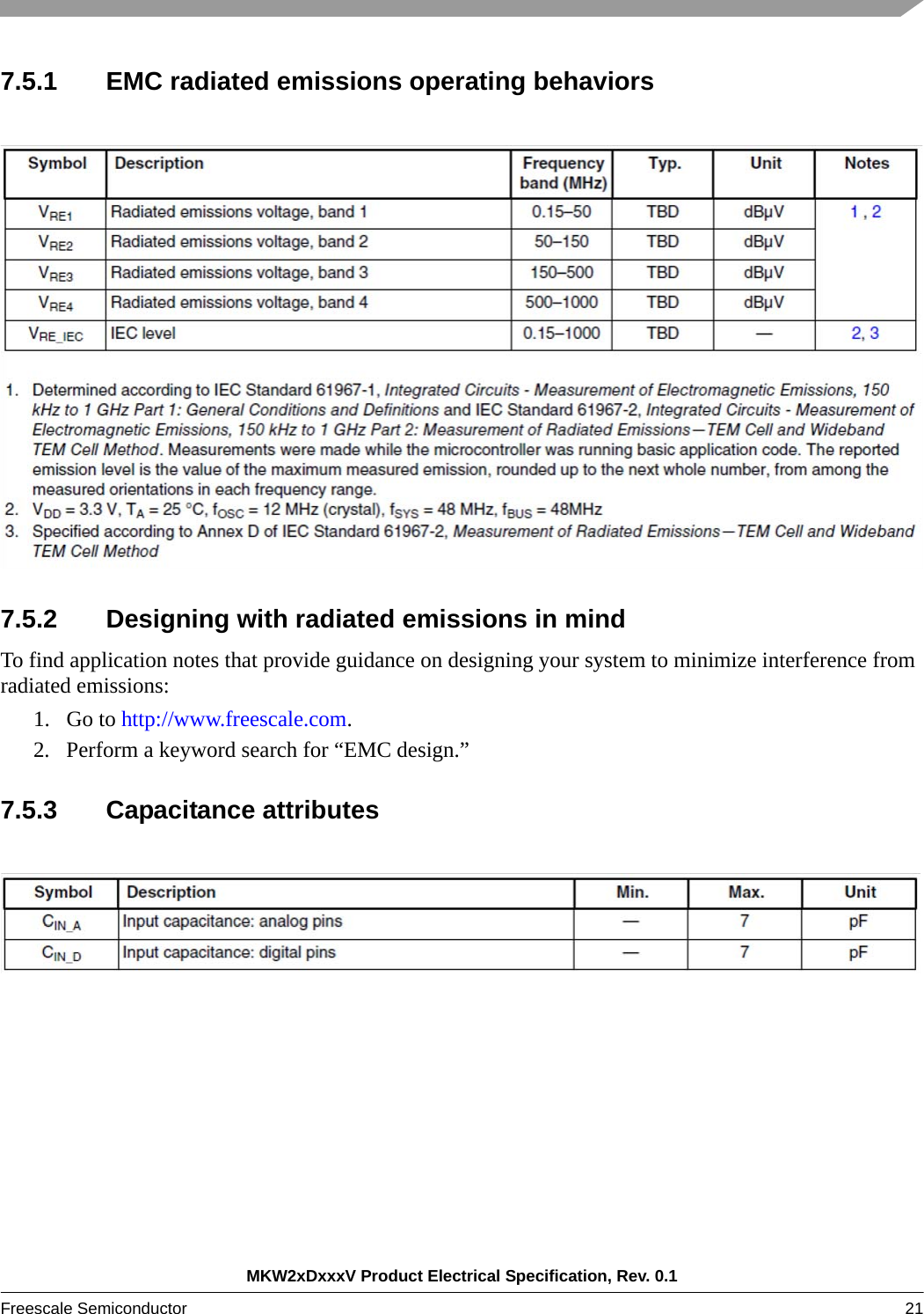
![MKW2xDxxxV Product Electrical Specification, Rev. 0.168 Freescale Semiconductor 9.2 AC electrical characteristicsTable 11. Receiver AC electrical characteristics (VBATT, VDDINT=2.7 V, TA=25 °C, fref=32 MHz, unless otherwise noted)Characteristic Symbol Min Typ Max UnitSensitivity for 1% packet error rate (PER) (–40 to +105 °C) SENSper — –99 –97 dBmSensitivity for 1% packet error rate (PER) (+25 °C) SENSper — –102 dBmSaturation (maximum input level) SENSmax — +10 — dBmChannel rejection for dual port mode (1% PER and desired signal –82 dBm)+5 MHz (adjacent channel)–5 MHz (adjacent channel)+10 MHz (alternate channel)–10 MHz (alternate channel)>= 15 MHz—————3834474755—————dBdBdBdBdBFrequency error tolerance — — 200 kHzSymbol rate error tolerance 80 — — ppmTable 12. Transmitter AC electrical characteristics(VBATT, VDDINT=2.7 V, TA=25°C, fref=32 MHz, unless otherwise noted)Characteristic Symbol Min Typ Max UnitPower spectral density1, absolute limit from –40C to +105C1[f-fc] > 3.5 MHz, average spectral power is measured in 100 kHz resolution BW. –30 — — dBmPower Spectral Density2, Relative limit from –40C to +105C2For the relative limit, the reference level is the highest reference power measured within 1 MHz of the carrier frequency–20 — — dBNominal output power Pout –0.5 0 0.5 dBmMaximum output power — 10 — dBmError vector magnitude EVM — 8 13 %Output power control range33Measurement is at the package pin on the output of the Tx/Rx switch. It does not degrade more than 2 dB across temperature and an additional 1 dB across all processes. Power adjustment will span nominally from –30 dBm to +10 dBm in 21 steps @ 2 dBm / step. —40—dBOver the air data rate — 250 — kbps2nd harmonic44Measured with output power set to nominal (0 dBm) and temperature @ 25°C. If trap filter is needed must meet reference board size requirements.—<-50<-40dBm3rd harmonic 4—<-50<-40dBm](https://usermanual.wiki/Freescale-Semiconductor/USBKW24D.Manual/User-Guide-2333153-Page-68.png)