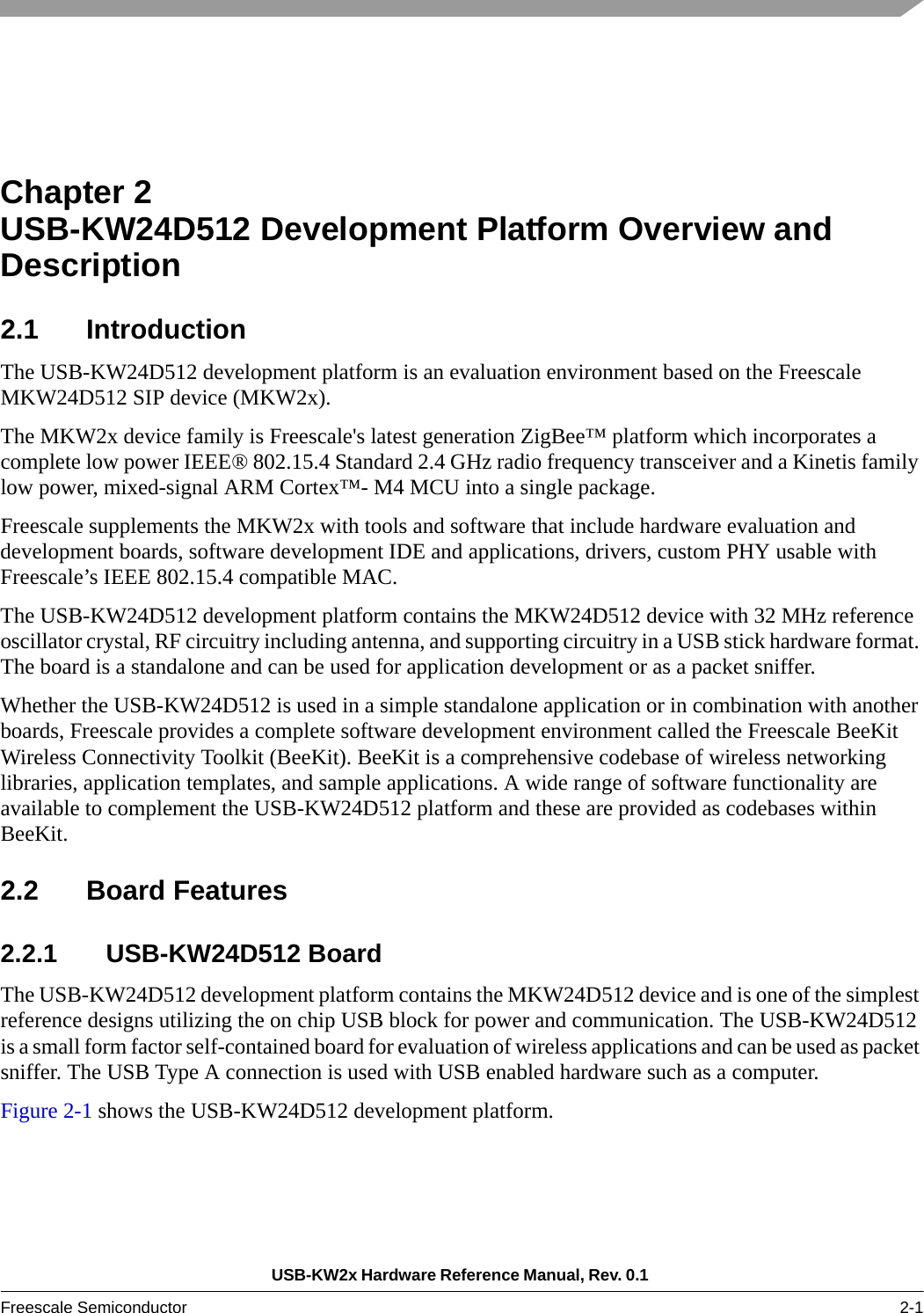
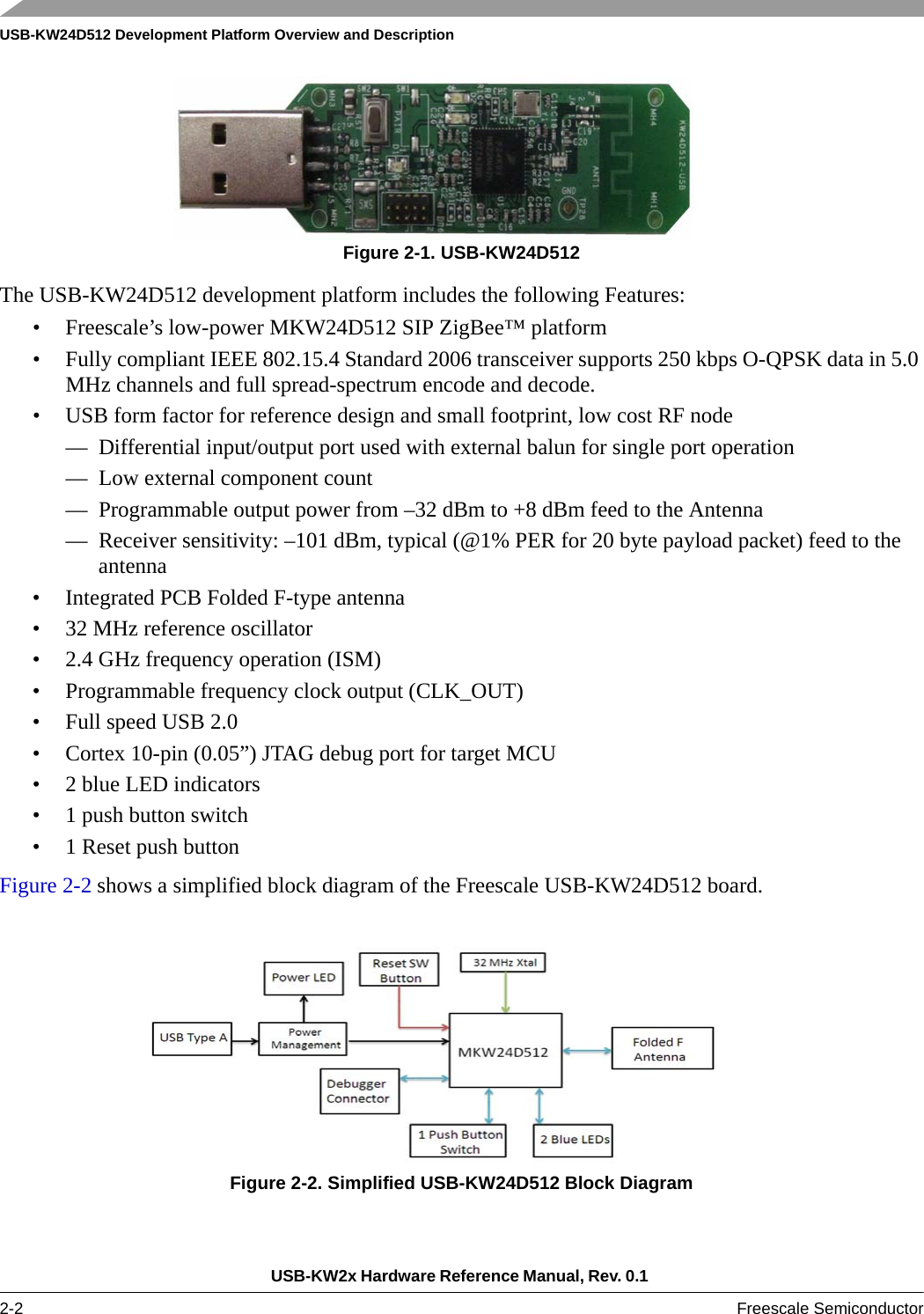
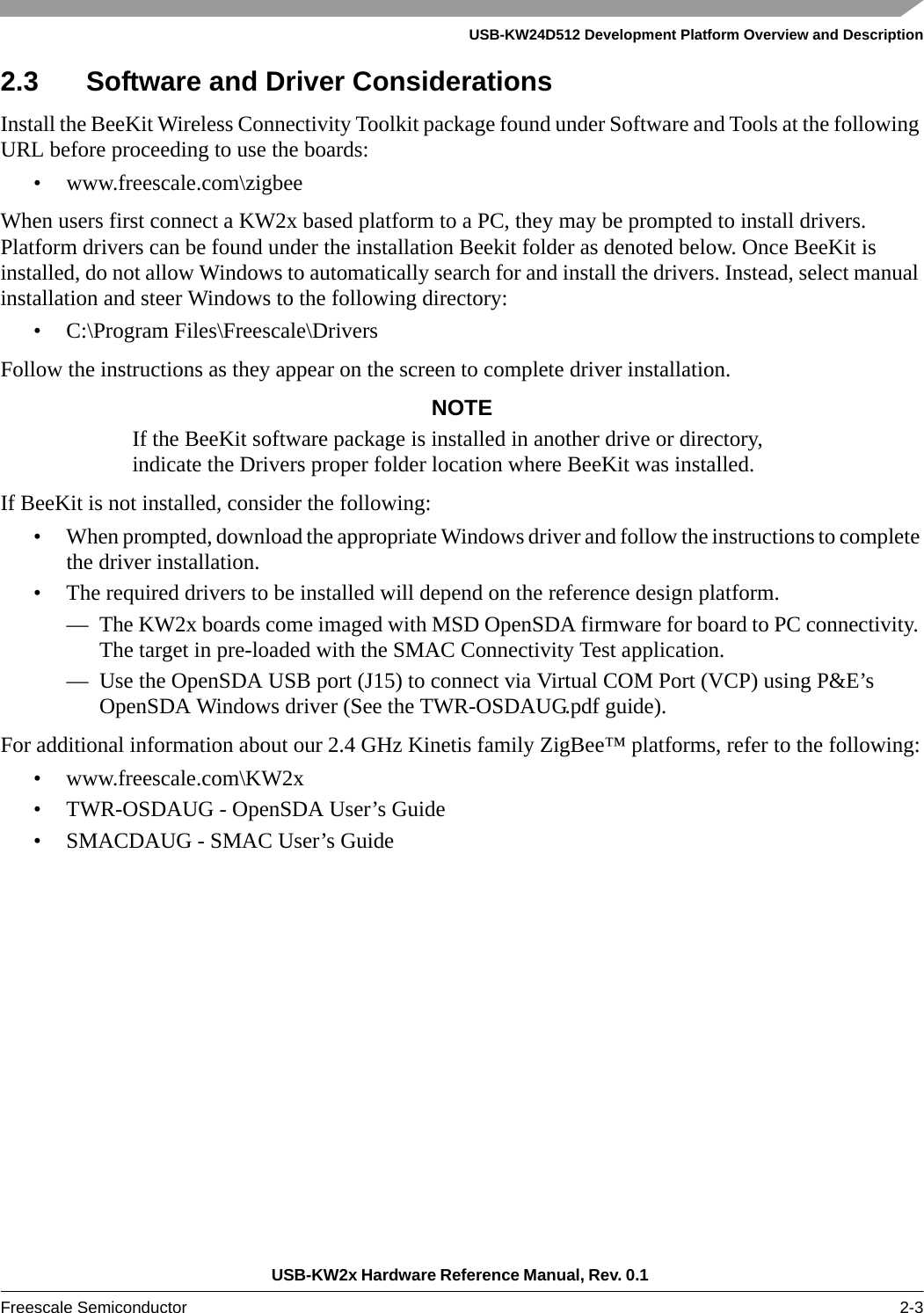
Freescale Semiconductor USBKW24D USB Dongle User Manual USB KW2x Hardware Reference Manual

Freescale Semiconductor, Inc. USB Dongle USB KW2x Hardware Reference Manual

Contents

Reference Manual

Document Number: USB-KW2XHWRMRev. 0.103/2014 USB-KW2X HardwareReference Manual
How to Reach Us:Home Page:freescale.comWeb Support:freescale.com/supportInformation in this document is provided solely to enable system and software implementers to use Freescale products. There are no express or implied copyright licenses granted hereunder to design or fabricate any integrated circuits based on the information in this document.Freescale reserves the right to make changes without further notice to any products herein. Freescale makes no warranty, representation, or guarantee regarding the suitability of its products for any particular purpose, nor does Freescale assume any liability arising out of the application or use of any product or circuit, and specifically disclaims any and all liability, including without limitation consequential or incidental damages. “Typical” parameters that may be provided in Freescale data sheets and/or specifications can and do vary in different applications, and actual performance may vary over time. All operating parameters, including “typicals,” must be validated for each customer application by customer’s technical experts. Freescale does not convey any license under its patent rights nor the rights of others. Freescale sells products pursuant to standard terms and conditions of sale, which can be found at the following address: freescale.com/SalesTermsandConditions.  Freescale, the Freescale logo, AltiVec, CodeWarrior, ColdFire, ColdFire+,Energy Efficient Solutions logo, PowerQUICC, QorIQ, StarCore, Symphony, and VortiQa are trademarks of Freescale Semiconductor, Inc., Reg. U.S. Pat. & Tm. Off. CoreNet, Layerscape, QorIQ Qonverge, QUICC Engine, Tower, and Xtrinsic are trademarks of Freescale Semiconductor, Inc. All other product or service names are the property of their respective owners. ARM and Cortex are registered trademarks of ARM Limited. ARMnnn is the trademark of ARM Limited.© 2014 Freescale Semiconductor, Inc.
USB-KW2x Hardware Reference Manual, Rev. 0.1Freescale Semiconductor iii  About This BookAudience . . . . . . . . . . . . . . . . . . . . . . . . . . . . . . . . . . . . . . . . . . . . . . . . . . . . . . . . . . . . . . . . . . . . . vOrganization . . . . . . . . . . . . . . . . . . . . . . . . . . . . . . . . . . . . . . . . . . . . . . . . . . . . . . . . . . . . . . . . . . vRevision History . . . . . . . . . . . . . . . . . . . . . . . . . . . . . . . . . . . . . . . . . . . . . . . . . . . . . . . . . . . . . . . vChapter 1Safety Information1.1 FCC Guidelines. . . . . . . . . . . . . . . . . . . . . . . . . . . . . . . . . . . . . . . . . . . . . . . . . . . . . . . . . . . . . .  1-11.1.1 Labeling  . . . . . . . . . . . . . . . . . . . . . . . . . . . . . . . . . . . . . . . . . . . . . . . . . . . . . . . . . . . . . . . .  1-11.1.2 Operating Conditions . . . . . . . . . . . . . . . . . . . . . . . . . . . . . . . . . . . . . . . . . . . . . . . . . . . . . .  1-11.1.3 Exposure Limits . . . . . . . . . . . . . . . . . . . . . . . . . . . . . . . . . . . . . . . . . . . . . . . . . . . . . . . . . .  1-11.1.4 Antenna Restrictions. . . . . . . . . . . . . . . . . . . . . . . . . . . . . . . . . . . . . . . . . . . . . . . . . . . . . . .  1-11.2 Regulatory Approval For Canada (IC RSS 210)  . . . . . . . . . . . . . . . . . . . . . . . . . . . . . . . . . . . .  1-21.2.1 26 PART 5 – Appendix  . . . . . . . . . . . . . . . . . . . . . . . . . . . . . . . . . . . . . . . . . . . . . . . . . . . .  1-21.3 Electrostatic Discharge Considerations  . . . . . . . . . . . . . . . . . . . . . . . . . . . . . . . . . . . . . . . . . . . 1-21.4 Disposal Instructions. . . . . . . . . . . . . . . . . . . . . . . . . . . . . . . . . . . . . . . . . . . . . . . . . . . . . . . . . .  1-2Chapter 2USB-KW24D512 Development Platform Overview and Description2.1 Introduction. . . . . . . . . . . . . . . . . . . . . . . . . . . . . . . . . . . . . . . . . . . . . . . . . . . . . . . . . . . . . . . . .  2-12.2 Board Features  . . . . . . . . . . . . . . . . . . . . . . . . . . . . . . . . . . . . . . . . . . . . . . . . . . . . . . . . . . . . . .  2-12.2.1 USB-KW24D512 Board. . . . . . . . . . . . . . . . . . . . . . . . . . . . . . . . . . . . . . . . . . . . . . . . . . . .  2-12.3 Software and Driver Considerations. . . . . . . . . . . . . . . . . . . . . . . . . . . . . . . . . . . . . . . . . . . . . . 2-3Chapter 3USB-KW24D5123.1 USB-KW24D512 Overview. . . . . . . . . . . . . . . . . . . . . . . . . . . . . . . . . . . . . . . . . . . . . . . . . . . . 3-13.1.1 PCB Board Features . . . . . . . . . . . . . . . . . . . . . . . . . . . . . . . . . . . . . . . . . . . . . . . . . . . . . . .  3-13.1.2 Form Factor. . . . . . . . . . . . . . . . . . . . . . . . . . . . . . . . . . . . . . . . . . . . . . . . . . . . . . . . . . . . . .  3-13.1.3 Board Level Specifications. . . . . . . . . . . . . . . . . . . . . . . . . . . . . . . . . . . . . . . . . . . . . . . . . .  3-23.2 Functional Description . . . . . . . . . . . . . . . . . . . . . . . . . . . . . . . . . . . . . . . . . . . . . . . . . . . . . . . .  3-33.2.1 RF Performance and Considerations  . . . . . . . . . . . . . . . . . . . . . . . . . . . . . . . . . . . . . . . . . .  3-43.2.2 Clocks . . . . . . . . . . . . . . . . . . . . . . . . . . . . . . . . . . . . . . . . . . . . . . . . . . . . . . . . . . . . . . . . . .  3-53.2.3 Power Management  . . . . . . . . . . . . . . . . . . . . . . . . . . . . . . . . . . . . . . . . . . . . . . . . . . . . . . .  3-53.2.4 USB-KW24D512 Peripheral Functions . . . . . . . . . . . . . . . . . . . . . . . . . . . . . . . . . . . . . . . .  3-63.3 Schematic, Board Layout, and Bill of Material . . . . . . . . . . . . . . . . . . . . . . . . . . . . . . . . . . . . .  3-73.3.1 Bill of Materials . . . . . . . . . . . . . . . . . . . . . . . . . . . . . . . . . . . . . . . . . . . . . . . . . . . . . . . . . .  3-9Chapter 4PCB Manufacturing Specifications4.1 Single PCB Construction . . . . . . . . . . . . . . . . . . . . . . . . . . . . . . . . . . . . . . . . . . . . . . . . . . . . . .  4-14.2 Panelization. . . . . . . . . . . . . . . . . . . . . . . . . . . . . . . . . . . . . . . . . . . . . . . . . . . . . . . . . . . . . . . . .  4-2
USB-KW2x Hardware Reference Manual, Rev. 0.1iv Freescale Semiconductor  4.3 Materials . . . . . . . . . . . . . . . . . . . . . . . . . . . . . . . . . . . . . . . . . . . . . . . . . . . . . . . . . . . . . . . . . . .  4-24.4 Solder Mask . . . . . . . . . . . . . . . . . . . . . . . . . . . . . . . . . . . . . . . . . . . . . . . . . . . . . . . . . . . . . . . .  4-34.5 Silk Screen  . . . . . . . . . . . . . . . . . . . . . . . . . . . . . . . . . . . . . . . . . . . . . . . . . . . . . . . . . . . . . . . . .  4-34.6 Electrical PCB Testing . . . . . . . . . . . . . . . . . . . . . . . . . . . . . . . . . . . . . . . . . . . . . . . . . . . . . . . .  4-34.7 Packaging . . . . . . . . . . . . . . . . . . . . . . . . . . . . . . . . . . . . . . . . . . . . . . . . . . . . . . . . . . . . . . . . . .  4-34.8 Hole Specification/Tool Table . . . . . . . . . . . . . . . . . . . . . . . . . . . . . . . . . . . . . . . . . . . . . . . . . .  4-34.9 File Description. . . . . . . . . . . . . . . . . . . . . . . . . . . . . . . . . . . . . . . . . . . . . . . . . . . . . . . . . . . . . .  4-4
USB-KW2x  Hardware Reference Manual, Rev. 0.1 Freescale Semiconductor v About This BookThis manual describes Freescale’s MKW2xDxxx development platform hardware. The MKW2xDxxx is an IEEE® 802.15.4 compliant evaluation environment based on the Freescale MKW2xDxxx device. The MKW2xDxxx family is Freescale's latest generation ZigBee™ platform, which incorporates a complete low power 2.4 GHz radio frequency transceiver and a Kinetis family low power, mixed-signal ARMR eCortex™- M4 MCU into a single package. This family of products is targeted to meet the higher performance requirements of ZigBee Pro and ZigBee IP based applications, especially Smart Energy and Commercial Building Automation. This product is a cost-effective solution that matches or exceeds competitive solutions.AudienceThis manual is intended for system designers.OrganizationThis document is organized into the following chapters.Chapter 1 Safety Information — Highlights some of the FCC requirements.Chapter 2 MKW2xDxxx Development Platform Overview and Description — Provides an overview of the boards that comprise the MKW2xDxxx development platform.Chapter 3 USB-KW24D512 — This chapter details the USB-KW24D512 evaluation board.Chapter 4 PCB Manufacturing Specifications — This chapter provides the specifications used to manufacture the various MKW2xDxxx printed circuit boards (PCBs).Revision HistoryThe following table summarizes revisions to this document since the previous release (Rev. 0.0).Revision HistoryLocation RevisionEntire document First public releaseEntire document Rev. 0.1, Rename KW24512-USB to USB-KW24D512 development board.
USB-KW2x  Hardware Reference Manual, Rev. 0.1 vi Freescale Semiconductor Definitions, Acronyms, and AbbreviationsThe following list defines the acronyms and abbreviations used in this document. ADC Analog to Digital ConverterAES Advanced Encryption StandardCTS Clear to SendDAC Digital to Analog ConverterI2C Inter-Integrated Circuit is a multi-master serial computer busISM Industrial Scientific Medical 2.4 GHz radio frequency bandJTAG Joint Test Action GroupLGA Land Grid ArrayMAC Media Access ControllerMCU Microcontroller UnitPCB Printed circuit boardPiP Platform in PackagePWM Pulse-width modulation RCM Remote Control ModuleREM Remote Extender BoardRTS Request to SendSMA Connector SubMiniature version “A” connector SoC System on ChipSPI Serial Peripheral InterfaceSSI Synchronous Serial InterfaceTACT Switch A switch that provides a slight “snap” or “click” to the user to indicate function.TELCO Telephone CompanyTWR Tower SystemUSB Universal Serial BusVCP Virtual Com Port
USB-KW2x Hardware Reference Manual, Rev. 0.1 Freescale Semiconductor 1-1Chapter 1  Safety Information1.1 FCC GuidelinesThis equipment is for use by developers for evaluation purposes only and must not be incorporated into any other device or system. This device may not be sold to the general public. Integrators will be responsible for reevaluating the end product (including the transmitter) and obtaining a separate FCC authorization.FCC approval of this device only covers the original configuration of this device as supplied. Any modifications to this product, including changes shown in this manual, may violate the rules of the Federal Communications Commission and Industry Canada and make operation of the product unlawful.1.1.1 LabelingFCC labels are physically located on the back of the board.1.1.2 Operating ConditionsThis device complies with part 15 of the FCC Rules. Operation is subject to the following two conditions:• This device may not cause harmful interference.• This device must accept any interference received, including interference that may cause undesired operation.1.1.3 Exposure LimitsThis equipment complies with FCC radiation exposure limits set forth for an uncontrolled environment. The antenna(s) used for this equipment must be installed to provide a separation distance of at least 8 inches (20cm) from all persons.1.1.4 Antenna RestrictionsAn intentional radiator is designed to ensure that no antenna other than that furnished by the responsible party is used with the device. The use of a permanently attached antenna or of an antenna that uses a unique coupling to the intentional radiator is considered sufficient to comply with the provisions of this Section. The manufacturer may design the unit so that a broken antenna can be replaced by the user, but the use of a standard antenna jack or electrical connector is prohibited. This requirement does not apply to carrier current devices or to devices operated under the provisions of Sections 15.211, 15.213, 15.217, 15.219, or 15.221. Further, this requirement does not apply to intentional radiators that must be professionally
Safety InformationUSB-KW2x Hardware Reference Manual, Rev. 0.1 1-2 Freescale Semiconductorinstalled, such as perimeter protection systems and some field disturbance sensors, or to other intentional radiators which, in accordance with Section 15.31(d), must be measured at the installation site. However, the installer is responsible for ensuring that the proper antenna is employed so that the limits in this Part are not exceeded. 1.2 Regulatory Approval For Canada (IC RSS 210)This device complies with Industry Canada licence-exempt RSS standard(s). Operation is subject to the following two conditions:1. This device may not cause interference, and 2. This device must accept any interference, including interference that may cause undesired operation of the device.1.2.1 26 PART 5 – AppendixLe présent appareil est conforme aux CNR d'Industrie Canada applicables aux appareils radio exempts de licence. L'exploitation est autorisée aux deux conditions suivantes: 1. l'appareil ne doit pas produire de brouillage, et 2. l'utilisateur de l'appareil doit accepter tout brouillage radioélectrique subi, même si le brouillage est susceptible d'en compromettre le fonctionnement. 1.3 Electrostatic Discharge ConsiderationsAlthough damage from electrostatic discharge (ESD) is much less common on these devices than on early CMOS circuits, normal handling precautions should be used to avoid exposure to static discharge. Qualification tests are performed to ensure that these devices can withstand exposure to reasonable levels of static without suffering any permanent damage.All ESD testing is in conformity with the JESD22 Stress Test Qualification for Commercial Grade Integrated Circuits. During the device qualification ESD stresses were performed for the human body model (HBM), the machine model (MM) and the charge device model (CDM).All latch-up test testing is in conformity with the JESD78 IC Latch-Up Test.When operating or handling the development boards or components, Freescale strongly recommends using at least the grounding wrist straps plus any or all of the following ESD dissipation methods:• Flexible fabric, solid fixed size, or disposable ESD wrist straps• Static control workstations, static control monitors and table or floor static control systems• Static control packaging and transportation materials and environmental systems1.4 Disposal InstructionsThis product may be subject to special disposal requirements. For product disposal instructions, refer to www.freescale.com/productdisposal.
USB-KW2x Hardware Reference Manual, Rev. 0.1 Freescale Semiconductor 2-1Chapter 2  USB-KW24D512 Development Platform Overview and Description2.1 IntroductionThe USB-KW24D512 development platform is an evaluation environment based on the Freescale MKW24D512 SIP device (MKW2x).The MKW2x device family is Freescale's latest generation ZigBee™ platform which incorporates a complete low power IEEE® 802.15.4 Standard 2.4 GHz radio frequency transceiver and a Kinetis family low power, mixed-signal ARM Cortex™- M4 MCU into a single package.Freescale supplements the MKW2x with tools and software that include hardware evaluation and development boards, software development IDE and applications, drivers, custom PHY usable with Freescale’s IEEE 802.15.4 compatible MAC.The USB-KW24D512 development platform contains the MKW24D512 device with 32 MHz reference oscillator crystal, RF circuitry including antenna, and supporting circuitry in a USB stick hardware format. The board is a standalone and can be used for application development or as a packet sniffer.Whether the USB-KW24D512 is used in a simple standalone application or in combination with another boards, Freescale provides a complete software development environment called the Freescale BeeKit Wireless Connectivity Toolkit (BeeKit). BeeKit is a comprehensive codebase of wireless networking libraries, application templates, and sample applications. A wide range of software functionality are available to complement the USB-KW24D512 platform and these are provided as codebases within BeeKit.2.2 Board Features2.2.1 USB-KW24D512 BoardThe USB-KW24D512 development platform contains the MKW24D512 device and is one of the simplest reference designs utilizing the on chip USB block for power and communication. The USB-KW24D512 is a small form factor self-contained board for evaluation of wireless applications and can be used as packet sniffer. The USB Type A connection is used with USB enabled hardware such as a computer.Figure 2-1 shows the USB-KW24D512 development platform.
USB-KW24D512 Development Platform Overview and DescriptionUSB-KW2x Hardware Reference Manual, Rev. 0.1 2-2 Freescale SemiconductorFigure 2-1. USB-KW24D512The USB-KW24D512 development platform includes the following Features:• Freescale’s low-power MKW24D512 SIP ZigBee™ platform• Fully compliant IEEE 802.15.4 Standard 2006 transceiver supports 250 kbps O-QPSK data in 5.0 MHz channels and full spread-spectrum encode and decode.• USB form factor for reference design and small footprint, low cost RF node— Differential input/output port used with external balun for single port operation— Low external component count — Programmable output power from –32 dBm to +8 dBm feed to the Antenna— Receiver sensitivity: –101 dBm, typical (@1% PER for 20 byte payload packet) feed to the antenna• Integrated PCB Folded F-type antenna• 32 MHz reference oscillator• 2.4 GHz frequency operation (ISM)• Programmable frequency clock output (CLK_OUT)• Full speed USB 2.0 • Cortex 10-pin (0.05”) JTAG debug port for target MCU• 2 blue LED indicators• 1 push button switch• 1 Reset push buttonFigure 2-2 shows a simplified block diagram of the Freescale USB-KW24D512 board.Figure 2-2. Simplified USB-KW24D512 Block Diagram
USB-KW24D512 Development Platform Overview and DescriptionUSB-KW2x Hardware Reference Manual, Rev. 0.1 Freescale Semiconductor 2-32.3 Software and Driver ConsiderationsInstall the BeeKit Wireless Connectivity Toolkit package found under Software and Tools at the following URL before proceeding to use the boards:• www.freescale.com\zigbeeWhen users first connect a KW2x based platform to a PC, they may be prompted to install drivers. Platform drivers can be found under the installation Beekit folder as denoted below. Once BeeKit is installed, do not allow Windows to automatically search for and install the drivers. Instead, select manual installation and steer Windows to the following directory:• C:\Program Files\Freescale\DriversFollow the instructions as they appear on the screen to complete driver installation.NOTEIf the BeeKit software package is installed in another drive or directory, indicate the Drivers proper folder location where BeeKit was installed.If BeeKit is not installed, consider the following:• When prompted, download the appropriate Windows driver and follow the instructions to complete the driver installation.• The required drivers to be installed will depend on the reference design platform.— The KW2x boards come imaged with MSD OpenSDA firmware for board to PC connectivity. The target in pre-loaded with the SMAC Connectivity Test application.— Use the OpenSDA USB port (J15) to connect via Virtual COM Port (VCP) using P&E’s OpenSDA Windows driver (See the TWR-OSDAUG.pdf guide).For additional information about our 2.4 GHz Kinetis family ZigBee™ platforms, refer to the following:• www.freescale.com\KW2x• TWR-OSDAUG - OpenSDA User’s Guide• SMACDAUG - SMAC User’s Guide
USB-KW24D512 Development Platform Overview and DescriptionUSB-KW2x Hardware Reference Manual, Rev. 0.1 2-4 Freescale Semiconductor
USB-KW2x Hardware Reference Manual, Rev. 0.1 Freescale Semiconductor 3-1Chapter 3  USB-KW24D5123.1 USB-KW24D512 OverviewThe USB-KW24D512 is an evaluation board based on the Freescale MKW24D512 device. The USB-KW24D512 provides a platform to evaluate the USB-KW24D512 SIP IC, develop software and applications. The core device is accompanied by the 32 MHz reference oscillator crystal, RF circuitry including a printed board antenna, and supporting circuitry.This basic board is intended as the core PCB for USB-KW24D512 evaluation and application development and can be used as a simple standalone evaluation solution or use a packet sniffer.3.1.1 PCB Board FeaturesThe USB-KW24D512 provides the following features:• USB small form factor • 4-Layer metal, 0.062 inch thick FR4 board• LGA footprint and power supply bypass• Printed metal folded F-Antenna• 32 MHz reference oscillator crystal3.1.2 Form FactorFigure 3-1 shows the USB-KW24D512 connector and header locations.Figure 3-1. USB-KW24D512 Figure 3-2 shows a footprint of the USB-KW24D512 with the location of the header and connectors
USB-KW24D512USB-KW2x Hardware Reference Manual, Rev. 0.1 3-2 Freescale Semiconductor Figure 3-2. USB-KW24D512 Top Side (Component Side) Footprint3.1.3 Board Level SpecificationsTable 3-1. USB-KW24D512 SpecificationsParameter Min Typ Max Units Notes/ConditionsGeneralSize (PCB: X, Y) 61.4 x 18.52.42 x 0.73mminchesLayer build (PCB) 1.570.062mminches4-LayerDielectric material (PCB) FR4PowerCurrent consumption mA Refer to datasheetTemperatureOperating temperature (see note) -40 +25 +70 °C  • Operating temperature is limited to +70 °C due to switches. Basic circuit is good for a maximum temperature of +85 °C.Storage temperature -30 +25 +70 °CRF 802.15.4 Frequency range 2405 2480 MHzAll 16 channels in the2450 MHz bandRF ReceiverSaturation (maximum input level) +10 dBm DatasheetSensitivity for 1% packet error rate (PER) (+25 °C) -102 dBm DatasheetRF Transmitter
USB-KW24D512USB-KW2x Hardware Reference Manual, Rev. 0.1 Freescale Semiconductor 3-33.2 Functional DescriptionThe USB-KW24D512 is built around Freescale’s MKW24D512 63-pin (56-pin usable) LGA platform. This board is intended as a simple evaluation platform and as a building block for application development. The 4-layer board provides the MKW24D512 with its required RF circuitry, 32 MHz reference oscillator crystal, and power supply bypassing. The layout for this base level functionality can be used as a reference layout by the user target board. Figure 3-3 shows a simple block diagram. RF Power Output  -32 +8 dBm Programmable in 2dB steps.At the antenna feed with no trap. 1.2nd harmonic <-50 <-40 dBm Datasheet3rd harmonic <-50 <-40 dBm DatasheetRegulatory ApprovalFCC Product is approved accordingly to the FCC part 15 standardCE (ETSI) Product is approved accordingly to the EN 300 328 V1.7.1 (2006-10) standardCE (EMC) Product is approved accordingly to the EN 301 489-1 V1.6.1 (2005-09) and EN 301 489-17 V1.2.1 (2002-08) standardsSafetyUL Product is approved accordingly to the IEC 60950-1 and EN 60950-1, First Edition standardsEnvironmentRoHS Product complies with the EU Directive 2002/95/EC of 27 January 2003WEEE Product complies with the EU Directive 2002/95/EC of 27 January 20031Trap will add 1 to 2 dB of loss.Table 3-1. USB-KW24D512 Specifications (continued)Parameter Min Typ Max Units Notes/Conditions
USB-KW24D512USB-KW2x Hardware Reference Manual, Rev. 0.1 3-4 Freescale SemiconductorFigure 3-3. USB-KW24D512 Block Diagram3.2.1 RF Performance and ConsiderationsUSB-KW24D512 transceiver includes a 1mW nominal output power, PA with internal voltage controlled oscillator (VCO), integrated transmit/receive switch, on-board power supply regulation, and full spread-spectrum encoding and decoding. The USB-KW24D512 utilizes a minimum number of components while providing good RF performance. Key specifications for USB-KW24D512 are: • Nominal output power is set to 0 dBm• Programmable output power from –32 dBm to +8 dBm measured at the antenna feed• Typical sensitivity is -101 dBm (@1% PER for 25 °C) measured at the antenna feed• Frequency range is 2360 to 2480 MHz• Folded “F” printed metal antenna for a small footprint, low cost design• Uses a minimum number of RF marching components and external 50:50 balunAn external 50 (unbal): 50(bal) balun connects a single-ended 50-ohm port to the differential RF port of the MKW24D512 radio. The layout has provision for out-of-band signal suppression (components L5 and C19) if required. Figure 3-4 shows the typical topology for the RF circuitry. The RF switch J4 has been designed in for measurement purposes and is left as DNP.Figure 3-4. USB-KW24D512 RF Circuitry
USB-KW24D512USB-KW2x Hardware Reference Manual, Rev. 0.1 Freescale Semiconductor 3-53.2.2 ClocksThe USB-KW24D512 provides one clock:• 32 MHz Reference Oscillator — Figure 3-5 shows the external 32 MHz external crystal Y1. This mounted crystal must meet the specifications outlined in the AN3251 application note. The IEEE 802.15.4 Standard requires that the frequency be accurate to less that +/-40 ppm.— Capacitors C10 and C11 provide the bulk of the crystal load capacitance. Onboard trim capacitors can be programmed to center the frequency. At 25°C, it is desired to have the frequency accurate to +/-10 ppm or less to allow for temperature variation.— To measure the 32 MHz oscillator frequency, signal CLK_OUT (TP5) can optionally be programmed to provide a buffered output clock signal. Figure 3-5. USB-KW24D512 32 MHz Reference Oscillator Circuit3.2.3 Power ManagementThe USB-KW24D512 power management circuit is shown in Figure 3-6.
USB-KW24D512USB-KW2x Hardware Reference Manual, Rev. 0.1 3-6 Freescale SemiconductorFigure 3-6. USB-KW24D512 Power Management CircuitThe USB-KW24D512 is powered via the USB type A connector as shown in Figure 3-6., “USB-KW24D512 Power Management Circuit”; the MKW24D512 device has an on-board USB port which is configured to provide both power and serial communication with the target MCU.3.2.4 USB-KW24D512 Peripheral FunctionsThe USB-KW24D512 includes two switch buttons; one for general purpose peripheral function to assist in implementing targeted applications and the other is for board hardware Reset.In the same situation the USB-KW24D512 includes two LEDs for general purpose peripheral function to assist on applications.
USB-KW24D512USB-KW2x Hardware Reference Manual, Rev. 0.1 Freescale Semiconductor 3-7 3.3 Schematic, Board Layout, and Bill of MaterialFigure 3-7. USB-KW24D512 Schematic5544332211D DC CB BA AHARMONIC TRAP32MHz XTALLED VOLTAGEMCU VOLTAGERF VOLTAGEPIN FUNCTIONS USED NET NAMESJTAG / SWD CONNECTORPOWER MANAGEMENTPOWER ONRESETIN CIRCUIT TEST GND PROBINGCLK_OUTPTC4_RPTD4PTD5PTA1PTA2PTA3PTA0TAMPER0RST_TGTMCU_BXTAL_32MVREFLEXTAL_32MZ_RF_NZ_RF_PRF_OUTNRF_OUTPRF_50VREFHPTC4TP_ANT_ATP_ANT_BVDD_PAVDD_IFVDD_RFVDD_REGDVDD_REGDBAL_CKW24_USB_DPKW24_USB_DNKW24_USB_DPKW24_USB_DNXTAL_32MEXTAL_32MUSB_DPV_USB_CONN V_USB_CONN_INDUSB_DNRST_TGTMCU_BPTD4_LEDPTD5_LEDPTD4PTD5PTC4PTA1JTAG_TDI/EZP_DIPTA2JTAG_TDO/TRACE_SWO/EZP_DOPTA0JTAG_TCLK/SWD_CLK/EZP_CLKPTA3JTAG_TMS/SWD_DIOK24_USB_SHLDTP_RX_SWITCHTP_TX_SWITCHLED_PWR_RVDD_IFVDD_RF VDD_PARF_ANTRST_TGTMCU_BV_MCUV_MCUV_MCUV_RFV_MCUV_MCUV_LEDV_LEDV_MCUV_RFV_MCUV_USBV_USB3V33V3V_LEDV_MCUGNDDrawing Title:Size Document Number RevDate: Sheet ofPage Title:ICAP Classification: FCP: FIUO: PUBI:AX-KW24D512-USBCFriday, August 30, 2013MAIN SCHEMATIC33___ ___XSCH-28057 PDF: SPF-28057Drawing Title:Size Document Number RevDate: Sheet ofPage Title:ICAP Classification: FCP: FIUO: PUBI:AX-KW24D512-USBCFriday, August 30, 2013MAIN SCHEMATIC33___ ___XSCH-28057 PDF: SPF-28057Drawing Title:Size Document Number RevDate: Sheet ofPage Title:ICAP Classification: FCP: FIUO: PUBI:AX-KW24D512-USBCFriday, August 30, 2013MAIN SCHEMATIC33___ ___XSCH-28057 PDF: SPF-28057TP18TP7L5330 OHM1 2U1MKW24D512VVDD_MCU 20VDDA 25VREFH 26VREFL 27VSSA 28VBAT_MCU 32VDD_MCU 38VBAT2_RF 42VDD_REGD 43VDD_PA 52VDD_IF 53VDD_RF 54GND_PA363GND_PA148GND_PA251EXTAL_32M1TAMPER0/RT C_W AKEUP29XTAL3230EXTAL3231RESET41RX_SWITCH46TX_SWITCH47RF_OUTP 49RF_OUTN 50XTAL_32M56GPIO12GPIO23PTA0/JTAG_TCLK/SWD_CLK/EZP_CLK/UART0_CTS/UART0_COL/FTM0_CH533PTA1/JTAG_T DI/EZP_DI/UART 0_RX/FT M0_CH634PTA2/JTAG_T DO/TRACE_SW O/EZP_DO/UART0_TX/FT M0_CH735PTA3/JTAG_TMS/SWD_DIO/UART0_RTS/FTM0_CH036PTA4/LLWU_P3/NMI/EZP_CS/FTM0_CH137PTA18/EXTAL0/FTM0_FLT2/FTM_CLKIN039PTA19/XTAL0/FT M1_FLT0/FTM_CLKIN1/LPTMR0_ALT140PTC4/LLW U_P8/SPI0_PCS0/UART1_TX/FTM0_CH3/CMP1_OUT4PTC5/LLW U_P9/SPI0_SCK/LPTMR0_ALT2/I2S0_RXD0/CMP0_OUT5PTC6/LLW U_P10/CMP0_IN0/SPI0_SOUT/PDB0_EXTRG/I2S0_RX_BCLK/I2S0_MCLK6PTC7/CMP0_IN1/SPI0_SIN/USB_SOF_OUT/I2S0_RX_FS7PTD1/ADC0_SE5B/SPI0_SCK/UART2_CTS 8PTD2/LLW U_P13/SPI0_SOUT/UART2_RX/I2C_SCL/GPIO4_BSM_DATA 9PTD3/SPI0_SIN/UART2_T X/I2C_SDA/GPIO5_BSM_CLK 10PTD4/LLW U_P14/MADC0_SE21/SPI0_PCS1/UART0_RTS/FTM0_CH4/EW M_IN/GPIO_BSM_FRAME 11PTD5/ADC0_SE6B/SPI0_PCS2/UART0_CTS/UART0_COL/FTM0_CH5/EWM_OUT 12PTD6/LLW U_P15/ADC0_SE7B/SPI0_PCS3/UART0_RX/FTM0_CH6/FTM0_FLT0 13PTD7/MADC0_SE22/CMT_IRO/UART0_TX/FTM0_CH7/FTM0_FLT1 14PTE0/MADC0_SE10/SPI1_PCS1/UART1_TX/MTRACE_CLKOUT/I2C1_SDA/RTC_CLKOUT 15PTE1/LLWU_P0/MADC0_SE11/SPI1_SOUT/UART1_RX/MTRACE_D3/I2C1_SCL/SPI1_SIN 16USB0_DP 21USB0_DM 22VOUT33 23VREGIN 24PTE2/LLWU_P1/MADC0_DP1/SPI1_SCK/UART1_CTS/MTRACE_D2 17PTE3/MADC0_DM1/SPI1_SIN/UART1_RTS/MTRACE_D1/SPI1_SOUT 18PTE4/LLWU_P2/SPI1_PCS0/MTRACE_D0 19EP_GND164EP_GND265NC_57 57NC_58 58NC_59 59NC_60 60NC_61 61NC_62 62VBAT_RF 55ANT_A 44ANT_B 45TP14R14330C1011pF TP8C1111pFL32.2nH12TP3MH1MH_50mil11C45pF C1233PFC90.1UFC292.2UFTP15C201.8pFTP6D3BLUEACC1910PFC130.33UFSH20TP16TP10R20VD-D+GJ5USB_TYPE_AS1A1A2A3A4S2TP4C241000pFZ12400MHz 50OHM516234TP1TP9TP19C265pFR1310KDNPR120ANT1MEANDER_ANT_HORZ21C280.1UFTP2R11.0MC1810PFTP17C80.1UFMH2MH_50mil11R11 0R30TP11C2747PFDNPC15pFY132MHZ1 432C30.33UFMH3MH_50mil11OUTINPROBEJ4MM8030-2600BDNP1432SH30L460OHM1 2TP12SH10R7 33 C211.0UFTP13C21000pFC2547PFDNPC70.1UFDNPD2BLUEACMH4MH_50mil11R8 33TP28DNPC150.33UFSW1SKQYAFE010DNP12C51000pFR9390TP5C171PFRT1MINISMDC050F-21 2SW2SKQYAFE01012J1HDR 2X51 23 4657 8910C1633PFR10390R610KD1GREENACC60.1UF
USB-KW24D512USB-KW2x Hardware Reference Manual, Rev. 0.1 3-8 Freescale SemiconductorFigure 3-8. USB-KW24D512 Reference Board PCB Component Location (Top View)Figure 3-9. USB-KW24D512 Reference Board PCB Test PointsFigure 3-10. USB-KW24D512 Reference Board PCB Layout (Top View)
USB-KW24D512USB-KW2x Hardware Reference Manual, Rev. 0.1 Freescale Semiconductor 3-9Figure 3-11. USB-KW24D512 Reference Board PCB Layout (Bottom View)3.3.1 Bill of MaterialsTable 3-2. Bill of Materials (Common parts for all frequency bands) (Sheet 1 of 3)Item Qty Reference Value Description Mfg. Name Mfg. Part Number1 1 ANT1 MEANDER_ANT_HORZPCB MEANDER ANTENNA HORIZONTAL, NO PART ORDER2 3 C1,C4,C26 5pF CAP CER 5pF 50V 5% C0G 0402 MURATA GJM1555C1H5R0CB01D3 3 C2,C5,C24 1000pF CAP CER 1000PF 50V 5% C0G 0402MURATA GRM1555C1H102JA01D43C3,C13,C150.33UF CAP CER 0.33UF 6.3V 10% X5R 0402MURATA GRM155R60J334KE01D54C6,C8,C9,C280.1UF CAP CER 0.1UF 16V 10% X7R 0402KEMET C0402C104K4RAC6 1 C7 DNP 0.1UF CAP CER 0.1UF 16V 10% X7R 0402KEMET C0402C104K4RAC7 2 C10,C11 11pF CAP CER 11pF 50V 5% C0G 0402 TDK C1005C0G1H110J8 2 C12,C16 33PF CAP CER 33PF 50V 5% C0G 0402 VENKEL COMPANY C0402C0G500-330JNE9 1 C17 1PF CAP CER 1PF 50V 5% C0G 0402 MURATA GRM1555C1H1R0CA01B10 2 C18,C19 10PF CAP CER 10PF 50V 5% C0G 0402 AVX 04025A100JAT2A11 1 C20 1.8pF CAP CER 1.8PF 50V 0.25PF C0G 0402MURATA GRM1555C1H1R8CA01D12 1 C21 1.0UF CAP CER 1.0UF 10V 10% X5R 0402YAGEO AMERICA CC0402KRX5R6BB105
USB-KW24D512USB-KW2x Hardware Reference Manual, Rev. 0.1 3-10 Freescale Semiconductor13 2 C25,C27 DNP47PF CAP CER 47PF 16V 5% C0G 0402 AVX 0402YA470JAT2A14 1 C29 2.2UF CAP CER 2.2UF 10V 10% X7R 0603TAIYO YUDEN LMK107B7225KA-T15 1 D1 GREEN LED GRN SGL 30MA SMT 0805 LITE ON LTST-C171KGKT16 2 D2,D3 BLUE LED BLUE SGL 20MA SMT 0805 LITE ON LTST-C171TBKT17 1 J1 HDR 2X5 CONN,HEAD,2X5,STR,50/50 CON-2RH-10-50SAMTEC FTS-105-01-F-D18 1 J4 DNP MM8030-2600BCON COAX SMT 1.9MM SP 40H AUMURATA MM8030-2610B19 1 J5 USB_TYPE_ACON 1X4 USB_TYPE_A_MALE RA SMT -- 178H AUSAMTEC USB-AM-S-S-B-SM120 1 L3 2.2nH IND -- 2.2NH@500MHZ 220mA 4% 0402MURATA LQP15MN2N2B0221 1 L4 60OHM IND FER BEAD 60OHM@100MHZ 500MA -- 0603MURATA BLM18PG600SN1D22 1 L5 330 OHM IND FER BEAD 330OHM@100MHZ 2.5A -- SMTTDK MPZ2012S331A23 4 MH1,MH2,MH3,MH4MH_50mil Rework Hole Non-Plated 50mil Drill size 65mil Soldermask TH, NO PART TO ORDER24 1 RT1 MINISMDC050F-2FUSE PLYSW 0.5A 24V SMT TYCO ELECTRONICS MINISMDC050F-225 1 R1 1.0M RES MF 1.0M 1/10W 5% 0603 BOURNS CR0603-JW-105ELF26 4 R2,R3,R11,R120 RES MF ZERO OHM 1/16W 5% 0402ROHM MCR01MZPJ00027 1 R6 10K RES MF 10K 1/10W 5% 0603 KOA SPEER RK73B1JTTD103J28 2 R7,R8 33 RES MF 33 OHM 1/10W 5% 0603 VISHAY INTERTECHNOLOGYCRCW060333R0JNEA29 2 R9,R10 390 RES MF 390 OHM 1/16W 5% 0402 VISHAY INTERTECHNOLOGYCRCW0402390RJNED30 1 R13 DNP 10K RES MF 10K 1/10W 5% 0603 KOA SPEER RK73B1JTTD103J31 1 R14 330 RES MF 330 OHM 1/16W 5% 0402 VISHAY INTERTECHNOLOGYCRCW0402330RJNED32 3 SH1,SH2,SH30 ZERO OHM CUT TRACE 0402 PADS; NO PART TO ORDER33 1 SW1 DNP SKQYAFE010SW SPST MOM PB 50MA 12V SMTALPS ELECTRIC (USA) INC.SKQYAFE01034 1 SW2 SKQYAFE010SW SPST MOM PB 50MA 12V SMTALPS ELECTRIC (USA) INC.SKQYAFE010Table 3-2. Bill of Materials (Common parts for all frequency bands) (Sheet 2 of 3)Item Qty Reference Value Description Mfg. Name Mfg. Part Number
USB-KW24D512USB-KW2x Hardware Reference Manual, Rev. 0.1 Freescale Semiconductor 3-1135 18 TP1,TP2,TP3,TP4,TP5,TP6,TP7,TP8,TP9,TP10,TP11,TP12,TP13,TP14,TP15,TP16,TP17,TP18TPAD_040 TEST POINT PAD 40MIL DIA SMT, NO PART TO ORDER36 1 TP19 TPAD_030 TEST POINT PAD 30MIL DIA SMT, NO PART TO ORDER37 1 TP28 DNP TEST POINT WHITETEST POINT WHITE 40 MIL DRILL 180 MIL TH 109LCOMPONENTS CORPORATIONTP-105-01-0938 1 U1 MKW24D512VIC MCU XCVR 2.4GHZ 64KB RAM 512KB FLASH - USB 1.8-3.6V LGA63Freescale SemiconductorMKW24D512VHA539 1 Y1 32MHZ XTAL 32MHZ 9PF -- SMT 3.2X2.5MMNDK EXS00A-CS0236840 1 Z1 2400MHz 50OHMXFMR BALUN 2400 +/-100MHZ SMT MURATA LDB212G4005C-001Table 3-2. Bill of Materials (Common parts for all frequency bands) (Sheet 3 of 3)Item Qty Reference Value Description Mfg. Name Mfg. Part Number
USB-KW24D512USB-KW2x Hardware Reference Manual, Rev. 0.1 3-12 Freescale Semiconductor
USB-KW2x Hardware Reference Manual, Rev. 0.1 Freescale Semiconductor 4-1Chapter 4  PCB Manufacturing SpecificationsThis chapter provides the specifications used to manufacture the KW2x Development hardware printed circuit board (PCB) described in this manual.The KW2x Development hardware PCBs must comply with the following:• The PCB must comply with Perfag1D/3C (http://www.perfag.dk/Uk/ukindex.htm)• The PCB manufacturer’s logo is required• The PCB production week and year code is required— The manufacturer’s logo and week/year code must be stamped on the back of the PCB solder mask— The PCB manufacturer can not insert text on the PCB either in copper or in silkscreen without written permission from Freescale Semiconductor, Inc.• The required Underwriter’s Laboratory (UL) Flammability Rating— The level is 94V-0 (http://www.ul.com/plastics/flame.html)— The UL information must be stamped on the back of the PCB solder maskNOTE• A complete set of design files is available for the KW2x Development hardware at the Freescale web site (http:www.freescale.com/KW2x) under the “Software and Tools” tab. This design or one of a number of other reference designs should be used as a starting point for a custom application.• The Freescale IEEE 802.15.4 / ZigBee Package and Hardware Layout Considerations Reference Manual, (ZHDCRM) is also available at the same web site to provide additional design guidance.4.1 Single PCB ConstructionThis section describes individual PCB construction details.• The USB-KW24D512 PCB is four-layer, multi layer design• The PCBs contains no blind, buried, or micro vias• PCB data:— USB-KW24D512 Size: Approximately 61.4 x 18.5mm (2.42 x 0.73 inches)— USB-KW24D512 Final thickness (Cu/Cu): 1.57 mm (0.62 inches) +/- 10% (excluding solder mask)
PCB Manufacturing SpecificationsUSB-KW2x Hardware Reference Manual, Rev. 0.1 4-2 Freescale SemiconductorThe following table defines some of the layers of the completed PCB. The artwork identification refers to the name of the layer in commonly used terms.NOTEThe USB-KW24D512 contains high frequency 2.4 GHz RF circuitry. As a result, RF component placement, line geometries and layout, and spacing to the ground plane are critical parameters. As a result, BOARD STACKUP GEOMETRY IS CRITICAL. Dielectric and copper thicknesses and spacing must not be changed; follow the stackup (see Figure 4-1) information is provided with the reference design.Figure 4-1. USB-KW24D512 PCB Stackup Cross-Section (Four Layer)• Solder mask is required• Silk screen is required4.2 PanelizationThe panel size can be negotiated depending on production volume.4.3 MaterialsThe PCB composite materials must meet the following requirements:Table 4-1. USB-KW24D512 Layer by Layer OverviewLayer Artwork Identification  File Name1 Silkscreen Top  SILK_TOP.art2 Top Layer Metal TOP.art3 Ground Layer GND.art4 Power Layer PWR.art5 Bottom Layer Metal BOTTOM.art6 Silkscreen Bottom SILK_BOTTOM.art
PCB Manufacturing SpecificationsUSB-KW2x Hardware Reference Manual, Rev. 0.1 Freescale Semiconductor 4-3• Laminate - The base laminate material (laminate) must be FR4. If the laminate material were changed the RF electrical characteristics may change and degrade RF performance.• Copper Foil - — Top and Bottom copper layers must be 1 oz. copper— Interior layers must be 1oz. copper• Plating - All pad plating must be Hot Air Levelling (HAL)4.4 Solder MaskThe solder mask must meet the following requirements: • Solder mask type: Liquid Film Electra EMP110 or equivalent• Solder mask thickness: 10 – 30 µm4.5 Silk ScreenThe silk screen must meet the following requirements:• Silkscreen color: White• Silkscreen must be applied after application of solder mask if solder mask is required• The silkscreen ink must not extend into any plated-thru-holes• The silk screen must be clipped back to the line of resistance4.6 Electrical PCB Testing• All PCBs must be 100 percent tested for opens and shorts• Impedance Measurement - An impedance measurement report is not mandatory4.7 Packaging Packaging for the PCBs must be the following requirements:• Finished PCBs must remain in panel• Finished PCBs must be packed in plastic bags that do not contain silicones or sulphur materials. These materials can degrade solderability.4.8 Hole Specification/Tool TableSee the ncdrill-1-4.tap file included with the Gerber files and the FAB-28057.pdf file.
PCB Manufacturing SpecificationsUSB-KW2x Hardware Reference Manual, Rev. 0.1 4-4 Freescale Semiconductor4.9 File DescriptionFiles included with the download include Design, Gerber and PDF files. Gerber files are RS-274x format. Not all files included with the Gerber files are for PCB manufacturing.PDF files included are:• FAB-28057.pdf — USB - Board fabrication drawing• GRB-28057.zip — USB - Metal layers, solder mask, solder paste and silk screen• SPF-28057.pdf — USB - SchematicDesign files are in Allegro format with OrCAD schematic capture.

Navigation menu