Freescale Semiconductor ZU Digital Data ZigBee Device User Manual Part 1
Freescale Semiconductor, Inc. Digital Data ZigBee Device Users Manual Part 1
Contents
- 1. Users Manual Part 1
- 2. Users Manual Part 2
Users Manual Part 1

freescale.com
Wireless Sensing Triple Axis Reference design
(ZSTAR) Designer Reference Manual
ZSTARRM
Rev. 0.9
8/2006
Warnings
Safety of Radio Frequency Energy
The manufacturer has evaluated the transmitter for safe operation for uncontrolled use in
the general population. The measured power density at 1 cm is under the threshold
established by the FCC and is not required to be tested for specific absorption rate. The
manufacturer instructs the user that the transmitter should not be handled or placed near
the body continuously for more than 30 minutes while operating.
USA:
NOTE: This equipment has been tested and found to comply with the limits for a Class B
digital device, pursuant to Part 15 of the FCC Rules. These limits are designed to provide
reasonable protection against harmful interference in a residential installation. This
equipment generates, uses and can radiate radio frequency energy and, if not installed
and used in accordance with the instructions, may cause harmful interference to radio
communications. However, there is no guarantee that interference will not occur in a
particular installation. If this equipment does cause harmful interference to radio or
television reception, which can be determined by turning the equipment off and on, the
user is encouraged to try to correct the interference by one or more of the following
measures:
-- Reorient or relocate the receiving antenna.
-- Increase the separation between the equipment and receiver.
-- Connect the equipment into an outlet on a circuit different from that to which the
receiver is connected.
-- Consult the dealer or an experienced radio/TV technician for help.
This device complies with Part 15 of the FCC Rules. Operation is subject to the following
two conditions: (1) this device may not cause harmful interference, and (2) this device
must accept any interference received, including interference that may cause undesired
operation.
Changes or modifications not expressly approved by the party responsible for compliance
could void the user's authority to operate the equipment.
The antenna(s) used for this transmitter must not be co-located or operating in
conjunction with any other antenna or transmitter.
Canada:
This Class [*] digital apparatus complies with Canadian ICES-003.
Cet appareil numériqué de la classe [*] est conformé à la norme NMB-003 du Canada.
Europe:
TBD

Wireless Sensing Triple Axis Reference design, Rev. 0.9
Freescale Semiconductor 3
Wireless Sensing Triple Axis Reference design
Designer Reference Manual
by: Pavel Lajšner and Radomír Kozub
Freescale Czech Systems Laboratories
Rožnov pod RadhoštČm, Czech Republic
To provide the most up-to-date information, the revision of our documents on the World Wide Web will be
the most current. Your printed copy may be an earlier revision. To verify you have the latest information
available, refer to:
http://www.freescale.com
The following revision history table summarizes changes contained in this document. For your
convenience, the page number designators have been linked to the appropriate location.
Revision History
Date Revision
Level Description Page
Number(s)
May,
2006 0.02 First draft N/A
July
2006 0.9 Language correction, minor updates N/A

Revision History
Wireless Sensing Triple Axis Reference design, Rev. 0.9
4 Freescale Semiconductor

Wireless Sensing Triple Axis Reference design, Rev. 0.9
Freescale Semiconductor 5
Table of Contents
Chapter 1
Introduction
1.1 Introduction . . . . . . . . . . . . . . . . . . . . . . . . . . . . . . . . . . . . . . . . . . . . . . . . . . . . . . . . . . . . . . . . . 9
1.2 MMA7260Q 3-axis Accelerometer Sensor. . . . . . . . . . . . . . . . . . . . . . . . . . . . . . . . . . . . . . . . . . 9
Chapter 2
Wireless Sensing Triple Axis Reference design introduction
2.1 Introduction . . . . . . . . . . . . . . . . . . . . . . . . . . . . . . . . . . . . . . . . . . . . . . . . . . . . . . . . . . . . . . . . 11
2.2 Featured products . . . . . . . . . . . . . . . . . . . . . . . . . . . . . . . . . . . . . . . . . . . . . . . . . . . . . . . . . . . 12
2.2.1 Triple Axis Accelerometer MMA7260Q . . . . . . . . . . . . . . . . . . . . . . . . . . . . . . . . . . . . . . . . 12
2.2.2 Microcontroller MC9S08QG8 . . . . . . . . . . . . . . . . . . . . . . . . . . . . . . . . . . . . . . . . . . . . . . . . 12
2.2.3 MC13191 2.4 GHz ISM Band Low Power Transceiver . . . . . . . . . . . . . . . . . . . . . . . . . . . . 13
2.2.4 Microcontroller MCHC908JW32. . . . . . . . . . . . . . . . . . . . . . . . . . . . . . . . . . . . . . . . . . . . . . 13
Chapter 3 Sensor Board description
3.1 Board overview . . . . . . . . . . . . . . . . . . . . . . . . . . . . . . . . . . . . . . . . . . . . . . . . . . . . . . . . . . . . . 15
3.2 A/D conversion of XYZ levels . . . . . . . . . . . . . . . . . . . . . . . . . . . . . . . . . . . . . . . . . . . . . . . . . . 17
3.2.1 ADC module init: . . . . . . . . . . . . . . . . . . . . . . . . . . . . . . . . . . . . . . . . . . . . . . . . . . . . . . . . . 17
3.2.2 ADC measurement. . . . . . . . . . . . . . . . . . . . . . . . . . . . . . . . . . . . . . . . . . . . . . . . . . . . . . . . 18
3.3 Power management. . . . . . . . . . . . . . . . . . . . . . . . . . . . . . . . . . . . . . . . . . . . . . . . . . . . . . . . . . 18
3.3.1 MC13191 power management features. . . . . . . . . . . . . . . . . . . . . . . . . . . . . . . . . . . . . . . . 20
3.4 ZSTAR Sensor Board hardware overview . . . . . . . . . . . . . . . . . . . . . . . . . . . . . . . . . . . . . . . . . 21
3.4.1 Analog connections . . . . . . . . . . . . . . . . . . . . . . . . . . . . . . . . . . . . . . . . . . . . . . . . . . . . . . . 21
3.4.2 g-select connections . . . . . . . . . . . . . . . . . . . . . . . . . . . . . . . . . . . . . . . . . . . . . . . . . . . . . . 21
3.4.3 BDM (Background Debug Mode) connections. . . . . . . . . . . . . . . . . . . . . . . . . . . . . . . . . . . 21
3.4.4 Sensor Board schematics . . . . . . . . . . . . . . . . . . . . . . . . . . . . . . . . . . . . . . . . . . . . . . . . . . 22
3.4.5 Button connections. . . . . . . . . . . . . . . . . . . . . . . . . . . . . . . . . . . . . . . . . . . . . . . . . . . . . . . . 23
3.4.6 MC13191 to MC9S08QG8 microcontroller interface . . . . . . . . . . . . . . . . . . . . . . . . . . . . . . 23
3.4.7 MC13191 RF interface . . . . . . . . . . . . . . . . . . . . . . . . . . . . . . . . . . . . . . . . . . . . . . . . . . . . . 23
3.4.8 Clocking options of MC9S08QG8 . . . . . . . . . . . . . . . . . . . . . . . . . . . . . . . . . . . . . . . . . . . . 24
3.4.9 LED indicators connections . . . . . . . . . . . . . . . . . . . . . . . . . . . . . . . . . . . . . . . . . . . . . . . . . 24
3.4.10 Power supply . . . . . . . . . . . . . . . . . . . . . . . . . . . . . . . . . . . . . . . . . . . . . . . . . . . . . . . . . . . . 25
3.5 Bill of Materials. . . . . . . . . . . . . . . . . . . . . . . . . . . . . . . . . . . . . . . . . . . . . . . . . . . . . . . . . . . . . . 26
Chapter 4 USB stick board description
4.1 Board overview . . . . . . . . . . . . . . . . . . . . . . . . . . . . . . . . . . . . . . . . . . . . . . . . . . . . . . . . . . . . . 27
4.2 ZSTAR USB stick Board hardware overview. . . . . . . . . . . . . . . . . . . . . . . . . . . . . . . . . . . . . . . 30
4.2.1 USB connections . . . . . . . . . . . . . . . . . . . . . . . . . . . . . . . . . . . . . . . . . . . . . . . . . . . . . . . . . 30
4.2.2 Power supply . . . . . . . . . . . . . . . . . . . . . . . . . . . . . . . . . . . . . . . . . . . . . . . . . . . . . . . . . . . . 30
4.2.2.1 Fixed voltage regulators . . . . . . . . . . . . . . . . . . . . . . . . . . . . . . . . . . . . . . . . . . . . . . . . . . 30

Table of Contents
Wireless Sensing Triple Axis Reference design, Rev. 0.9
6 Freescale Semiconductor
4.2.3 MC13191 to MCHC908JW32 microcontroller interface . . . . . . . . . . . . . . . . . . . . . . . . . . . . 31
4.2.4 Oscillator and clocking options. . . . . . . . . . . . . . . . . . . . . . . . . . . . . . . . . . . . . . . . . . . . . . . 31
4.2.5 LED indicators connections . . . . . . . . . . . . . . . . . . . . . . . . . . . . . . . . . . . . . . . . . . . . . . . . . 31
4.2.6 Button connection . . . . . . . . . . . . . . . . . . . . . . . . . . . . . . . . . . . . . . . . . . . . . . . . . . . . . . . . 32
4.2.7 MON08 interface . . . . . . . . . . . . . . . . . . . . . . . . . . . . . . . . . . . . . . . . . . . . . . . . . . . . . . . . . 32
4.2.8 Optional serial interface . . . . . . . . . . . . . . . . . . . . . . . . . . . . . . . . . . . . . . . . . . . . . . . . . . . . 32
4.2.9 USB stick schematics. . . . . . . . . . . . . . . . . . . . . . . . . . . . . . . . . . . . . . . . . . . . . . . . . . . . . . 33
4.3 Bill of Materials. . . . . . . . . . . . . . . . . . . . . . . . . . . . . . . . . . . . . . . . . . . . . . . . . . . . . . . . . . . . . . 34
Chapter 5 Software Design
5.1 Introduction . . . . . . . . . . . . . . . . . . . . . . . . . . . . . . . . . . . . . . . . . . . . . . . . . . . . . . . . . . . . . . . . 35
5.2 SMAC (Simple Media Access Controller) . . . . . . . . . . . . . . . . . . . . . . . . . . . . . . . . . . . . . . . . . 35
5.2.1 SMAC Features . . . . . . . . . . . . . . . . . . . . . . . . . . . . . . . . . . . . . . . . . . . . . . . . . . . . . . . . . . 35
5.2.2 Modifications of SMAC for ZSTAR demo. . . . . . . . . . . . . . . . . . . . . . . . . . . . . . . . . . . . . . . 35
5.2.2.1 MC9S08QG8 SMAC modifications (Sensor Board) . . . . . . . . . . . . . . . . . . . . . . . . . . . . . 36
5.2.2.2 MCHC908JW32 SMAC modifications (USB stick) . . . . . . . . . . . . . . . . . . . . . . . . . . . . . . 36
5.2.2.3 Generic SMAC modifications (USB stick + Sensor Board). . . . . . . . . . . . . . . . . . . . . . . . 37
5.3 ZSTAR RF protocol . . . . . . . . . . . . . . . . . . . . . . . . . . . . . . . . . . . . . . . . . . . . . . . . . . . . . . . . . . 38
5.3.1 Zpacket format . . . . . . . . . . . . . . . . . . . . . . . . . . . . . . . . . . . . . . . . . . . . . . . . . . . . . . . . . . . 38
5.3.1.1 Network number . . . . . . . . . . . . . . . . . . . . . . . . . . . . . . . . . . . . . . . . . . . . . . . . . . . . . . . . 39
5.3.1.2 RX strength. . . . . . . . . . . . . . . . . . . . . . . . . . . . . . . . . . . . . . . . . . . . . . . . . . . . . . . . . . . . 39
5.3.1.3 Zcommand . . . . . . . . . . . . . . . . . . . . . . . . . . . . . . . . . . . . . . . . . . . . . . . . . . . . . . . . . . . . 39
5.3.1.4 Zdata . . . . . . . . . . . . . . . . . . . . . . . . . . . . . . . . . . . . . . . . . . . . . . . . . . . . . . . . . . . . . . . . 39
5.3.2 ZSTAR protocol Zcommand description . . . . . . . . . . . . . . . . . . . . . . . . . . . . . . . . . . . . . . . 40
5.3.2.1 ZSTAR_BROADCAST . . . . . . . . . . . . . . . . . . . . . . . . . . . . . . . . . . . . . . . . . . . . . . . . . . . 40
5.3.2.2 ZSTAR_CONNECT . . . . . . . . . . . . . . . . . . . . . . . . . . . . . . . . . . . . . . . . . . . . . . . . . . . . . 40
5.3.2.3 ZSTAR_DATA . . . . . . . . . . . . . . . . . . . . . . . . . . . . . . . . . . . . . . . . . . . . . . . . . . . . . . . . . 40
5.3.2.4 ZSTAR_ACK . . . . . . . . . . . . . . . . . . . . . . . . . . . . . . . . . . . . . . . . . . . . . . . . . . . . . . . . . . 41
5.3.2.5 ZSTAR_CALIB . . . . . . . . . . . . . . . . . . . . . . . . . . . . . . . . . . . . . . . . . . . . . . . . . . . . . . . . . 41
5.3.2.6 ZSTAR_STATUS . . . . . . . . . . . . . . . . . . . . . . . . . . . . . . . . . . . . . . . . . . . . . . . . . . . . . . . 41
5.4 STAR protocol and ZSTAR extensions (over USB) . . . . . . . . . . . . . . . . . . . . . . . . . . . . . . . . . . 42
5.4.1 Communication handshake ‘R’ (0x52) . . . . . . . . . . . . . . . . . . . . . . . . . . . . . . . . . . . . . . . . . 42
5.4.1.1 Extended Communication handshake ‘r’ (0x72). . . . . . . . . . . . . . . . . . . . . . . . . . . . . . . . 42
5.4.2 Accelerometer data transfer ‘V’ (0x56). . . . . . . . . . . . . . . . . . . . . . . . . . . . . . . . . . . . . . . . . 42
5.4.2.1 Extended Accelerometer data transfer ‘v’ (0x76) . . . . . . . . . . . . . . . . . . . . . . . . . . . . . . . 43
5.4.3 Calibration data ‘K’ (0x4B) . . . . . . . . . . . . . . . . . . . . . . . . . . . . . . . . . . . . . . . . . . . . . . . . . . 43
5.4.4 Calibration process ‘k’ (0x6B) . . . . . . . . . . . . . . . . . . . . . . . . . . . . . . . . . . . . . . . . . . . . . . . 44
5.4.4.1 Remaining STAR demo commands . . . . . . . . . . . . . . . . . . . . . . . . . . . . . . . . . . . . . . . . . 44
5.4.5 Additional ZSTAR commands . . . . . . . . . . . . . . . . . . . . . . . . . . . . . . . . . . . . . . . . . . . . . . . 44
5.4.5.1 g-select reading ‘G’ (0x47) . . . . . . . . . . . . . . . . . . . . . . . . . . . . . . . . . . . . . . . . . . . . . . . . 44
5.4.5.2 g-select setting ‘g’ (0x67) . . . . . . . . . . . . . . . . . . . . . . . . . . . . . . . . . . . . . . . . . . . . . . . . . 45
5.4.5.3 Info ‘I’ (0x49). . . . . . . . . . . . . . . . . . . . . . . . . . . . . . . . . . . . . . . . . . . . . . . . . . . . . . . . . . . 45
5.4.5.4 Debug on ‘U’ (0x55) and Debug off ‘u’ (0x75) . . . . . . . . . . . . . . . . . . . . . . . . . . . . . . . . . 45
5.4.6 Further debug and test commands . . . . . . . . . . . . . . . . . . . . . . . . . . . . . . . . . . . . . . . . . . . 46
5.4.6.1 Forced channel number selection . . . . . . . . . . . . . . . . . . . . . . . . . . . . . . . . . . . . . . . . . . 46
5.4.6.2 Semiautomatic self-calibration . . . . . . . . . . . . . . . . . . . . . . . . . . . . . . . . . . . . . . . . . . . . . 46
5.5 Bootloader . . . . . . . . . . . . . . . . . . . . . . . . . . . . . . . . . . . . . . . . . . . . . . . . . . . . . . . . . . . . . . . . . 47

Wireless Sensing Triple Axis Reference design, Rev. 0.9
Freescale Semiconductor 7
5.5.1 Bootloading procedure . . . . . . . . . . . . . . . . . . . . . . . . . . . . . . . . . . . . . . . . . . . . . . . . . . . . . 48
5.5.2 Dualboot guidelines . . . . . . . . . . . . . . . . . . . . . . . . . . . . . . . . . . . . . . . . . . . . . . . . . . . . . . . 51
5.5.2.1 Dualboot applications switching . . . . . . . . . . . . . . . . . . . . . . . . . . . . . . . . . . . . . . . . . . . . 52
Chapter 6
Application Setup
6.1 ZSTAR Installation Procedure . . . . . . . . . . . . . . . . . . . . . . . . . . . . . . . . . . . . . . . . . . . . . . . . . . 53
6.1.1 USB stick installation . . . . . . . . . . . . . . . . . . . . . . . . . . . . . . . . . . . . . . . . . . . . . . . . . . . . . . 53
6.1.2 AN2295 Bootloader Drivers installation . . . . . . . . . . . . . . . . . . . . . . . . . . . . . . . . . . . . . . . . 60

Table of Contents
Wireless Sensing Triple Axis Reference design, Rev. 0.9
8 Freescale Semiconductor
Wireless Sensing Triple Axis Reference design, Rev. 0.9
Freescale Semiconductor 9
Chapter 1
Introduction
1.1 Introduction
This paper describes the design of a Wireless Sensing Triple Axis Reference design (ZSTAR), a demo
for wireless demonstration of the 3-axis accelerometer MMA7260Q sensors from Freescale.
The reference design will enable you to see how Freescale's accelerometers can add additional
functionality to applications in various industries. The accelerometer measurements can be grouped into
6 sensing functions - Fall, Tilt, Motion, Positioning, Shock and Vibration - for multifunctional applications.
The RD3152MMA7260Q development tool offers robust wireless communication using the powerful,
easy-to-use 2.4GHz frequency MC13191 transceiver. Minor changes can be made with pin to pin
compatibility allowing implementation of the MC13192 and MC13193 for ZigBeeTM wireless applications.
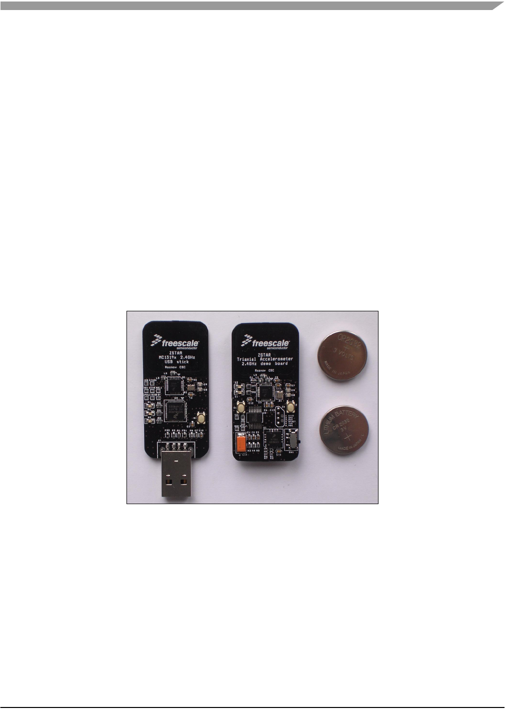
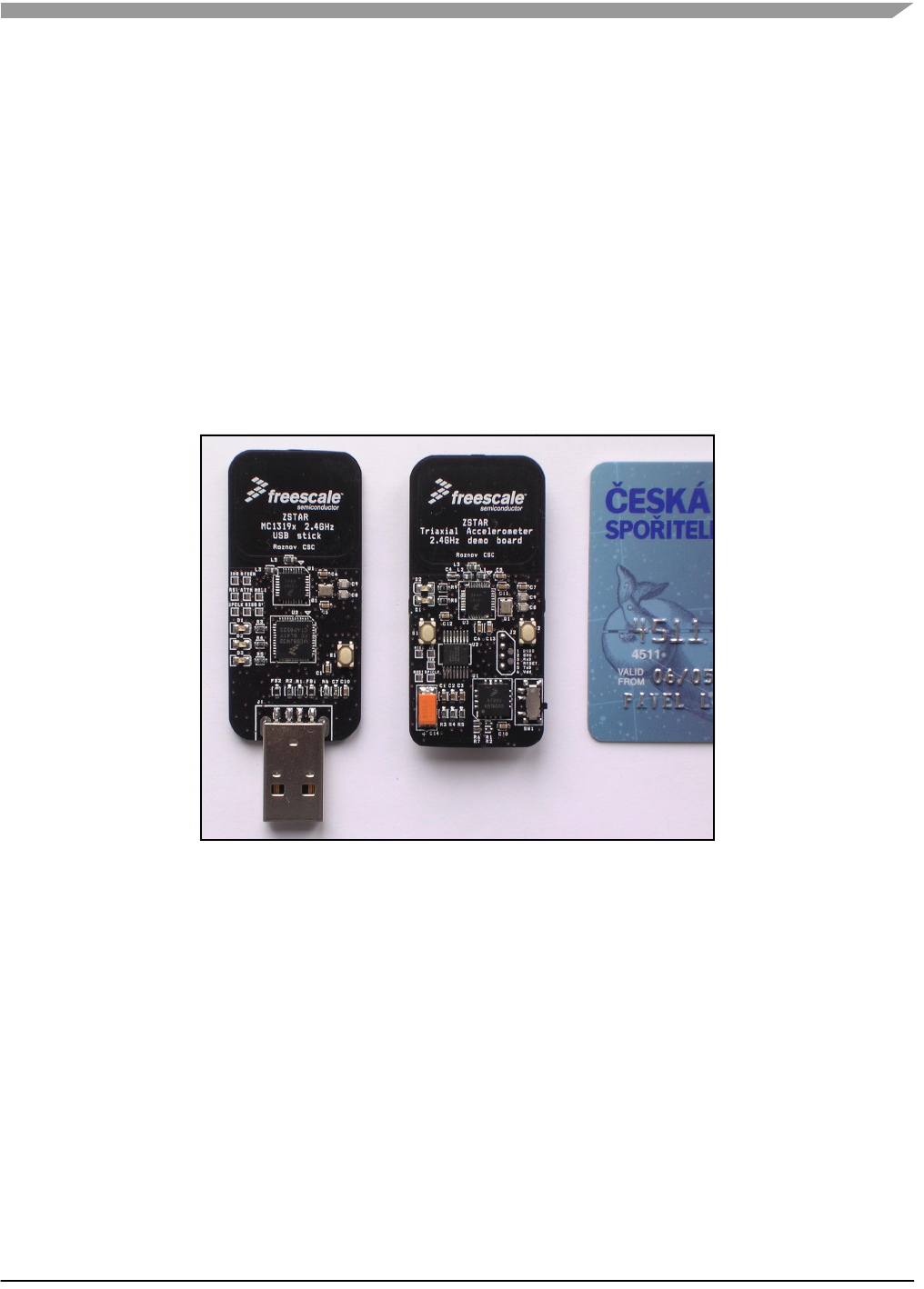
Figure 1-1 ZSTAR Demo photo (CR2032 batteries for comparison)
1.2 MMA7260Q 3-axis Accelerometer Sensor
The MMA7260Q low cost capacitive micromachined accelerometer features signal conditioning, a 1-pole
low pass filter and temperature compensation, and g-Select, which allows a selection from 4 sensitivities.
Zero-g offset full scale span and filter cut-offs are factory set and require no external devices. This device
includes a sleep mode making it ideal for handheld battery powered electronics.

Introduction
Wireless Sensing Triple Axis Reference design, Rev. 0.9
10 Freescale Semiconductor
Wireless Sensing Triple Axis Reference design, Rev. 0.9
Freescale Semiconductor 11
Chapter 2
Wireless Sensing Triple Axis Reference design introduction
2.1 Introduction
The Wireless Sensing Triple Axis Reference design (ZSTAR) has been designed as a wireless
complement to the previous STAR (Sensing Triple Axis Reference design) RD3112MMA7260Q demo. A
2.4GHz radio-frequency (RF) link based on the low-cost MC13191 family is used for connection from the
sensor to PC, allowing the visualization of key accelerometer applications.
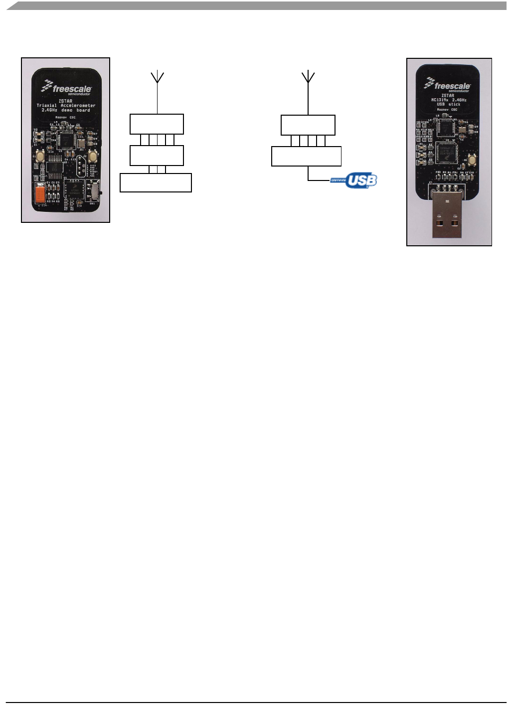
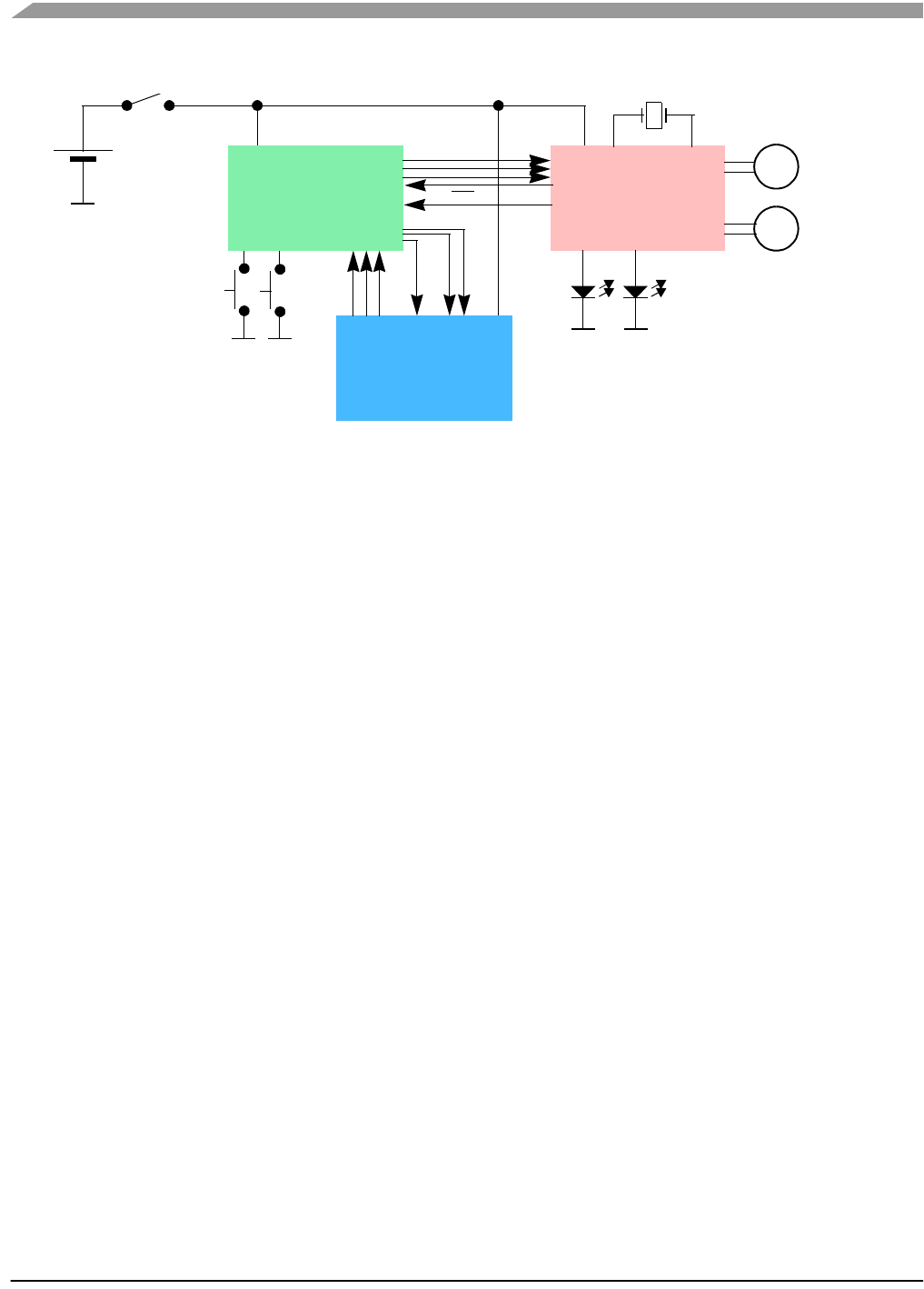
Figure 2-1ZSTAR demo overview
The demo consists of the two boards:
• Sensor Board (or remote board) containing the MMA7260Q 3-axis accelerometer, S08 family
MC9S08QG8 8-bit microcontroller and the 2.4GHz RF chip MC13191 for wireless communication.
• USB stick, again with the MC13191 RF front-end, and the HC08 family MCHC908JW32 for the
USB communication.
Both sides communicate over the RF medium utilizing the freely available software stack SMAC from
Freescale.
Wireless Sensing Triple Axis Reference design introduction
Wireless Sensing Triple Axis Reference design, Rev. 0.9
12 Freescale Semiconductor
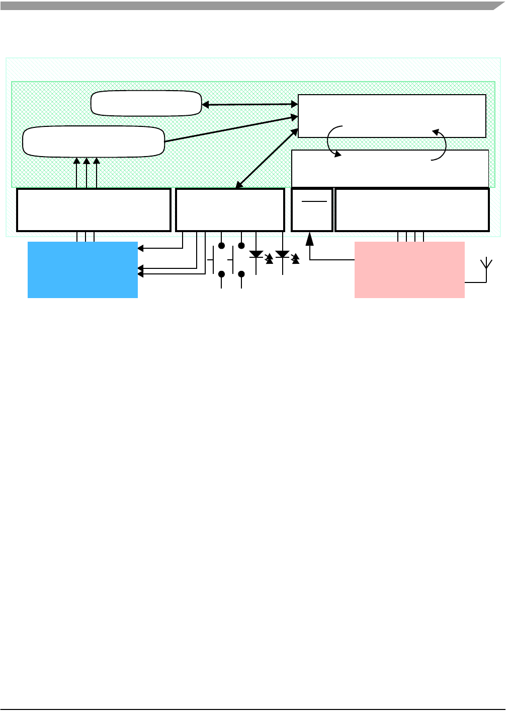
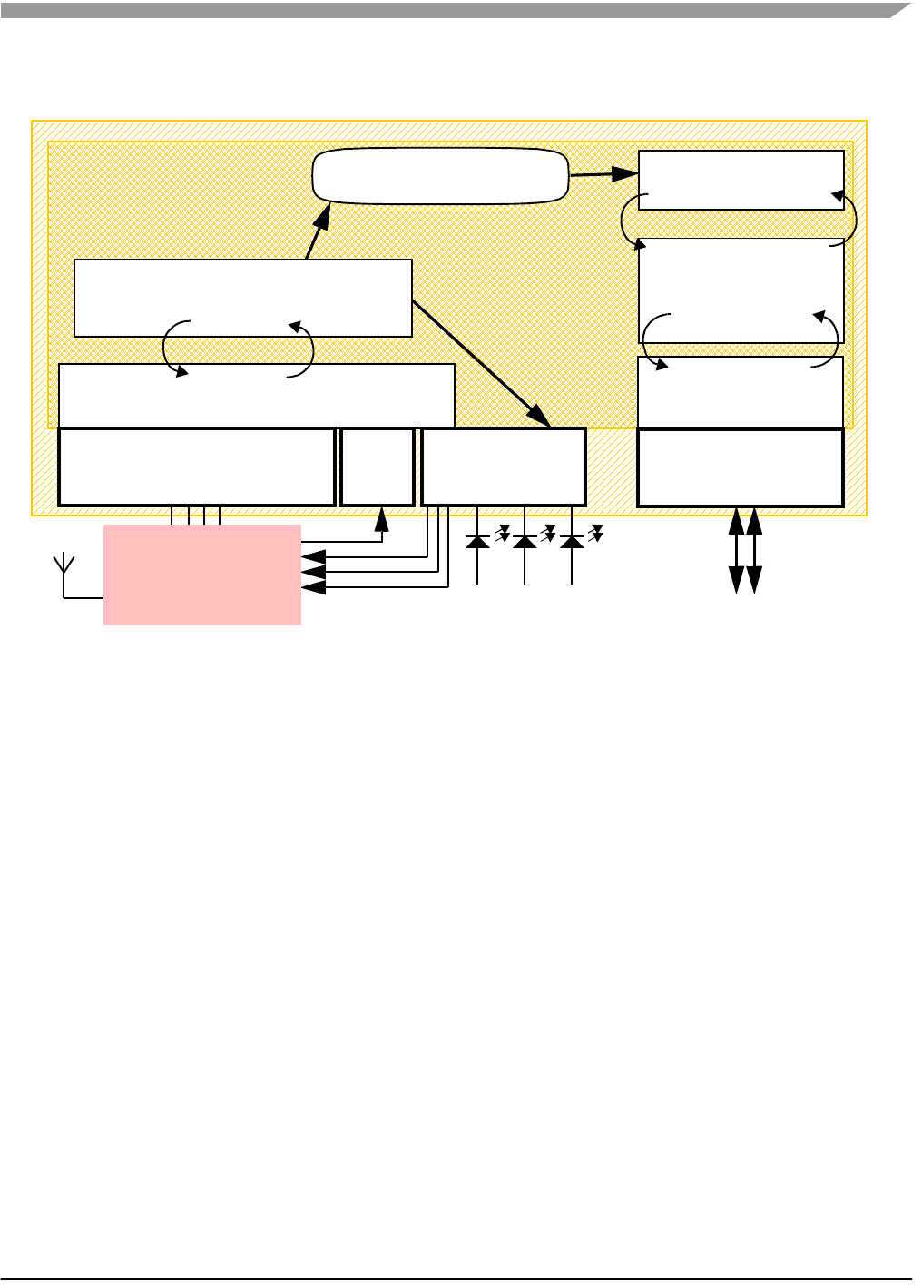
Figure 2-2ZSTAR Block diagram
2.2 Featured products
This demo consist of several Freescale products whose main features are listed below.
2.2.1 Triple Axis Accelerometer MMA7260Q
The ZSTAR board is a demonstration tool for the MMA7260Q, a 3-Axis Low-g accelerometer. The
MMA7260Q has many unique features that make it an ideal solution for many consumer applications,
such as freefall protection for laptops and MP3 players, tilt detection for e-compass compensation and
mobile phone scrolling, motion detection for handheld games and game controllers, position sensing for
g-mice, shock detection for warranty monitors, and vibration for out of balance detection.
Features such as low power, low current, and a sleep mode with a quick turn on time, allow the battery
life to be extended in end applications. The 3-axis sensing in a small QFN package requires only a 6mm
x 6mm board space, with a profile of 1.45mm, allowing for easy integration into many small handheld
electronics.
There are several other derivatives of the MMA7260Q:
•MMA7261Q with a selectable 2.5g to 10g range
•MMA6270Q is an XY dual axis accelerometer
•MMA6280Q is an XZ dual axis accelerometer
All members of this sensor family are footprint (QFN package) compatible which simplifies evaluation and
design of the target application.
2.2.2 Microcontroller MC9S08QG8
The MC9S08QG8 is a highly integrated member of Freescale’s 8-bit family of microcontrollers based on
the high-performance, low-power consumption HCS08 core. Integrating features normally found in larger,
more expensive components, the MC9S08QG8 MCU includes a background debugging system and
on-chip in-circuit emulation (ICE) with real-time bus capture, providing a single-wire debugging and
S08QG8
MC39
MMA7260Q
MC39
HC908JW32

Featured products
Wireless Sensing Triple Axis Reference design, Rev. 0.9
Freescale Semiconductor 13
emulation interface. It also features a programmable 16-bit timer/pulse-width modulation (PWM) module
(TPM), that is one of the most flexible and cost-effective of its kind.
The compact, tightly integrated MC9S08QG8 delivers a versatile combination, from wealth of Freescale
peripherals and the advanced features of the HCS08 core, including extended battery life with a
maximum performance down to 1.8V, industry-leading Flash and innovative development support. The
MC9S08QG8 is an excellent solution for power and size-sensitive applications, such as wireless
communications and handheld devices, small appliances, Simple Media Access Controller
(SMAC)-based applications and toys.
• MC9S08QG8 Features
– Up to 20 MHz operating frequencies at >2.1 volts and 16 MHz at <2.1 volts
– 8 K Flash and 512 bytes RAM
– Support for up to 32 interrupt/reset sources
– 8-bit modulo timer module with 8-bit prescaler
– Enhanced 8-channel, 10-bit analog-to-digital converter (ADC)
– Analog comparator module
– Three communication interfaces: SCI, SPI and IIC
2.2.3 MC13191 2.4 GHz ISM Band Low Power Transceiver
The MC13191 is a short range, low power, 2.4 GHz Industrial, Scientific, and Medical (ISM) band
transceivers. The MC13191 contains a complete packet data modem which is compliant with the IEEE®
802.15.4 Standard PHY (Physical) layer. This allows the development of proprietary point-to-point and
star networks based on the 802.15.4 packet structure and modulation format. For full 802.15.4
compliance, the MC13192 and Freescale 802.15.4 MAC software are required.
When combined with an appropriate microcontroller (MCU), the MC13191 provides a cost-effective
solution for short-range data links and networks. Interface with the MCU is accomplished using a four wire
serial peripheral interface (SPI) connection and an interrupt request output, which allows the use of a
variety of processors. The software and processor can be scaled to fit applications ranging from simple
point-to-point to star networks.
2.2.4 Microcontroller MCHC908JW32
The MCHC908JW32 is a member of the low-cost, high-performance M68HC08 Family of 8-bit
microcontroller units (MCU’s). All MCU’s in the family use the enhanced M68HC08 central processor unit
(CPU08) and are available in a variety of modules, memory sizes and types, and package types.
• MCHC908JW32 Features
– Maximum internal bus frequency: 8-MHz at 3.5-5V operating voltage
– Oscillators:
- 4-MHz crystal oscillator clock input with 32MHz internal phase-lock loop
- Internal 88-kHz RC oscillator for timebase wakeup
– 32,768 bytes user program FLASH memory with security feature
– 1,024 bytes of on-chip RAM
– 29 general-purpose input/output (I/O) ports:
– 8 keyboard interrupt with internal pull-up
- 3 pins with direct LED drive
- 2 pins with 10mA current drive for PS/2 connection

Wireless Sensing Triple Axis Reference design introduction
Wireless Sensing Triple Axis Reference design, Rev. 0.9
14 Freescale Semiconductor
– 16-bit, 2-channel timer interface module (TIM) with selectable input capture, output compare,
PWM capability on each channel, and external clock input option
– Timebase module
– PS/2 clock generator module
– Serial Peripheral Interface Module (SPI)
– Universal Serial Bus (USB) 2.0 Full Speed functions:
- 12 Mbps data rate
- Endpoint 0 with an 8-byte transmit buffer and an 8-byte receive buffer
- 64 bytes endpoint buffer to share amongst endpoints 1–4
Wireless Sensing Triple Axis Reference design, Rev. 0.9
Freescale Semiconductor 15
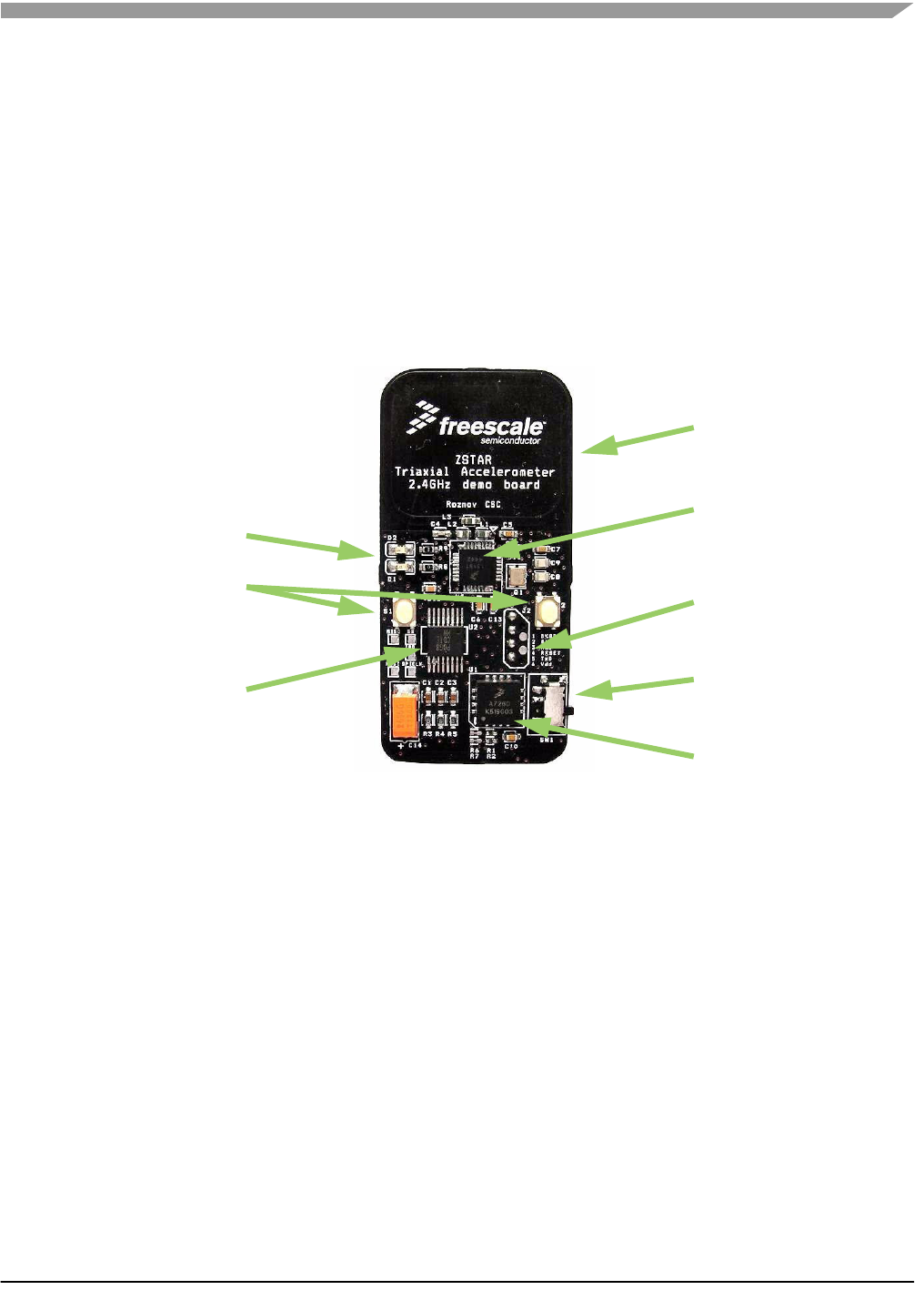
Chapter 3 Sensor Board description
3.1 Board overview
The Sensor Board utilizes a small footprint size dual-layer printed circuit board (PCB) containing all the
necessary circuitry for MMA7260Q accelerometer sensing and transferring data over a radio frequency
(RF).
Figure 3-1Sensor Board overview
The board is powered by a Lithium coin-sized CR2032 battery with provisions also made for the larger
capacity CR2477 size. The block diagram of the board is as follows:
Lithium battery on the opposite side
MC13191
MC9S08QG8
MMA7260Q
Battery Switch
LED indicators
PCB antennas
BDM interface
Buttons
Sensor Board description
Wireless Sensing Triple Axis Reference design, Rev. 0.9
16 Freescale Semiconductor
Figure 3-2Sensor board block diagram
Figure 3-3 shows in more detail, how different software and hardware modules co-operate with each
other. The main task of the Sensor board is to:
• periodically wake-up from power saving mode
• measure all three XYZ acceleration values from the sensor
• compose a data frame using simple ZSTAR RF protocol
• use SMAC (Simple Media Access Controller) to send this data frame over the RF link
• wait for an acknowledgment from the other end (here, the USB stick)
• go to sleep
This basic loop repeats roughly 20 times per second providing nearly a real-time response from the
sensor.
MMA7260Q
accelerometer
X Y Z sleep g-select
MC9S08QG8
MCU
MC13191
2.4GHz RF
receive antenna
transmit antenna
SPI
IRQ
CR2032 or CR2477
Lithium battery
A/D conversion of XYZ levels
Wireless Sensing Triple Axis Reference design, Rev. 0.9
Freescale Semiconductor 17
Figure 3-3ZSTAR Sensor board software overview
For the Sensor board operation, several of the MC9S08QG8’s hardware modules are used: Analog to
Digital Converter (ADC), Synchronous Peripheral Interface (SPI), External Interrupt Request module
(IRQ) and General Purpose Input/Output (GPIO).
3.2 A/D conversion of XYZ levels
The 3-axis accelerometer sensor MMA7260Q provides three separate analog levels for the X, Y and Z
axis. These outputs are ratiometric which means that the output offset voltage and sensitivity will scale
linearly with applied supply voltage. This is a key feature when interfacing to a microcontroller with A/D
converter reference levels tied to a power supply, because it provides system level cancellation of supply
induced errors in the analog to digital conversion process.
During the analog-to-digital conversion in the microcontroller, 8-bit resolution is used. MC9S08QG8 A/D
channels 0, 1 and 2 are connected to X (channel 1), Y (channel 2) and Z (channel 0) outputs of the
MMA7260Q. The microcontroller’s APCTL1 register enables these ADC channels for pin I/O control by
the ADC module.
The ADCCFG register controls the selected mode of operation, clock source, clock divide, and
configuration for low power or long sample time.
3.2.1 ADC module init:
APCTL1 = 0b00000111; /* 0,1,2 channels are ADC */
ADCCFG = 0b01100000; /* set prescale to 8, ADICLK=BUS, 8-bit, high speed */
Actual ADC measurements are done in the main software loop. There is a macro (called POWSUM) that
allows configuration of measurement to take several measurements of each channel during one loop. E.g.
changing POWSUM to 3, 2^3 = 8, each channel will be measured 8 times, with POWSUM 7, each channel
Sensor data
Analog-to-Digital converter
(ADC) module
MC9S08QG8
SMAC
ZSTAR RF protocol handler
sleep
software
calibration data
g-select
Serial Peripheral Interface
(SPI) module
IRQ
MC39
MMA7260Q
GPIO

Sensor Board description
Wireless Sensing Triple Axis Reference design, Rev. 0.9
18 Freescale Semiconductor
is measured 128 times. By default, POWSUM is 0, for 1 measurement of each channel. Before result values
are provided, the accumulated values are scaled back to the 8-bit range and inverted where necessary
(may be required depending on the physical MMA7260Q device orientation relative to the Earth gravity).
Raw (i.e. not calibrated) values are actually sent, the calibration and calculation of an exact g value is
done internally in the PC software.
3.2.2 ADC measurement
The following routine is used for accelerometer measurement:
unsigned int xx = 0;
unsigned int yy = 0;
unsigned int zz = 0;
unsigned char xxx, yyy, zzz;
#define POWSUM 0
for (i = 0; i < (1 << POWSUM); i++)
{
ADCSC1 = 0x01; //read X channel
while(!ADCSC1_COCO);
xx += ADCR;
ADCSC1 = 0x02; //read Y channel
while(!ADCSC1_COCO);
yy += ADCR;
ADCSC1 = 0x00; //read Z channel
while(!ADCSC1_COCO);
zz += ADCR;
}
xxx = ~(unsigned char)(xx >> POWSUM);
yyy = ~(unsigned char)(yy >> POWSUM);
zzz = (unsigned char)(zz >> POWSUM);
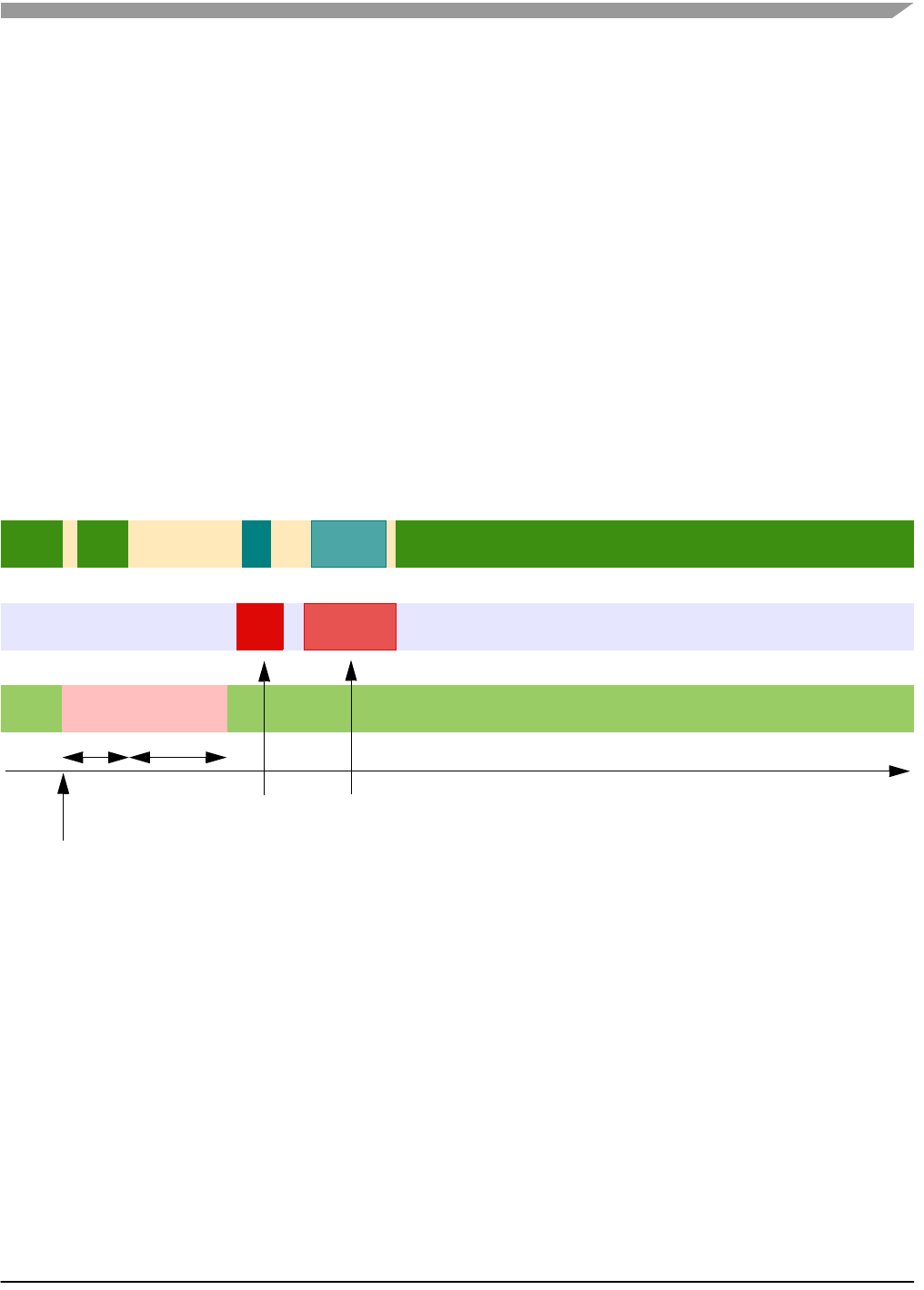
3.3 Power management
A CR2032 (or CR2477) Lithium battery provides a fairly limited charge for such a realtime-like demo that
demands frequent transmissions. Some sort of power management has to be implemented in order to
keep the current consumption at a reasonable level.
Typically, current consumptions of Sensor board components are as follows:
• 2.4GHz transceiver MC13191
– in Hibernate mode, 2.3µA
– in Doze mode, 35µA
– in Idle mode, 500µA
– in Transmit mode, 30mA
– in Receive mode, 37mA
Power management
Wireless Sensing Triple Axis Reference design, Rev. 0.9
Freescale Semiconductor 19
• 8-bit microcontroller MC9S08QG8
– in Stop mode, 750nA
– in Wait mode, 1mA
– in Run mode, 3.5mA
• low-g triaxial sensor MMA7260Q
– in Sleep mode, 3µA
– in Normal mode, 500µA
It is obvious that in a battery operated application care must be taken to ensure the lowest possible current
consumption, especially when the maximum current (provided by the battery) is somehow limited. A
CR2032 Lithium battery cannot provide current in the range of 40mA for long periods of time. To alleviate
high current surges, an additional large capacitor has been designed - see 3.4.10 Power supply.
For transmission and reception using the MC13191, a specific scheme has been used to ensure the
battery is not depleted or overloaded. Targeting a 20 samples per second (50ms period) transmission
rate, the following scheme for one transmission/sleep cycle is used for the data transfer:
Figure 3-4Transmission/sleep cycle details
As shown on the previous diagram, all parts of the Sensor board remain most of the time in
Sleep/Doze/Stop modes, in which the total current consumption is below 10µA.
During each loop, once the data has been acquired from sensor, transmission over the MC13191
transceiver is initiated. The current consumption of the transmitter is ~30mA at that time, but only for a
short period of time (typically ~600µs).
In order to keep the sensor board informed on the status of connection (for example, if the data-receiving
side - USB stick - is out of range, disconnected, etc.), the reception has to be turned on after the data has
been transmitted. This is not really required within each loop cycle, and in the actual implementation only
on every 8th loop the receive window opens (receiver is enabled to receive the acknowledgment). More
in the 5.3 ZSTAR RF protocol description.
time
Sleep
wake-up
Normal
MMA7260Q:
Doze
MC13191:
Stop
MC9S08QG8:
Stop
Sleep
Run Stop
Sensor
stabilizes Sensor
being
measured
TX
Wait
Wait
RX
optional
receive
window NOT TO SCALE
Doze
data
transmitted

Sensor Board description
Wireless Sensing Triple Axis Reference design, Rev. 0.9
20 Freescale Semiconductor
The reception window is larger to fit any incoming receive data and the current consumption is also higher
during reception, so this portion of current consumption would be one of the largest if the acknowledgment
was received in every loop cycle.
The “optional receive” feature allows huge power savings, still keeping the reception of acknowledgment
data from the data-receiving side.
Some further savings might be incorporated by utilizing the timer-triggered transceiver events that are
described in the MC13191 Reference Manual.The MC13191, for example, latches a so-called time-stamp
of each received frame. The data-receiving side may read this value and trigger the acknowledgment to
be sent at exactly specified time after reception (also, a start of data frame transmission can be
programmed as timer-triggered). The sensor board might then narrow its own receive window to perfectly
match the expected time of the acknowledgment frame. For the simplicity of code, this has not been
implemented in the current version of ZSTAR firmware.
3.3.1 MC13191 power management features
MC13191 provides several power saving modes. One of them is called Doze mode in which the
MC13191 crystal oscillator remains active. An internal timer comparator is functional too, providing a
power efficient and accurately timed way of waking-up the application after a specified time.
This feature is fully utilized within the Sensor board. The microcontroller calculates the time period for
which the application should be in power saving mode, then fills in the timer comparator registers in the
MC13191, and the microcontroller goes into Stop mode (MC13191 into Doze mode).
Once the timer reaches the pre-programmed time (a timer compare occurs), the MC13191’s IRQ signal
is asserted which brings the microcontroller out of the Stop mode. There are various scaling possibilities
that allow periods from a few µs up to 1073 seconds (~17 minutes) to be programmed, without
intervention of the microcontroller.
ZSTAR Sensor Board hardware overview
Wireless Sensing Triple Axis Reference design, Rev. 0.9
Freescale Semiconductor 21
3.4 ZSTAR Sensor Board hardware overview
This section describes the Sensor board in terms of the hardware design. The MC9S08QG8
microcontroller drives both the MMA7260Q sensor and the MC13191 RF transceiver.
3.4.1 Analog connections
The MMA7260Q sensor is connected to AD0, AD1, and AD2 inputs to analog-to-digital converter via RC
filters formed by R3, C3, R4, C2, R5, C1. These are recommended to minimize clock noise from the
switched capacitor filter circuit inside the sensor. Once the software filtering (also described in 3.2 A/D
conversion of XYZ levels) is employed, these RC filters may be completely omitted.
3.4.2 g-select connections
R1, R2, R6 and R7 components are made on the PCB. R1 and R2 are just footprints with no components
assembled, while R6 and R7 are connected with copper trace allowing the user to disconnect (cut) these
lines. By default, g-sel1 and g-sel2 MMA7260Q sensor input pins (used to select the acceleration range)
are connected to pins PTB0 and PTB1 of the microcontroller. The range can be controlled by software.
If user does not want to use this feature, the g-range can be selected by placing 0R resistors in the R1
and/or R2 positions. If no resistors are assembled, MMA7260Q internal pull-down resistors will
automatically select the 1.5g range (both g-sel inputs low).
Once R6 and R7 are cut, PTB0 and PTB1 (or their alternate SCI functionality of RxD1 and TxD1, or KBI
or AD inputs) may be used. These signals are also routed to BDM connector, pins 3 and 5.
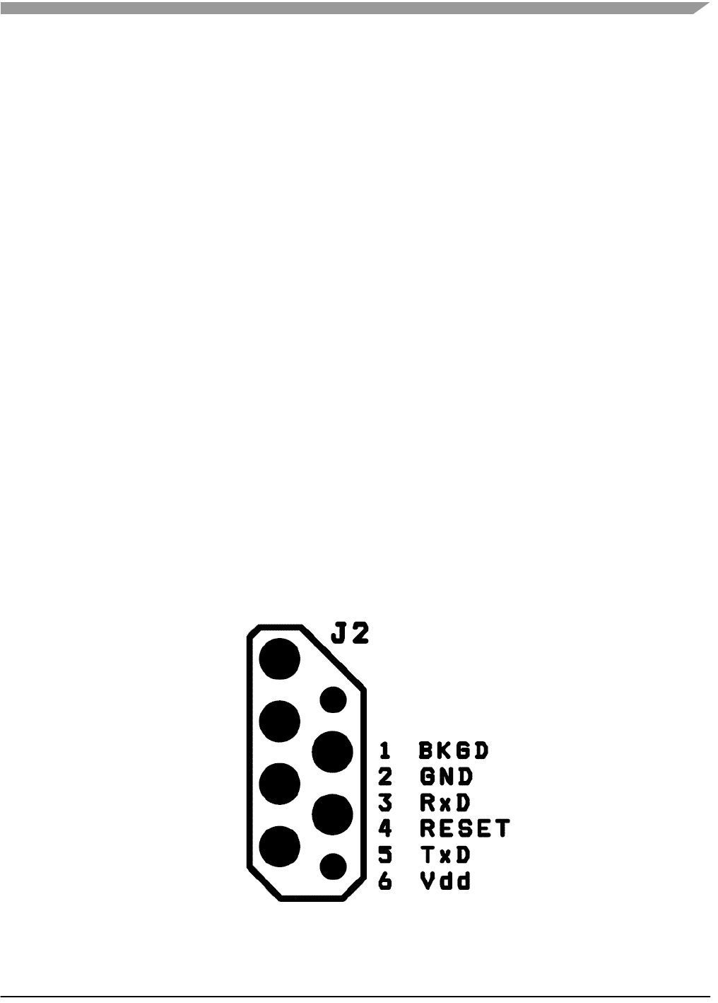
3.4.3 BDM (Background Debug Mode) connections
A J2 connector is a non-standard footprint primarily intended for in-factory programming and testing via
“spring-needle” type of connections. The J2 connector carries all standard signals for Background Debug
Mode communication so if required, one may solder wires and a standard 2x3 pins 2.54mm (100mil) pitch
header for regular BDM re-programming. The pin numbering is shown on Figure 3-5.
Figure 3-5BDM connector layout
1
23
45
6
Wireless Sensing Triple Axis Reference design, Rev. 0.9
22 Freescale Semiconductor
Sensor Board description
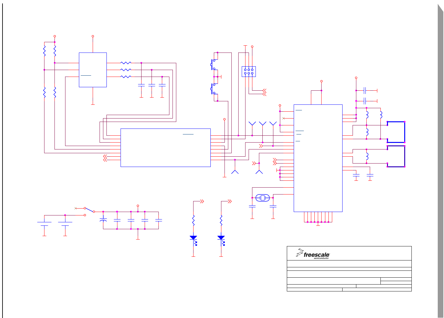
3.4.4 Sensor Board schematics
Figure 3-6Sensor board schematics
G_SEL2/TxD
G_SEL1/RxD
VDD
VDD
VDD
VDD
VDD
VDDA
GND GND
GND
GND GND
GND
GND
GND
GND
GND GND GND GND
GND
GNDGND
VDD
VDD
GND GND
GND
GND
MOSI
SPICLK
MOSI
G_SEL1/RxD
G_SEL2/TxD
LED1
LED2
LED1 LED2
SPICLK
Title
Size
Design Name:
Rev
Modify Date: Sheet of
Schematic Name:
Copyright Freescale
POPI Status:
Author:
1.0
Low-cost 2.4GHz Triax Board
Freescale Semiconductor RCSC
1. maje 1009
756 61 Roznov p.R., Czech Republic, Europe
A4
1 1
Monday, January 30, 2006
SCHEMATIC1
General Business Information
Radomir Kozub & Pavel Lajsner
2005
X:\ICONN\IC108 - LOW-COST 2.4GHZ AND XYZ ACCELEROMETER DEMO\HW\00239\00239.DSN
12
Q1
16MHz NX2520SA
Q1
16MHz NX2520SA
R2
INF
R2
INF
1
SSSS
R3 10kR3 10k
C11
10nF
C11
10nF
C12
10nF
C12
10nF
R1
INF
R1
INF
R5 10kR5 10k
BATT1
Battery/Renata CR2032
BATT1
Battery/Renata CR2032
1 2
3 4
65
J2
BDM
J2
BDM
RFIN- 1
RFIN+ 2
PAO+ 5
PAO- 6
GPIO4
8GPIO3
9GPIO2
10 GPIO1
11
RST
12
RXTXEN
13
ATTN
14
CLKO
15
SPICLK
16
MOSI
17
MISO
18
CE
19
IRQ
20
VDDD 21
VDDINT 22
GPIO5
23
GPIO6
24
GPIO7
25
CRYSTAL1
26
CRYSTAL2
27
VDDLO2 28
VDDLO1 29
VDDVCO 30
VBATT 31
VDDA 32
EPGND
36 EPGND
37 EPGND
38 EPGND
39 EPGND
40 EPGND
41
EPGND
35
EPGND
34
EPGND
33
U3 MC13191FCU3 MC13191FC
C6
10nF
C6
10nF
C7
10nF
C7
10nF
D2
LED
D2
LED
L2
22nH
L2
22nH
1
SPICLKSPICLK
g-Sel1
1
g-Sel2
2
VDD 3
VSS
4
SLEEP
12 Z13
Y14
X15
U1 MMA7260Q
U1 MMA7260Q
L3
5.6nH
L3
5.6nH
C1
100nF
C1
100nF
C5 10nFC5 10nF
L1
22nH
L1
22nH
D1
LED
D1
LED
BATT2
Battery/Renata CR2477
BATT2
Battery/Renata CR2477
1
IRQIRQ
1 3
42
S1
Alps SKRP
S1
Alps SKRP
L4
4.7nH
L4
4.7nH
1
MOSIMOSI
R7
0R
R7
0R
1
MISOMISO
+
C14
470uF/4V
+
C14
470uF/4V
R9
0R
R9
0R
C13
10nF
C13
10nF
R6
0R
R6
0R
C9
6.8pF
C9
6.8pF
C3
100nF
C3
100nF
13
4 2
S2
Alps SKRP
S2
Alps SKRP
R8
0R
R8
0R
PTB4/MISO1 8
PTB3/KBI7/AD7/MOSI1
9
PTA4/BKGD/MS/ACMP1O 2
Vdd 3
PTA0/KBI0/AD0/TPM1CH0/ACMP1+
16
PTA1/KBI1/AD1/ACMP1-
15
PTA2/KBI2/AD2/SDA1
14
PTA5/RESET/IRQ/TCLK 1
Vss 4
PTB7/SCL1/EXTAL 5
PTB6/SDA1/XTAL 6
PTB5/TPM1CH1/SS1 7
PTB1/KBI5/AD5/TxD1
11 PTB0/KBI4/AD4/RxD1
12 PTA3/KBI3/AD3/SCL1
13
PTB2/KBI6/AD6/SPSCK1
10
U2
MC9S08QG8CDTE
U2
MC9S08QG8CDTE
C8
6.8pF
C8
6.8pF
C2
100nF
C2
100nF
C10
10nF
C10
10nF
SW1
Alps/SSSS811101
SW1
Alps/SSSS811101
R4 10kR4 10k
C4 100pFC4 100pF

ZSTAR Sensor Board hardware overview
Wireless Sensing Triple Axis Reference design, Rev. 0.9
Freescale Semiconductor 23
3.4.5 Button connections
Two buttons (S1 and S2) are connected directly to pins PTB6 and PTB7. Both have internal pull-up
resistors, but are not part of the Keyboard interrupt module, therefore don’t allow a direct microcontroller
wake-up from the Stop modes.
3.4.6 MC13191 to MC9S08QG8 microcontroller interface
In order to fit all the necessary circuitry onto a 16-pin microcontroller, the full recommended MC13191
interface has had to be reduced. The full interface includes the following connections:
• 4-wire Synchronous Peripheral Interface (SPI) connection (MISO, MOSI, SPICLK, CE)
• Interrupt Request signal (IRQ)
• Attention (ATTN) wake-up signal
• Receive/Transmit Enable (RXTXEN) signal
• External Reset (RST) signal
SPI and IRQ are vital for the communication and configuration ofthe MC13191. SPI is connected to the
MC9S08QG8 SPI module (pins PTB4/MISO1, PTB3/MOSI1, PTB2/SPSCK1, and GPIO pin PTB5 for
CE).
Interrupt Request (IRQ) is connected to the microcontroller IRQ pin sharing its alternate RESET function
when BDM communication is active.
Attention (ATTN)signal is intended to externally wake-up the MC13191 from Doze and Hibernate
modes. Since this feature is not used and exit from the Doze mode is done using a timer compare event,
The ATTN pin is not routed to the microcontroller and needs to be connected to Vdd.
Receive/Transmit Enable (RXTXEN) signal is used to control transitions to/from receive and transmit
modes. Since this can be accomplished just by software programming and/or timer compare events, this
connection to the microcontroller may also be omitted, saving an additional pin. RXTXEN is connected to
Vdd.
External Reset (RST) signal places the transceiver in a complete reset condition (Off mode and power
down). Alternative Software reset is also possible and since Off mode (the one with the lowest possible
power consumption) is not required too, RST is connected to Vdd too.
3.4.7 MC13191 RF interface
The RF interface (antennas) were designed with the cost and board size in mind. Among several designs,
the PCB layout antennas were in the main consideration (cost). Of several PCB antenna designs
available for the 2.4GHz band (F-antenna, dipole, loop), the loop antenna has been selected mainly
because of the size required on the PCB.
The MC13191 transceiver is designed with separated RF IN (receive) and PA OUT (transmit) paths. To
avoid the need for an antenna switch, two separate antennas need to be used. Both ZSTAR boards (USB
stick and Sensor Board) use the same antenna layout, there are two antennas on the PCB, just on the
opposite sides of the PCB.
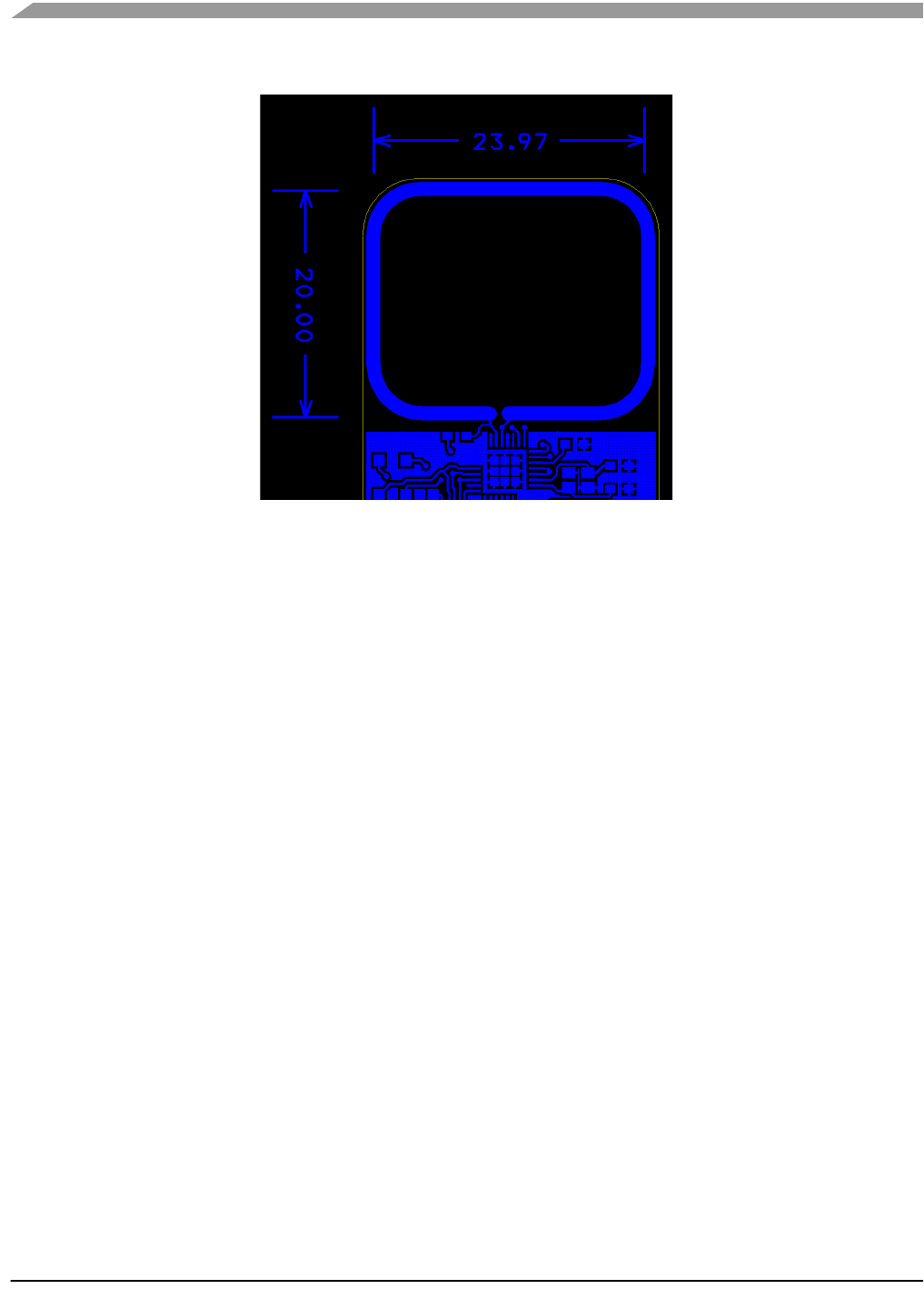
The antenna is designed as a rectangle, 20x24mm (780x940mils), made of 1.25mm (50mils) wide trace
of copper. The corners are rounded with a 3.8mm (150mils) radius.
Sensor Board description
Wireless Sensing Triple Axis Reference design, Rev. 0.9
24 Freescale Semiconductor
Figure 3-7ZSTAR antenna layout
The matching is provided by L3 (transmit antenna) and L4 (receive antenna) coils. L1 and L2 coils bias
the transmitter output transistors to the VDDA level.
The inductors used in this design are from TDK:
L3 (5.6nH) MLG1608B5N6DT
L4 (4.7nH) MLG1608B4N7ST
and L1, L2 (22nH) MLG1608B22NJT.
3.4.8 Clocking options of MC9S08QG8
Due to the availability of accurate timing provided by the MC13191 transceiver, an internal oscillator (ICG)
in the MC9S08QG8 is used as the main clock source for the microcontroller. The protocol related timing
is derived from MC13191 timers, the microcontroller itself is clocked from an internal oscillator, leaving
the oscillator pins as GPIO. This is highly beneficial to the limited pin count microcontroller.
3.4.9 LED indicators connections
The MC13191 allows extension to the number of general I/O pins by 7 additional GPIO connections. Two
of these (GPIO1 and GPIO2) are used for LED indicators. R8 and R9 are their current limiting resistors,
and in the actual design orange LED’s are used, with a threshold voltage around 2.0-2.5V.
The remaining unused GPIO3-GPIO7 signals are connected to ground, improving the physical PCB
layout of the MC13191.

ZSTAR Sensor Board hardware overview
Wireless Sensing Triple Axis Reference design, Rev. 0.9
Freescale Semiconductor 25
3.4.10 Power supply
The Sensor board is powered by a Lithium coin-sized battery. The primary choice was the popular
CR2032, with a PCB layout provision made for the CR2477 size. This bigger battery holds roughly 4 times
more charge (~1000mAh), but it is not as popular as CR2032 size.
A surface mounted SMTU series battery holder from RenataTM is placed on the underside of the PCB.
The SMTU series holders provide (by mechanical construction) battery reverse protection, so no
additional circuitry is required. Slide switch SW1 disconnects the battery from the application when not in
use.
A large tantalum capacitor (C14, 470µF/4V) improves the response of the power supply to current peaks
caused by reception or transmission. Coin-sized Lithium CR2032 batteries are targetted at a maximum
continuous discharge current in the range of 3mA. Such a large capacitor helps to supply enough current
to the MC13191 during a receive/transmit without significant Vdd voltage drops.

Sensor Board description
Wireless Sensing Triple Axis Reference design, Rev. 0.9
26 Freescale Semiconductor
3.5 Bill of Materials
Table 3-1. Sensor board bill of materials
Item Quantity Reference Part Manufacturer Manufacturer order code
1 1 BATT1 battery holder
CR2032 Renata SMTU 2032-1
2 3 C1,C2,C3 100nF TDK C1608JB1H104K
3 1 C4 100pF TDK C1608CH1H101J
4 7 C5,C6,C7,C10,
C11,C12,C13 10nF TDK C1608CH1E103J
5 2 C8,C9 6.8pF TDK C1608CH1H070D
6 1 L3 5.6nH TDK MLG1608B5N6DT
7 1 L4 4.7nH TDK MLG1608B4N7ST
8 2 D1,D2 Kingbright
KP-1608SEC Kingbright KP-1608SEC
9 1 J2 BDM + serial N/A
10 2 L1,L2 22nH TDK MLG1608B22NJT
11 1 Q1 16MHz NX2520SA NDK NX2520SA 16MHz EXS00A-02940
Specification n° EXS10B-07228
12 2 R1,R2 N/A N/A
13 3 R3,R4,R5 10k resistor 0603
package
14 2 R6,R7 N/A N/A
15 2 R8,R9 0R resistor 0603
package
16 1 SW1 slide switch
Alps/SSSS811101 Alps SSSS811101
(or SKRPACE010 or SKRPABE010)
17 2 S1,S2 switch SKRP Alps SKRPADE010
(or SKRPACE010 or SKRPABE010)
18 1 U1 MMA7260Q Freescale MMA7260Q
(MMA7260QR2 for tape and reel)
19 1 U2 MC9S08QG8CDTE Freescale MC9S08QG8CDTE
20 1 U3 MC13191FC Freescale MC13191FC
(MC13191FCR2 for tape and reel)
21 1 C14 470uF/4V Vishay 594D477X9004C2T
Wireless Sensing Triple Axis Reference design, Rev. 0.9
Freescale Semiconductor 27
Chapter 4 USB stick board description
4.1 Board overview
The USB stick board utilizes the same small footprint as Sensor Board is also a dual-layer printed circuit
board (PCB). It contains the minimalistic design of the MC13191 RF transceiver connected through an
8-bit MCHC908JW32 microcontroller to the USB. It’s main task is to receive data from the Sensor Board
and transfer it to the PC over the USB link.
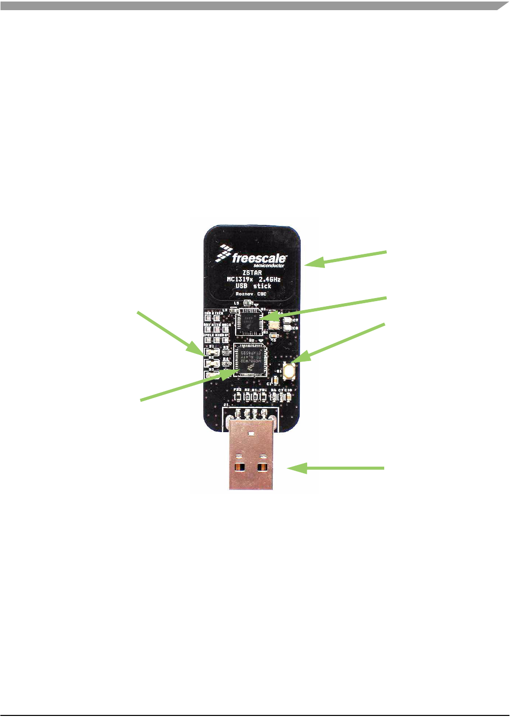
Figure 4-1USB stick board overview
The USB stick board is powered from the USB. The block diagram of the board is as follows:
MC13191
MCHC908JW32
LED indicators
PCB antennas
USB “A” type plug
Button
USB stick board description
Wireless Sensing Triple Axis Reference design, Rev. 0.9
28 Freescale Semiconductor
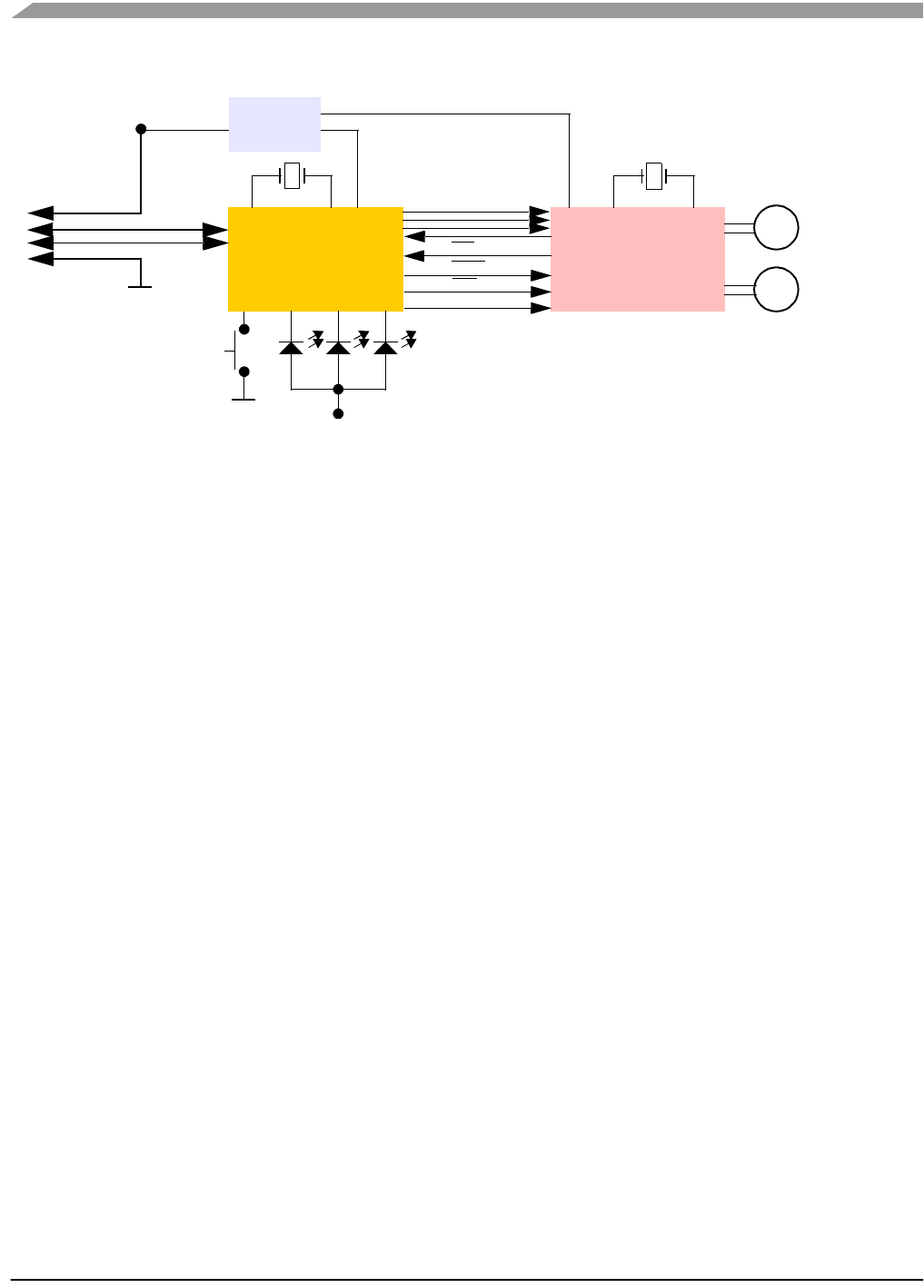
Figure 4-2USB stick board block diagram
Figure 4-3 shows, in more detail, how different software and hardware modules co-operate with each
other. There are two main tasks of the USB stick board:
• receive the data from the MC13191 transceiver and store it in RAM buffer
• handle the USB module communication, decode and provide the data from the RAM buffer
These two are somewhat independent and the only common point between them is the accelerometer
and button data buffer in RAM. The RF software communicates with the Sensor Board and retrieves the
latest accelerometer data. This is stored in RAM and can be independently read by the PC application via
the USB link. The protocol employed on the PC side is just a subset of the simple STAR protocol used in
the original RD3112MMA7260Q demo. The protocol is described in chapter 5.4 STAR protocol and
ZSTAR extensions (over USB).
MCHC908JW32
MCU
MC13191
2.4GHz RF
receive antenna
transmit antenna
SPI
IRQ
ATTN
RST
RXTXEN
USB
+5V USB voltage
regulators
+5V USB
Board overview
Wireless Sensing Triple Axis Reference design, Rev. 0.9
Freescale Semiconductor 29
Figure 4-3ZSTAR USB stick board software overview
For the USB stick board operation, several MCHC908JW32 hardware modules are used: USB 2.0
Full-speed module (USB), Synchronous Peripheral Interface (SPI), Keyboard Interrupt module (KBI) and
a General Purpose Input/Output (GPIO).
SMAC
low-level USB
Sensor & Button data
USB connection to PC
USB protocol
ZSTAR RF protocol handler
MCHC908JW32
USB 2.0
“virtual serial port”
software
Serial Peripheral Interface
(SPI) module KBI GPIO Full Speed module
MC39
protocol driver
or mouse
handler
simple STAR
protocol handler

USB stick board description
Wireless Sensing Triple Axis Reference design, Rev. 0.9
30 Freescale Semiconductor
4.2 ZSTAR USB stick Board hardware overview
This section describes the USB stick board in terms of the hardware design. The MCHC908JW32
microcontroller drives the MC13191 RF transceiver and communicates over USB with PC.
4.2.1 USB connections
Two USB communication lines are connected directly via R1 to PTE2/D+ and R2 to PTE3/D-
microcontroller pins. There, the R1 and R2 resistors define the output impedance of both drivers (ZDRV
as per chapter 7 of the USB 2.0 specifications).
Terminating the D+ line with a 1.5kΩ pull-up resistor (required for Full-speed signalling) is internal in the
MCHC908JW32.
A USB “A” type SMT Plug is designed at the edge of the USB stick board allowing the stick to be
connected directly into a USB hub without the need for a cable.
4.2.2 Power supply
The USB stick board is a Low-power Bus-powered Function (as defined in chapter 7.2.1.3 of USB 2.0
specifications). This means that a maximum of one unit load (100mA) may be drawn by the USB Stick
board. Ferrite beads are included on the VBUS and GND USB connections to minimize EMI. The
recommended type is a GLF1608T100M or similar from TDK.
VBUS voltage is defined as a minimum 4.4V and a maximum 5.25V on a Low-power Bus-powered
Function.
The MC13191 RF transceiver requires a maximum power supply voltage of 3.4V and the MCHC908JW32
microcontroller could not guarantee an internal 3.3V regulator working at such a low power supply.
Therefore, two separate voltage regulators need to be implemented, and in addition, the voltage levels
have to be close enough to avoid the need for level shifters (for the MC13191 to MCHC908JW32
microcontroller interface).
4.2.2.1 Fixed voltage regulators
Two voltage levels (3.3V for MC13191 and 3.6V for MCHC908JW32) were selected. For these levels, a
low-cost, small footprint fixed regulator exists. The NCP502/A series regulators from ON
SemiconductorTM were successfully implemented.
The NCP502/A series voltage regulator is an 80mA CMOS fixed linear regulator designed primarily for
handheld communication equipment and portable battery powered applications which require a low
quiescent current.
Each device contains a voltage reference unit, an error amplifier, a PMOS power transistor, resistors for
setting the output voltage, current limit, and temperature limit protection circuits. The NCP502/A has been
designed to be used with low cost ceramic capacitors. The device is housed in a micro-miniature SC70-5
surface mount package. Standard voltage versions are 1.5 V, 1.8 V, 2.5 V, 2.7 V, 2.8 V, 3.0 V, 3.3 V, 3.5
V, 3.6 V and 5.0 V. Other voltages are available in 100 mV steps.
Typically, a low-cost 1µF ceramic capacitor is recommended for input and output decoupling. 0603-sized
SMD TDK capacitor C1608X5R1A105K was used.

ZSTAR USB stick Board hardware overview
Wireless Sensing Triple Axis Reference design, Rev. 0.9
Freescale Semiconductor 31
Enable Operation - Enable pin of 3.3V regulator (for MC13191) is connected to PTC3 pin of the
microcontroller. This way, the microcontroller may completely turn off the RF part of the application to
minimize power consumption in USB suspend modes.
Alternatively, power down of the MC13191 RF transceiver may be done by forcing it into Off mode by
pulling the RST pin low.
4.2.3 MC13191 to MCHC908JW32 microcontroller interface
On the USB stick board the full recommended MC13191 interface has been used. This includes the
following connections:
• 4-wire Synchronous Peripheral Interface (SPI) connection (MISO, MOSI, SPICLK, CE)
• Interrupt Request signal (IRQ)
• Attention (ATTN) wake-up signal
• Receive/Transmit Enable (RXTXEN) signal
• External Reset (RST) signal
The SPI connection is connected to the MCHC908JW32 SPI module signals (MISO, MOSI, SPCLK, SS).
The IRQ signal is routed to the PTA3/KBA3 Keyboard interrupt module pin instead of the MCHC908JW32
IRQ pin, which is left for the MON08 interface and the Button connection. The reason for re-routing this
signal is that VTST (1.5xVDD, up to 8V) is applied to the microcontroller’s IRQ during programming,
therefore some additional jumper configuration would be required to disconnect this voltage fromthe
MC13191. Here, the IRQ‘s MON08 function is only shared with the button under the condition that the
button is not pressed during programming.
The remaining three signals (ATTN, RXTXEN and RST) are connected to GPIO signals of port D (PTD0,
PTD2 and PTD1).
4.2.4 Oscillator and clocking options
The MCHC908JW32 microcontroller requires a stable clock, mainly for the Full-speed USB module
operations. USB specifications define an overall 2500ppm (0.25%) accuracy. Basically, any generic
4MHz crystal is sufficient for such accuracy. The main issue with 4MHz crystals are their physical size.
Due to the nature of crystal resonating elements, the 4MHz crystals are simply far too big for the USB
stick in the ZSTAR demo.
Another option is a SAW resonator (e.g. CERALOCKTM series from Murata). These are usually sorted
and selected by the manufacturer to fit the USB 2.0 Full-speed accuracy required. Today, only 6, 12, 24
and 48MHz versions are available from Murata. A 6MHz version (manufacturer order code
CSTCR6M00G15) has been used in the USB stick design, although the 6MHz frequency is outside the
MCHC908JW32 microcontroller specifications.
Provision is also made on the PCB (Q3 component) for an Epson SG-310 series (or compatible) Crystal
Oscillator (active output). Here, a 4MHz version oscillator is contained in a small 3.2x2.5mm package.
4.2.5 LED indicators connections
The MCHC908JW32 microcontroller allows a direct drive of LED’s on its three pins. PTB0, PTB1 and
PTB5 are high-current open-drain outputs, so the LED’s D1, D2 and D3 are connected to these
high-current outputs.

USB stick board description
Wireless Sensing Triple Axis Reference design, Rev. 0.9
32 Freescale Semiconductor
4.2.6 Button connection
One button is implemented on the USB stick board. It is connected to the IRQ microcontroller pin that has
internal pull-up and allows an easy software interrupt.
4.2.7 MON08 interface
For MCHC908JW32 in-circuit programming, a MON08 interface is required. Several pins must be
connected to specific voltage levels in order for the MCHC908JW32 to enter the Monitor mode. The
details are described in the MCHC908JW32 datasheet, Chapter 7 Monitor ROM (MON).
To minimize the number of MON08 connections, several pins are hardwired to specific voltage levels
directly on the USB stick board. Namely, PTA1 to Vdd, PTA2 and PTC1 to GND.
Pins PTA0, RST, IRQ and OSC1, together with the power supply lines, are routed to PCB pads MON08
connector (J3).
There is no standard physical connector to be soldered onto the J3 footprint. The J3 connector pads are
used during manufacturing for the initial in-circuit programming. Further re-programming of the USB stick
maybe done using an AN2295 Bootloader as described in chapter 5.5.
4.2.8 Optional serial interface
For the purpose of evaluating the USB functions of the MCHC908JW32 microcontroller, a few other pins
were routed to an additional PCB pads connector (J2). The two TIM timer pins are connected to J2
allowing emulation of SCI, IIC or such like serial interfaces in software. A simple example of a USB to
UART converter software is a part of the AN3153 Application note - Using the Full-Speed USB Module
on the MCHC908JW32.