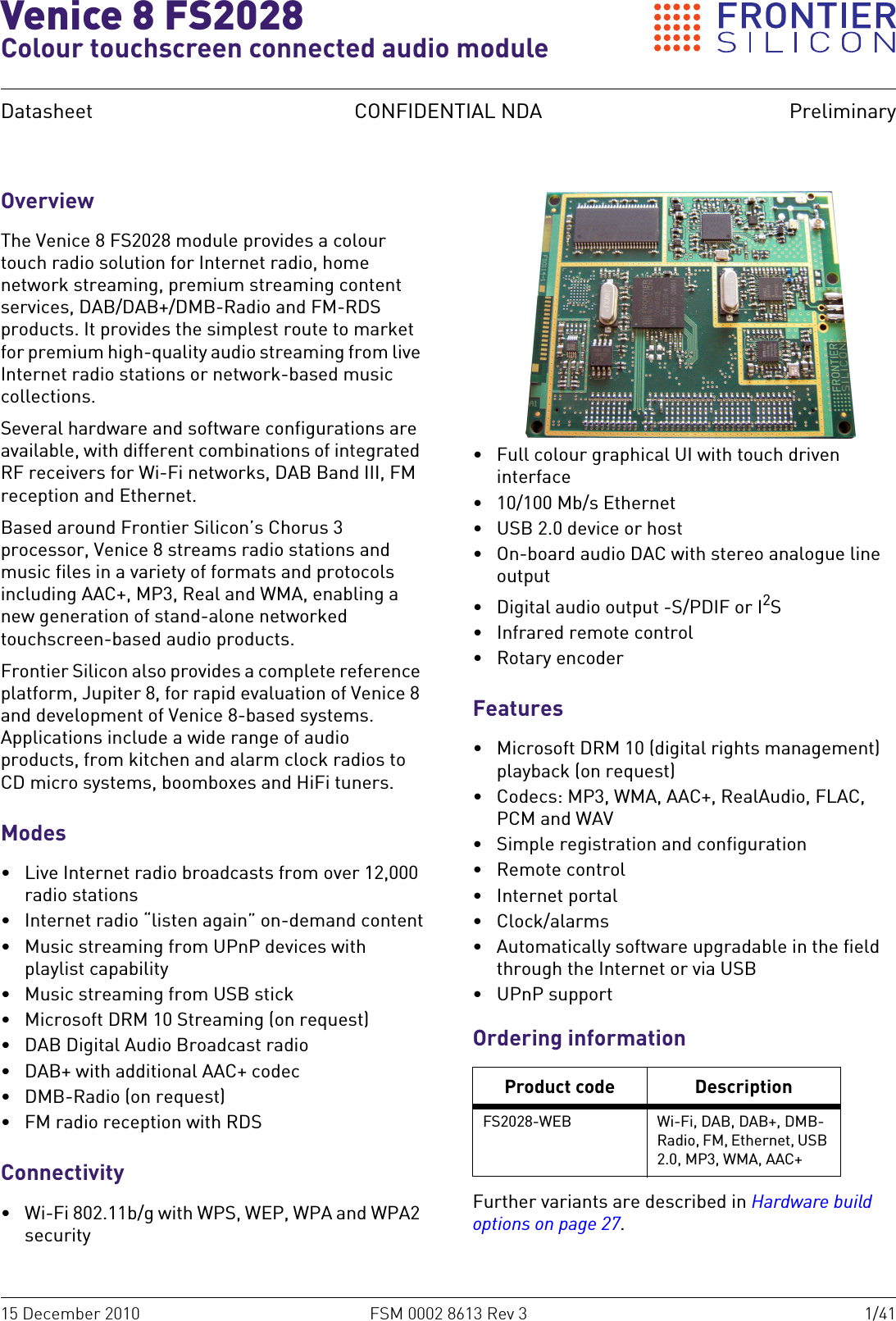
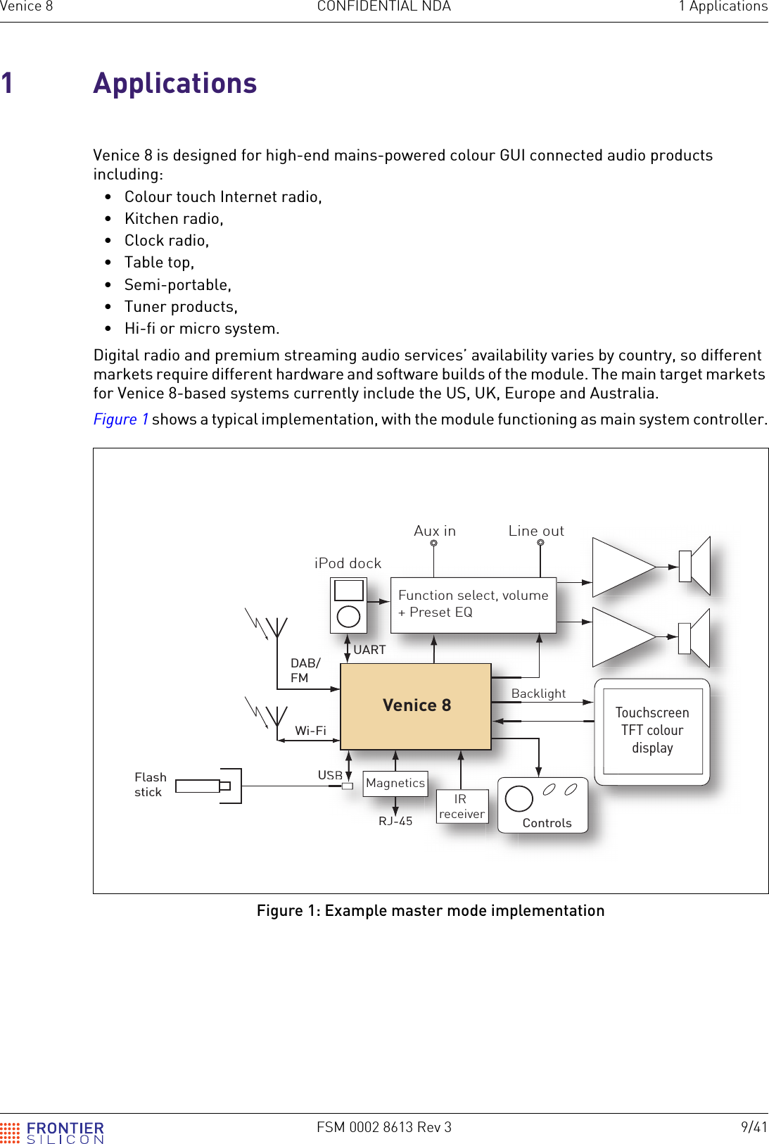
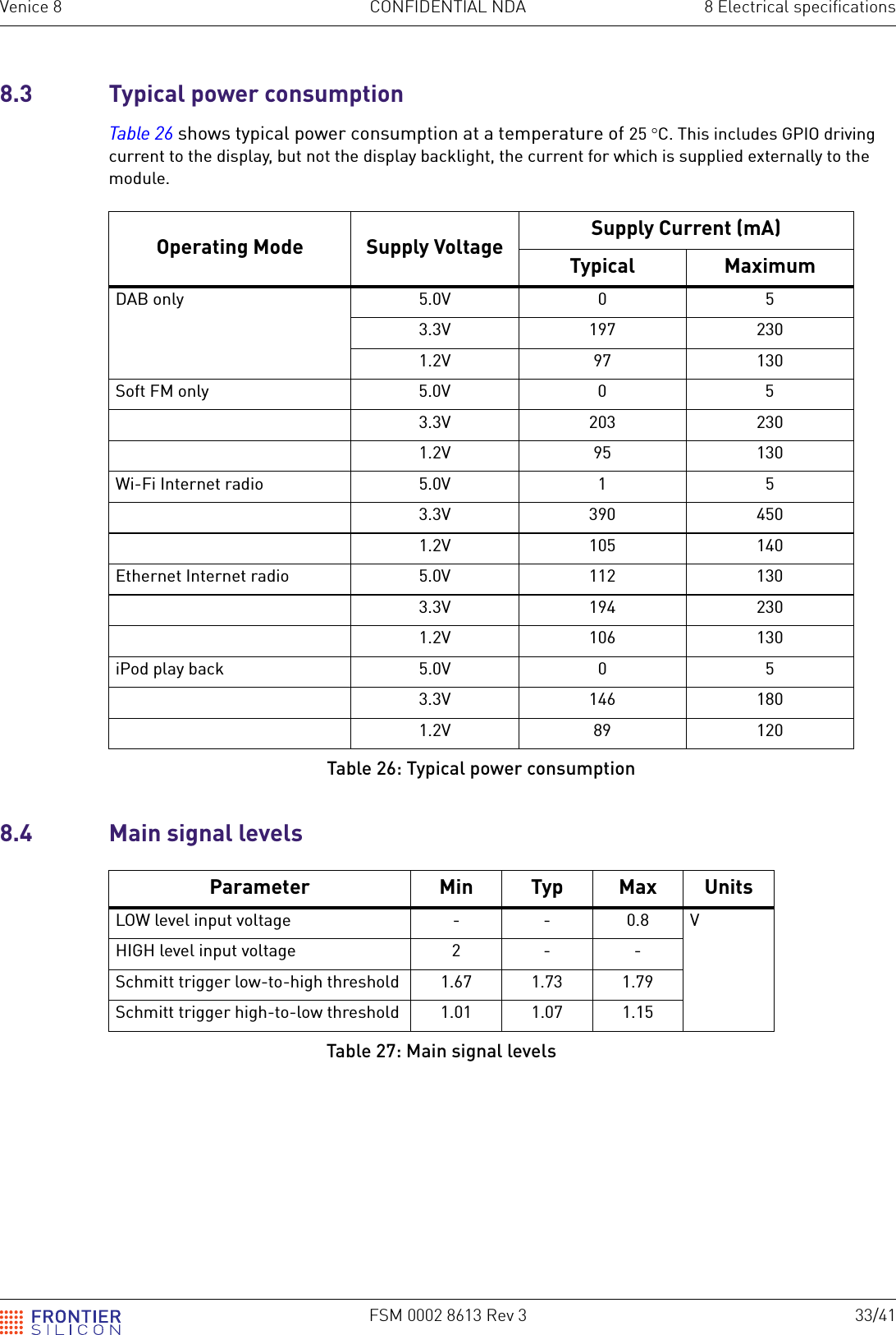
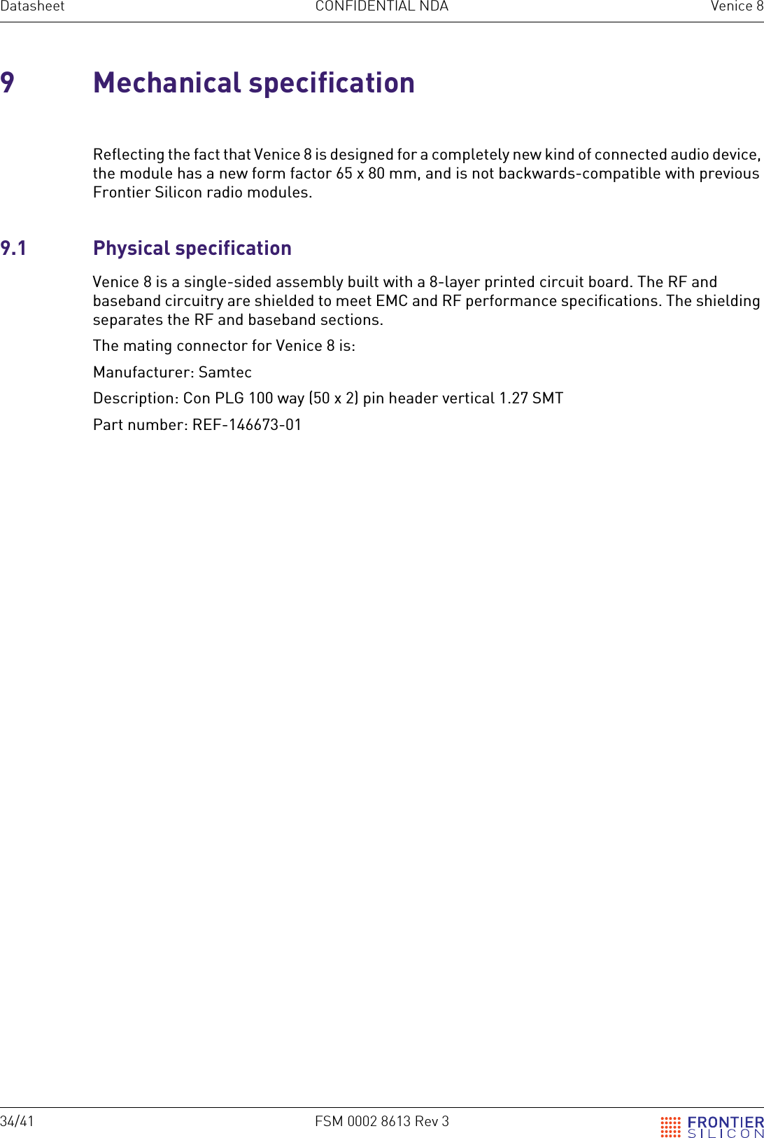
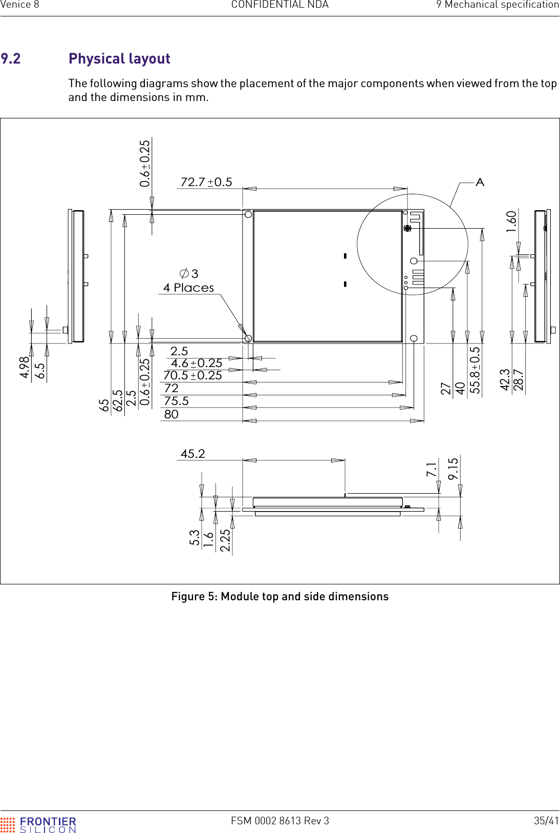
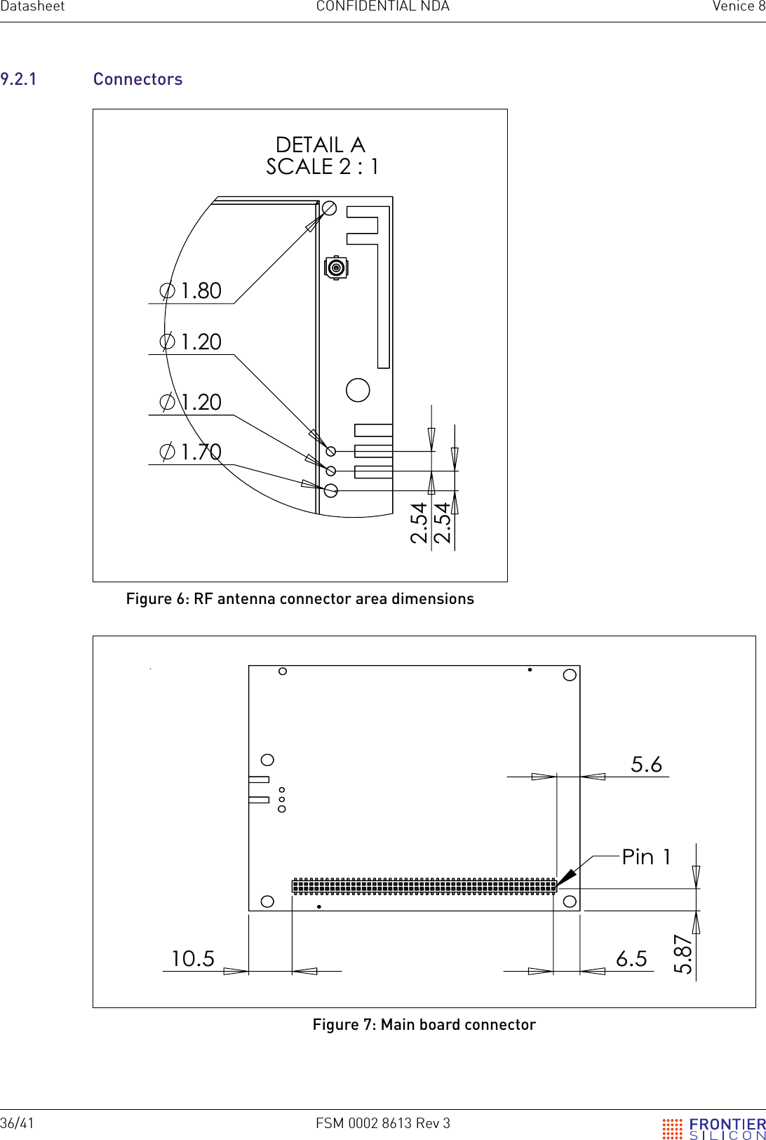
Frontier Silicon HA-FS2028-F Radio module supporting Internet Radio, Audio Streaming, iPod/iPhone control and FM-RDS reception User Manual Venice 8 Datasheet
Frontier Silicon Limited Radio module supporting Internet Radio, Audio Streaming, iPod/iPhone control and FM-RDS reception Venice 8 Datasheet
Venice8_DS
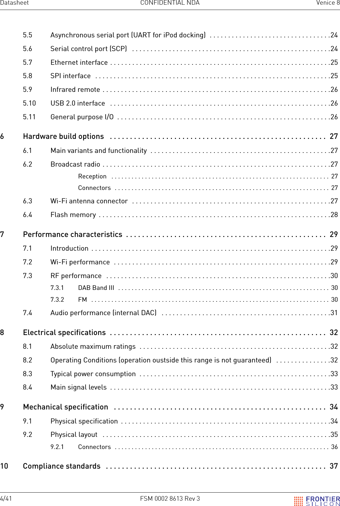
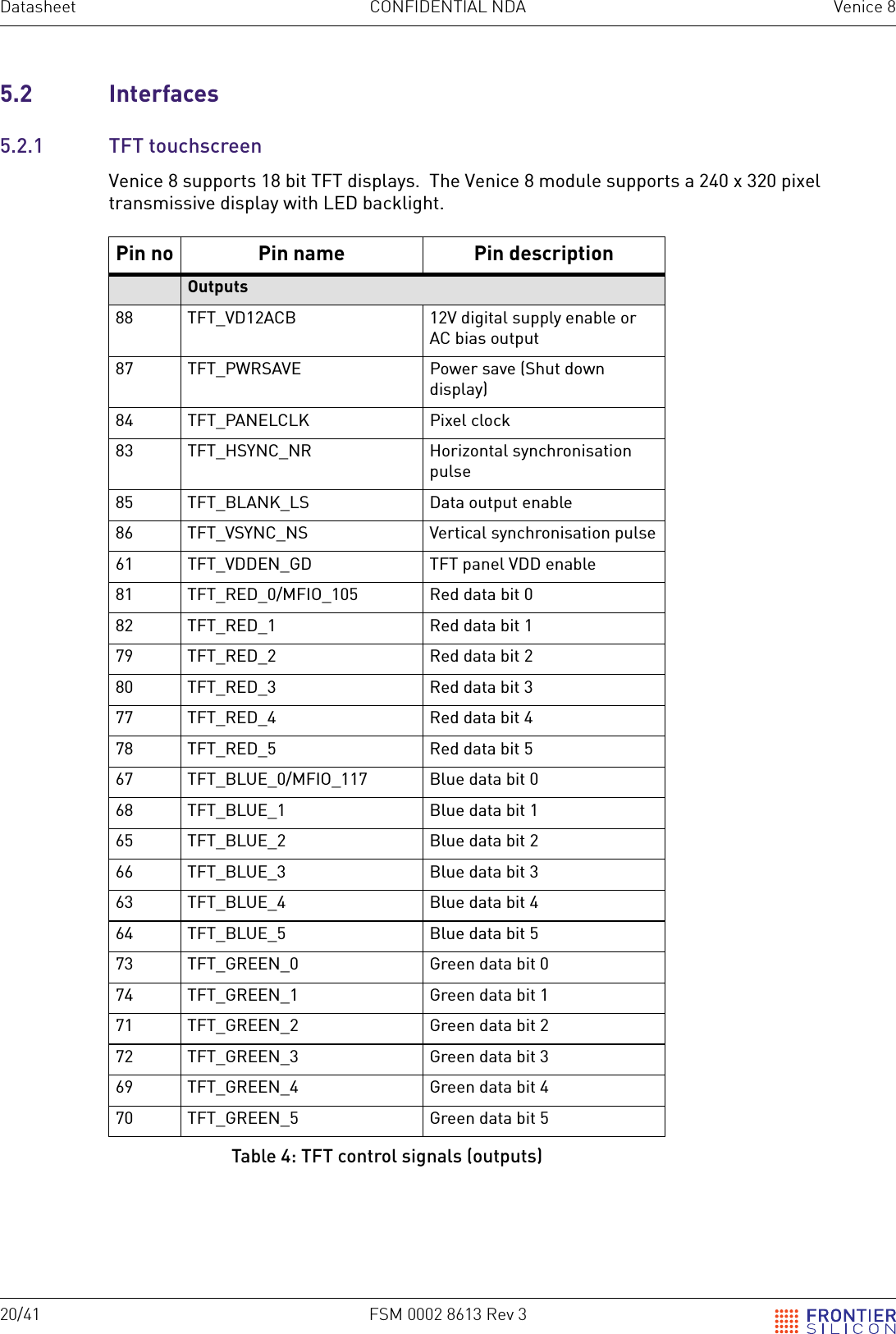
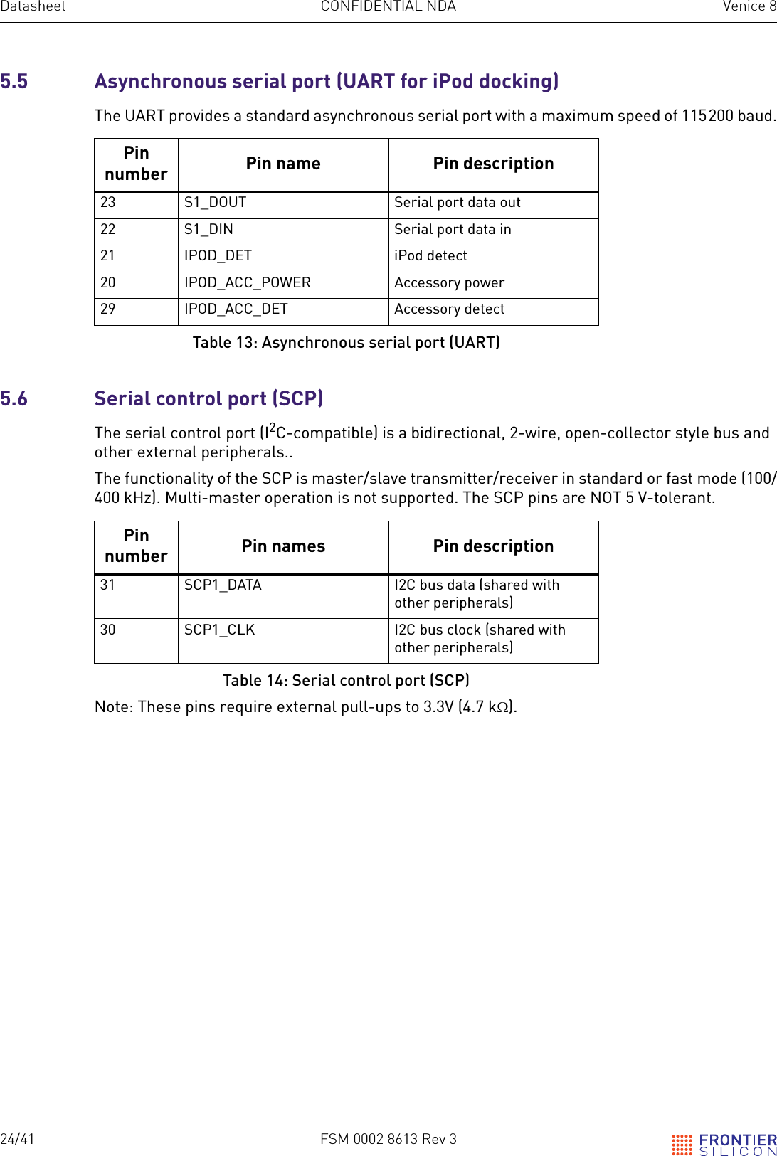
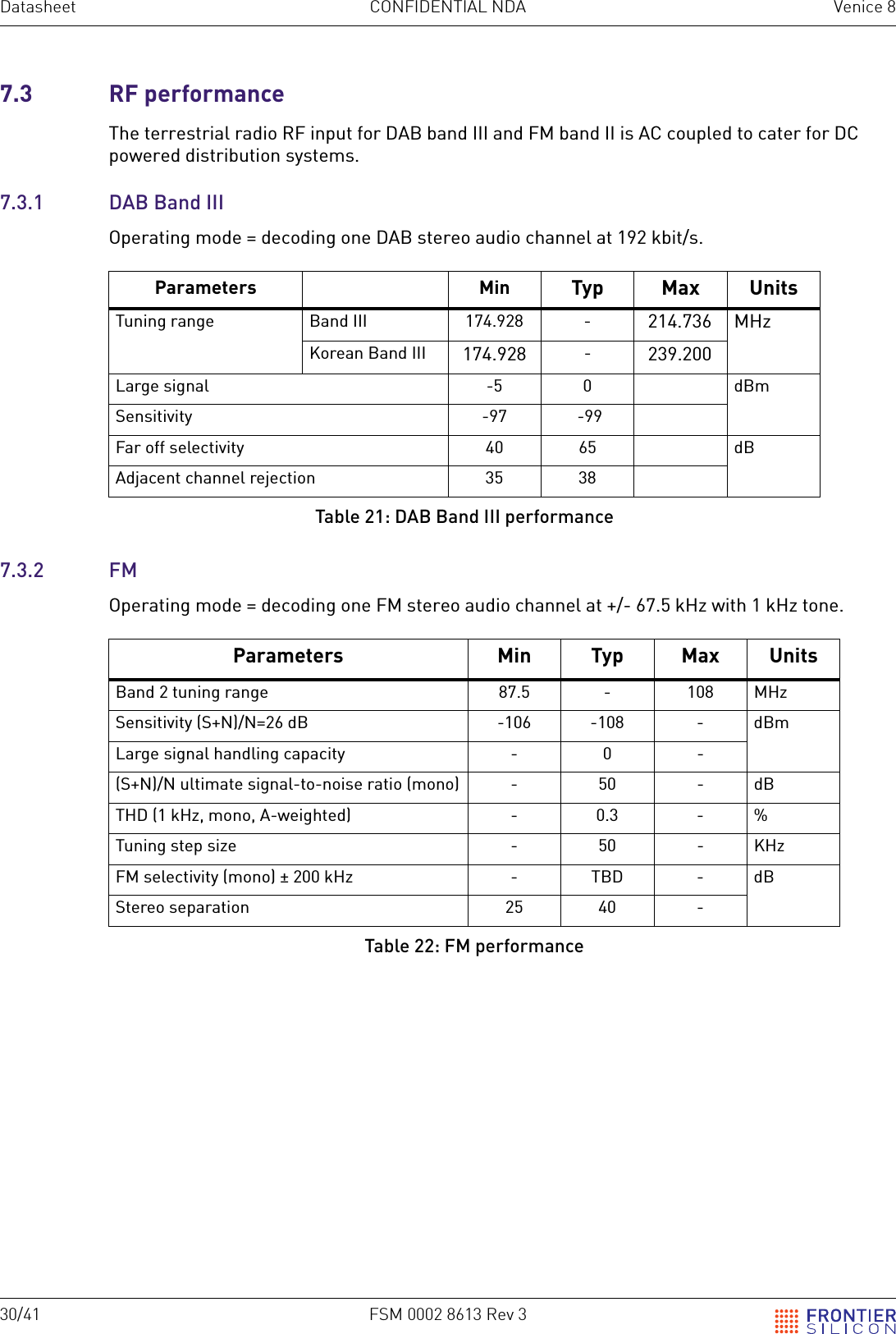
![FSM 0002 8613 Rev 3 29/41Venice 8 CONFIDENTIAL NDA 7 Performance characteristics7 Performance characteristics7.1 IntroductionVenice 8 is a Eureka 147 DAB receiver conforming to EN61000-4-2 supporting Band 3 and Korean Band 3 with typical performance equal to or better than EN50248:2001 [reference 9].Venice 8 supports Band 2 Soft FM (87.5 MHz to 108 MHz) and meets parts of the BS 5942-2:1987 Hi-Fidelity minimum performance when tested to BS 60315-4 [reference 10].For the following specifications, operating conditions are Ta = 25°C, VCC = 3.3 V.7.2 Wi-Fi performanceVenice 8 supports the mandatory modes required by 802.11b and 802.11g plus some optional modes, as listed in Table 20. The maximum transmit power of the Wi-Fi module is limited to 20 dBm Effective Isotropic Radiated Power (EIRP). The Wi-Fi module’s transmit power and the antenna gain added together must not exceed 20 dBm EIRP.For a nominal transmit power of 15 dBm, the minimum power is 12.5 dBm, and the maximum is 17 dBm.Standard Mode Bit rate, Mbit/sReceiver sensitivityMin Typ Units802.11b DSSS 1 -79 -92 dBm @ 8%PERDSSS 2 -79 -92HR/DSSS 5.5 -79 -91HR/DSSS 11 -79 -87802.11g ERP-OFDM 6 -82 -86 dBm @10% PER9-81-8512 -79 -8518 -77 -8424 -74 -8036 -70 -7948 -66 -7354 -65 -72Table 20: Wi-Fi performance](https://usermanual.wiki/Frontier-Silicon/HA-FS2028-F/User-Guide-1407542-Page-29.png)
![FSM 0002 8613 Rev 3 37/41Venice 8 CONFIDENTIAL NDA 10 Compliance standards10 Compliance standardsVenice 8 is designed to allow customers’ finished products to gain compliance with the following certifications:CE,Wi-Fi Alliance,DLNA 1.5,WWi,MFi,FCC.10.1 Electromagnetic compatibility (EMC)Venice 8 is tested in configurations representative of typical DAB consumer products to the following standards:BS EN 55013: 2001 for emissions,BS EN 55020: 2002 for immunity.The electromagnetic compatibility of a particular product is dependent upon the use and installation of the module within the product. Care should be taken to integrate the module with due regard to the effects of conducted and radiated signals.10.2 Electrostatic discharge (ESD) protectionVenice 8 is an ESD-sensitive device. It is tested to the standard EN61000 (4 kV on RF inputs).Special handling precautions should be used during manufacturing and testing.10.3 Restriction of hazardous substances (RoHS)All Frontier Silicon products meet the requirements of the EU RoHS directive 2002/95/EC RoHS, use RoHS-certified components and are assembled using lead-free processes. See the Frontier Silicon Declaration of Materials Compliance [reference 2].Additionally, Frontier Silicon adheres to best industry practice regarding the avoidance of environmentally harmful substances in products, above and beyond legal requirements such as RoHS.](https://usermanual.wiki/Frontier-Silicon/HA-FS2028-F/User-Guide-1407542-Page-37.png)
![40/41 FSM 0002 8613 Rev 3Datasheet CONFIDENTIAL NDA Venice 8GlossaryDAB Digital Audio BroadcastingFM Frequency ModulationGPIO General Purpose Input/OutputIC Integrated CircuitRDS (FM) Radio Data SystemSCP Serial Control ProtocolSPI Serial Peripheral InterfaceSPI master Provides SPI clock and initiates data transactions and requestsSPI slave Receives SPI clock and responds to data transactions and requestsS/PDIF Sony/Philips Digital InterfaceSRAM Static Random Access MemoryTFT Thin Film Transistor [display]UART Universal Asynchronous Receiver TransmitterUSB Universal Serial BusWWi Works With iPhone](https://usermanual.wiki/Frontier-Silicon/HA-FS2028-F/User-Guide-1407542-Page-40.png)