Frontier Silicon HA-FS2028-F Radio module supporting Internet Radio, Audio Streaming, iPod/iPhone control and FM-RDS reception User Manual Venice 8 Datasheet
Frontier Silicon Limited Radio module supporting Internet Radio, Audio Streaming, iPod/iPhone control and FM-RDS reception Venice 8 Datasheet
Venice8_DS
15 December 2010 FSM 0002 8613 Rev 3 1/41
Datasheet CONFIDENTIAL NDA Preliminary
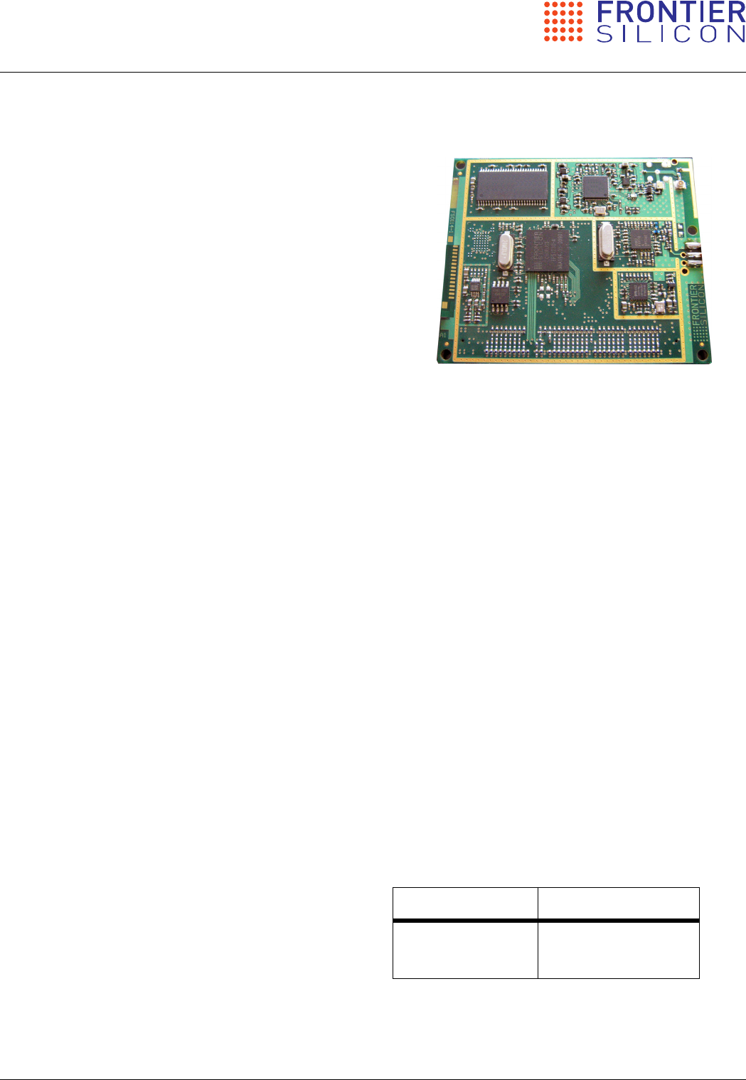
Venice 8 FS2028
Colour touchscreen connected audio module
Overview
The Venice 8 FS2028 module provides a colour
touch radio solution for Internet radio, home
network streaming, premium streaming content
services, DAB/DAB+/DMB-Radio and FM-RDS
products. It provides the simplest route to market
for premium high-quality audio streaming from live
Internet radio stations or network-based music
collections.
Several hardware and software configurations are
available, with different combinations of integrated
RF receivers for Wi-Fi networks, DAB Band III, FM
reception and Ethernet.
Based around Frontier Silicon’s Chorus 3
processor, Venice 8 streams radio stations and
music files in a variety of formats and protocols
including AAC+, MP3, Real and WMA, enabling a
new generation of stand-alone networked
touchscreen-based audio products.
Frontier Silicon also provides a complete reference
platform, Jupiter 8, for rapid evaluation of Venice 8
and development of Venice 8-based systems.
Applications include a wide range of audio
products, from kitchen and alarm clock radios to
CD micro systems, boomboxes and HiFi tuners.
Modes
• Live Internet radio broadcasts from over 12,000
radio stations
• Internet radio “listen again” on-demand content
• Music streaming from UPnP devices with
playlist capability
• Music streaming from USB stick
• Microsoft DRM 10 Streaming (on request)
• DAB Digital Audio Broadcast radio
• DAB+ with additional AAC+ codec
•DMB-Radio (on request)
• FM radio reception with RDS
Connectivity
• Wi-Fi 802.11b/g with WPS, WEP, WPA and WPA2
security
• Full colour graphical UI with touch driven
interface
• 10/100 Mb/s Ethernet
• USB 2.0 device or host
• On-board audio DAC with stereo analogue line
output
• Digital audio output -S/PDIF or I2S
• Infrared remote control
• Rotary encoder
Features
• Microsoft DRM 10 (digital rights management)
playback (on request)
• Codecs: MP3, WMA, AAC+, RealAudio, FLAC,
PCM and WAV
• Simple registration and configuration
• Remote control
•Internet portal
•Clock/alarms
• Automatically software upgradable in the field
through the Internet or via USB
• UPnP support
Ordering information
Further variants are described in Hardware build
options on page 27.
Product code Description
FS2028-WEB Wi-Fi, DAB, DAB+, DMB-
Radio, FM, Ethernet, USB
2.0, MP3, WMA, AAC+
2/41 FSM 0002 8613 Rev 3
Datasheet CONFIDENTIAL NDA Venice 8
Legal and precautionary notices
Copyright © 2010 Frontier Silicon Ltd. and its licensors. All Rights Reserved.
This document is confidential and proprietary to Frontier Silicon. It may not be copied nor its contents
disclosed without written permission from Frontier Silicon. All external recipient organisations must sign a
non-disclosure agreement.
This document supersedes all previous versions. In line with its policy of continuous improvement, Frontier
Silicon reserves the right to make changes to products and documentation without notice.
Frontier Silicon accepts no liability for any losses alleged to have arisen from use of this document or
associated products.
The Frontier Silicon logo is a trademark of Frontier Silicon.
MPEG-4 HE-AAC audio coding technology licensed by Fraunhofer IIS,
www.iis.fraunhofer.de.
DAB and MP3 technologies are subject to end-user patent licences: please
contact Frontier Silicon for more details.
Frontier Silicon Limited
137, Euston Road
London
NW1 2AA
United Kingdom
Tel: +44 207 391 0620
Fax: +44 207 388 6420
E-mail: info@frontier-silicon.com
Web: www.frontier-silicon.com
CAUTION: The product(s) described in this document contain static-
sensitive parts and must be handled in a static-controlled
environment.
Please see also the FCC statement in Section 10.4.

FSM 0002 8613 Rev 3 3/41
Venice 8 CONFIDENTIAL NDA
Contents
List of figures . . . . . . . . . . . . . . . . . . . . . . . . . . . . . . . . . . . . . . . . . . . . . . . . . . . . . . . . . . . . . . . . .6
List of tables . . . . . . . . . . . . . . . . . . . . . . . . . . . . . . . . . . . . . . . . . . . . . . . . . . . . . . . . . . . . . . . . . .7
Revision history . . . . . . . . . . . . . . . . . . . . . . . . . . . . . . . . . . . . . . . . . . . . . . . . . . . . . . . . . . . . . . .8
Document maturity key . . . . . . . . . . . . . . . . . . . . . . . . . . . . . . . . . . . . . . . . . . . . . . . . . . . . . . . .8
Feedback . . . . . . . . . . . . . . . . . . . . . . . . . . . . . . . . . . . . . . . . . . . . . . . . . . . . . . . . . . . . . . . . . . . .8
1 Applications . . . . . . . . . . . . . . . . . . . . . . . . . . . . . . . . . . . . . . . . . . . . . . . . . . . . . . . . . . . . . . . . . .9
2 Introduction . . . . . . . . . . . . . . . . . . . . . . . . . . . . . . . . . . . . . . . . . . . . . . . . . . . . . . . . . . . . . . . . 10
2.1 Features . . . . . . . . . . . . . . . . . . . . . . . . . . . . . . . . . . . . . . . . . . . . . . . . . . . . . . . . . . . . . . . . . . . .10
3 Power supplies . . . . . . . . . . . . . . . . . . . . . . . . . . . . . . . . . . . . . . . . . . . . . . . . . . . . . . . . . . . . . 12
3.1 Power-on timing . . . . . . . . . . . . . . . . . . . . . . . . . . . . . . . . . . . . . . . . . . . . . . . . . . . . . . . . . . . . .12
3.2 Power-off timing . . . . . . . . . . . . . . . . . . . . . . . . . . . . . . . . . . . . . . . . . . . . . . . . . . . . . . . . . . . . .12
3.3 Reset thresholds . . . . . . . . . . . . . . . . . . . . . . . . . . . . . . . . . . . . . . . . . . . . . . . . . . . . . . . . . . . . .12
3.4 Boot up considerations . . . . . . . . . . . . . . . . . . . . . . . . . . . . . . . . . . . . . . . . . . . . . . . . . . . . . . . .13
4 Software . . . . . . . . . . . . . . . . . . . . . . . . . . . . . . . . . . . . . . . . . . . . . . . . . . . . . . . . . . . . . . . . . . . 14
5 Hardware interfaces . . . . . . . . . . . . . . . . . . . . . . . . . . . . . . . . . . . . . . . . . . . . . . . . . . . . . . . . . 15
5.1 J6 main connector pin assignments . . . . . . . . . . . . . . . . . . . . . . . . . . . . . . . . . . . . . . . . . . . . .16
5.2 Interfaces . . . . . . . . . . . . . . . . . . . . . . . . . . . . . . . . . . . . . . . . . . . . . . . . . . . . . . . . . . . . . . . . . . .20
5.2.1 TFT touchscreen . . . . . . . . . . . . . . . . . . . . . . . . . . . . . . . . . . . . . . . . . . . . . . . . . . . . . . . . . . . . 20
5.2.2 Touchscreen interface . . . . . . . . . . . . . . . . . . . . . . . . . . . . . . . . . . . . . . . . . . . . . . . . . . . . . . . 21
5.2.3 Backlight control . . . . . . . . . . . . . . . . . . . . . . . . . . . . . . . . . . . . . . . . . . . . . . . . . . . . . . . . . . . 21
5.2.4 Rotary Encoder . . . . . . . . . . . . . . . . . . . . . . . . . . . . . . . . . . . . . . . . . . . . . . . . . . . . . . . . . . . . . 21
5.2.5 Key switches . . . . . . . . . . . . . . . . . . . . . . . . . . . . . . . . . . . . . . . . . . . . . . . . . . . . . . . . . . . . . . . 21
5.3 Analogue audio . . . . . . . . . . . . . . . . . . . . . . . . . . . . . . . . . . . . . . . . . . . . . . . . . . . . . . . . . . . . . .22
5.3.1 Analogue audio output . . . . . . . . . . . . . . . . . . . . . . . . . . . . . . . . . . . . . . . . . . . . . . . . . . . . . . . 22
5.3.2 Analogue inputs . . . . . . . . . . . . . . . . . . . . . . . . . . . . . . . . . . . . . . . . . . . . . . . . . . . . . . . . . . . . 22
5.4 Digital audio outputs . . . . . . . . . . . . . . . . . . . . . . . . . . . . . . . . . . . . . . . . . . . . . . . . . . . . . . . . . .23
5.4.1 I2S . . . . . . . . . . . . . . . . . . . . . . . . . . . . . . . . . . . . . . . . . . . . . . . . . . . . . . . . . . . . . . . . . . . . . . . 23
5.4.2 S/PDIF out . . . . . . . . . . . . . . . . . . . . . . . . . . . . . . . . . . . . . . . . . . . . . . . . . . . . . . . . . . . . . . . . . 23

4/41 FSM 0002 8613 Rev 3
Datasheet CONFIDENTIAL NDA Venice 8
5.5 Asynchronous serial port (UART for iPod docking) . . . . . . . . . . . . . . . . . . . . . . . . . . . . . . . . .24
5.6 Serial control port (SCP) . . . . . . . . . . . . . . . . . . . . . . . . . . . . . . . . . . . . . . . . . . . . . . . . . . . . . .24
5.7 Ethernet interface . . . . . . . . . . . . . . . . . . . . . . . . . . . . . . . . . . . . . . . . . . . . . . . . . . . . . . . . . . . .25
5.8 SPI interface . . . . . . . . . . . . . . . . . . . . . . . . . . . . . . . . . . . . . . . . . . . . . . . . . . . . . . . . . . . . . . . .25
5.9 Infrared remote . . . . . . . . . . . . . . . . . . . . . . . . . . . . . . . . . . . . . . . . . . . . . . . . . . . . . . . . . . . . . .26
5.10 USB 2.0 interface . . . . . . . . . . . . . . . . . . . . . . . . . . . . . . . . . . . . . . . . . . . . . . . . . . . . . . . . . . . .26
5.11 General purpose I/O . . . . . . . . . . . . . . . . . . . . . . . . . . . . . . . . . . . . . . . . . . . . . . . . . . . . . . . . . .26
6 Hardware build options . . . . . . . . . . . . . . . . . . . . . . . . . . . . . . . . . . . . . . . . . . . . . . . . . . . . . . 27
6.1 Main variants and functionality . . . . . . . . . . . . . . . . . . . . . . . . . . . . . . . . . . . . . . . . . . . . . . . . .27
6.2 Broadcast radio . . . . . . . . . . . . . . . . . . . . . . . . . . . . . . . . . . . . . . . . . . . . . . . . . . . . . . . . . . . . . .27
Reception . . . . . . . . . . . . . . . . . . . . . . . . . . . . . . . . . . . . . . . . . . . . . . . . . . . . . . . . . . . . . . . . . 27
Connectors . . . . . . . . . . . . . . . . . . . . . . . . . . . . . . . . . . . . . . . . . . . . . . . . . . . . . . . . . . . . . . . . 27
6.3 Wi-Fi antenna connector . . . . . . . . . . . . . . . . . . . . . . . . . . . . . . . . . . . . . . . . . . . . . . . . . . . . . .27
6.4 Flash memory . . . . . . . . . . . . . . . . . . . . . . . . . . . . . . . . . . . . . . . . . . . . . . . . . . . . . . . . . . . . . . .28
7 Performance characteristics . . . . . . . . . . . . . . . . . . . . . . . . . . . . . . . . . . . . . . . . . . . . . . . . . . 29
7.1 Introduction . . . . . . . . . . . . . . . . . . . . . . . . . . . . . . . . . . . . . . . . . . . . . . . . . . . . . . . . . . . . . . . . .29
7.2 Wi-Fi performance . . . . . . . . . . . . . . . . . . . . . . . . . . . . . . . . . . . . . . . . . . . . . . . . . . . . . . . . . . .29
7.3 RF performance . . . . . . . . . . . . . . . . . . . . . . . . . . . . . . . . . . . . . . . . . . . . . . . . . . . . . . . . . . . . .30
7.3.1 DAB Band III . . . . . . . . . . . . . . . . . . . . . . . . . . . . . . . . . . . . . . . . . . . . . . . . . . . . . . . . . . . . . . . 30
7.3.2 FM . . . . . . . . . . . . . . . . . . . . . . . . . . . . . . . . . . . . . . . . . . . . . . . . . . . . . . . . . . . . . . . . . . . . . . . 30
7.4 Audio performance (internal DAC) . . . . . . . . . . . . . . . . . . . . . . . . . . . . . . . . . . . . . . . . . . . . . .31
8 Electrical specifications . . . . . . . . . . . . . . . . . . . . . . . . . . . . . . . . . . . . . . . . . . . . . . . . . . . . . . 32
8.1 Absolute maximum ratings . . . . . . . . . . . . . . . . . . . . . . . . . . . . . . . . . . . . . . . . . . . . . . . . . . . .32
8.2 Operating Conditions (operation oustside this range is not guaranteed) . . . . . . . . . . . . . . .32
8.3 Typical power consumption . . . . . . . . . . . . . . . . . . . . . . . . . . . . . . . . . . . . . . . . . . . . . . . . . . . .33
8.4 Main signal levels . . . . . . . . . . . . . . . . . . . . . . . . . . . . . . . . . . . . . . . . . . . . . . . . . . . . . . . . . . . .33
9 Mechanical specification . . . . . . . . . . . . . . . . . . . . . . . . . . . . . . . . . . . . . . . . . . . . . . . . . . . . . 34
9.1 Physical specification . . . . . . . . . . . . . . . . . . . . . . . . . . . . . . . . . . . . . . . . . . . . . . . . . . . . . . . . .34
9.2 Physical layout . . . . . . . . . . . . . . . . . . . . . . . . . . . . . . . . . . . . . . . . . . . . . . . . . . . . . . . . . . . . . .35
9.2.1 Connectors . . . . . . . . . . . . . . . . . . . . . . . . . . . . . . . . . . . . . . . . . . . . . . . . . . . . . . . . . . . . . . . . 36
10 Compliance standards . . . . . . . . . . . . . . . . . . . . . . . . . . . . . . . . . . . . . . . . . . . . . . . . . . . . . . . 37

FSM 0002 8613 Rev 3 5/41
Venice 8 CONFIDENTIAL NDA
10.1 Electromagnetic compatibility (EMC) . . . . . . . . . . . . . . . . . . . . . . . . . . . . . . . . . . . . . . . . . . . .37
10.2 Electrostatic discharge (ESD) protection . . . . . . . . . . . . . . . . . . . . . . . . . . . . . . . . . . . . . . . . .37
10.3 Restriction of hazardous substances (RoHS) . . . . . . . . . . . . . . . . . . . . . . . . . . . . . . . . . . . . . .37
10.4 FCC statement . . . . . . . . . . . . . . . . . . . . . . . . . . . . . . . . . . . . . . . . . . . . . . . . . . . . . . . . . . . . . .38
10.4.1 Caution: Exposure to radio frequency radiation . . . . . . . . . . . . . . . . . . . . . . . . . . . . . . . . . . 38
10.4.2 Federal Communications Commission notice . . . . . . . . . . . . . . . . . . . . . . . . . . . . . . . . . . . . 38
10.4.3 Modifications . . . . . . . . . . . . . . . . . . . . . . . . . . . . . . . . . . . . . . . . . . . . . . . . . . . . . . . . . . . . . . . 38
10.5 RF exposure . . . . . . . . . . . . . . . . . . . . . . . . . . . . . . . . . . . . . . . . . . . . . . . . . . . . . . . . . . . . . . . .39
10.5.1 Occupational exposure levels . . . . . . . . . . . . . . . . . . . . . . . . . . . . . . . . . . . . . . . . . . . . . . . . . 39
10.5.2 General public exposure levels . . . . . . . . . . . . . . . . . . . . . . . . . . . . . . . . . . . . . . . . . . . . . . . . 39
Glossary. . . . . . . . . . . . . . . . . . . . . . . . . . . . . . . . . . . . . . . . . . . . . . . . . . . . . . . . . . . . . . . . . . . . 40

6/41 FSM 0002 8613 Rev 3
Datasheet CONFIDENTIAL NDA Venice 8
List of figures
Figure 1: Example master mode implementation. . . . . . . . . . . . . . . . . . . . . . . . . . . . . . . . . . . . .9
Figure 2: Module block diagram . . . . . . . . . . . . . . . . . . . . . . . . . . . . . . . . . . . . . . . . . . . . . . . . . .11
Figure 3: Main connector location and pin numbering scheme (rear view) . . . . . . . . . . . . . . .15
Figure 4: (front view) . . . . . . . . . . . . . . . . . . . . . . . . . . . . . . . . . . . . . . . . . . . . . . . . . . . . . . . . . . .15
Figure 5: Module top and side dimensions . . . . . . . . . . . . . . . . . . . . . . . . . . . . . . . . . . . . . . . . .35
Figure 6: RF antenna connector area dimensions . . . . . . . . . . . . . . . . . . . . . . . . . . . . . . . . . . .36
Figure 7: Main board connector . . . . . . . . . . . . . . . . . . . . . . . . . . . . . . . . . . . . . . . . . . . . . . . . . .36

FSM 0002 8613 Rev 3 7/41
Venice 8 CONFIDENTIAL NDA List of tables
List of tables
Table 1: Revision history. . . . . . . . . . . . . . . . . . . . . . . . . . . . . . . . . . . . . . . . . . . . . . . . . . . . . . . . . .8
Table 2: Reset threshold levels . . . . . . . . . . . . . . . . . . . . . . . . . . . . . . . . . . . . . . . . . . . . . . . . . . .12
Table 3: Main connector pin assignment . . . . . . . . . . . . . . . . . . . . . . . . . . . . . . . . . . . . . . . . . . .16
Table 4: TFT control signals (outputs) . . . . . . . . . . . . . . . . . . . . . . . . . . . . . . . . . . . . . . . . . . . . . .20
Table 5: Touchscreen interface . . . . . . . . . . . . . . . . . . . . . . . . . . . . . . . . . . . . . . . . . . . . . . . . . . .21
Table 6: Backlight control. . . . . . . . . . . . . . . . . . . . . . . . . . . . . . . . . . . . . . . . . . . . . . . . . . . . . . . .21
Table 7: Rotary encoder . . . . . . . . . . . . . . . . . . . . . . . . . . . . . . . . . . . . . . . . . . . . . . . . . . . . . . . . .21
Table 8: Key switches . . . . . . . . . . . . . . . . . . . . . . . . . . . . . . . . . . . . . . . . . . . . . . . . . . . . . . . . . . .21
Table 9: Analogue audio output . . . . . . . . . . . . . . . . . . . . . . . . . . . . . . . . . . . . . . . . . . . . . . . . . . .22
Table 10: Analogue inputs . . . . . . . . . . . . . . . . . . . . . . . . . . . . . . . . . . . . . . . . . . . . . . . . . . . . . . . .22
Table 11: I2S bus signals . . . . . . . . . . . . . . . . . . . . . . . . . . . . . . . . . . . . . . . . . . . . . . . . . . . . . . . . .23
Table 12: S/PDIF audio output . . . . . . . . . . . . . . . . . . . . . . . . . . . . . . . . . . . . . . . . . . . . . . . . . . . . .23
Table 13: Asynchronous serial port (UART) . . . . . . . . . . . . . . . . . . . . . . . . . . . . . . . . . . . . . . . . . .24
Table 14: Serial control port (SCP) . . . . . . . . . . . . . . . . . . . . . . . . . . . . . . . . . . . . . . . . . . . . . . . . .24
Table 15: Ethernet interface. . . . . . . . . . . . . . . . . . . . . . . . . . . . . . . . . . . . . . . . . . . . . . . . . . . . . . .25
Table 16: SPI interface . . . . . . . . . . . . . . . . . . . . . . . . . . . . . . . . . . . . . . . . . . . . . . . . . . . . . . . . . . .25
Table 17: Infrared remote. . . . . . . . . . . . . . . . . . . . . . . . . . . . . . . . . . . . . . . . . . . . . . . . . . . . . . . . .26
Table 18: USB 2.0 interface . . . . . . . . . . . . . . . . . . . . . . . . . . . . . . . . . . . . . . . . . . . . . . . . . . . . . . .26
Table 19: Venice 8 main variants and functionality . . . . . . . . . . . . . . . . . . . . . . . . . . . . . . . . . . . .27
Table 20: Wi-Fi performance . . . . . . . . . . . . . . . . . . . . . . . . . . . . . . . . . . . . . . . . . . . . . . . . . . . . . .29
Table 21: DAB Band III performance . . . . . . . . . . . . . . . . . . . . . . . . . . . . . . . . . . . . . . . . . . . . . . . .30
Table 22: FM performance . . . . . . . . . . . . . . . . . . . . . . . . . . . . . . . . . . . . . . . . . . . . . . . . . . . . . . . .30
Table 23: Audio analogue output . . . . . . . . . . . . . . . . . . . . . . . . . . . . . . . . . . . . . . . . . . . . . . . . . . .31
Table 24: Absolute maximum ratings . . . . . . . . . . . . . . . . . . . . . . . . . . . . . . . . . . . . . . . . . . . . . . .32
Table 25: Operating conditions. . . . . . . . . . . . . . . . . . . . . . . . . . . . . . . . . . . . . . . . . . . . . . . . . . . . .32
Table 26: Typical power consumption . . . . . . . . . . . . . . . . . . . . . . . . . . . . . . . . . . . . . . . . . . . . . . .33
Table 27: Main signal levels . . . . . . . . . . . . . . . . . . . . . . . . . . . . . . . . . . . . . . . . . . . . . . . . . . . . . . .33

8/41 FSM 0002 8613 Rev 3
Datasheet CONFIDENTIAL NDA Venice 8
Revision history
Document maturity key
Initial Initial data, all subject to change.
Preliminary Preliminary data; minor details may be missing or subject to change.
Complete All sections complete.
Revised Additions/corrections incorporated.
Obsolete Document refers to a discontinued or soon-to-be-discontinued product.
Withdrawn from external distribution.
Feedback
To contribute feedback on this document, please e-mail
technical-publications@frontier-silicon.com.
Include the following information:
• document title, number and date:
Venice 8 FS2028 Datasheet, FSM 0002 8613 Rev 3, 15 December 2010,
• section number and heading if referring to a specific part of the document.
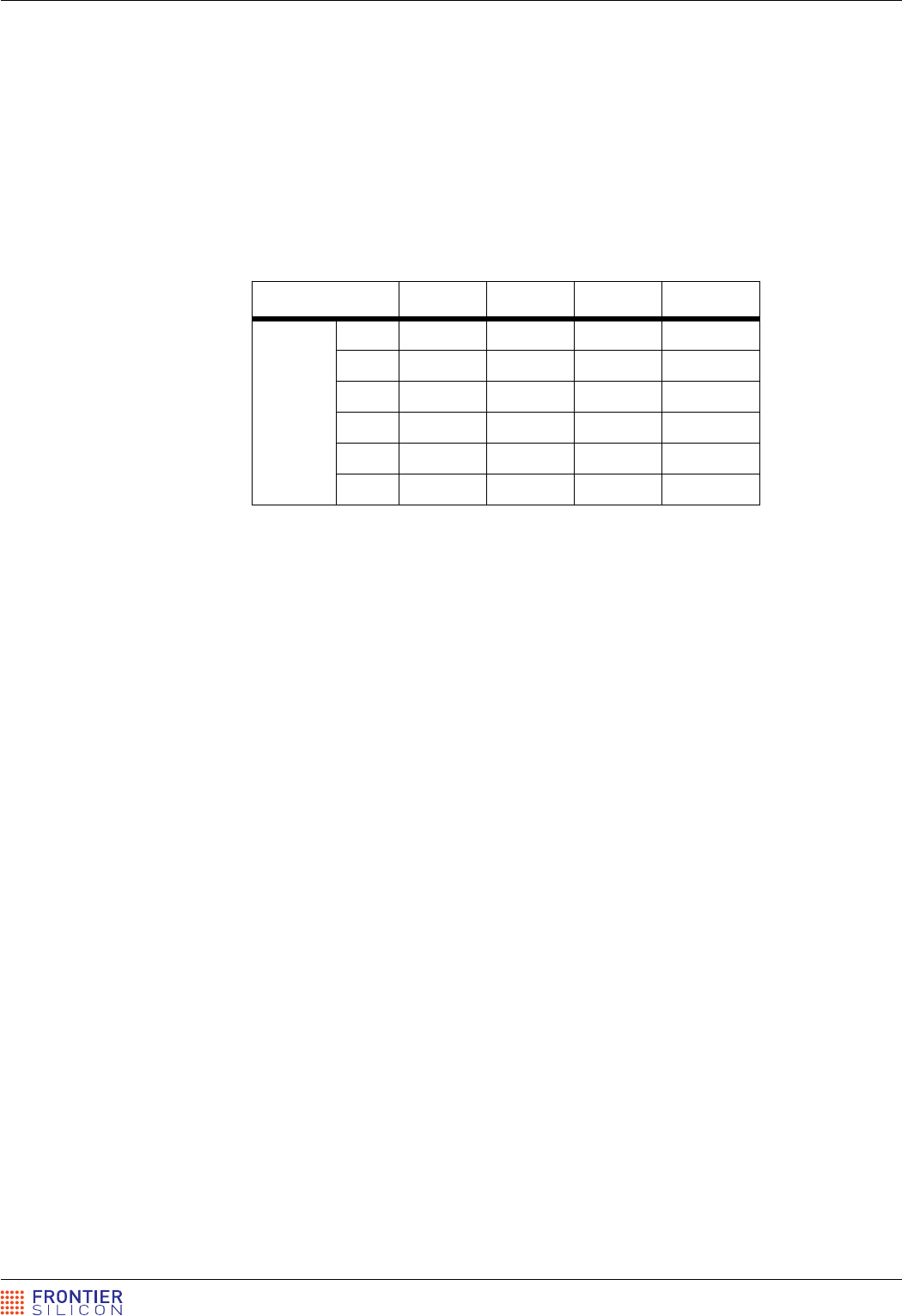
Revision
number Date Document
maturity Description
1 December 2009 Initial First release
2 December 2010 Preliminary FCC statement added to Compliance Standards; other
minor changes made
3 December 2010 Preliminary Changes made to FCC statement.
Table 1: Revision history
FSM 0002 8613 Rev 3 9/41
Venice 8 CONFIDENTIAL NDA 1 Applications
1 Applications
Venice 8 is designed for high-end mains-powered colour GUI connected audio products
including:
• Colour touch Internet radio,
•Kitchen radio,
•Clock radio,
•Table top,
•Semi-portable,
• Tuner products,
• Hi-fi or micro system.
Digital radio and premium streaming audio services’ availability varies by country, so different
markets require different hardware and software builds of the module. The main target markets
for Venice 8-based systems currently include the US, UK, Europe and Australia.
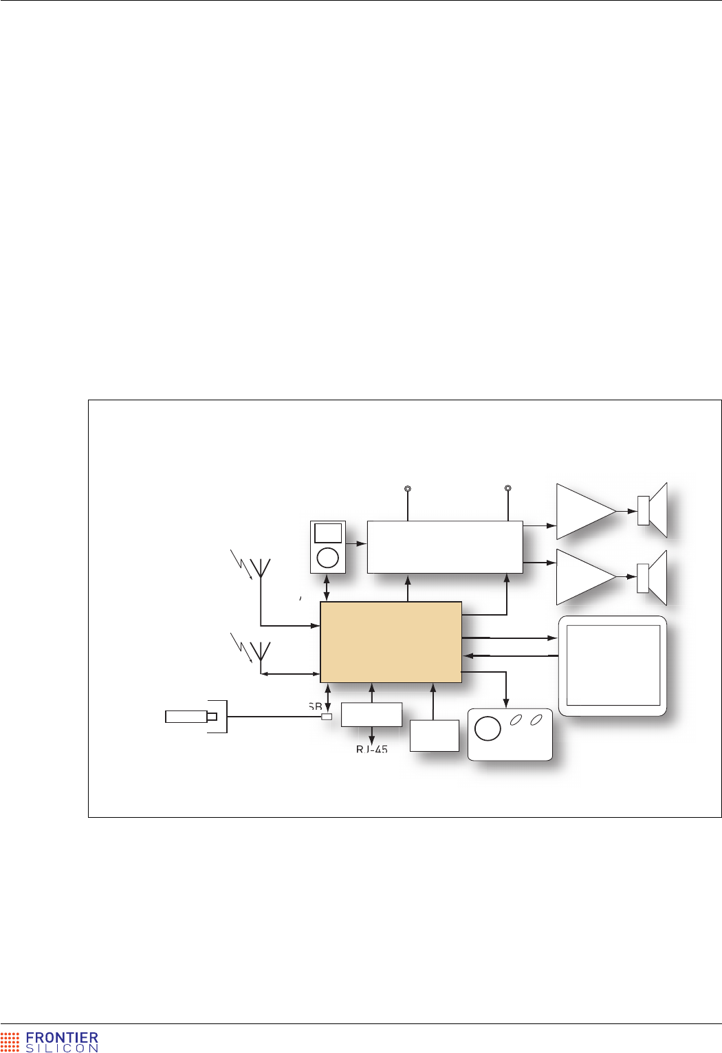
Figure 1 shows a typical implementation, with the module functioning as main system controller.
Figure 1: Example master mode implementation
Aux in Line out
DAB/
FM
Function select, volume
+ Preset EQ
Wi-Fi
Flash
stick
USB
Touchscreen
TFT colour
display
Venice 8
RJ-45
UART
iPod dock
Magnetics
IR
receiver
Backlight
Controls

10/41 FSM 0002 8613 Rev 3
Datasheet CONFIDENTIAL NDA Venice 8
2 Introduction
Venice 8 has been designed as the next step in the evolution of connected audio products. Based
around the new Frontier Silicon Chorus 3 baseband audio processor, it builds on the
functionality of the Venice 6.2 Internet radio module to facilitate a new type of touchscreen
connected audio product, with new features, performance and ergonomics ensuring the highest
possible performance.
Venice 8 features a new, highly customisable UI, making full use of the latest TFT display
technology with resistive touch, to improve ease-of-use.
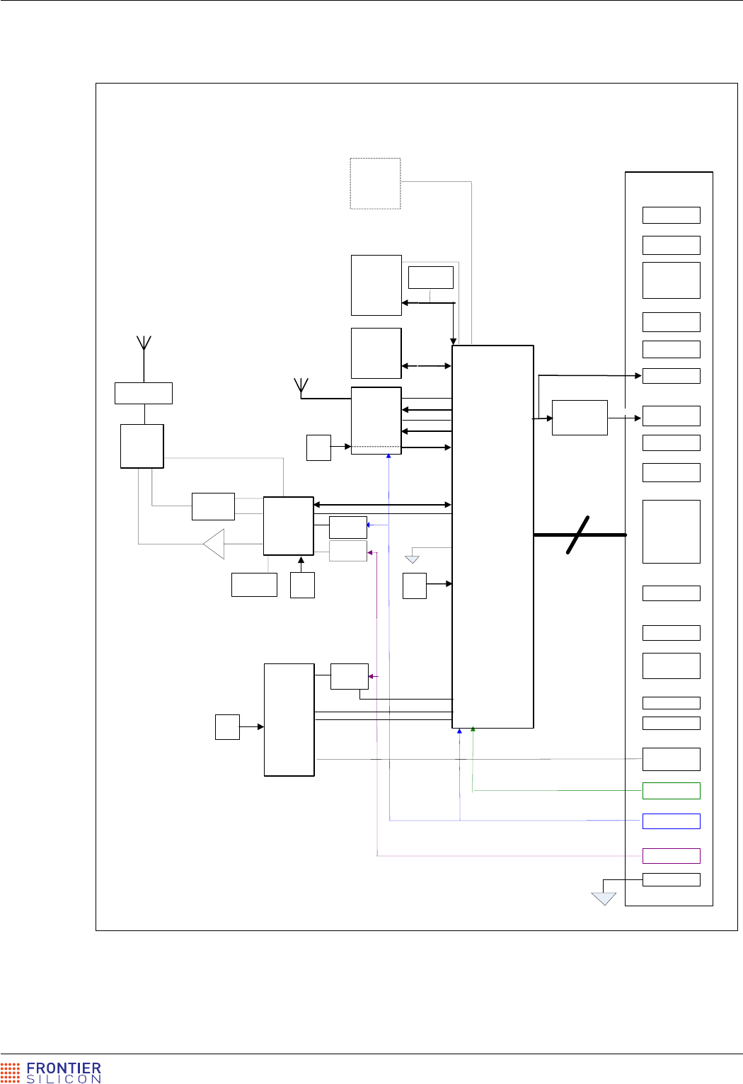
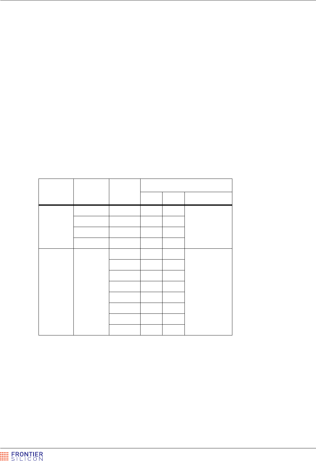
2.1 Features
Figure 2 shows a block diagram of Venice 8. The main components are the RF front end,
Chorus 3 FS1230 baseband processor, serial boot Flash, SDRAM and audio DAC.
The Chorus 3 processor is based around a high performance advanced RISC/DSP. In addition to
the core DAB demodulation functions, this processor is well suited to running digital radio/
connected audio application code.
Venice 8 measures 65 x 80 mm (see Chapter 9: Mechanical specification). All components are
mounted on the top of the module. The underside of the module has a solid copper ground plane.
With the exception of the connectors and screw holes, all components are fitted inside the four-
chamber screening can. The RF, Wi-Fi, baseband and analogue audio sections are all screened
from each other.
Venice 8 has been designed to use a 3.5 inch TFT colour touchscreen module with a resolution
of QVGA (320 x 240) and an LED backlight.
Stereo audio outputs are provided in analogue line level and S/PDIF digital formats
Venice 8 has two MAC addresses, one for Wi-Fi and one for Ethernet. It is supplied with 4 MAC
address labels for the Wi-Fi (the Ethernet MAC address is the Wi-Fi MAC address plus one).
FSM 0002 8613 Rev 3 11/41
Venice 8 CONFIDENTIAL NDA 2 Introduction
Figure 2: Module block diagram
Audio
DAC / Amp
analog
+3V3 Supply
RF IC:
APOLLO
2
Band2,3
Antenna
CHORUS 3
WiFi
circuit
WiFi
Antenna
TFT/LCD
Display Parallel
Interface
USB 2.0 HS
+1V2 Supply
FLASH
ROM
64Mb
MAIN
CONNECTOR
XTAL
24.576MHz
XTAL
38.4MHz
(Analog IF)
USB XTAL
Switch
SPI4
64M B
SDRAM
SYS_nRST
I2C
GNDs
IR control
SPI2 (TFT)
I2S In/Out
UART1
+5V Supply
Ethernet
PHY
Ethernet
XTAL
25.0MHz
ADC2
ADC1
PDM
Future
option,
512Mbit
Nand
Flash
L,R,Gnd
Out
SPDIF
GPIO
3V3
LDO
Test
Points
24.576MHz
(I2C)
(IF AGC)
(Enable)
(MII)
Band Pass
Filter
Balun
PA
Ant Control
WLAN RX
WLAN Tx
Test
Points
Serial Port
1V8
LDO
(Reset, Int)
(Fast Switch)
(GPIO)
(GPIO)
(CS1,CLK,MOSI,MISO)
1 (DRM)
3V3
LDO
I2S
Venice 8 M odule
FS2028
MFIO
12/41 FSM 0002 8613 Rev 3
Datasheet CONFIDENTIAL NDA Venice 8
3 Power supplies
Venice 8 requires a 1.2 V ± 5%, supply for the digital baseband and 3.3 V ± 5% for the RF circuits
and other baseband devices such as the audio DAC and 5 V ± 5% for Wi-Fi and Ethernet . All
supplies should be clean with low ripple. Any noise on these supplies will affect performance.
The module includes some supply filtering on its DC supply lines. This takes the form of a Pi
network with a ferrite bead inductor in the supply line and with one or more capacitors to ground
on either side.
The voltage rails must be regulated with over-specified regulators and bulk decoupling to cope
with the burst requirements of the DAB receiver, Wi-Fi TX and to reduce noise and ripple. The
capacitors and regulators should be mounted as close as possible to J1.
For best performance, the system PCB should include a solid ground plane. If this is not
possible, the PCB should use large power tracks, with the ground connections from each
regulator and smoothing capacitor joining close to the module.
3.1 Power-on timing
The 5.0 V, 3.3 V and 1.2 V supplies may be applied in any order but extended periods of delay
should be avoided.
3.2 Power-off timing
Venice 8 is designed so that the power can be removed in any order at any time without affecting
the module.
3.3 Reset thresholds
The 1.2 V, 3V3 and 5V supplies to Venice 8 should be kept within the operating limits. The
module’s operation may become unstable if the supply deviates from these limits.
Venice 8 incorporates an on-board reset to cope with supply interruptions.
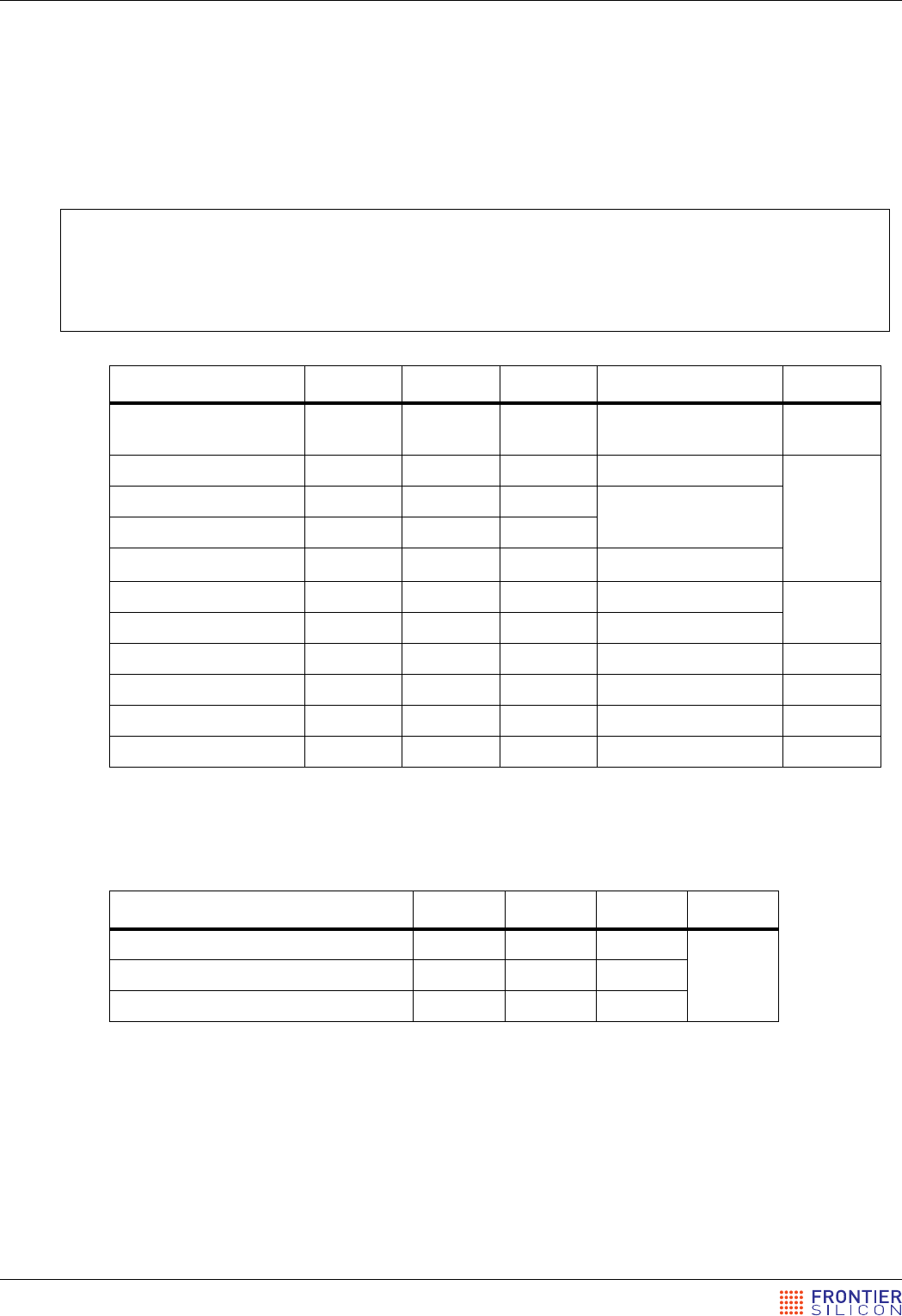
Supply Symbol Parameter Typ Units
3.3V VTH+ Reset threshold rising level 2.25 V
VTH- Reset threshold falling level 2.15
1.2V VTH+ Reset threshold rising level 0.95
VTH- Reset threshold falling level 0.90
Table 2: Reset threshold levels

FSM 0002 8613 Rev 3 13/41
Venice 8 CONFIDENTIAL NDA 3 Power supplies
3.4 Boot up considerations
1. Care must be taken to ensure that SPDIF_OUT (pin 19) is driven low during the reset cycle.
2. USB_VBUS_FAULT (pin 38) must not have any external pull-ups fitted as there is a 100 kΩ in
the module. Failure to do this will result in boot up problems.

14/41 FSM 0002 8613 Rev 3
Datasheet CONFIDENTIAL NDA Venice 8
4 Software
Frontier Silicon normally provides Venice 8 pre-installed with software. This can be configured
to customer requirements.
The module is intended to be used as the basis for a standalone connected audio system (see
Figure 1 on page 9). The only external parts needed are a power source, antenna(s), TFT touchpad
display, infrared receiver, backlight, iPod authentication, keypad (two switches), rotary encoder
(optional), amplifier and speaker(s).
Soft FM (RDS) software allows the module to function as an FM radio receiver without the need
for a separate FM tuner chip. An FM user interface provides access to all RDS features.
Please contact Frontier Silicon for further information.
FSM 0002 8613 Rev 3 15/41
Venice 8 CONFIDENTIAL NDA 5 Hardware interfaces
5 Hardware interfaces
Venice 8 supports numerous hardware interfaces (physical layout shown in Section 9.2.1). The
characteristics of these interfaces are detailed below.
Note: Some of these interfaces may be mutually exclusive.
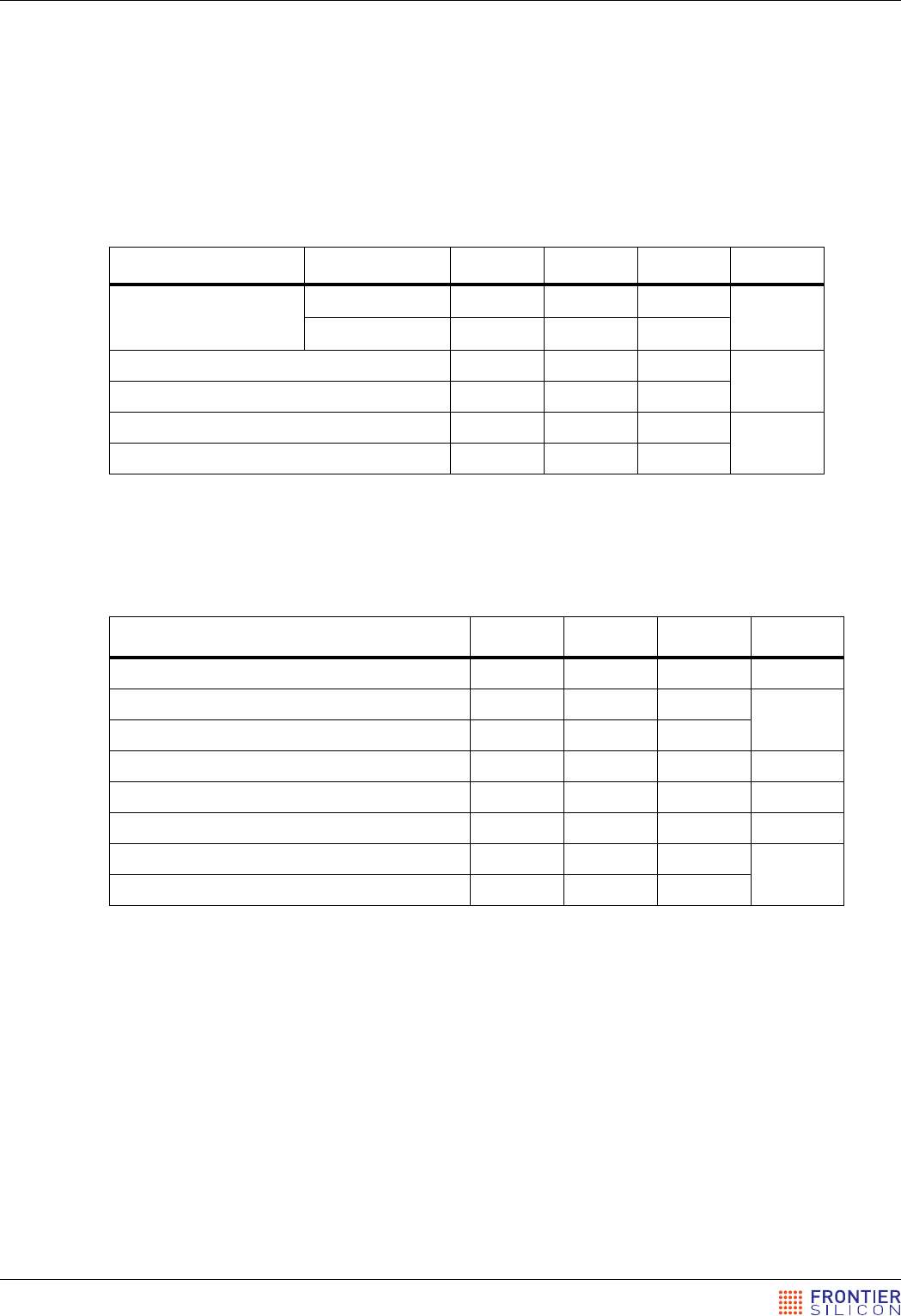
Figure 3: Main connector location and pin numbering scheme (rear view)
Figure 4: (front view)
1
2
35
46
7
8
....
........
99 97 95
100 98 96
....
J6 (main connector)
J5
J4
J3

16/41 FSM 0002 8613 Rev 3
Datasheet CONFIDENTIAL NDA Venice 8
5.1 J6 main connector pin assignments
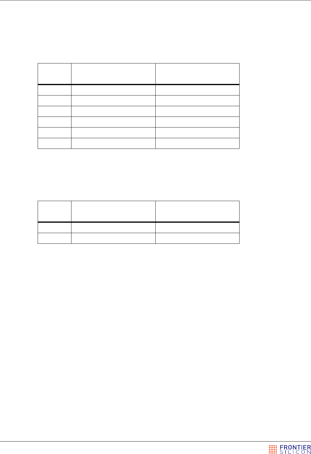
Pin no Pin name Usage Alternative
Usage Drive (mA)
1 5V_Input 5V supply - -
2 1V2_Input 1.2 supply - -
3GND Ground - -
4 3V3_Input 3.3V supply - -
5 AUD_L Analogue output left - DAC
6 AUD_R Analogue output right - DAC
7GND Ground - -
8AUD_GND Audio ground - -
9I2S_MCLK_FILT I2S GPIO 4
10 GND Ground - -
11 I2S_SCLK_FILT I2S GPIO 4
12 I2S_SFR_FILT I2S GPIO 4
13 I2S_SDIN I2S GPIO 4
14 I2S_SDOUT0_FILT I2S GPIO 4
15 AUDIO_MUTE Audio control GPIO 4
16 AUDIO_AMP_ON Audio control GPIO 4
17 HEADPHONE_DET Audio control GPIO 8
18 SPDIF_PWR_SW SPDIF GPIO 4
19 SPDIF_OUT SPDIF GPIO 4
20 IPOD_ACC_POWER iPod GPIO 4
21 IPOD_DET iPod GPIO 4
22 S1_DIN iPod GPIO 4
23 S1_DOUT iPod GPIO 8
24 SPI1_SCK_F SPI - 4
25 SPI1_MISO2 SPI GPIO 8
26 SPI1_MOSI_F SPI - 4
27 SPI_CSn4 SPI GPIO 8
28 SPI_CSn2 SPI GPIO 4
29 SPI1_MISO4/
IPOD_ACC_DET
iPod GPIO 8
30 SCP1_CLK I2C GPIO 8
31 SCP1_DATA I2C GPIO 8
32 GND Ground - -
Table 3: Main connector pin assignment

FSM 0002 8613 Rev 3 17/41
Venice 8 CONFIDENTIAL NDA 5 Hardware interfaces
33 USB_DP USB D+ - A
34 USB_DN USB D- - A
35 USB_VBUS USB - A
36 USB_COM Ground - -
37 USB_VBUS_DRIVE USB GPIO 4
38 USB_VBUS_FAULT USB GPIO 4
39 GND Ground Ground -
40 GP_ADC1 Analogue input - A
41 GP_ADC0 Analogue input - A
42 SYS_nRST Module reset - 8
43 IR_REMOTE IR GPIO 8
44 KYBRD_COL_2 GPIO GPIO 8
45 KYBRD_COL_1 GPIO GPIO 8
46 KYBRD_COL_4 GPIO GPIO 8
47 KYBRD_COL_3 GPIO GPIO 8
48 KYBRD_ROW_2 GPIO GPIO 8
49 KYBRD_ROW_1 GPIO GPIO 8
50 MFIO_87 GPIO - 4
51 MFIO_85 GPIO - 8
52 MFIO_86 GPIO - 8
53 MFIO_82 GPIO - 8
54 MFIO_81 GPIO - 8
55 MFIO_83 GPIO - 8
56 MFIO_84 GPIO - 8
57 MFIO_88 GPIO - 4
58 MFIO_73 GPIO - 8
59 GND Ground - -
60 MFIO_89 GPIO - 4
61 TFT_VDDEN_GD TFT Display GPIO 4
62 GND Ground - -
63 TFT_BLUE_4 TFT Display GPIO 4
64 TFT_BLUE_5 TFT Display GPIO 4
Pin no Pin name Usage Alternative
Usage Drive (mA)
Table 3: Main connector pin assignment

18/41 FSM 0002 8613 Rev 3
Datasheet CONFIDENTIAL NDA Venice 8
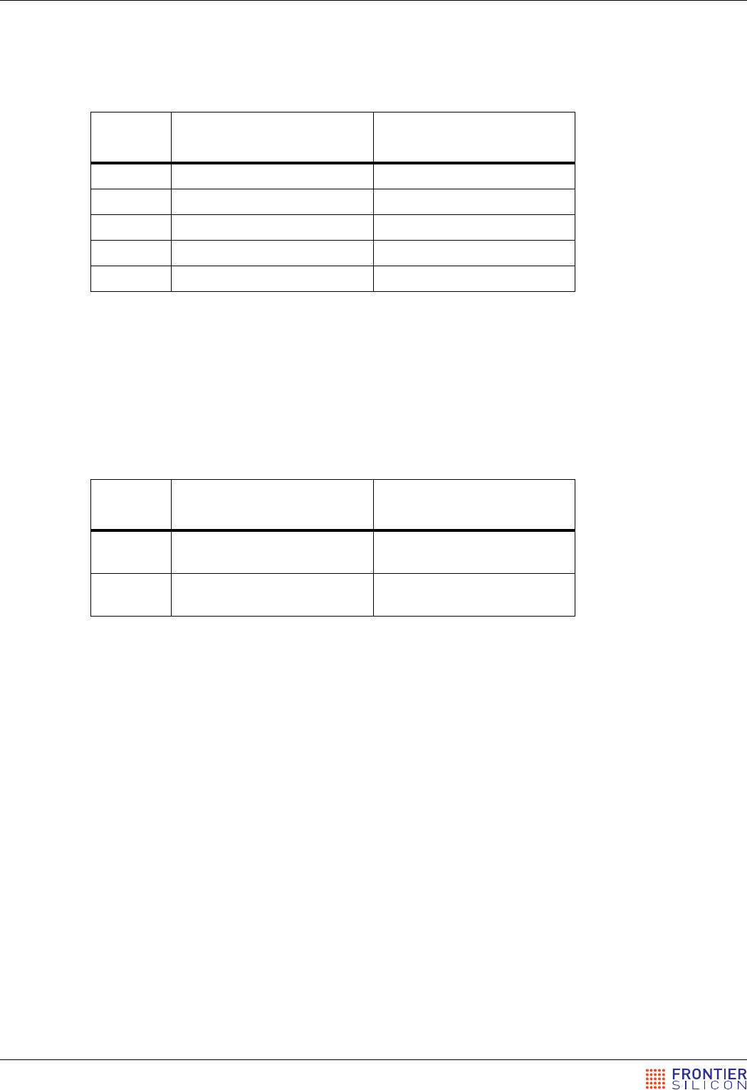
65 TFT_BLUE_2 TFT Display GPIO 4
66 TFT_BLUE_3 TFT Display GPIO 4
67 TFT_BLUE_0/
MFIO_117
TFT Display GPIO 4
68 TFT_BLUE_1 TFT Display GPIO 4
69 TFT_GREEN_4 TFT Display GPIO 4
70 TFT_GREEN_5 TFT Display GPIO 4
71 TFT_GREEN_2 TFT Display GPIO 4
72 TFT_GREEN_3 TFT Display GPIO 4
73 TFT_GREEN_0 TFT Display GPIO 4
74 TFT_GREEN_1 TFT Display GPIO 4
75 GND Ground - -
76 GND Ground - -
77 TFT_RED_4 TFT Display GPIO 4
78 TFT_RED_5 TFT Display GPIO 4
79 TFT_RED_2 TFT Display GPIO 4
80 TFT_RED_3 TFT Display GPIO 4
81 TFT_RED_0/MFIO_105 TFT Display GPIO 4
82 TFT_RED_1 TFT Display GPIO 4
83 TFT_HSYNC_NR TFT Display GPIO 4
84 TFT_PANELCLK TFT Display GPIO 4
85 TFT_BLANK_LS TFT Display GPIO 4
86 TFT_VSYNC_NS TFT Display GPIO 4
87 TFT_PWRSAVE TFT Display GPIO 4
88 TFT_VD12ACB TFT Display GPIO 4
89 DIM_F PDM GPIO 4
90 TOUCH_SCR_INTn_F GPIO GPIO 4
91 GND Ground - -
92 GND Ground - -
93 ETH_TX+ Ethernet - PHY
94 ETH_SPEED Ethernet LED - PHY
95 ETH_GND Ground - PHY
96 ETH_TX- Ethernet - PHY
97 ETH_RX+ Ethernet - PHY
98 ETH_CT Ethernet - PHY
Pin no Pin name Usage Alternative
Usage Drive (mA)
Table 3: Main connector pin assignment

20/41 FSM 0002 8613 Rev 3
Datasheet CONFIDENTIAL NDA Venice 8
5.2 Interfaces
5.2.1 TFT touchscreen
Venice 8 supports 18 bit TFT displays. The Venice 8 module supports a 240 x 320 pixel
transmissive display with LED backlight.
Pin no Pin name Pin description
Outputs
88 TFT_VD12ACB 12V digital supply enable or
AC bias output
87 TFT_PWRSAVE Power save (Shut down
display)
84 TFT_PANELCLK Pixel clock
83 TFT_HSYNC_NR Horizontal synchronisation
pulse
85 TFT_BLANK_LS Data output enable
86 TFT_VSYNC_NS Vertical synchronisation pulse
61 TFT_VDDEN_GD TFT panel VDD enable
81 TFT_RED_0/MFIO_105 Red data bit 0
82 TFT_RED_1 Red data bit 1
79 TFT_RED_2 Red data bit 2
80 TFT_RED_3 Red data bit 3
77 TFT_RED_4 Red data bit 4
78 TFT_RED_5 Red data bit 5
67 TFT_BLUE_0/MFIO_117 Blue data bit 0
68 TFT_BLUE_1 Blue data bit 1
65 TFT_BLUE_2 Blue data bit 2
66 TFT_BLUE_3 Blue data bit 3
63 TFT_BLUE_4 Blue data bit 4
64 TFT_BLUE_5 Blue data bit 5
73 TFT_GREEN_0 Green data bit 0
74 TFT_GREEN_1 Green data bit 1
71 TFT_GREEN_2 Green data bit 2
72 TFT_GREEN_3 Green data bit 3
69 TFT_GREEN_4 Green data bit 4
70 TFT_GREEN_5 Green data bit 5
Table 4: TFT control signals (outputs)
FSM 0002 8613 Rev 3 21/41
Venice 8 CONFIDENTIAL NDA 5 Hardware interfaces
5.2.2 Touchscreen interface
5.2.3 Backlight control
Backlight control of the LCD can be achieved using a Linear Tech LT3465 which varies the
current provided to the backlight with an analogue voltage. On Venice 8 a PDM output is
converted to an analogue voltage using an onboard RC filter.
5.2.4 Rotary Encoder
Two GPIO are dedicated to implement a rotary encoder for volume control. The push to mute or
select function is implemented as on of the dedicated Key Switches.
5.2.5 Key switches
Four GPIO are dedicated for key switches to interact with the UI.
Pin no Pin name Pin description
90 TOUCH_SCR_INTn_F Touchscreen pen down
interrupt
30 SCP_CLK I2C bus clock (shared with
other peripherals)
31 SCP1_DAT I2C bus clock (shared with
other peripherals)
Table 5: Touchscreen interface
Pin no Pin name Pin description
89 DIM_F Backlight control. Pulse
density modulated output1
filtered to an analogue voltage
Table 6: Backlight control
Pin no Pin name Pin description
48 KYBRD_ROW_2 Rotary encoder I/P
49 KYBRD_ROW_1 Rotary encoder I/P
Table 7: Rotary encoder
Pin no Pin name Pin description
45 KYBRD_COL_1 Snooze
44 KYBRD_COL_2 Standby
47 KYBRD_COL_3 Spare
46 KYBRD_COL_4 Rotary push
Table 8: Key switches
22/41 FSM 0002 8613 Rev 3
Datasheet CONFIDENTIAL NDA Venice 8
5.3 Analogue audio
5.3.1 Analogue audio output
The onboard audio DAC provides an analogue stereo line-level output.
5.3.2 Analogue inputs
Venice 8 has two analogue inputs for functions such as measuring battery voltage, ambient
lights etc.
Pin
number Pin name Pin description
5 AUD_L Analogue audio output left
6 AUD_R Analogue audio output right
7AUD_GND Audio ground
15 AUDIO_MUTE Audio mute
16 AUDIO_AMP_ON Amp on
17 HEADPHONE_DET Headphones detect
Table 9: Analogue audio output
Pin
number Pin name Pin description
41 GP_ADC0 Analogue input 0
40 GP_ADC1 Analogue input 1
Table 10: Analogue inputs
FSM 0002 8613 Rev 3 23/41
Venice 8 CONFIDENTIAL NDA 5 Hardware interfaces
5.4 Digital audio outputs
5.4.1 I2S
An I2S bus is provided, comprising of a master clock, bit clock, sample frame, and stereo out for
basic stereo operation with an external DAC or CODEC. A bank of four 0R resistorscan be fitted
on the I2S bus. These have been removed by default to enhance EMC performance. If required a
variant can be provided that supports I2S out.
Sample Rate: 48 kHz
Master Clock Rate: 256/384 x sample rate (24.576 MHz)
Sample Resolution: 16, 18, 20 or 24 bits (controlled by software)
5.4.2 S/PDIF out
The S/PDIF out signal is provided on the main connector. The S/PDIF audio output carries a
stereo digital audio output on a single wire using the signal format defined in IEC60958.
Sample Rate: 48 kHz
Sample Resolution: 24 bits
Note: SPDIF_OUT must be low during reset for reliable booting.
Pin
number Pin name Pin description
9I2S_MCLK_FILT I2S audio master clock
12 I2S_SFR_FILT I2S serial audio frame
11 I2S_SCLK_FILT I2S serial audio data clock
14 I2S_SDOUT0_FILT I2S serial audio data out
channel 0
13 I2S_SDIN I2S serial audio data in
Table 11: I2S bus signals
Pin
number Pin name Pin description
18 SPDIF_PWR_SW GPIO to control power to
SPDIF device (shared with
other peripherals)
19 SPDIF_OUT S/PDIF out
Table 12: S/PDIF audio output
24/41 FSM 0002 8613 Rev 3
Datasheet CONFIDENTIAL NDA Venice 8
5.5 Asynchronous serial port (UART for iPod docking)
The UART provides a standard asynchronous serial port with a maximum speed of 115200 baud.
5.6 Serial control port (SCP)
The serial control port (I2C-compatible) is a bidirectional, 2-wire, open-collector style bus and
other external peripherals..
The functionality of the SCP is master/slave transmitter/receiver in standard or fast mode (100/
400 kHz). Multi-master operation is not supported. The SCP pins are NOT 5 V-tolerant.
Note: These pins require external pull-ups to 3.3V (4.7 kΩ).
Pin
number Pin name Pin description
23 S1_DOUT Serial port data out
22 S1_DIN Serial port data in
21 IPOD_DET iPod detect
20 IPOD_ACC_POWER Accessory power
29 IPOD_ACC_DET Accessory detect
Table 13: Asynchronous serial port (UART)
Pin
number Pin names Pin description
31 SCP1_DATA I2C bus data (shared with
other peripherals)
30 SCP1_CLK I2C bus clock (shared with
other peripherals)
Table 14: Serial control port (SCP)
FSM 0002 8613 Rev 3 25/41
Venice 8 CONFIDENTIAL NDA 5 Hardware interfaces
5.7 Ethernet interface
Venice 8 supports 10/100BaseT Ethernet. An RJ-45 Mag Jack (Magnetic Jack) is required on the
application to provide the necessary isolation and connection to a wired network.
Routing from the module to the RJ-45 must be 100 Ω differential impedance controlled
transmission lines.
5.8 SPI interface
The serial peripheral interface (SPI) pins can be used to interface the Venice 8 module to an SPI
display.
Venice 8 has multiple MISO lines. Should an SPI device not tri-state its data output line. If you
have two SPI devices and they both tri-state their serial data ouputs then you can save one of the
MISO pins.
Pin
number Pin name Pin description
93 ETH_TX+ Physical transmit or receive
signal (+ differential)
94 ETH_SPEED Ethernet Speed LED
96 ETH_TX- Physical transmit or receive
signal (- differential)
97 ETH_RX+ Physical receive or transmit
signal (+ differential)
98 ETH_CT Supply for Magnetics centre
tap
99 ETH_NWAYEN Ethernet Link LED control
100 ETH_RX- Physical receive or transmit
signal (- differential)
Table 15: Ethernet interface
Pin
number Pin name Pin description
24 SPI1_SCK_F SPI serial clock
25 SPI1_MISO2 SPI master input
26 SPI_MOSI_F SPI master output
27 SPI_CSn4 SPI chip select 4
28 SPI_CSn2 SPI chip select 2
29 SPI1_MISO4 SPI master Input
Table 16: SPI interface
26/41 FSM 0002 8613 Rev 3
Datasheet CONFIDENTIAL NDA Venice 8
5.9 Infrared remote
An infrared remote (IR) interface is present on the main connector. The Philips RC5 IR protocol
is supported.
5.10 USB 2.0 interface
The USB 2.0 interface supports device and host operation in USB hi-speed and full speed modes.
Note: USB_DN and USB_DP should be routed as 90 Ω balanced differential pair.
5.11 General purpose I/O
There are several dedicated GPIO lines, but as described above, many of the other digital
interfaces have alternative usage as additional GPIO.
Each GPIO line may be configured by software as an input or output. The state of each GPIO input
can be read by software. The logic level and tri-state drive of each GPIO output can be controlled
by software.
Pin
number Pin name Pin description
43 IR_REMOTE IR remote
Table 17: Infrared remote
Pin
number Pin name Pin description
34 USB_DN USB differential data
(negative)
33 USB_DP USB differential data (positive)
36 USB_COM Ground
35 USB_VBUS USB supply present
38 USB_VBUS_FAULT USB power supply fault
37 USB_VBUS_DRIVE USB Power supply enable
Table 18: USB 2.0 interface
FSM 0002 8613 Rev 3 27/41
Venice 8 CONFIDENTIAL NDA 6 Hardware build options
6 Hardware build options
Venice 8 has been designed for flexibility in application and use. The following hardware build
options can be provided.
6.1 Main variants and functionality
6.2 Broadcast radio
Reception
Venice 8 can be supplied with or without broadcast radio reception components for DAB/DAB+/
DMB-Radio/FM.
Connectors
the DAB/DMB-Radio/FM RF inputs, can be fitted with any one of the following RF connectors:
•UMP,
•SMA,
•SMB,
• KRD (0.2” 2 pin header),
• none.
If no connector is fitted, connection can be made to J3 with a coaxial flying lead (pig-tail, 75 Ω).
6.3 Wi-Fi antenna connector
J4, the Wi-Fi antenna connector, can be fitted with either of the following RF connectors:
• On board PIFA,
•IPEX
• Direct solder connector
If no connector is fitted, the onboard Wi-Fi PCB antenna is used.
Product code Wi-Fi DAB FM Ethernet
FS2028- W •
WB •••
WF ••
WE ••
WEB ••• •
WEF •••
Table 19: Venice 8 main variants and functionality

FSM 0002 8613 Rev 3 29/41
Venice 8 CONFIDENTIAL NDA 7 Performance characteristics
7 Performance characteristics
7.1 Introduction
Venice 8 is a Eureka 147 DAB receiver conforming to EN61000-4-2 supporting Band 3 and
Korean Band 3 with typical performance equal to or better than EN50248:2001 [reference 9].
Venice 8 supports Band 2 Soft FM (87.5 MHz to 108 MHz) and meets parts of the BS 5942-2:1987
Hi-Fidelity minimum performance when tested to BS 60315-4 [reference 10].
For the following specifications, operating conditions are Ta = 25°C, VCC = 3.3 V.
7.2 Wi-Fi performance
Venice 8 supports the mandatory modes required by 802.11b and 802.11g plus some optional
modes, as listed in Table 20. The maximum transmit power of the Wi-Fi module is limited to
20 dBm Effective Isotropic Radiated Power (EIRP). The Wi-Fi module’s transmit power and the
antenna gain added together must not exceed 20 dBm EIRP.
For a nominal transmit power of 15 dBm, the minimum power is 12.5 dBm, and the maximum is
17 dBm.
Standard Mode Bit rate,
Mbit/s
Receiver sensitivity
Min Typ Units
802.11b DSSS 1 -79 -92 dBm @ 8%PER
DSSS 2 -79 -92
HR/DSSS 5.5 -79 -91
HR/DSSS 11 -79 -87
802.11g ERP-OFDM 6 -82 -86 dBm @10% PER
9-81-85
12 -79 -85
18 -77 -84
24 -74 -80
36 -70 -79
48 -66 -73
54 -65 -72
Table 20: Wi-Fi performance
30/41 FSM 0002 8613 Rev 3
Datasheet CONFIDENTIAL NDA Venice 8
7.3 RF performance
The terrestrial radio RF input for DAB band III and FM band II is AC coupled to cater for DC
powered distribution systems.
7.3.1 DAB Band III
Operating mode = decoding one DAB stereo audio channel at 192 kbit/s.
7.3.2 FM
Operating mode = decoding one FM stereo audio channel at +/- 67.5 kHz with 1 kHz tone.
Parameters Min Typ Max Units
Tuning range Band III 174.928 - 214.736 MHz
Korean Band III 174.928 -239.200
Large signal -5 0 dBm
Sensitivity -97 -99
Far off selectivity 40 65 dB
Adjacent channel rejection 35 38
Table 21: DAB Band III performance
Parameters Min Typ Max Units
Band 2 tuning range 87.5 - 108 MHz
Sensitivity (S+N)/N=26 dB -106 -108 - dBm
Large signal handling capacity - 0 -
(S+N)/N ultimate signal-to-noise ratio (mono) - 50 - dB
THD (1 kHz, mono, A-weighted) - 0.3 - %
Tuning step size - 50 - KHz
FM selectivity (mono) ± 200 kHz - TBD - dB
Stereo separation 25 40 -
Table 22: FM performance

FSM 0002 8613 Rev 3 31/41
Venice 8 CONFIDENTIAL NDA 7 Performance characteristics
7.4 Audio performance (internal DAC)
Operating conditions: internal DAC, 40 Hz - 12.5 kHz
Parameter Min Typ Max Units Comments
Load resistance 3.0 - kΩTo mid-rail or AC coupled
Signal level - 0.6 - VRMS into 10 kΩ
THD (full scale) - 0.01 0.02 % THD full scale
SNR 95 97 - dB In DAB mode
3 dB audio bandwidth
(referenced to 1 kHz level)
<20 - 20000 Hz
<40 - 12500 Hz In FM mode
Table 23: Audio analogue output
32/41 FSM 0002 8613 Rev 3
Datasheet CONFIDENTIAL NDA Venice 8
8 Electrical specifications
8.1 Absolute maximum ratings
8.2 Operating Conditions (operation oustside this range is not guaranteed)
CAUTION: Exceeding these values may damage the module.
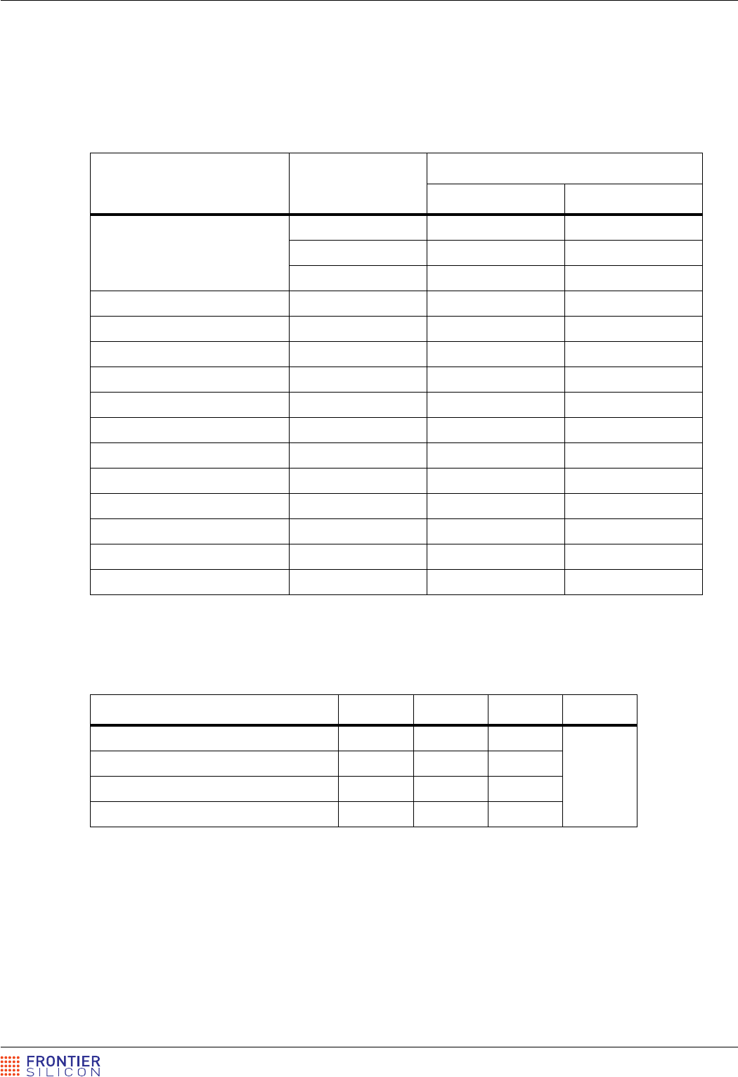
Parameter Min Typ Max Comments Units
Total standby power - - 1 Complies with Eco
certification
W
5 V power terminal 0 5 5.5 V
3.3 V power terminal 0 3.3 3.63
1.2 V power terminal 0 1.2 1.32
VIN 1.17 - 3.3V Other than supply pins
Storage temperature -40 - +85 °C
Operating temperature 0 - +60
Humidity 0 - 90 Non-condensing %
RF input - +10 dBm
Other inputs -0.3 - 3.6 V
Outputs -20 - +20 mA
Table 24: Absolute maximum ratings
Parameter Min Typ Max Units
5V power terminal 4.75 5 5.25 V
3.3V power terminal 3.135 3.3 3.316
1.2V power terminal 1.14 1.2 1.26
Table 25: Operating conditions
FSM 0002 8613 Rev 3 33/41
Venice 8 CONFIDENTIAL NDA 8 Electrical specifications
8.3 Typical power consumption
Table 26 shows typical power consumption at a temperature of 25 °C. This includes GPIO driving
current to the display, but not the display backlight, the current for which is supplied externally to the
module.
8.4 Main signal levels
Operating Mode Supply Voltage Supply Current (mA)
Typical Maximum
DAB only 5.0V 0 5
3.3V 197 230
1.2V 97 130
Soft FM only 5.0V 0 5
3.3V 203 230
1.2V 95 130
Wi-Fi Internet radio 5.0V 1 5
3.3V 390 450
1.2V 105 140
Ethernet Internet radio 5.0V 112 130
3.3V 194 230
1.2V 106 130
iPod play back 5.0V 0 5
3.3V 146 180
1.2V 89 120
Table 26: Typical power consumption
Parameter Min Typ Max Units
LOW level input voltage - - 0.8 V
HIGH level input voltage 2 - -
Schmitt trigger low-to-high threshold 1.67 1.73 1.79
Schmitt trigger high-to-low threshold 1.01 1.07 1.15
Table 27: Main signal levels

34/41 FSM 0002 8613 Rev 3
Datasheet CONFIDENTIAL NDA Venice 8
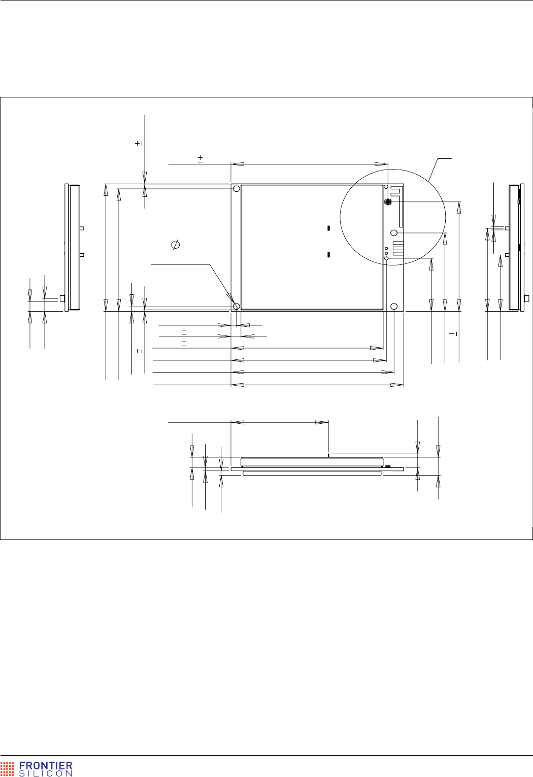
9 Mechanical specification
Reflecting the fact that Venice 8 is designed for a completely new kind of connected audio device,
the module has a new form factor 65 x 80 mm, and is not backwards-compatible with previous
Frontier Silicon radio modules.
9.1 Physical specification
Venice 8 is a single-sided assembly built with a 8-layer printed circuit board. The RF and
baseband circuitry are shielded to meet EMC and RF performance specifications. The shielding
separates the RF and baseband sections.
The mating connector for Venice 8 is:
Manufacturer: Samtec
Description: Con PLG 100 way (50 x 2) pin header vertical 1.27 SMT
Part number: REF-146673-01
FSM 0002 8613 Rev 3 35/41
Venice 8 CONFIDENTIAL NDA 9 Mechanical specification
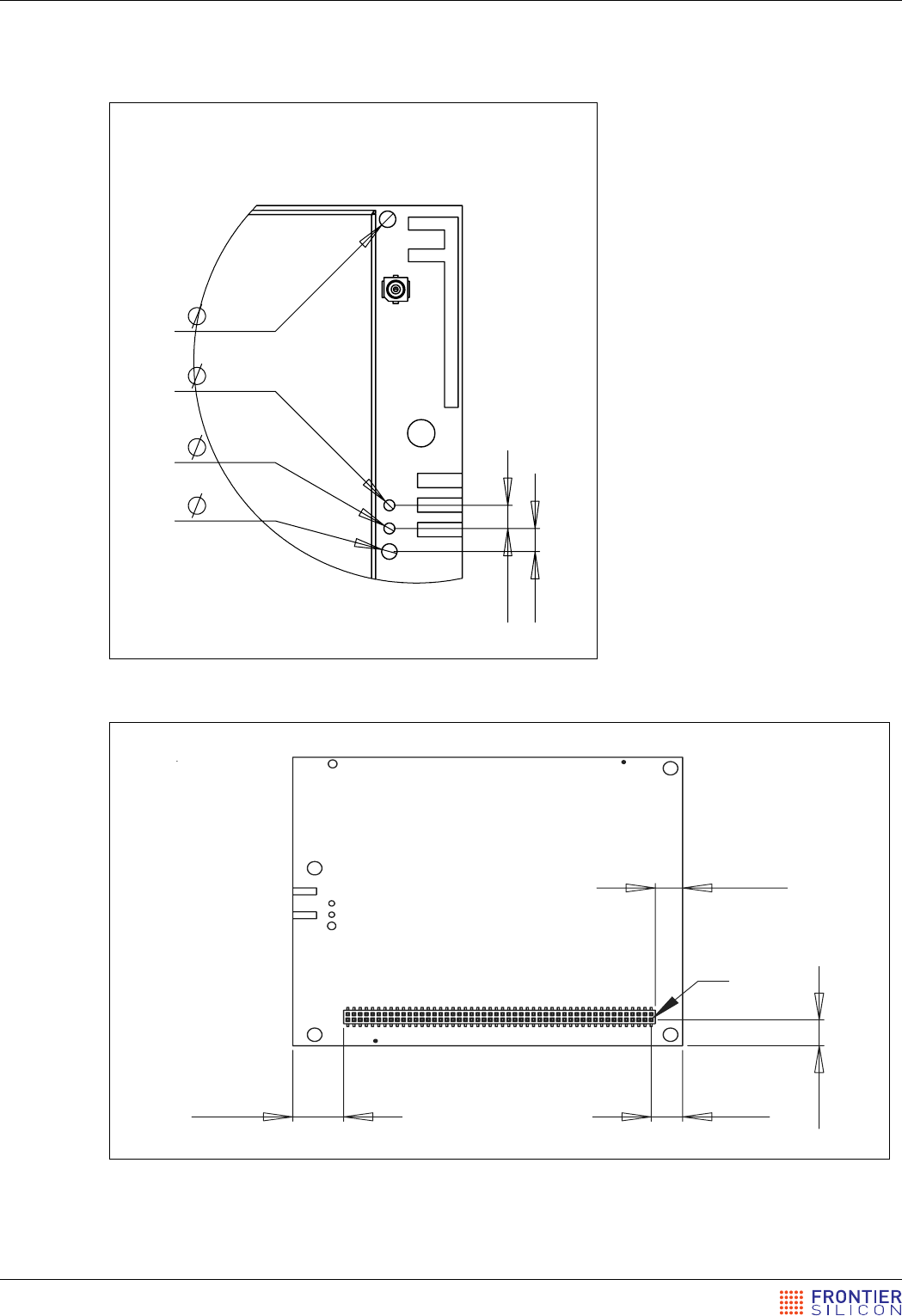
9.2 Physical layout
The following diagrams show the placement of the major components when viewed from the top
and the dimensions in mm.
Figure 5: Module top and side dimensions
80
3
4 Places
4.6
0.25
2.5
72
75.5
27
40
55.8
0.5
72.7
0.5
65
2.5
62.5
0.6
0.25
0.6
0.25
70.5 0.25
A
4.98
6.5
1.60
28.7
42.3
9.15
2.25
1.6
5.3
7.1
45.2

FSM 0002 8613 Rev 3 37/41
Venice 8 CONFIDENTIAL NDA 10 Compliance standards
10 Compliance standards
Venice 8 is designed to allow customers’ finished products to gain compliance with the following
certifications:
CE,
Wi-Fi Alliance,
DLNA 1.5,
WWi,
MFi,
FCC.
10.1 Electromagnetic compatibility (EMC)
Venice 8 is tested in configurations representative of typical DAB consumer products to the
following standards:
BS EN 55013: 2001 for emissions,
BS EN 55020: 2002 for immunity.
The electromagnetic compatibility of a particular product is dependent upon the use and
installation of the module within the product. Care should be taken to integrate the module with
due regard to the effects of conducted and radiated signals.
10.2 Electrostatic discharge (ESD) protection
Venice 8 is an ESD-sensitive device. It is tested to the standard EN61000 (4 kV on RF inputs).
Special handling precautions should be used during manufacturing and testing.
10.3 Restriction of hazardous substances (RoHS)
All Frontier Silicon products meet the requirements of the EU RoHS directive 2002/95/EC RoHS,
use RoHS-certified components and are assembled using lead-free processes. See the Frontier
Silicon Declaration of Materials Compliance [reference 2].
Additionally, Frontier Silicon adheres to best industry practice regarding the avoidance of
environmentally harmful substances in products, above and beyond legal requirements such as
RoHS.

38/41 FSM 0002 8613 Rev 3
Datasheet CONFIDENTIAL NDA Venice 8
10.4 FCC statement
The Venice 8 module is conformant with FCC standards under the "modular approval" only. The
FCC ID for the Venice 8 module is YYX-HA-FS2028-F.
10.4.1 Caution: Exposure to radio frequency radiation
The device is compliant to FCC standards in terms of radiated signal levels. Nevertheless, the
device shall be used in such manner that proximity and the potential for human contact with the
radiating antenna, during normal operation, is minimised.
In order to avoid the possibility of exceeding the FCC radio frequency exposure limits, human
proximity to the antenna shall not be less than 20cm (8 inches) during normal operation.
See the Venice 8 Application Note for further information.
10.4.2 Federal Communications Commission notice
This equipment has been tested and found to comply with the limits for a Class B digital device,
pursuant to Part 15 of the FCC Rules. These limits are designed to provide reasonable protection
against harmful interference in a residential installation.
This equipment generates, uses, and can radiate radio frequency energy. If not installed and
used in accordance with the instructions, it may cause harmful interference to radio or television
reception, which can be determined by turning the equipment off and on, in which case the user
is encouraged to try and correct the interference by increasing the distance between the
equipment and the receiver.
10.4.3 Modifications
The FCC requires the user to be notified that any changes or modifications to this device that are
not expressly approved by Frontier Silicon Limited may void the user’s authority to operate the
equipment. Such modifications also invalidate FCC approval of the device.
DECLARATION OF CONFORMITY WITH FCC RULES FOR ELECTROMAGNETIC COMPATIBILITY
Frontier Silicon Limited declares under its sole responsibility that the product FCC-ID: YYX-
HA-FS2028-F, to which this declaration relates, complies with Part 15 of the FCC Rules in
WiFi operating mode only.
It is the responsibility of the final product manufacturer to achieve conformance with Part 15
of the FCC rules for all other operating modes, in the final application. The Venice 8 module
is compliant with Part 15 of the FCC Rules in WiFi, DAB, FM and Ethernet modes in Frontier
Silicon's reference platform Jupiter 8.
Operation is subject to the following two conditions:
(1) This device may not cause harmful interference, and
(2) this device must accept any interference received, including interference that may cause
undesired operation.
The manufacturer of the final product containing the Venice 8 module must ensure that the
product includes an exterior label with the following wording: "Contains FCC ID: YYX-HA-
FS2028-F".

FSM 0002 8613 Rev 3 39/41
Venice 8 CONFIDENTIAL NDA 10 Compliance standards
10.5 RF exposure
10.5.1 Occupational exposure levels
The Venice 8 module meets the Occupational Exposure Levels described in the ICNIRP
Guidelines, FCC 47 CFR § 1.1310 Guidelines, Health Canada’s RF exposure guideline Safety Code
6 and the Australian ARPANSA limits at 20.0cm, the point of investigation.
10.5.2 General public exposure levels
The Venice 8 module meets the General Public Exposure Levels described in the ICNIRP
Guidelines, FCC 47 CFR § 1.1310 Guidelines, Health Canada’s RF exposure guideline Safety Code
6 and the Australian ARPANSA limits at 20.0cm, the point of investigation.

40/41 FSM 0002 8613 Rev 3
Datasheet CONFIDENTIAL NDA Venice 8
Glossary
DAB Digital Audio Broadcasting
FM Frequency Modulation
GPIO General Purpose Input/Output
IC Integrated Circuit
RDS (FM) Radio Data System
SCP Serial Control Protocol
SPI Serial Peripheral Interface
SPI master Provides SPI clock and initiates data transactions and requests
SPI slave Receives SPI clock and responds to data transactions and requests
S/PDIF Sony/Philips Digital Interface
SRAM Static Random Access Memory
TFT Thin Film Transistor [display]
UART Universal Asynchronous Receiver Transmitter
USB Universal Serial Bus
WWi Works With iPhone

41/39 FSM 0002 8613 Rev 3
Datasheet CONFIDENTIAL NDA Venice 8