Fuji Film 02100003 IEEE802.11 b/g/n Wireless LAN module User Manual module
Fuji Film Corporation IEEE802.11 b/g/n Wireless LAN module module
Contents
- 1. User Manual (module)
- 2. User Manual (system)
User Manual (module)

[ ]
All rights are reserved by USI. No part of this technical document can be reproduced in any form without permission of USI
.
1
Data Sheet
Of
WM-N-BM -02_D WLAN
Data Sheet Sep 7 2012 Rev 1.0
802.11b/g/n (WM-N-BM -02_D)
www.usi.com.tw

802.11b/g/n Wireless LAN Daughter board V1.0
All rights are reserved by USI. No part of this technical document can be reproduced in any form without permission of USI
.
2
Introduction
This daughter card featured with full function of
802.11b/g/n
(draft n)
including both H380A and L330W.
This multi- functionality via 21 pins FPC to connect and
provides SDIO/SPI/ (option) interface for WiFi.
The small size & low profile physical design make it
easier for system design to enable high performance
wireless connectiv
ity without space constrain. The low
power consumption and excellent radio performance
make it the best solution for OEM customers who
require embedded 802.11b/g/n Wi-
Fi features, such as,
Wireless PDA, Smart phone, MP3, PMP, slim type
Notebook, VoIP phone etc.
The card
is based on Broadcom 43362 chipset which is
a WiFi Transceiver SOC. The Radio architecture & high
integration MAC/BB chip provide excellent sensitivity
with rich system performance. The
card is designed as
single antenna for WiFi for the application of small size
hand held device.
In addition to WEP 64/128, WPA and TKIP, AES, CCX
is supported to provide the latest security requirement
on your network.
For the software and driver development, USI provides
extensive technical document and reference software
code for the system integration under the agreement of
Broadcom International Ltd.
Hardware evaluation kit and development utilities will
be released base on listed OS and processors to OEM
customers.
Features
Lead Free design which supporting Green
design requirement, RoHS Compliance.
Small size suitable for low volume system
integration.
Low power consumption & excellent power
management performance extend battery
life.
2.412-2.484 GHz two SKUs for worldwide
market.
Easy for i
ntegration into mobile and handheld
device with flexible system configuration and
antenna design.
Supports per packet Rx Antenna diversity

802.11b/g/n Wireless LAN Daughter board V1.0
All rights are reserved by USI. No part of this technical document can be reproduced in any form without permission of USI
.
3
Change Sheet
Rev.
Date
Description of change
Approval & Date
Page Par Change(s)
1.0
09/07/12
All All Draft version for Review

802.11b/g/n Wireless LAN Daughter board V1.0
All rights are reserved by USI. No part of this technical document can be reproduced in any form without permission of USI
.
4
TABLE OF CONTENTS
Introduction ............................................................................................................................................. 2
Features .................................................................................................................................................... 2
1. EXECUTIVE SUMMARY ................................................................................................................ 5
2. BLOCK DIAGRAM .......................................................................................................................... 6
3. DELIVERABLES ............................................................................................................................. 7
4. REFERENCE DOCUMENTS ......................................................................................................... 8
5. TECHNICAL SPECIFICATION ..................................................................................................... 9
5.1.
ABSOLUTE MAXIMUM RATING ............................................................................................ 9
5.2.
RECOMMENDABLE OPERATION CONDITION .................................................................... 9
5.2.1.
TEMPERATURE, HUMIDITY ......................................................................................... 9
5.2.2.
VOLTAGE ...................................................................................................................... 9
5.2.3.
POWER CONSUMPTION (SDIO, GSPI MODE) ............................................................ 9
5.3.
WIRELESS SPECIFICATIONS ............................................................................................ 10
5.4.
RADIO SPECIFICATIONS 802.11B/G/N .............................................................................. 10
5.5.
ANTNENNA SPECIFICATIONS ........................................................................................... 11
5.6.
REFERENCE CIRCUIT ........................................................................................................ 12
5.7.
TIMING DIAGRAM OF INTEFACE ....................................................................................... 13
5.8.
DIMENSIONS, WEIGHT AND MOUNTING .......................................................................... 17
5.8.1.
DIMENSIONS ............................................................................................................... 17
6. LEGAL, REGULATORY & OTHER TECHNICAL CONSTRAINTS ..................................... 18
7. PIN OUT AND PIN DESCRIPTION ............................................................................................ 18
8. PACKAGE AND STORAGE CONDITION.................................................................................... 20
8.1.
PACKAGE DIMENSION ....................................................................................................... 20
8.2.
ESD LEVEL ......................................................................................................................... 20

802.11b/g/n Wireless LAN Daughter board V1.0
All rights are reserved by USI. No part of this technical document can be reproduced in any form without permission of USI
.
5
1. EXECUTIVE SUMMARY
The WM-N-BM -02_D is one of the product families in UG’s product offering, targeting for system
integration requiring a smaller form factor. It also provides the standard migration to high data rate
to UG’s current SIP customers.
The purpose of this document is to define the product specification for 802.11b/g/n (draft n) WiFi WM-
N-BM -02_D. All the data in this document is based on Broadcom 43362 data sheet and other
documents provided from Broadcom. The data will be updated after implementing the
measurement of the .
This product is designated for use in embedded applications mainly in the mobile device, which
required small size and high data rate wireless connectivity. The application such as, Wireless
PDA, slim type Notebook, Media Adapter, Barcode scanner, mini-Printer, VoIP phone, Data
storage device could be the potential application for wireless WM-N-BM -02_D.
802.11b/g/n Wireless LAN Daughter board V1.0
All rights are reserved by USI. No part of this technical document can be reproduced in any form without permission of USI
.
6
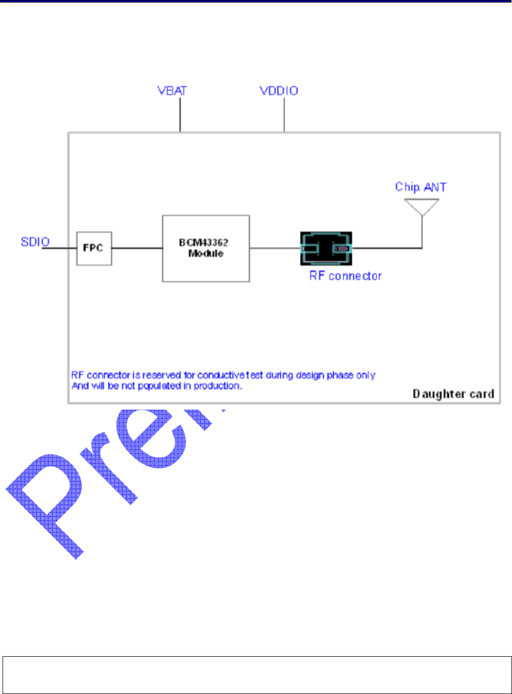
2. BLOCK DIAGRAM
The WM-N-BM -02_D is designed based on Broadcom 43362 chipset solution.
It supports generic SPI (G-SPI), SDIO interface to connect the WLAN to the host processor.
A simplified block diagram of the WM-N-BM -02_D is depicted in the Fig. below.
WM-N-BM -02_D
\

802.11b/g/n Wireless LAN Daughter board V1.0
All rights are reserved by USI. No part of this technical document can be reproduced in any form without permission of USI
.
7
3. DELIVERABLES
The following products and software will be part of the product.
• WM-N-BM -02_D with packaging
• Evaluation kits (with SDIO / SPI interface)
• Software utility which supporting customer for integration, performance test and
homologation. Capable of testing, loading (firmware) and configuring (MAC, CIS) for the
WM-N-BM -02_D .
• Unit Test / Qualification report
• Product Specifications.
• Agency certification pre-test report base on adapter boards

802.11b/g/n Wireless LAN Daughter board V1.0
All rights are reserved by USI. No part of this technical document can be reproduced in any form without permission of USI
.
8
4. REFERENCE DOCUMENTS
C.I.S.P.R.
Pub. 22
"Limits and methods of measurement of radio interference
characteristics of information technology equipment." International
Special Committee on Radio Interference (C.I.S.P.R.), Third Edition,
1997.
CB Bulletin
No. 96A
"Adherence to IEC Standards: “Requirements for IEC 950, 2
nd
Edition
and Amendments 1 (1991), 2(1993), 3 (1995) and 4(1996). Product
Categories: Meas, Med, Off, Tron." IEC System for Conformity Testing
to Standards for Safety of Electrical Equipment (IECEE), April 2000.
CFR 47,
Part 15-B
"Unintentional Radiators". Title 47 of the Code of Federal Regulations,
Part 15, FCC Rules, Radio Frequency Devices, Subpart B.
CFR 47,
Part 15-C
"Intentional Radiators". Title 47 of the Code of Federal Regulations,
Part 15, FCC Rules, Subpart C. URL:
http://www.access.gpo.gov/nara/cfr/waisidx_98/47cfr15_98.html
CSA C22.2
No. 950-95
"Safety of Information Technology Equipment including Electrical
Business Equipment, Third Edition." Canadian Standards Association,
1995, including revised pages through July 1997.
EN 60 950 "Safety of Information Technology Equipment Including Electrical
Business Equipment." European Committee for Electrotechnical
Standardization (CENELEC), 1996, (IEC 950, Second Edition, including
Amendment 1, 2, 3 and 4).
IEC 950 "Safety of Information Technology Equipment Including Electrical
Business Equipment." European Committee for Electrotechnical
Standardization, Intentional Electrotechnical Commission. 1991, Second
Edition, including Amendments 1, 2, 3, and 4.
IEEE 802.11 “Wireless LAN Medium Access Control (MAC) And Physical Layer (PHY)
Specifications.” Institute of Electrical and Electronics Engineers. 1999.

802.11b/g/n Wireless LAN Daughter board V1.0
All rights are reserved by USI. No part of this technical document can be reproduced in any form without permission of USI
.
9
5. TECHNICAL SPECIFICATION
5.1. ABSOLUTE MAXIMUM RATING
Supply Power Max +3.6 Volt
Non Operating Temperature
- 40° to 85° Celsius
Voltage ripple +/- 2% Max. Values not exceeding Operating
voltage
5.2. RECOMMENDABLE OPERATION CONDITION
5.2.1. TEMPERATURE, HUMIDITY
The WM-N-BM -02_D has to withstand the operational requirements as listed in the table
below.
Operating Temperature -20° to 65° Celsius for SDIO/gSPI version
Humidity range Max 95% Non condensing, relative humidity
5.2.2. VOLTAGE
Power supply for the WM-N-BM -02_D will be provided by the host via the power pins
Symbol Parameter Min Typ Max Unit
VBAT 3.3V Power Supply 2.8 3.3 5.0 V
VDDIO Host Interface Power Supply 1.62 1.8 1.98 V
2.97 3.3 3.63 V
5.2.3. POWER CONSUMPTION (SDIO, GSPI MODE)
a. For 1Mbps Max. current
b. For 6Mbps and 11n HT20 MCS0 Max. current
c. Include USB mode and SDIO mode max .current range
Include EVB power consumption
Power consumption Typical
Max
WiFi
Tx @ 17dBm output power @ 25C (11b), 3.3V 350mA
Tx @ 15dBm output power @ 25C (11g), 3.3V 310mA
Tx @ 15dBm output power @ 25C (11n, HT20), 3.3V 310mA
Rx @25C, 3.3V
130mA

802.11b/g/n Wireless LAN Daughter board V1.0
All rights are reserved by USI. No part of this technical document can be reproduced in any form without permission of USI
.
10
5.3. WIRELESS SPECIFICATIONS
The WM-N-BM -02_D complies with the following features and standards;
Features
Description
WLAN Standards
IEEE 802 Part 11b/g/n (802.11b/g/n)
Antenna Port
Support Single Antenna for WiFi
Frequency Band 2.412 GHz – 2.484 GHz
5.4. RADIO SPECIFICATIONS 802.11B/G/N
Features
Description
Frequency Band 2.4000 GHz – 2.484 GHz (2.4 GHz ISM Band)
Number of selectable Sub
channels 14 channels
Modulation OFDM, DSSS (Direct Sequence Spread Spectrum),
DBPSK, DQPSK, CCK , 16QAM, 64QAM
Supported rates 1,2, 5.5,11,6,9,12,24,36,48,54 Mbps
Maximum receive level -10dBm (with PER < 8%)
Output Power
17 dBm +2/
-
2 dBm for 1, 2, 5.5, 11Mbps
14 dBm +2/-2 dBm for
6, 9, 12, 18, 24, 36, 48, 54 Mbps
12 dBm +2/-2 dBm for 11n (HT20)
EVM
Typical
Maximum
Unit
@11 Mbps
-
13
-
11
dB
@1 Mbps
-
13
-
11
dB
@54 Mbps
-
30
-
25
dB
@6 Mbps
-
30
-
22
dB
HT20 @ MCS0
-
30
-
22
dB
HT20 @ MCS7
-
30
-
28
dB
Receiver Characteristics ( 3.3V, 25 degree C ) Typical Max. Unit
PER <8%, Rx Sensitivity @ 1 Mbps -91 -88 dBm
PER <8%, Rx Sensitivity @ 11 Mbps -87 -83 dBm
PER <10%
,
Rx Sensitivity @ 6 Mbps -87 -83 dBm
PER <10%, Rx Sensitivity @ 54 Mbps -73 -69 dBm
PER <10%, Rx Sensitivity @ MCS0 -87 -83 dBm
PER <10%, Rx Sensitivity @ MCS7 -70 -66 dBm
Note "All Rx Sensitivity and Tx EVM specifications are reference to BCM43362 module test"
802.11b/g/n Wireless LAN Daughter board V1.0
All rights are reserved by USI. No part of this technical document can be reproduced in any form without permission of USI
.
11
5.5. ANTNENNA SPECIFICATIONS
H380A type:
Diversity Antenna
(Rx Only)
Band Units
2400
Normal Impedance 50 Ohms
Operating Frequency
2412-2484 MHz
VSWR <2:1 -
Radiated Efficiency
1
30 %
Peak Gain
1,2
TBD dBi
Directivitity
1,3
TBD dBi
1
For reference only. Active measurements are the only requirement.
2
Peak gain measured with 0dBm reference input.
3
Directivity(dBi) = Peak Gain(dB) – Average Gain(dB)
4
Band 850 fully covers CDMA 800 (BC0)
L330W type:
Diversity Antenna
(Rx Only)
Band
Units
2400
Normal Impedance 50 Ohms
Operating Frequency
2412
-
2484
MHz
VSWR
<2:1
-
Radiated Efficiency
1
40 %
Peak Gain
1,2
TBD
dBi
Directivitity
1,3
TBD
dBi
1
For reference only. Active measurements are the only requirement.
2
Peak gain measured with 0dBm reference input.
3
Directivity(dBi) = Peak Gain(dB) – Average Gain(dB)
4
Band 850 fully covers CDMA 800 (BC0)
802.11b/g/n Wireless LAN Daughter board V1.0
All rights are reserved by USI. No part of this technical document can be reproduced in any form without permission of USI
.
12
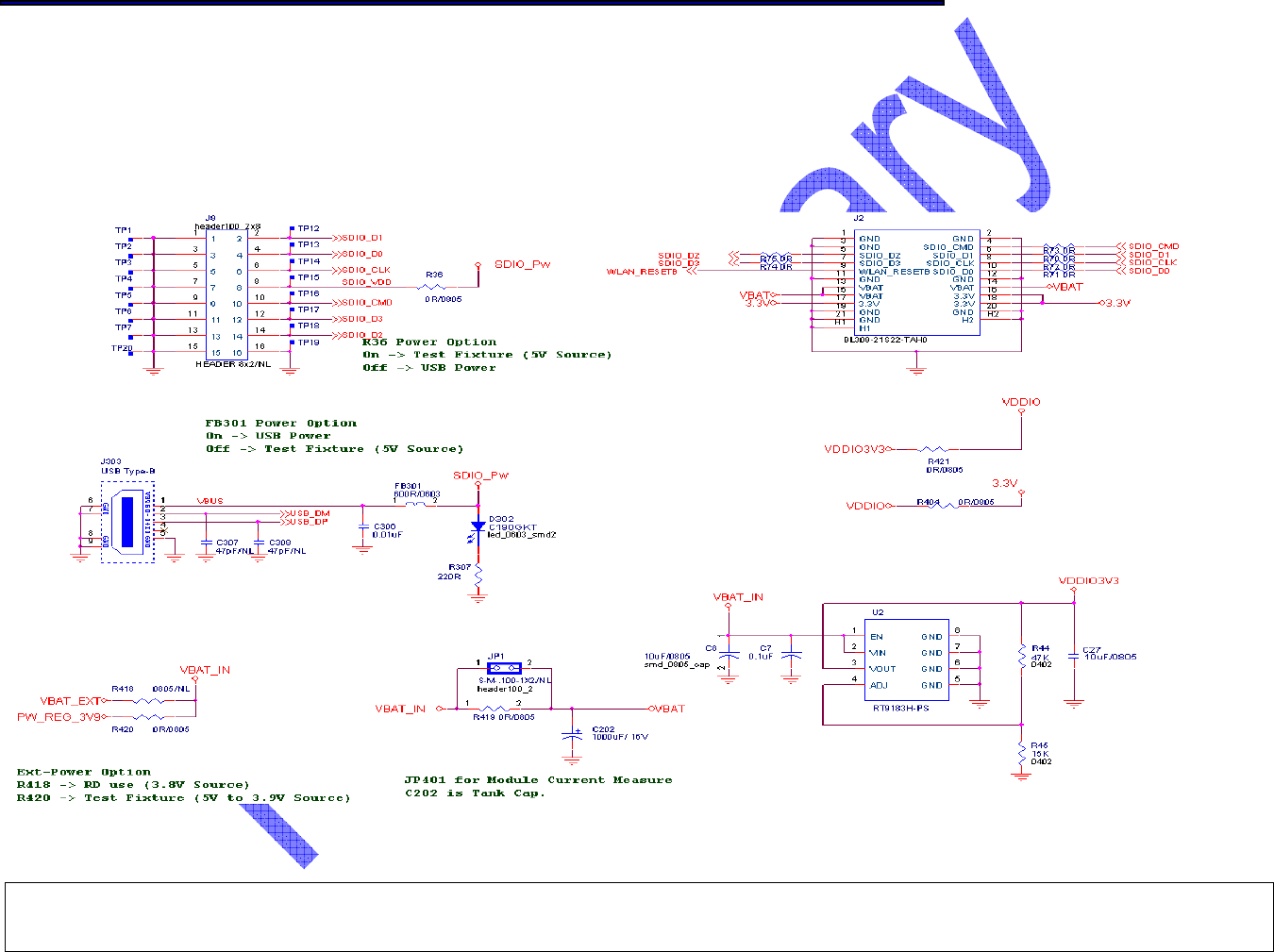
5.6. REFERENCE CIRCUIT
802.11b/g/n Wireless LAN Daughter board V1.0
All rights are reserved by USI. No part of this technical document can be reproduced in any form without permission of USI
.
13
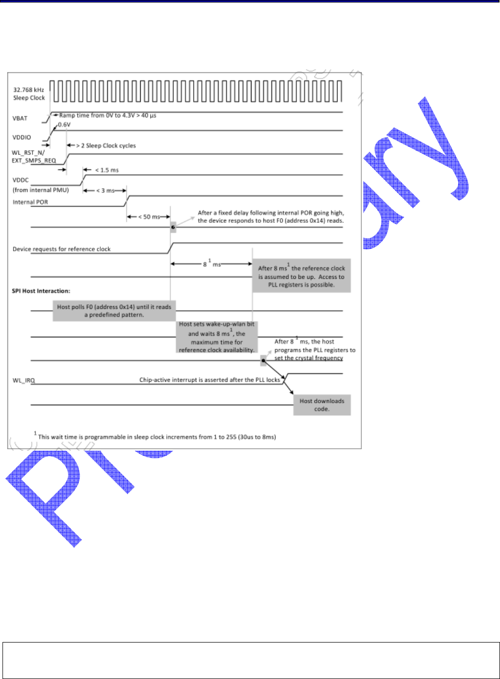
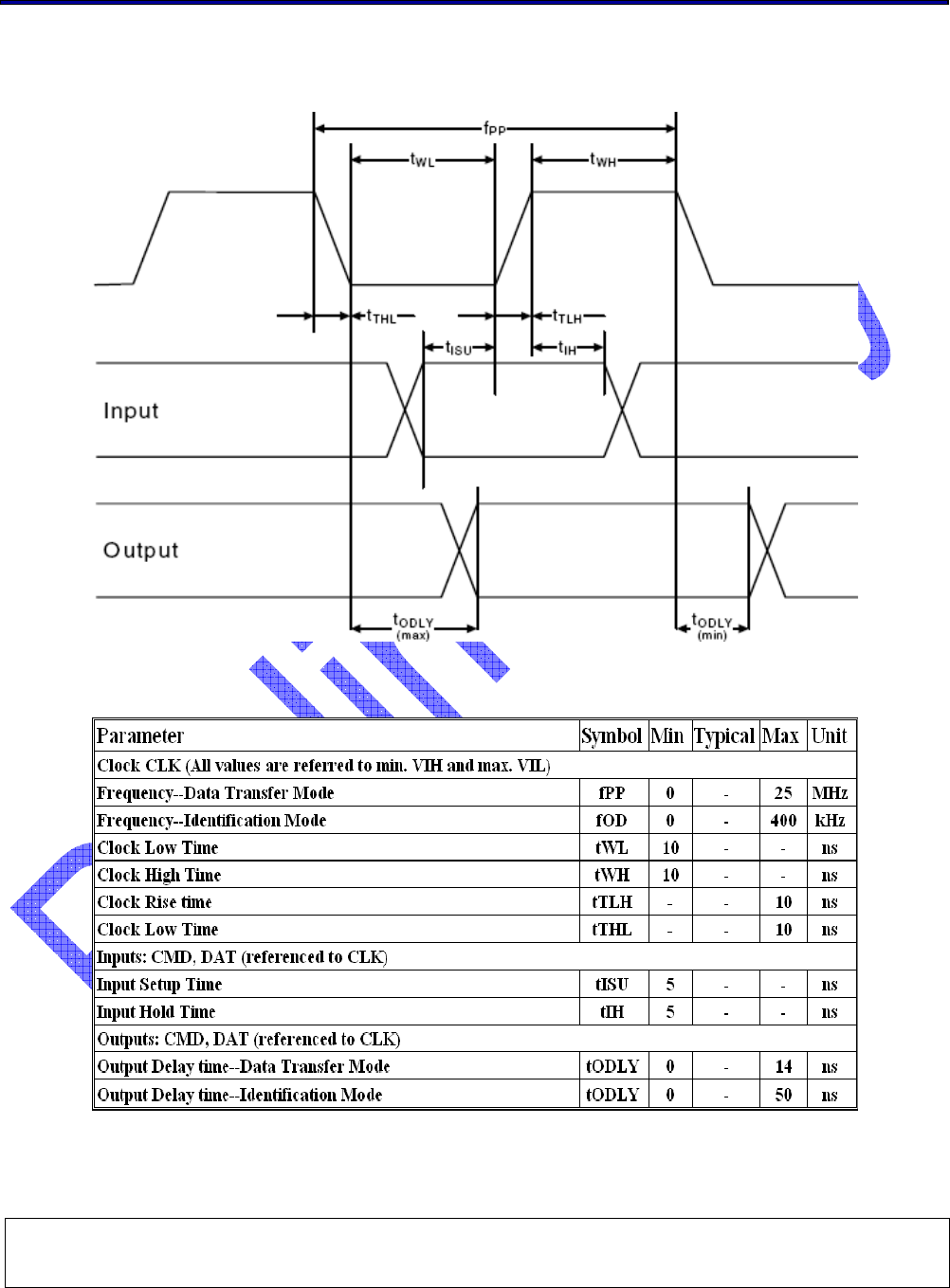
5.7. TIMING DIAGRAM OF INTEFACE
WIFI BOOT-UP Sequence
WIFI BOOT-UP Sequence
802.11b/g/n Wireless LAN Daughter board V1.0
All rights are reserved by USI. No part of this technical document can be reproduced in any form without permission of USI
.
14
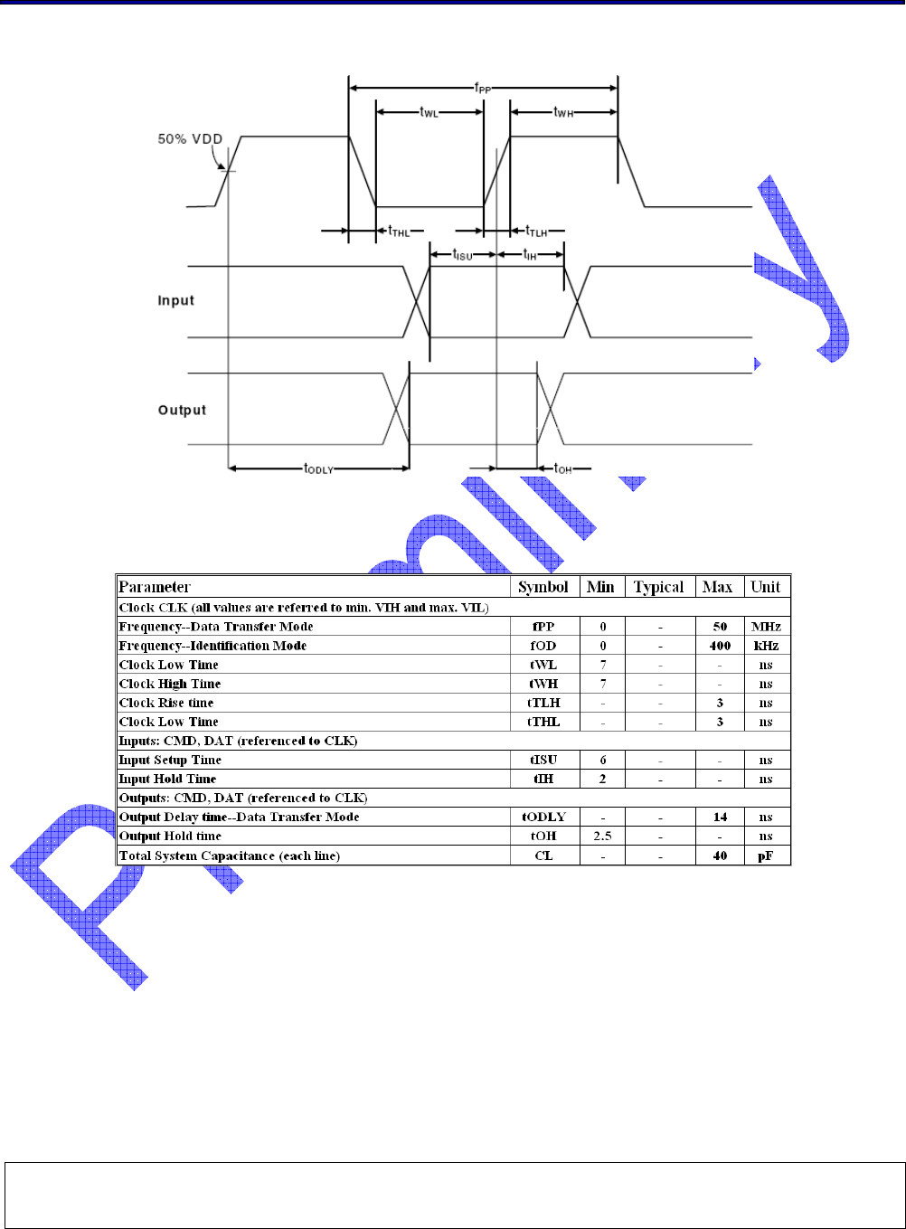
SDIO TIMING
SDIO timing in default mode
SDIO Bus Timing Parameters (Default Mode)
802.11b/g/n Wireless LAN Daughter board V1.0
All rights are reserved by USI. No part of this technical document can be reproduced in any form without permission of USI
.
15
SDIO timing in High-Speed Mode
SDIO Bus Timing Parameters (High-Speed Mode)
802.11b/g/n Wireless LAN Daughter board V1.0
All rights are reserved by USI. No part of this technical document can be reproduced in any form without permission of USI
.
16
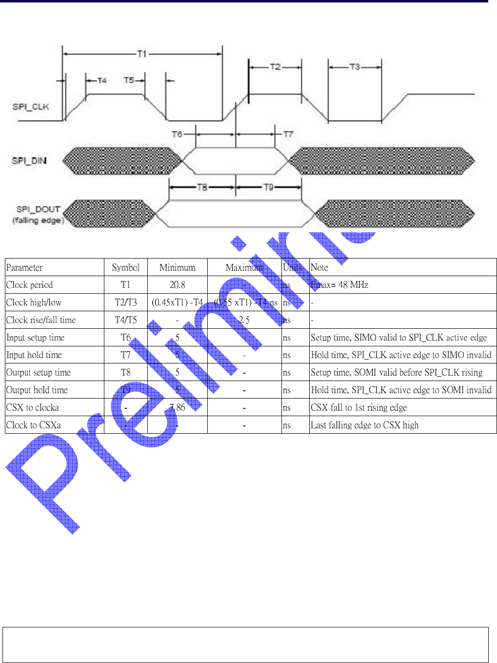
GSPI Timing
a.SPI_CSx remains active for entire duration of SPI read/write/write_read transaction (i.e., overall
words for multiple word transaction)
Interface during Sleep mode
PD: Pull Down, PU: Pull UP
802.11b/g/n Wireless LAN Daughter board V1.0
All rights are reserved by USI. No part of this technical document can be reproduced in any form without permission of USI
.
17
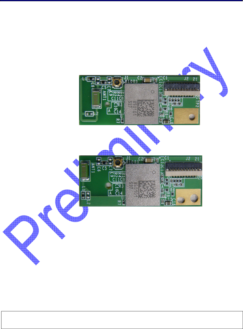
5.8. DIMENSIONS, WEIGHT AND MOUNTING
The following paragraphs provide the requirements for the size, weight and mounting of the
WM-N-BM -02_D .
5.8.1. DIMENSIONS
The size and thickness of the WM-N-BM -02_D is “11 mm (W) x 27 mm (L) x 1.8 mm (Max)(H)
H380A
L330W
802.11b/g/n Wireless LAN Daughter board V1.0
All rights are reserved by USI. No part of this technical document can be reproduced in any form without permission of USI
.
18
6. LEGAL, REGULATORY & OTHER TECHNICAL CONSTRAINTS
The WM-N-BM -02_D is pre-tested to ensure that all requirements met as set forth in the
following sections.
Final certification ( certification) requires the antenna of targeted system with a lead-time of 6
weeks. The product deliverable shall be a pre-tested WM-N-BM -02_D . No level certification
on WM-N-BM -02_D .
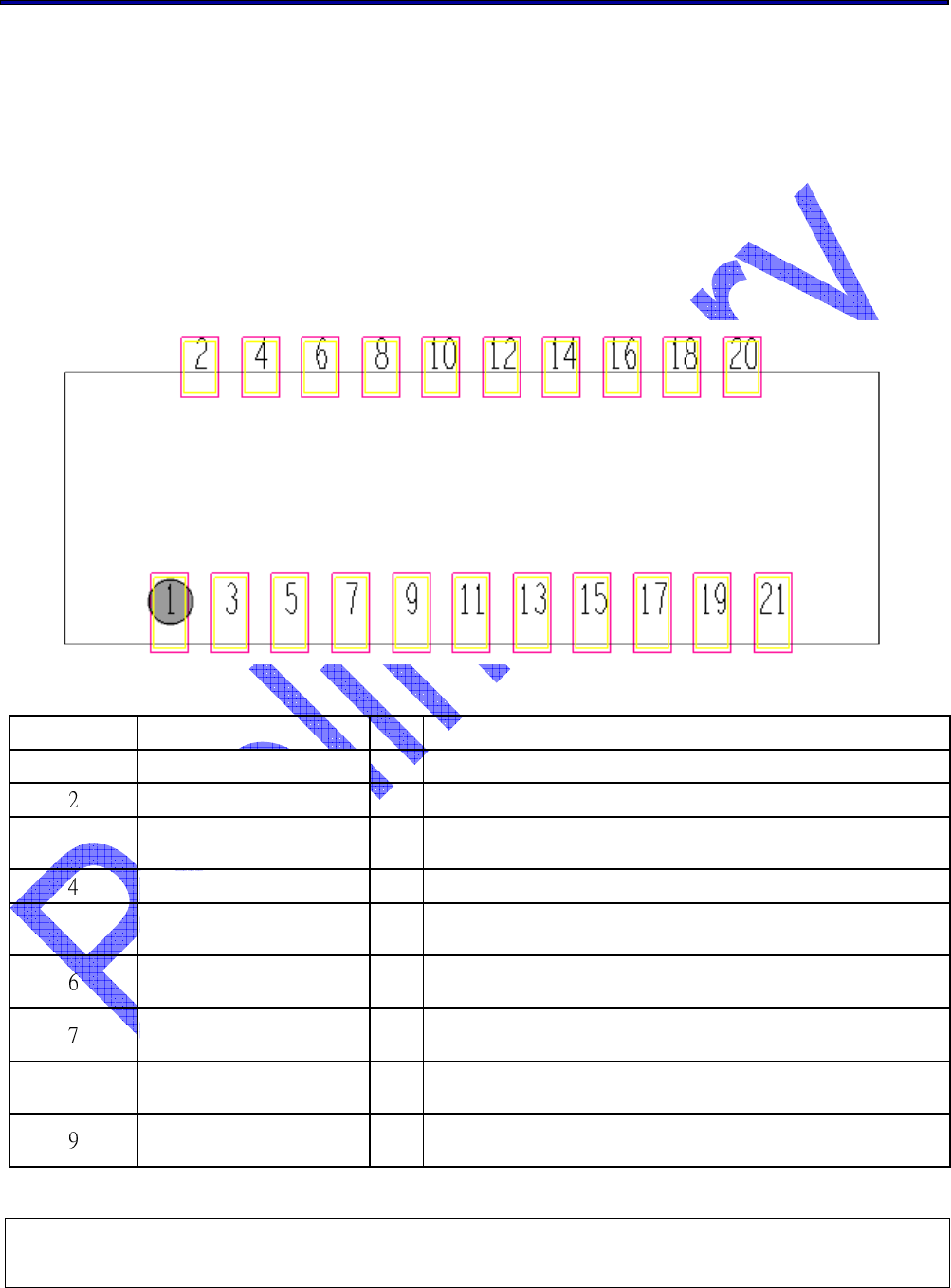
7. PIN OUT AND PIN DESCRIPTION
Top View
Pin Description
Pin-Nmnber
Pin-Define Type
Description
1 GND I Ground
GND I Ground
3 SDIO_CLK I/O
SDIO clock. This pin has an internal weak pull-up
resistor.
GND I Ground
5 SDIO_DAT0 I/O
SDIO data 0. This pin has an internal weak pull-up
resistor.
SDIO_CMD I/O
SDIO command. This pin has an internal weak pull-up
resistor.
SDIO_DAT3 I/O
SDIO data 3. This pin has an internal weak pull-up
resistor.
8 SDIO_DAT2 I/O
SDIO data 2. This pin has an internal weak pull-up
resistor.
SDIO_DAT1 I/O
SDIO data 1. This pin has an internal weak pull-up
resistor.
802.11b/g/n Wireless LAN Daughter board V1.0
All rights are reserved by USI. No part of this technical document can be reproduced in any form without permission of USI
.
19
10 WLAN_RESETB I
Active low WLAN reset signal includes an internal
200K
Ω
pull-down resistor. Within 1.5ms of WL_RST_N
being driven high, the PMU changes this from PD to
High-Z, Software can optionally enable the pull-down
resistor. VIH=1.08V to 3.6V. VIL<0.4V
GND I Ground
GND I Ground
GND I Ground
VBAT I Battery supply input (2.8V~5V)
VBAT I Battery supply input (2.8V~5V)
VBAT I Battery supply input (2.8V~5V)
3.3V I --Digital I/O supply ( 3.3V)
3.3V I --Digital I/O supply (3.3V)
3.3V I --Digital I/O supply (3.3V)
GND I Ground
GND I Ground
802.11b/g/n Wireless LAN Daughter board V1.0
All rights are reserved by USI. No part of this technical document can be reproduced in any form without permission of USI
.
20
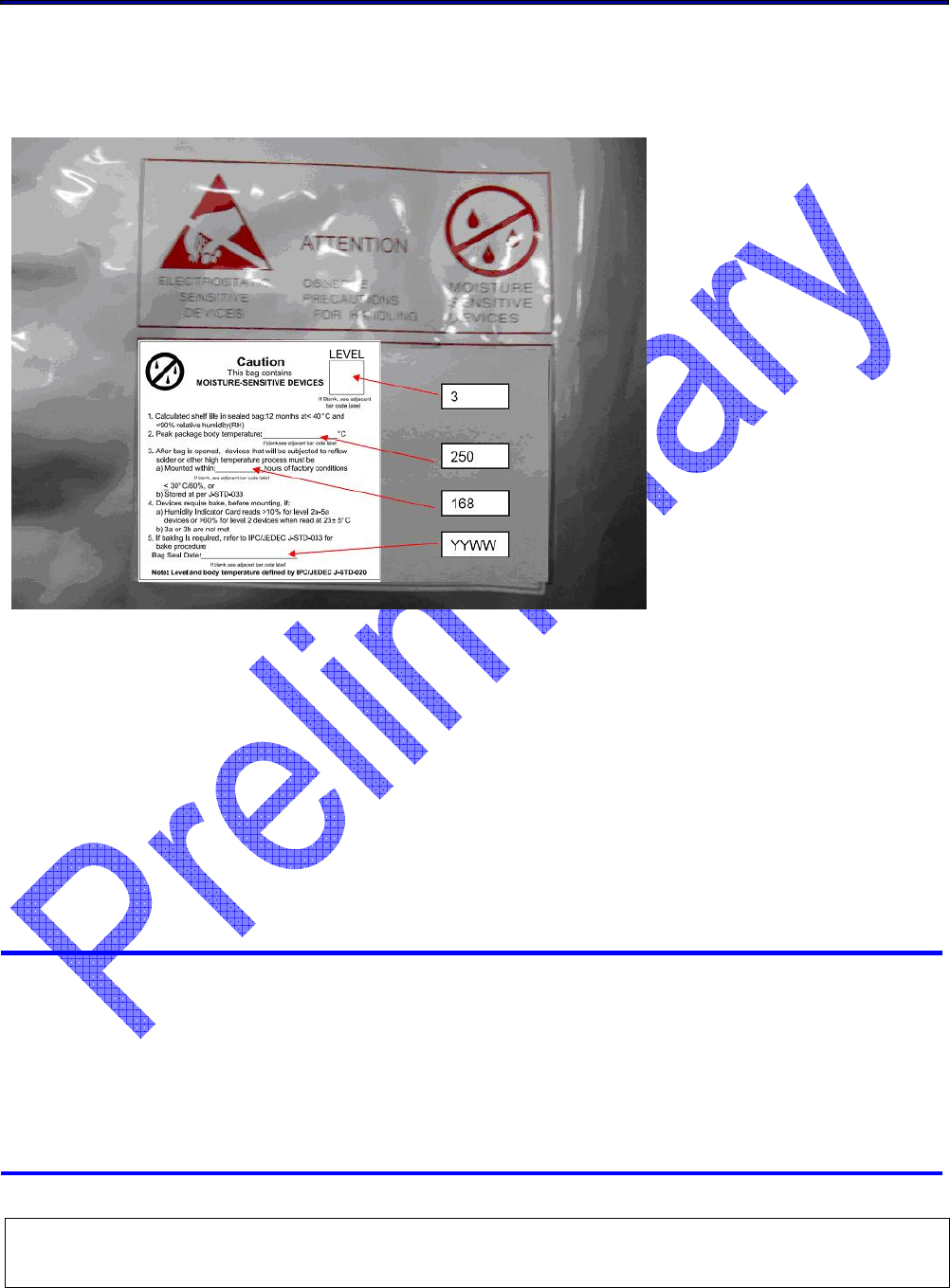
8. PACKAGE AND STORAGE CONDITION
8.1. PACKAGE DIMENSION
8.2. ESD LEVEL
For Additional information, please contact the following:
Universal Scientific Industrial Co., Ltd.
Headquarters
141, Lane 351, Taiping Road, Sec. 1, Tsao-Tuen, Taiwan,
Http://www.usi.com.tw
Tel: + 886-49-2350876, 2325876
Fax: +886-49-3439561, 2337360,2351093
E-mail:usi@ms.usi.com.tw
Federal Communication Commission Interference Statement
This device complies with Part 15 of the FCC Rules. Operation is subject to the
following two conditions: (1) This device may not cause harmful interference, and
(2) this device must accept any interference received, including interference that may
cause undesired operation.
This equipment has been tested and found to comply with the limits for a Class B
digital device, pursuant to Part 15 of the FCC Rules. These limits are designed to
provide reasonable protection against harmful interference in a residential installation.
This equipment generates, uses and can radiate radio frequency energy and, if not
installed and used in accordance with the instructions, may cause harmful interference
to radio communications. However, there is no guarantee that interference will not
occur in a particular installation. If this equipment does cause harmful interference to
radio or television reception, which can be determined by turning the equipment off
and on, the user is encouraged to try to correct the interference by one of the
following measures:
- Reorient or relocate the receiving antenna.
- Increase the separation between the equipment and receiver.
- Connect the equipment into an outlet on a circuit different from that
to which the receiver is connected.
- Consult the dealer or an experienced radio/TV technician for help.
FCC Caution: Any changes or modifications not expressly approved by the party
responsible for compliance could void the user's authority to operate this equipment.
This transmitter must not be co-located or operating in conjunction with any other
antenna or transmitter.

Radiation Exposure Statement:
This equipment complies with FCC radiation exposure limits set forth for an
uncontrolled environment. This module can be used with FUJIFILM Digital
Camera: FinePix S8200W, FinePix S8250W, FinePix S8300W, FinePix S8350W,
FinePix S8400W, FinePix S8450W, FinePix S8500W, FinePix S8550W, FinePix
S8230W, FinePix S8330W, FinePix S8430W, FinePix S8530W or similar platform
with similar dimension, antenna location and RF characteristic.
This device is intended only for OEM integrators under the following conditions:
1) The antenna must be installed at same location as tested in the certification filing.
2) The transmitter module may not be co-located with any other transmitter or
antenna.
3) For portable usage condition, this module has been SAR evaluated in Fuji Film
Digital Camera: FinePix S8200W host with compliance result and can be used
with this specific host as described in the certification filing. Other host or platform
needs separate approval.
As long as 3 conditions above are met, further transmitter test will not be required.
However, the OEM integrator is still responsible for testing their end-product for any
additional compliance requirements required with this module installed
IMPORTANT NOTE: In the event that these conditions can not be met (for example
certain laptop configurations or co-location with another transmitter), then the FCC
authorization is no longer considered valid and the FCC ID can not be used on the
final product. In these circumstances, the OEM integrator will be responsible for
re-evaluating the end product (including the transmitter) and obtaining a separate FCC
authorization.
End Product Labeling
The final end product must be labeled in a visible area with the following: “Contains
FCC ID: W2Z-02100003”. The grantee's FCC ID can be used only when all FCC
compliance requirements are met.
Manual Information To the End User
The OEM integrator has to be aware not to provide information to the end user
regarding how to install or remove this RF module in the user’s manual of the end
product which integrates this module.
The end user manual shall include all required regulatory information/warning as
show in this manual.
IC Regulations:
This device complies with Industry Canada license-exempt RSS standard(s). Operation is subject
to the following two conditions:
(1) this device may not cause interference, and
(2) this device must accept any interference, including interference that may cause undesired
operation of the device.
Le présent appareil est conforme aux CNR d'Industrie Canada applicables aux appareils radio
exempts de licence. L'exploitation est autorisée aux deux conditions suivantes:
(1) l'appareil ne doit pas produire de brouillage, et
(2) l'utilisateur de l'appareil doit accepter tout brouillage radioélectrique subi, même si le
brouillage est susceptible d'en compromettre le fonctionnement."
This Class B digital apparatus complies with Canadian ICES-003.
Cet appareil numérique de la classe B est conforme à la norme NMB-003 du Canada.
IMPORTANT NOTE:
IC Radiation Exposure Statement:
This equipment complies with IC RSS-102 radiation exposure limits set forth for an uncontrolled
environment. This module can be used with FUJIFILM Digital Camera: FinePix S8200W,
FinePix S8250W, FinePix S8300W, FinePix S8350W, FinePix S8400W, FinePix
S8450W, FinePix S8500W, FinePix S8550W, FinePix S8230W, FinePix S8330W,
FinePix S8430W, FinePix S8530W or similar platform with similar dimension, antenna
location and RF characteristic.
This device and its antenna(s) must not be co-located or operating in conjunction with any other
antenna or transmitter.
Under Industry Canada regulations, this radio transmitter may only operate using an antenna of a
type and maximum (or lesser) gain approved for the transmitter by Industry Canada. To reduce
potential radio interference to other users, the antenna type and its gain should be so chosen that
the equivalent isotropically radiated power (e.i.r.p) is not more than necessary for successful
communication.
Conformément à la réglementation d'Industrie Canada, le présent émetteur radio peut fonctionner
avec une antenne d'un type et d'un gain maximal (ou inférieur) approuvé pour l'émetteur par
Industrie Canada. Dans le but de réduire les risques de brouillage radioélectrique à l'intention des
autres utilisateurs, il faut choisir le type d'antenne et son gain de sorte que la puissance isotrope
rayonnée équivalente (p.i.r.e.) ne dépasse pas l'intensité nécessaire à l'établissement d'une
communication satisfaisante.
Labeling Requirements for the Host Device (from Section 3.2.1, RSS-Gen, Issue 3, December
2010):The host device shall be properly labeled to identify the module within the host device.The
Industry Canada certification label of a module shall be clearly visible at all times when installed
in the host device, otherwise the host device must be labeled to display the Industry Canada
certification number of the module, preceded by the words ―Contains transmitter module, or the
word ―Contains, or similar wording expressing the same meaning, as follows: Contains
transmitter module IC: 7736B-02100003
This radio transmitter (identify the device by certification number, or model number if Category
II) has been approved by Industry Canada to operate with the antenna types listed below with the
maximum permissible gain and required antenna impedance for each antenna type indicated.
Antenna types not included in this list, having a gain greater than the maximum gain indicated for
that type, are strictly prohibited for use with this device.
Conformément à la réglementation d'Industrie Canada, le présent émetteur radio peut fonctionner
avec une antenne d'un type et d'un gain maximal (ou inférieur) approuvé pour l'émetteur par
Industrie Canada. Dans le but de réduire les risques de brouillage radioélectrique à l'intention des
autres utilisateurs, il faut choisir le type d'antenne et son gain de sorte que la puissance isotrope
rayonnée équivalente (p.i.r.e.) ne dépasse pas l'intensité nécessaire à l'établissement d'une
communication satisfaisante.