Fujitsu Microsoft 65 Nm Process Technology_2_7_06 65nm CMOS Technology
User Manual: Fujitsu 65nm CMOS Process Technology 65nm CMOS Process Technology - Fujitsu United States
Open the PDF directly: View PDF ![]() .
.
Page Count: 22
65nm CMOS Process Technology
Paul Kim
Senior Manager, Foundry Services
Fujitsu Microelectronics America, Inc.
2
February 7, 2006 DesignCon 2006
Leading-edge Technology
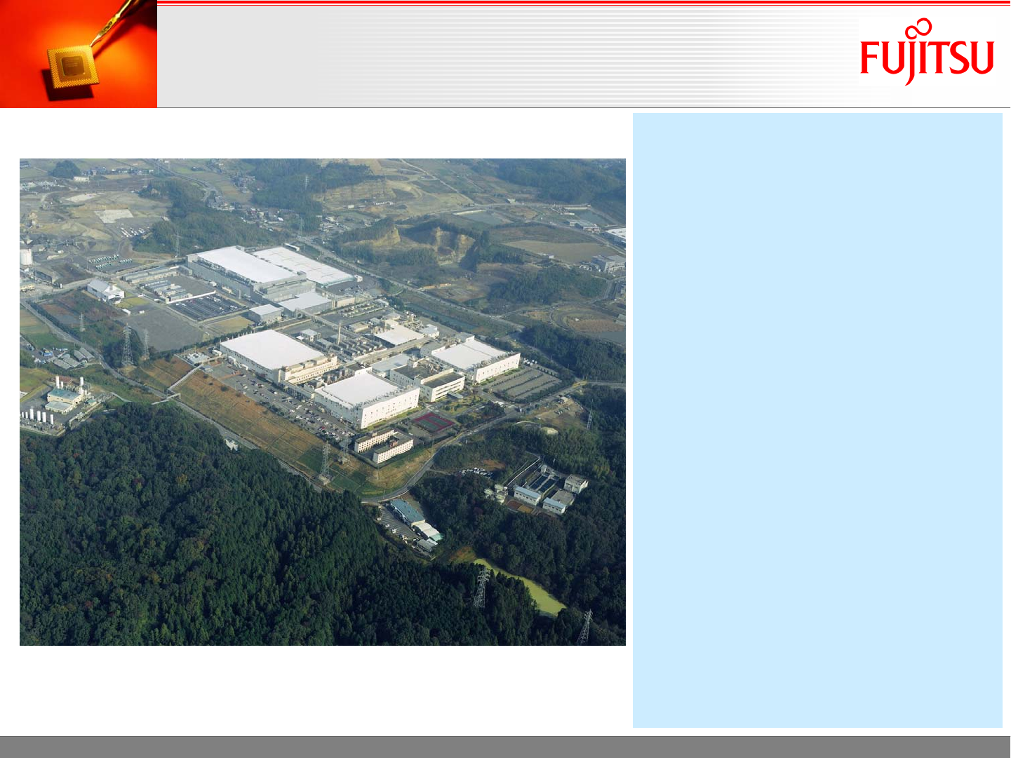
Fujitsu 65nm New 300mm Fabs – Mie, Japan
300mm Fab No.2
•Process
•65nm/90nm CMOS Logic
•Structural Features
•Seismic-vibration control
construction
•Clean room area: 24,000 sq. meters
•Production Capacity
•10,000 wafers per month (FY07
projection)
•Maximum capacity of 25,000 wafers
per month
•Planned Start of Operation
•April 2007
300mm Fab No.1
•Process
•90nm/65nm CMOS Logic
•Structural Features
•Seismic-control construction
•Clean room area: 12,000 sq. meters
•Production Capacity
•15,000 wafers per month (FY06)
•Start of Operation
•April 2005
3
February 7, 2006 DesignCon 2006
Leading-edge Technology
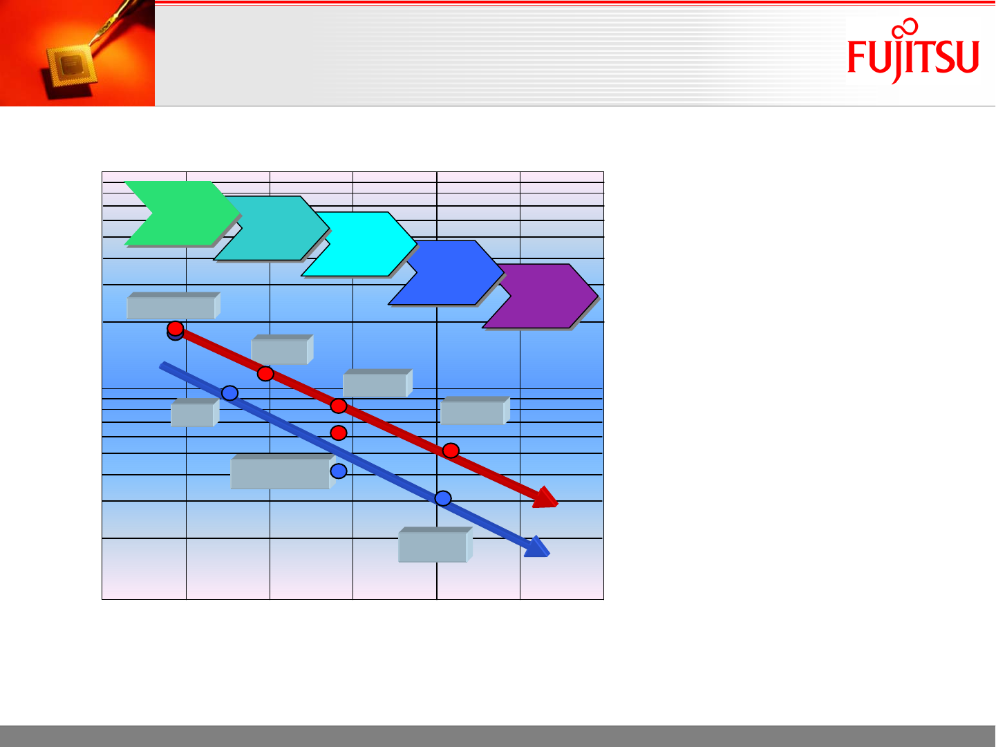
Fujitsu 65nm
1000
100
10
500
50
20
200
1998 2000 2002 2004 2006 2008 2010
Year (Production Start)
Physical Gate Length (nm)
45nm
45nm
65nm
65nm
90nm
90nm
130nm
130nm
180nm
180nm
CS100A
CS200
CS100HP
CS80 / 80A
CS90A
CS200A
CS90
CMOS Technology Roadmap
CS100/CS100A (90nm)
L actual=40-80nm
SiOC (k:2.9) low-k
Dual Damascene Cu
CS200/CS200A (65nm)
L actual=30-50nm
NCS (Nano
Nano-
-Clustering
Clustering
Silica)
Silica)
4
February 7, 2006 DesignCon 2006
Leading-edge Technology
Fujitsu 65nm Proven Track Record of 90nm
Complex Designs and Products
Proven Track Record of 90nm
Complex Designs and Products
5
February 7, 2006 DesignCon 2006
Leading-edge Technology
Fujitsu 65nm
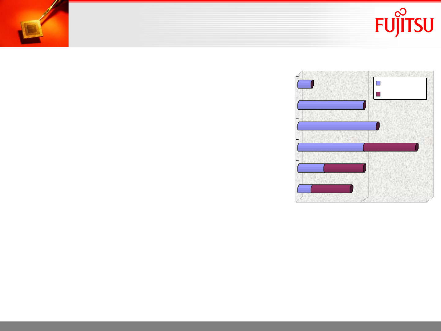
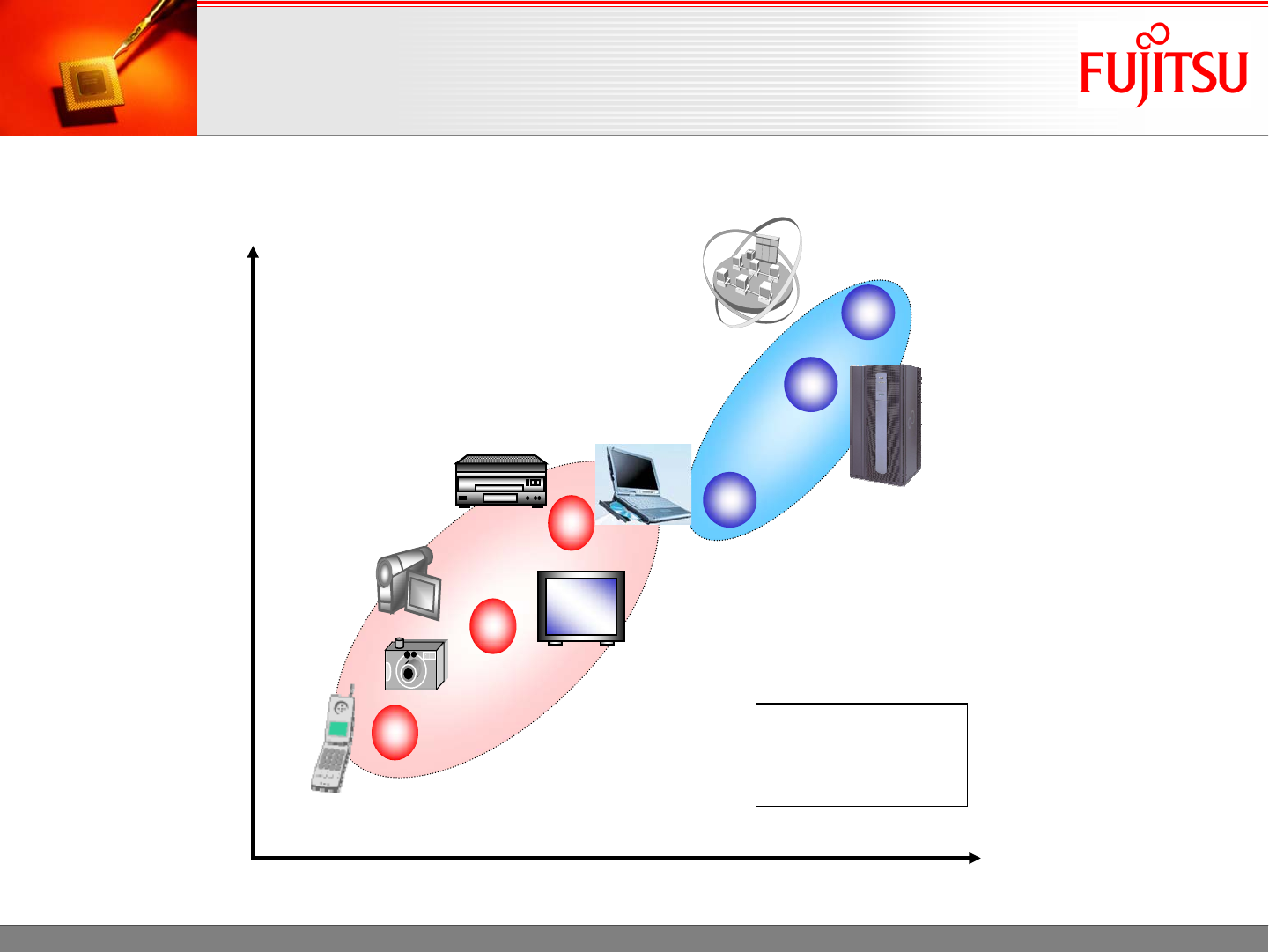
High-performance Products
PC CPU (Transmeta)
Large-scale FPGA (Lattice)
Others
Low-power Products
Multimedia processor
Digital AV products
Others
0510
Tape Out Number
20-50
50-100
100-200
200-250
250-350
350-450
Chip Size (mm2)
High End
Low Power
Proven Track Record of 90nm
Complex Designs and Products – continued
Proven Track Record of 90nm
Complex Designs and Products – continued

6
February 7, 2006 DesignCon 2006
Leading-edge Technology
Fujitsu 65nm 65nm, CS200 / 200A Features
65nm, CS200 / 200A Features
Features
Ultra-high-speed performance (CS200)
LG= 30nm, on-current enhance
Compared to 90nm technology, CS200 offers:
1.3 times faster speed
0.6 times lower power
2 times higher density
3 variations of Vth on a chip (CS200A)
(1.8V & 2.5V) or (1.8V & 3.3V) I/O combination available
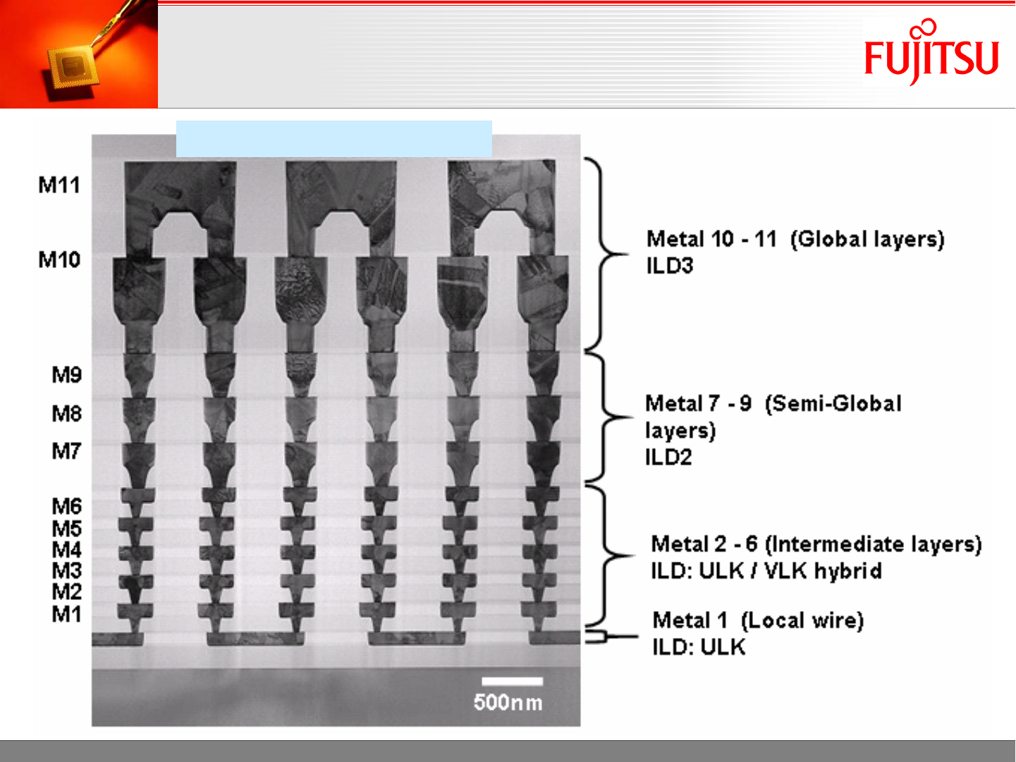
11-layer copper interconnects with robust, very low K ILD
7
February 7, 2006 DesignCon 2006
Leading-edge Technology
Fujitsu 65nm CS200 / 200A Transistor Variations
CS200: Ultra High Speed
CS200A: Wide Speed Range + Low Power Consumption
Speed
Leakage current
Fast
Large
High End
Server
STD-Tr
LL-Tr
Server/
Network
Digital
Consumer
Cellular Phone
STD-Tr
HS-Tr
HVt-Tr
Mobile
Computing
HS:High speed
STD:Standard
LL:Low leakage
HS-Tr
CS200
CS200A
8
February 7, 2006 DesignCon 2006
Leading-edge Technology
Fujitsu 65nm
Performance
Large
Small
SlowFast
tpd ×P
65nm
node
90nm
node
45nm
node
Leading-edge Transistors
Propagation Delay
Leakage
9
February 7, 2006 DesignCon 2006
Leading-edge Technology
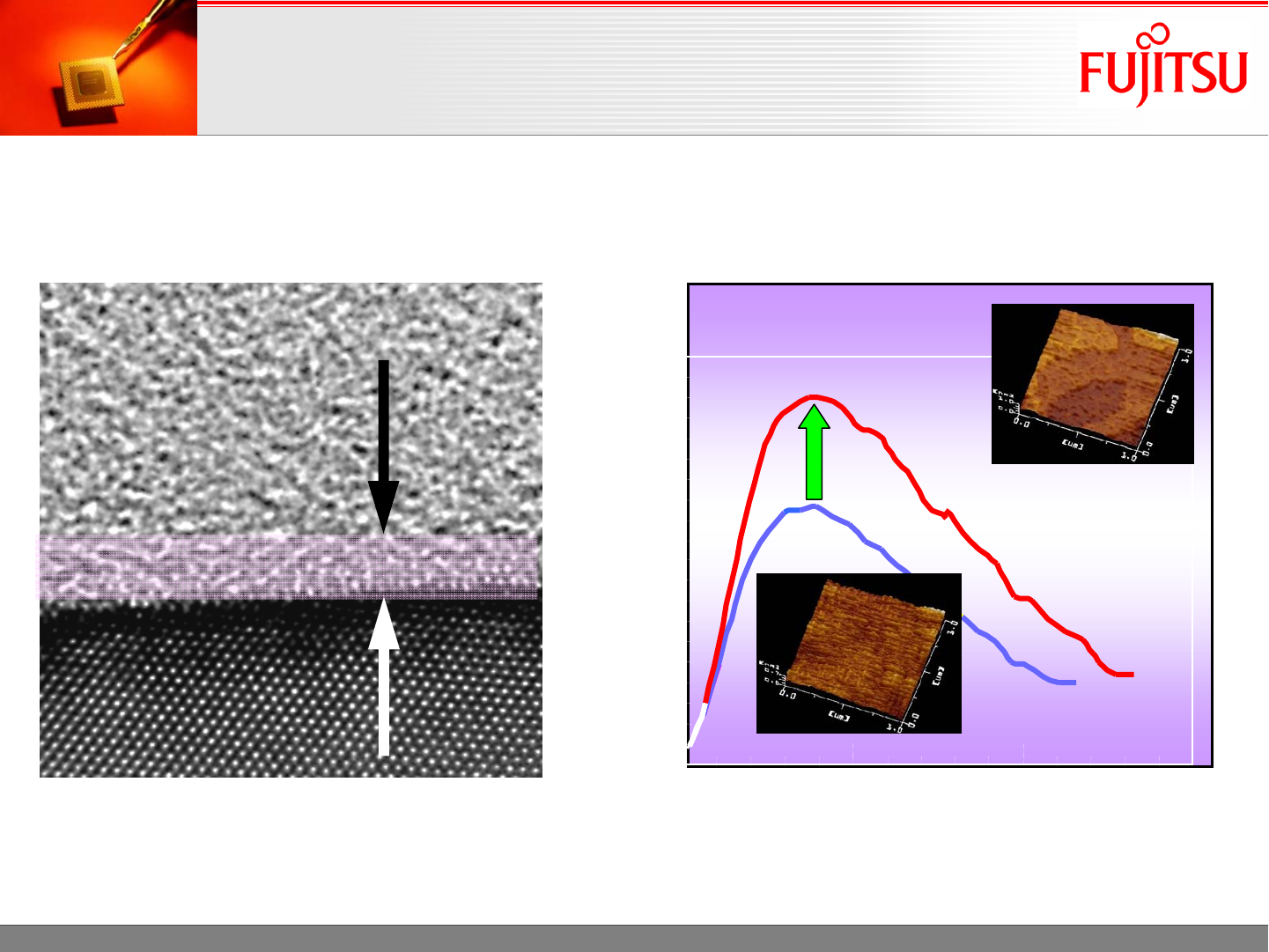
Fujitsu 65nm
1nm-thick Gate Oxide Surface Cleaning
Ultra-Thin Gate Insulator /
Mobility Improvement
Electric Field [MV/cm]
Normalized gm(∝mobility)
0.0
5.0E-4
1.0E-3
1.5E-3
2.0E-3
-0.5 1.5 3.5 5.5
After
optimize
Before
40% increase
Si substrate
Nitrided-SiO2
Poly-Si

10
February 7, 2006 DesignCon 2006
Leading-edge Technology
Fujitsu 65nm Speed Performance Improvements
Speed Performance Improvements
65nm 90nm
CS200 CS100 Delay
(ps/gate) (ps/gate) Improvement
Inverter 5.7 7.0 19%
2-input NAND 8.7 11.4 24%
2-input NAND + 200 grid interconnect load 23.1 30.8 25%
11
February 7, 2006 DesignCon 2006
Leading-edge Technology
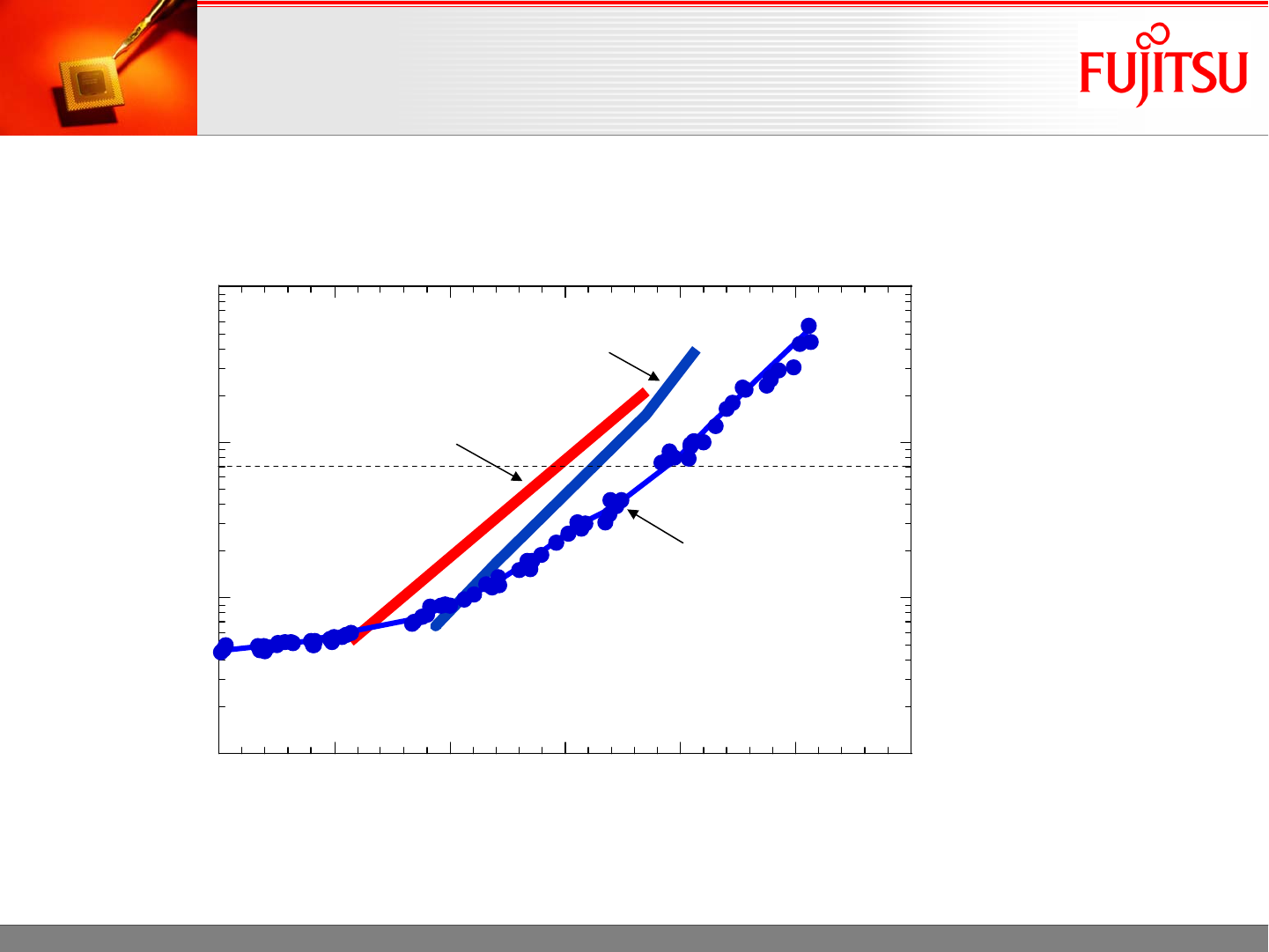
Fujitsu 65nm High-Performance Competitive Transistors
Ion vs Ioff Characteristics of nMOSFETs
Company 2)
A
Fujitsu
70nA/μm
10-9
10-8
10-7
10-6
0.7 0.8 0.9 1.0 1.1 1.2 1.3
Ioff (A/um)
Ion (uA/um)
Vd=1.0V
Company 1)
B
Ref.
1, 2) 2004 Symposium
on VLSI Technology
12
February 7, 2006 DesignCon 2006
Leading-edge Technology
Fujitsu 65nm Advanced Cu and Low-k
180nm node 130nm node 90nm node
CS80/80A
6-Cu layers
ILD FSG CS90A
7-Cu layers
ILD hybrid low-k CS100/100A/150
10-Cu layers
ILD full low-k
65nm node
Dielectric constant
High
Low
CS200/200A/250
11-Cu layers
ILD hybrid
Ultra-low K
ILD: Inter-layer Dielectric
Four Generations of Experience
13
February 7, 2006 DesignCon 2006
Leading-edge Technology
Fujitsu 65nm Fujitsu
Fujitsu’
’s Low
s Low-
-k Leads ITRS
k Leads ITRS
CS90
SiLKTM
/SiO 2
CS100
Full- SiOC CS200
NCS/ SiOC CS300
Full - NCS
K=2.7/4.1 K=2.9/2.9 K=2.25/2.9 K=2.25/2.25
k
Width [nm]
0
500
400
300
200
100
2000 2005 2010 2015
3.0
2.5
2.0
1.5
1.0
Products Year
CMOS Technology Node
CMOS Technology Node
Intermediate
Intermediate
Wire Pitch
Wire Pitch
130nm
130nm 90nm
90nm 65nm
65nm 45nm
45nm 32nm
32nm
k
<1.9
<2.4
<2.1
<2.7
14
February 7, 2006 DesignCon 2006
Leading-edge Technology
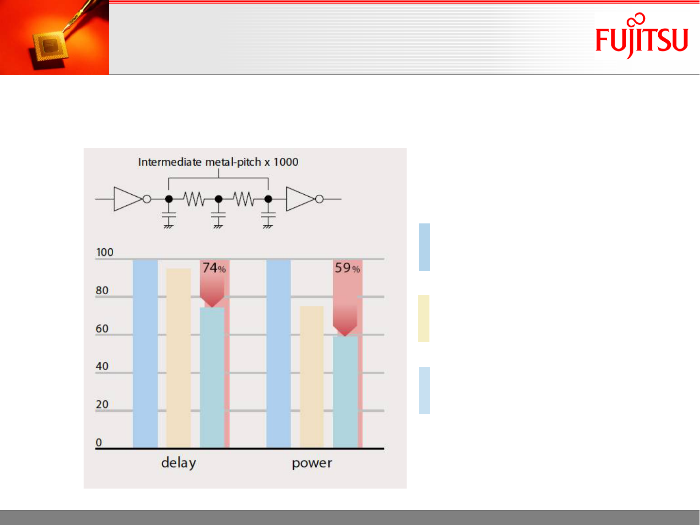
Fujitsu 65nm Low-k Advantages of 65nm
Ultra low-k impacts on speed and power dissipation
CS100A (90nm)
with SiOC/SiOC
Rsh: 90mΩ/sq., C: 56fF/1000 grid
CS200A (65nm)
with SiOC/SiOC
Rsh: 150mΩ/sq., C: 52fF/1000 grid
CS200A (65nm)
with NCS/SiOC
Rsh: 150mΩ/sq., C: 40fF/1000 grid
15
February 7, 2006 DesignCon 2006
Leading-edge Technology
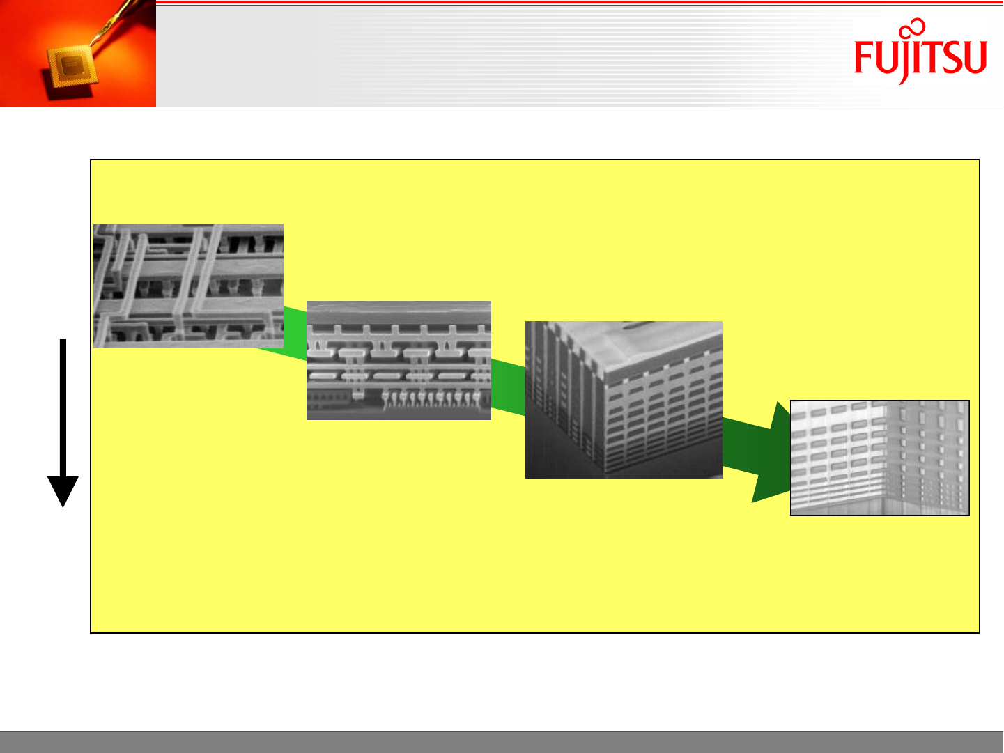
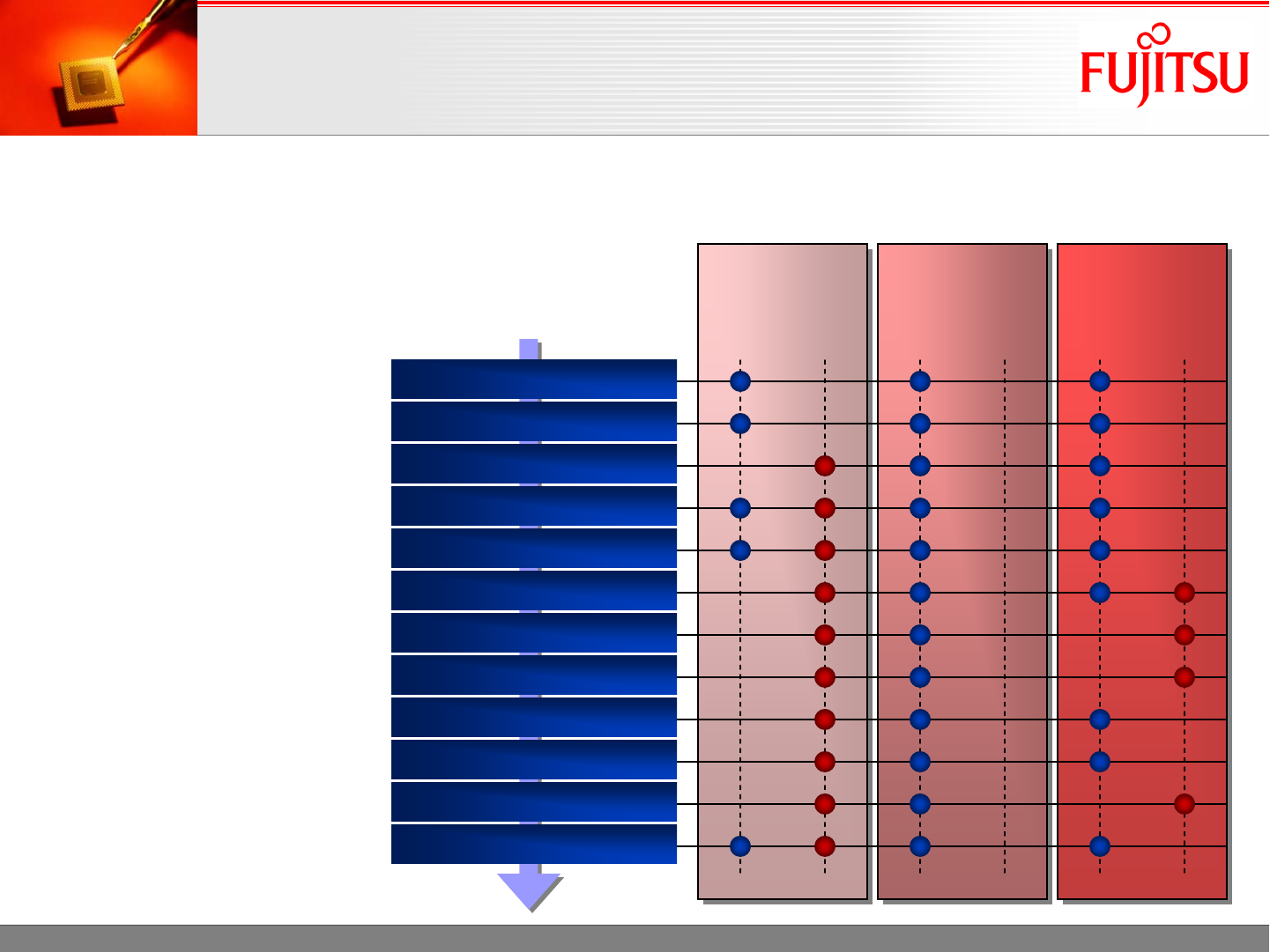
Fujitsu 65nm 11-Layer Copper Interconnects
Cu 11-layer Stack-via Chain
16
February 7, 2006 DesignCon 2006
Leading-edge Technology
Fujitsu 65nm The Fujitsu Ecosystem
The Fujitsu Ecosystem
Packaging,
Assembly
& Test
Packaging,
Packaging,
Assembly
Assembly
& Test
& Test
Process
Technology
Process
Process
Technology
Technology
Library
Development
Library
Library
Development
Development
IP
Development
& Support
IP
IP
Development
Development
& Support
& Support
Application
& Software
Support
Application
Application
& Software
& Software
Support
Support
Design
Methodology
Design
Design
Methodology
Methodology
Design
Services
Design
Design
Services
Services
EDA
Vendors 3rd Party
Design
Houses
3rd Party
IP Vendors
3rd Party
Library
Vendors
3rd Party
Test
Houses
17
February 7, 2006 DesignCon 2006
Leading-edge Technology
Fujitsu 65nm Fujitsu Technology Access
Fujitsu Technology Access
ASIC
Flow
Customer Fujitsu
COT
Flow
Customer Fujitsu
Custom
Flow
Customer Fujitsu
Clock Tree Synthesis
Clock Tree Synthesis
RTL Design
RTL Design
Physical Synthesis
Physical Synthesis
Logical Synthesis
Logical Synthesis
DFT Insertion
DFT Insertion
Formal Verification
Formal Verification
Floorplanning
Floorplanning
Routing
Routing
Test Validation
Test Validation
Physical Verification
Physical Verification
STA / ECO
STA / ECO
Timing & SI Verification
Timing & SI Verification
Flexible collaboration models
provide easy access to Fujitsu’s
leading-edge process for the
development of highly complex
silicon products
18
February 7, 2006 DesignCon 2006
Leading-edge Technology
Fujitsu 65nm Design Flow & Methodology
Design Flow & Methodology
Reference design flow - Fujitsu’s leading-edge design methodology
focuses on timing, signal and power integrity closure
Support for both Cadence SOCEncounterTM and Synopsys GalaxyTM
platforms
In-house CAD software development augments leading third-party EDA
solutions
Ensures silicon correlation and a fast path to silicon success by
combining Fujitsu’s strengths in process, CAD tool and methodology
development with design experience and expertise
Production proven flows used on 100+ multi-million-gate designs at 180,
130 and 90nm
Constantly updated and improved to address all issues at each process
node

19
February 7, 2006 DesignCon 2006
Leading-edge Technology
Fujitsu 65nm Fujitsu Design Services
Fujitsu Design Services
Library and tool support
Methodology development and support
High-speed I/O design and expertise
Vertical expertise and IP cores
RTL design
Synthesis and physical synthesis
Design partitioning and floorplanning
Static timing analysis
Test insertion and ATPG generation
Place and route
Timing and SI closure
Formal verification
Physical verification
Test and product engineering
20
February 7, 2006 DesignCon 2006
Leading-edge Technology
Fujitsu 65nm
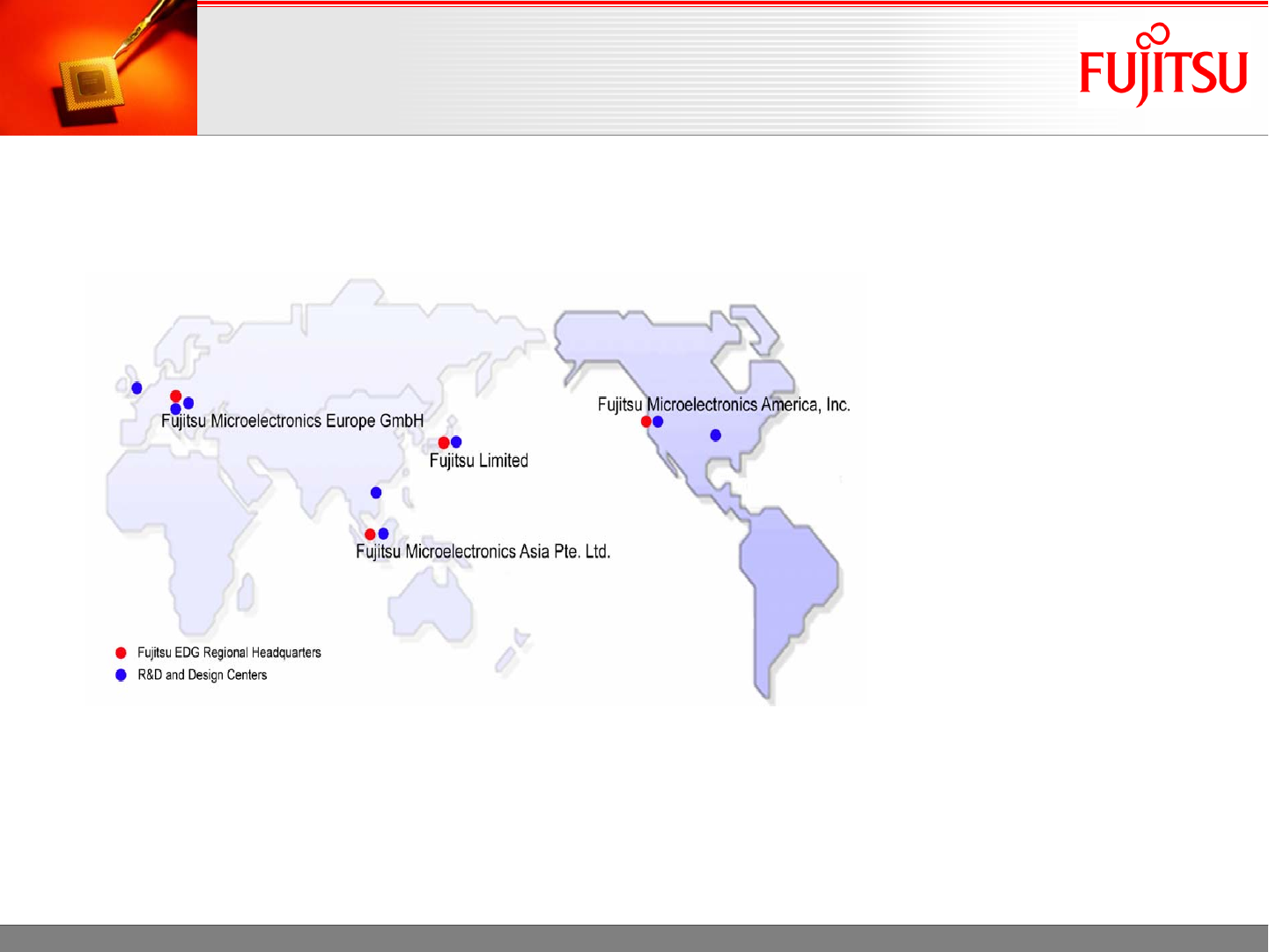
Global Presence
Local design centers around the world provide design
services for all phases of the development process
Skilled engineering teams experienced in development of large complex
designs at 130nm and below
100+ multi-million gate designs taped out
Fujitsu Worldwide Design Centers
Fujitsu Worldwide Design Centers

21
February 7, 2006 DesignCon 2006
Leading-edge Technology
Fujitsu 65nm Summary
Summary
Fujitsu Objective
Helping customers accelerate their innovation, differentiate their
products and enhance their competitive advantage, therefore
helping them succeed
Leading-edge technologies
Strength in process technologies
90nm, 65nm and beyond
Partnerships and customer collaborations
Flexible customer engagements and close collaborations
Early customer engagements
Tailored support and services to meet customer needs
System-level LSI solutions
ASIC and ASSP/SoC, including10GbE switch chip and
WiMAX SoC
Full design and development environments and support