Fujitsu AD81 00001 14E IC Package A810000114e
User Manual: Fujitsu IC Package Packaging ation - Fujitsu United States
Open the PDF directly: View PDF ![]() .
.
Page Count: 10
2011.1
FUJITSU SEMICONDUCTOR
IC
Package
se
es
ng
se
ny
ht
or
ut
ed
ct
in
in
es
es
of
ns
IC-package_E.fm 1 ページ 2011年1月27日 木曜日 午後5時44分
2011.1
FUJITSU S
For further information please contact:
North and South America
FUJITSU SEMICONDUCTOR AMERICA, INC.
1250 E. Arques Avenue, M/S 333
Sunnyvale, CA 94085-5401, U.S.A.
Tel: +1-408-737-5600 Fax: +1-408-737-5999
http://us.fujitsu.com/micro/
Europe
FUJITSU SEMICONDUCTOR EUROPE GmbH
Pittlerstrasse 47, 63225 Langen, Germany
Tel: +49-6103-690-0 Fax: +49-6103-690-122
http://emea.fujitsu.com/semiconductor/
Korea
FUJITSU SEMICONDUCTOR KOREA LTD.
206 Kosmo Tower Building, 1002 Daechi-Dong,
Gangnam-Gu, Seoul 135-280, Republic of Korea
Tel: +82-2-3484-7100 Fax: +82-2-3484-7111
http://kr.fujitsu.com/fmk/
Asia Pacific
FUJITSU SEMICONDUCTOR ASIA PTE. LTD.
151 Lorong Chuan,
#05-08 New Tech Park 556741 Singapore
Tel : +65-6281-0770 Fax : +65-6281-0220
http://www.fujitsu.com/sg/services/micro/semiconductor/
FUJITSU SEMICONDUCTOR SHANGHAI CO., LTD.
Rm. 3102, Bund Center, No.222 Yan An Road (E),
Shanghai 200002, China
Tel : +86-21-6146-3688 Fax : +86-21-6335-1605
http://cn.fujitsu.com/fss/
FUJITSU SEMICONDUCTOR PACIFIC ASIA LTD.
10/F., World Commerce Centre, 11 Canton Road,
Tsimshatsui, Kowloon, Hong Kong
Tel : +852-2377-0226 Fax : +852-2376-3269
http://cn.fujitsu.com/fsp/
Specifications are subject to change without notice. For further information please contact each office.
All Rights Reserved.
The contents of this document are subject to change without notice.
Customers are advised to consult with sales representatives before ordering.
The information, such as descriptions of function and application circuit examples, in this document are presented solely for the purpose
of reference to show examples of operations and uses of FUJITSU SEMICONDUCTOR device; FUJITSU SEMICONDUCTOR does
not warrant proper operation of the device with respect to use based on such information. When you develop equipment incorporating
the device based on such information, you must assume any responsibility arising out of such use of the information.
FUJITSU SEMICONDUCTOR assumes no liability for any damages whatsoever arising out of the use of the information.
Any information in this document, including descriptions of function and schematic diagrams, shall not be construed as license of the use
or exercise of any intellectual property right, such as patent right or copyright, or any other right of FUJITSU SEMICONDUCTOR or any
third party or does FUJITSU SEMICONDUCTOR warrant non-infringement of any third-party's intellectual property right or other right
by using such information. FUJITSU SEMICONDUCTOR assumes no liability for any infringement of the intellectual property rights or
other rights of third parties which would result from the use of information contained herein.
The products described in this document are designed, developed and manufactured as contemplated for general use, including without
limitation, ordinary industrial use, general office use, personal use, and household use, but are not designed, developed and manufactured
as contemplated (1) for use accompanying fatal risks or dangers that, unless extremely high safety is secured, could have a serious effect
to the public, and could lead directly to death, personal injury, severe physical damage or other loss (i.e., nuclear reaction control in
nuclear facility, aircraft flight control, air traffic control, mass transport control, medical life support system, missile launch control in
weapon system), or (2) for use requiring extremely high reliability (i.e., submersible repeater and artificial satellite).
Please note that FUJITSU SEMICONDUCTOR will not be liable against you and/or any third party for any claims or damages
arising in connection with above-mentioned uses of the products.
Any semiconductor devices have an inherent chance of failure. You must protect against injury, damage or loss from such failures
by incorporating safety design measures into your facility and equipment such as redundancy, fire protection, and prevention of
overcurrent levels and other abnormal operating conditions.
Exportation/release of any products described in this document may require necessary procedures in accordance with the regulations
of the Foreign Exchange and Foreign Trade Control Law of Japan and/or US export control laws.
The company names and brand names herein are the trademarks or registered trademarks of their respective owners.
FUJITSU SEMICONDUCTOR LIMITED
Nomura Fudosan Shin-yokohama Bldg. 10-23, Shin-yokohama 2-Chome,
Kohoku-ku Yokohama Kanagawa 222-0033, Japan
Tel: +81-45-415-5858
http://jp.fujitsu.com/fsl/en/
© 2002-2011 FUJITSU SEMICONDUCTOR LIMITED Printed in Japan
AD81-00001-14E January, 2011
Edited: Sales Promotion Department
IC-package_E.fm 20 ページ 2011年1月27日 木曜日 午後5時44分
Q
System in P
Providing New Technologies for the NearProviding New Technologies for the Near
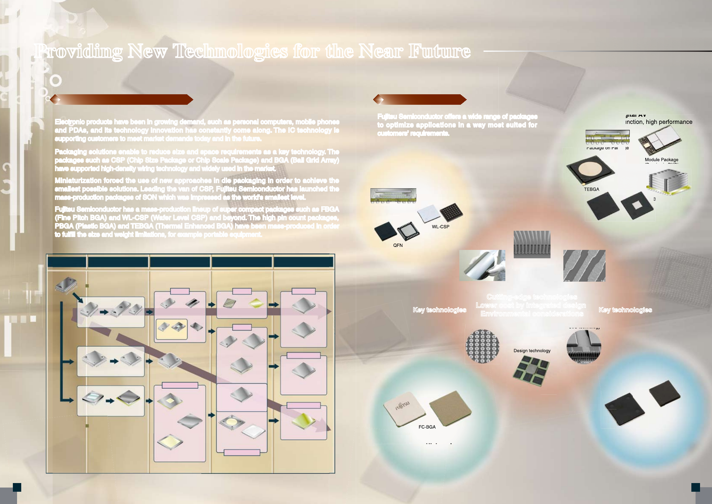
Electronic products have been in growing demand, such as personal computers, mobile phones
and PDAs, and its technology innovation has constantly come along. The IC technology is
supporting customers to meet market demands today and in the future.
Packaging solutions enable to reduce size and space requirements as a key technology. The
packages such as CSP (Chip Size Package or Chip Scale Package) and BGA (Ball Grid Array)
have supported high-density wiring technology and widely used in the market.
Miniaturization forced the use of new approaches in die packaging in order to achieve the
smallest possible solutions. Leading the van of CSP, Fujitsu Semiconductor has launched the
mass-production packages of SON which was impressed as the world's smallest level.
Fujitsu Semiconductor has a mass-production lineup of super compact packages such as FBGA
(Fine Pitch BGA) and WL-CSP (Wafer Level CSP) and beyond. The high pin count packages,
PBGA (Plastic BGA) and TEBGA (Thermal Enhanced BGA) have been mass-produced in order
to fulfill the size and weight limitations, for example portable equipment.
Trends in Package Development Pa
Fujitsu
to opt
custom
Fujitsu
to opt
custom
- Supe
- Ultra hig
1980s 1990s 2000s 2010s
Miniaturization
DIP
FBGA
BCC
FD-FBGA
CSP
WL-CSP Bare Die
KGD Module
EWLP
Embedded Die
SOJ TSOP SSOP
CSOP SON
LQFP
SiP
Stacked-FBGA
PoP
3D Package
3D CHIP Stacked
(TSV Technology)
QFP SQFP
High Performance
FDH-BGA
TAB-BGA
EBGA
TEBGA
FC-BGA
High-speed
COC
High-speed
H-SiP
PGA BGA
Enhanced BGA
2
IC-package_E.fm 2 ページ 2011年1月27日 木曜日 午後5時44分
WL-CSP
QFN
Ultra thin technology
Fine-pitch technology
Fine wiring
Bump technology
Design technology
CoC technology
QFP
BGA/FBGA
FC-BGA
System in Package
Module Package
(Passive in PKG)
Package on Package
TEBGA
3D-Chip stack
Key technologiesKey technologies Key technologiesKey technologies
Cutting-edge technologies
Lower cost by integrated design
Environmental considerations
Cutting-edge technologies
Lower cost by integrated design
Environmental considerations
TEQFP
r the Near Futurer the Near Future
phones
ology is
ogy. The
d Array)
eve the
hed the
s FBGA
ckages,
in order
phones
ology is
ogy. The
d Array)
eve the
hed the
s FBGA
ckages,
in order
Package Solutions
Fujitsu Semiconductor offers a wide range of packages
to optimize applications in a way most suited for
customers' requirements.
Fujitsu Semiconductor offers a wide range of packages
to optimize applications in a way most suited for
customers' requirements.
Digital AV
- High density, high function, high performance -
Mobile
- Super compact, light, thin -
High-end
- Ultra high speed, high efficiency heat dissipation -
Automotive
- High reliability, high heat resistance -
e
e
ked
gy)
3
IC-package_E.fm 3 ページ 2011年1月27日 木曜日 午後5時44分
4
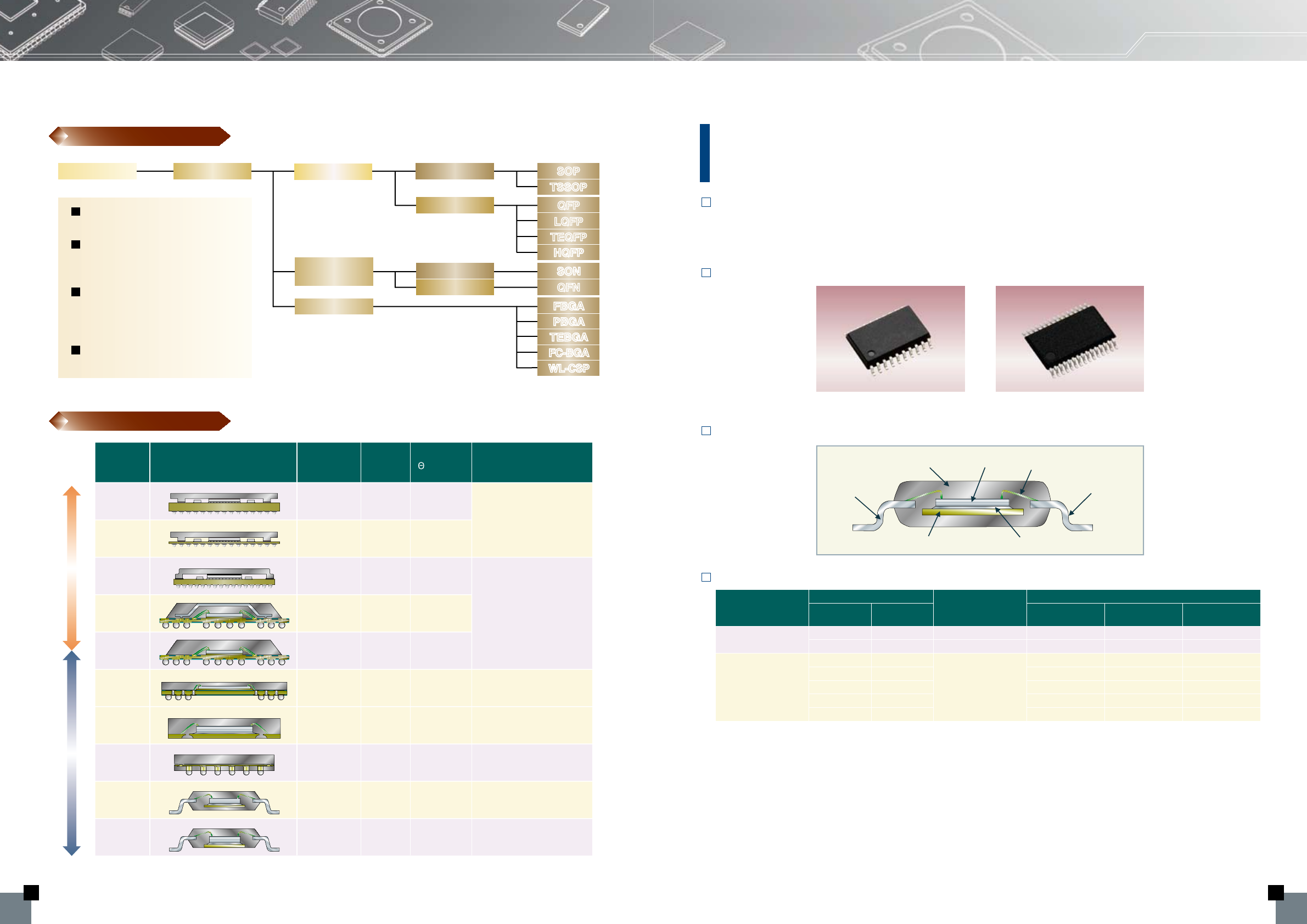
Package structure
Package
type Pin count
FC-CBGA 450~2116 ~5 7~
Routers, Servers,
Workstations,
Backbone transmission devices
Routers,
Personal computers,
Graphics, Digital TVs,
Set top boxes,
Printers
Application
I/O
frequency
(GHz)
7~~2.5450~2116
FC-PBGA
(AlSiC-LID)
9~~2.5450~1156
FC-PBGA
(Cu-LID)
13~
~1.6256~1156TEBGA
15~~1.6256~1156PBGA
Personal computers,
Mobile phones,
Digital video cameras,
Digital still cameras, PDAs
17~60~166~906FBGA
High-end
Consumer
appliances
Mobile phones,
Digital video cameras,
Digital still cameras, PDAs
20~40~1.56~68
SON
QFN
Mobile phones,
Digital video cameras,
Digital still cameras, PDAs
25~60~2.542~309WL-CSP
Personal computers,
Digital TV, Set top boxes,
Printers
15~100~2.548~304
QFP
LQFP
Personal computers,
Digital TV, Set top boxes
15~35~2.548~256
TEQFP
Package Surface mount
Flat type Dual lead
Quad lead
SOP
SOP
TSSOP
TSSOPTSSOPTSSOP
Matrix type
QFP
QFP
Quad lead QFN
QFN
TEQFP
TEQFPTEQFP
HQFP
HQFPHQFPHQFPHQFP
FBGA
FBGAFBGAFBGAFBGA
Leadless chip
carrier SON
SONSONSONSON
PBGA
PBGAPBGAPBGAPBGA
TEBGA
TEBGATEBGATEBGATEBGA
FC-BGAFC-BGAFC-BGAFC-BGAFC-BGA
WL-CSP
WL-CSPWL-CSPWL-CSPWL-CSP
Dual lead
LQFP
LQFP
Package Line-up
Multi-pin
QFP,PBGA,TEBGA,FC-BGA
Thin and compact
TSSOP,LQFP,TEQFP,SON,QFN,
FBGA,WL-CSP
High efficiency heat dissipation and
large chip support
HQFP,TEQFP,PBGA,TEBGA,
FC-BGA
High speed
FC-BGA
Package Overview
Heat
resistance
ja(ºC /W)
(0m/s)
IC-package_E.fm 4 ページ 2011年1月27日 木曜日 午後5時44分
IC Package
IC Package
5
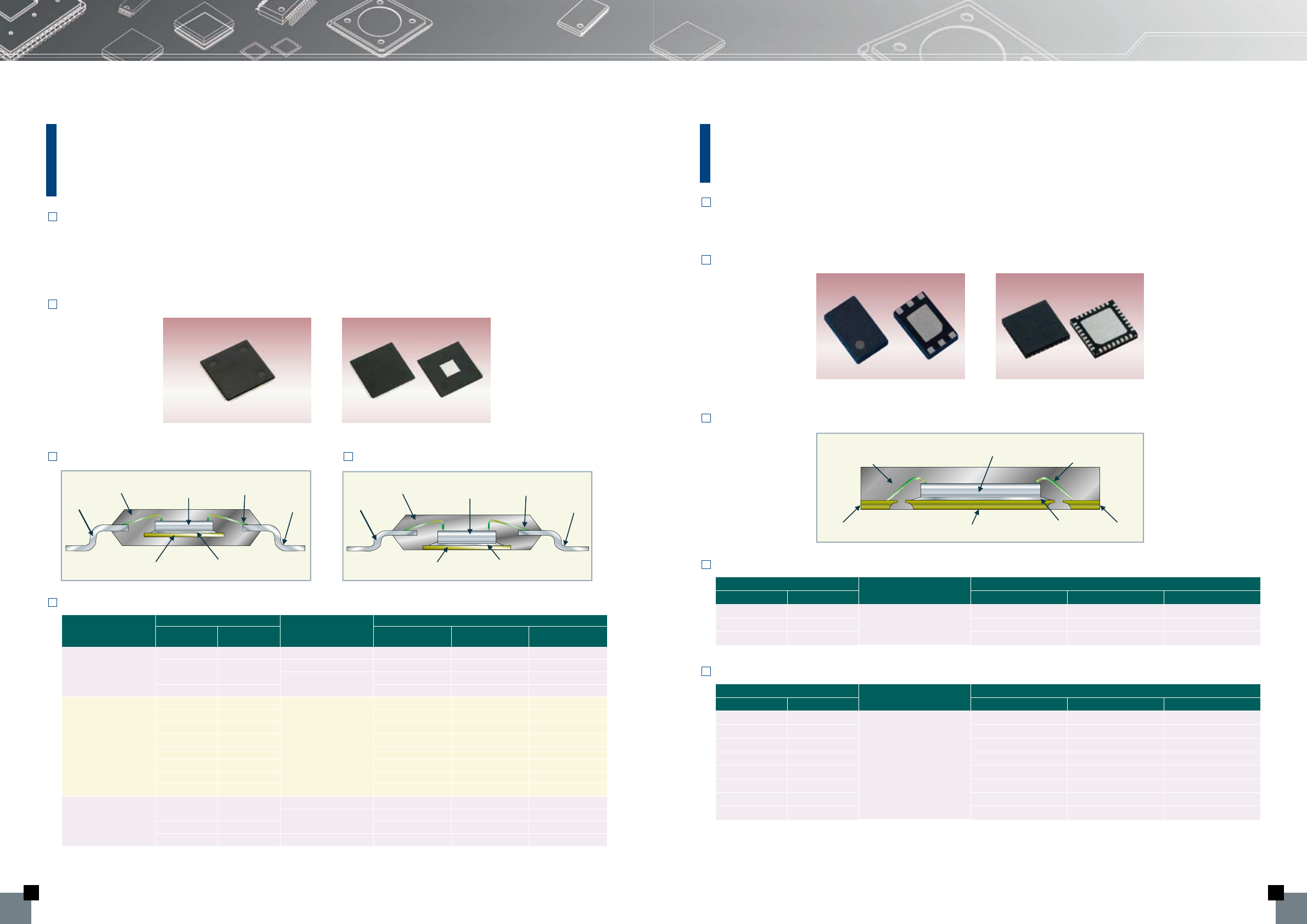
SOP (Small Outline L-Leaded Package)
TSSOP(Thin Shrink Small Outline Package)
■ Features
● Superior cost performance with a mature technology.
● High reliability in mounting the package on printed circuit boards.
● Thin and compact.
■ SOP and TSSOP Package external view
■ SOP and TSSOP Package cross section
■ SOP and TSSOP Package line-up
Please contact us for information on other packages.
SOP TSSOP
Package type
Package size (mm)
Mounting height (mm)
Pin count
XY Pin pitch
1.27mm
Pin pitch
0.65mm
Pin pitch
0.50mm
SOP 5.3 5.24 2.10 Max. 8- -
7.5 12.7 2.65 Max. 20 - -
TSSOP
4.4 3.1
1.20 Max.
-8-
4.4 4.96 -14/16 -
4.4 6.5 -20 24
4.4 7.8 -24 30
4.4 9.7 -28 -
Lead
Wire
LSI Chip
Mold Resin
Stage Adhesive
Solder Plating
IC-package_E.fm 5 ページ 2011年1月27日 木曜日 午後5時44分
6
QFP (Quad Flat Package)
LQFP (Low Profile Quad Flat Package)
TEQFP (Thermally Enhanced QFP)
HQFP (QFP with Heat Sink)
■ Features
● Equipped with outer leads at the four corners of the package.
● Superior cost performance with a mature technology.
● High reliability in mounting the package on printed circuit boards.
● TEQFP and HQFP can be mounted with a chip with high heat emission because of their high efficiency in
heat dissipation.
■ QFP Package external view
■ QFP and LQFP Package cross section ■ TEQFP Package cross section
■ QFP Packages line-up
Please contact us for information on other packages.
LQFP TEQFP
Lead
Wire
LSI Chip
Mold Resin
Stage Adhesive
Solder Plating
Lead
Wire
LSI Chip
Mold Resin
Stage Adhesive
Solder Plating
Package type
Package size (mm)
Mounting height (mm)
Pin count
X Y Pin pitch
0.65mm
Pin pitch
0.50mm
Pin pitch
0.40mm
QFP
14.0 20.0 3.35 Max. 100 - -
28.0 28.0 3.95 Max. -208 -
4.03 Max. - - 256
32.0 32.0 -240 -
LQFP
TEQFP
7.0 7.0
1.70 Max.
-48 64
10.0 10.0 52 64 -
12.0 12.0 64 80 -
14.0 14.0 -100 -
16.0 16.0 -120 144
20.0 20.0 -144 -
24.0 24.0 -176 216
28.0 28.0 -208 256
HQFP
28.0 28.0 3.95 Max. -208 -
4.03 Max. - - 256
32.0 32.0 -240 296
40.0 40.0 4.10 Max. -304 -
IC-package_E.fm 6 ページ 2011年1月27日 木曜日 午後5時44分
IC Package
IC Package
7
SON (Small Outline Non-leaded Package)
QFN (Quad Flat Non-Leaded Package)
■ Features
● Thin and compact.
● Better cost performance compared to BGA.
■ Package external view
■ Package cross section
■ SON Package line-up
■ QFN Package line-up
Please contact us for information on other packages.
SON QFN
Package size (mm)
Mounting height (mm) Pin count
XY Pin pitch 0.65mm Pin pitch 0.50mm Pin pitch 0.40mm
1.80 2.85
0.80 Max.
6- -
2.0 2.0 -8-
3.0 3.0 -10 -
Package size (mm)
Mounting height (mm) Pin count
XY Pin pitch 0.65mm Pin pitch 0.50mm Pin pitch 0.40mm
2.5 3.5
0.80 Max.
- - 24
3.0 3.0 -16 20
4.0 4.0 16 16/20/24 28
5.0 5.0 -28/32 40
6.0 6.0 -40 48
7.0 7.0 -48 56
8.0 8.0 - - 68
9.0 9.0 -64 -
LSI Chip
Mold Resin
Adhesive
Stage
Wire
No Plating No Plating
IC-package_E.fm 7 ページ 2011年1月27日 木曜日 午後5時44分
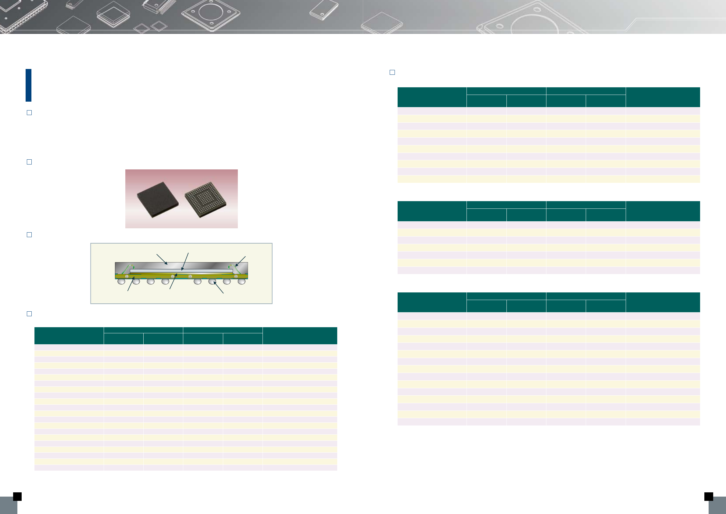
8
FBGA
(Fine pitch Ball Grid Array)
■ Features
Low profile and multi-pin support, suitable for portable devices such as mobile phones and DSCs.
● Fine pitch (pin pitch from 0.4mm) and thin.
● Superior electrical characteristics and reliability.
● Plentiful line-up and customization support.
■ FBGA Package external view
■ FBGA Package cross section
■ FBGA Package line-up
Pin pitch : 0.50mm (Less than 500pin)
*TB : Thermal Ball
Package code
Pin count Package size (mm)
Pin arrangement
Total number of TBs*
included X Y
BGA-66P-M01 66 95.0 5.0 2 rows
BGA-82P-M01 82 96.0 6.0 2 rows
BGA-96P-M04 96 06.0 6.0 3 rows
BGA-100P-M03 100 07.0 7.0 2 + (1) + 1 rows
BGA-112P-M05 112 07.0 7.0 3 rows (With nonexistent pins)
BGA-130P-M02 130 97.0 7.0 3 rows
BGA-144P-M09 144 07.0 7.0 4 rows
BGA-168P-M03 168 25 9.0 9.0 3 rows (With nonexistent pins)
BGA-208P-M01 208 09.0 9.0 4 rows
BGA-232P-M01 232 012.0 12.0 2 + (1) + 2 rows
BGA-240P-M02 289 49 10.0 10.0 4 rows
BGA-240P-M03 240 010.0 10.0 4 rows
BGA-289P-M01 289 25 10.0 10.0 3 + (1) + 2 rows
BGA-304P-M05 304 013.0 13.0 2 + (1) + 2 rows
BGA-304P-M07 304 012.0 12.0 4 rows
BGA-337P-M02 428 81 13.0 13.0 4 rows
BGA-345P-Mxx 345 25 12.0 12.0 2 + (1) + 2 + (1) + 1 rows
BGA-385P-M01 434 49 13.0 13.0 3 + (1) + 2 rows
BGA-385P-M02 385 81 13.0 13.0 2 + (2) + 2 rows
BGA-385P-M03 385 81 12.0 12.0 4 rows
BGA-400P-M04 481 81 15.0 15.0 4 rows
LSI Chip
Mold Resin
Adhesive
Solder Ball
Wire
PCB
IC-package_E.fm 8 ページ 2011年1月27日 木曜日 午後5時44分
IC Package
IC Package
9
■ FBGA Package line-up
Pin pitch : 0.50mm (500pin or more)
*TB : Thermal Ball
Pin pitch : 0.65mm
*TB : Thermal Ball
Pin pitch : 0.80mm
Please contact us for information on other pin arrangements. *TB : Thermal Ball
Package code
Pin count Package size (mm)
Pin arrangement
Total number of TBs*
included X Y
BGA-506P-Mxx 506 81 14.0 14.0 3 + (1) + 2 rows
BGA-562P-M03 562 81 14.0 14.0 3 + (1) + 3 rows
BGA-586P-Mxx 586 121 15.0 15.0 3 + (1) + 2 rows
BGA-586P-M04 586 49 15.0 15.0 4 + (1) + 2 rows
BGA-610P-M01 610 121 16.0 16.0 3 + (2) + 2 rows
BGA-650P-M03 650 169 15.0 15.0 5 rows
BGA-753P-Mxx 753 169 18.0 18.0 3 + (1) + 2 rows
BGA-770P-M01 770 121 16.0 16.0 4 + (1) + 3 rows
BGA-842P-Mxx 842 169 18.0 18.0 3 + (1) + 2 rows
BGA-906P-Mxx 906 169 18.0 18.0 3 + (1) + 2 + (1) + 2 rows
Package code
Pin count Package size (mm)
Pin arrangement
Total number of TBs*
included X Y
BGA-176P-M05 176 011.0 11.0 4 rows
BGA-204P-M01 204 011.0 11.0 3 + (1) + 2 rows
BGA-240P-M07 240 013.0 13.0 4 rows
BGA-252P-M01 252 013.0 13.0 5 rows (With nonexistent pins)
BGA-280P-M03 280 013.0 13.0 5 rows
BGA-360P-M05 441 81 16.0 16.0 5 rows
BGA-385P-M04 385 25 16.0 16.0 5 rows
Package code
Pin count Package size (mm)
Pin arrangement
Total number of TBs*
included X Y
BGA-112P-M04 112 010.0 10.0 4 rows
BGA-144P-M06 144 012.0 12.0 4 rows
BGA-144P-M07 144 012.0 12.0 4 rows (With nonexistent pins)
BGA-176P-M04 176 012.0 12.0 5 rows (With nonexistent pins)
BGA-188P-M01 188 015.0 15.0 4 rows (With nonexistent pins)
BGA-192P-M06 192 -12.0 12.0 Full Matrix (With nonexistent pins)
BGA-224P-M06 224 016.0 16.0 4 rows
BGA-224P-M08 260 36 16.0 16.0 4 rows
BGA-224P-M09 288 64 16.0 16.0 4 rows
BGA-240P-M06 240 015.0 15.0 5 rows
BGA-256P-M17 256 49 18.0 18.0 2 + (1) + 2 rows
BGA-272P-M06 321 49 18.0 18.0 4 rows
BGA-272P-M08 272 018.0 18.0 4 rows
BGA-320P-M05 369 49 18.0 18.0 5 rows
BGA-441P-M01 441 -18.0 18.0 Full Matrix
IC-package_E.fm 9 ページ 2011年1月27日 木曜日 午後5時44分
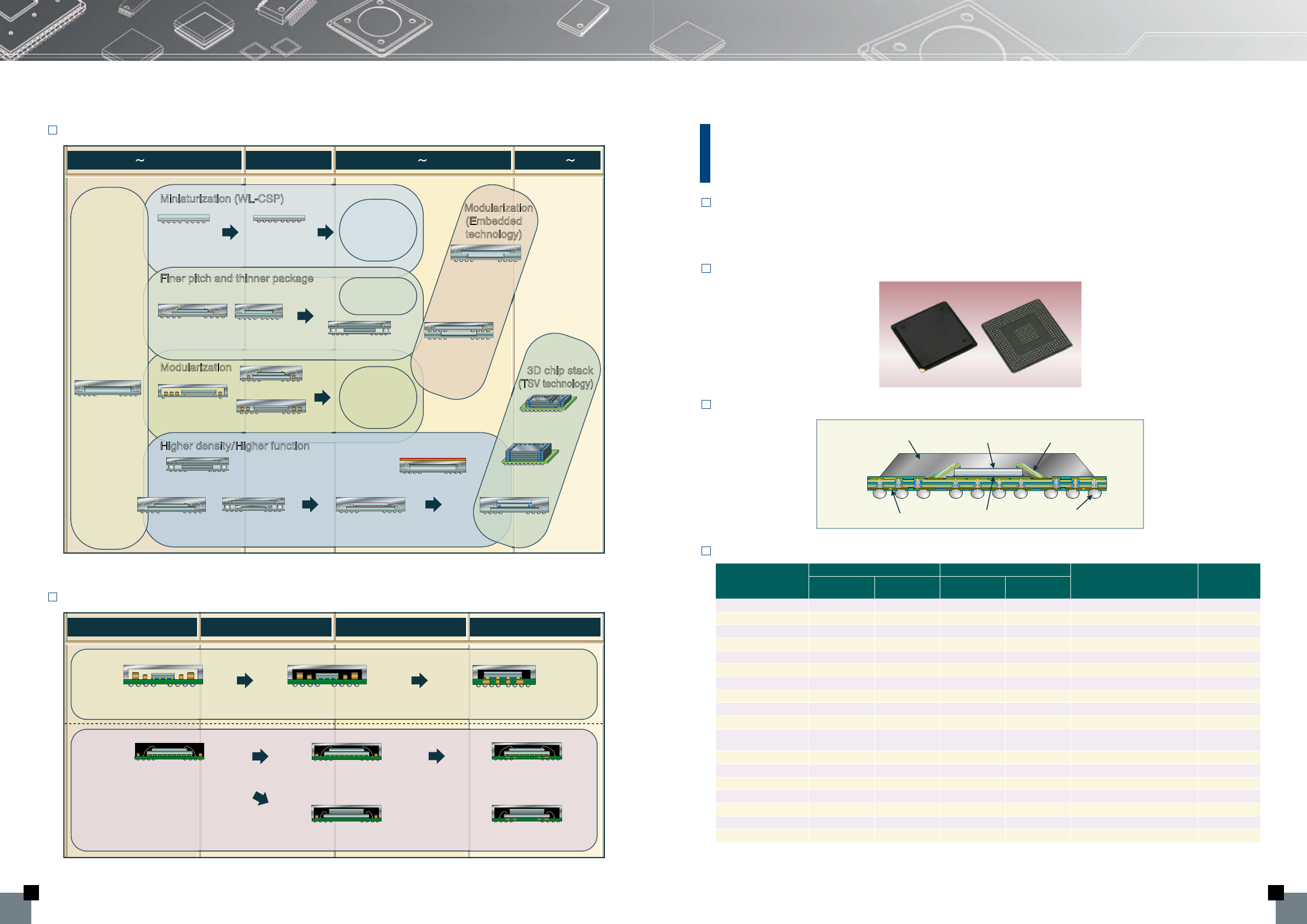
10
■ CSP Road map
Fujitsu Semiconductor will provide the most suitable SiP to the customer's requirements with our extensive implementation technologies.
Please contact us for any requests.
■ Module package road map
Package stack (PoP)
Package stack
(Thin PoP/FC)
Higher density/Higher function
Modularization
Finer pitch and thinner package
Miniaturization (WL-CSP)
Modularization
(Embedded
technology)
3D chip stack
(TSV technology)
Chip stack Package stack
(PoP/WB)
0.3mmt / 0.3mm
Pitch
Much thinner
package
and finer pitch
WL-CSP
Next development
in modules
Much thinner
package
0.35mmt / 0.4mm
Pitch
0.8mmt / 0.4mm
Pitch
3D Chip Stack
(Memory)
Chip on Chip
(TSV technology)
3D Chip Stack
(Logic/Memory)
FBGA
FBGA with low
thermal resistance
Chip on Chip
(Micro-bump)
On-chip passive
components (Wire)
On-chip passive
components mixture
(WLP) On-chip passive
components (FC)
Chip embedded
board PoP
(Passive/Active
components)
1.0mmt
Chip embedded
board
(Passive/Active
components)
2009 2010 2011 2013 2014
FCB
MCP
Passive components (L,C)
embedded
EMI measure (shield case)
Modularization Embedding in boardModularization
Modularization Modularization
COC+Modularization
Passive components (L,C)
embedded
Passive components (L,C)
embedded
EMI measure (Mold shield)
Passive components (L,C)
embedded
EMI measure (Mold shield)
Passive components (L,C)
embedded
EMI measure (Mold shield)
Passive components (L,C)
embedded in board
EMI measure (Mold shield)
Embedding in board
Passive components (L,C)
embedded in board
EMI measure (Mold shield)
COC+Embedding in board
Passive components (L,C)
embedded in board
EMI measure (Mold shield)
20112010 20122009
IC-package_E.fm 10 ページ 2011年1月27日 木曜日 午後5時44分
IC Package
IC Package
11
PBGA
(Plastic Ball Grid Array)
■ Features
● Sealed with plastic resin to achieve high cost performance.
● Superior support for multi-pin.
● Package sizes at 27mmSQ, 31mmSQ, and 35mmSQ are available.
■ PBGA Package external view
■ PBGA Package cross section
■ PBGA Package line-up
Please contact us for information on other pin arrangements. *TB : Thermal Ball
Package code
Pin count Package size (mm)
Pin arrangement Pin pitch
(mm)
Total number of
TBs* included X Y
BGA-256P-M24 256 -17.0 17.0 Full Matrix 1.00
BGA-256P-M27 256 027.0 27.0 4 rows 1.27
BGA-320P-M06 320 64 27.0 27.0 4 rows 1.27
BGA-321P-M02 321 -19.0 19.0
Full Matrix (With nonexistent pins)
1.00
BGA-353P-M02 353 49 31.0 31.0 4 rows 1.27
BGA-416P-M05 416 64 27.0 27.0 4 rows 1.00
BGA-416P-M09 416 64 35.0 35.0 4 rows 1.27
BGA-480P-M14 480 64 27.0 27.0 5 rows 1.00
BGA-484P-M07 484 64 27.0 27.0 5 rows 1.00
BGA-484P-M11 484 64 35.0 35.0 5 rows 1.27
BGA-493P-M01 493 64 27.0 27.0 3 + (2) + 3 rows
(With nonexistent pins) 1.00
BGA-496P-M02 496 144 27.0 27.0 4 rows 1.00
BGA-544P-M04 544 64 27.0 27.0 6 rows 1.00
BGA-564P-M01 564 64 31.0 31.0 5 rows 1.00
BGA-676P-M06 676 -27.0 27.0 Full Matrix 1.00
BGA-676P-M14 676 100 35.0 35.0 5 rows 1.00
BGA-868P-M03 868 196 35.0 35.0 6 rows 1.00
BGA-900P-M14 900 -31.0 31.0 Full Matrix 1.00
Mold Resin Wire
LSI Chip
PCB Solder Ball
Adhesive
IC-package_E.fm 11 ページ 2011年1月27日 木曜日 午後5時44分

12
TEBGA
(Thermally Enhanced Ball Grid Array)
■ Features
●
Superior thermal characteristics.
●
Superior support for multi-pin.
●
Package sizes at 27mmSQ and 35mmSQ are available.
■ TEBGA Package external view
■ TEBGA Package cross section
■ TEBGA Package line-up
Please contact us for information on other pin arrangements. *TB : Thermal Ball
Package code
Pin count Package size (mm)
Pin arrangement Pin pitch
(mm)
Total number of
TBs* included X Y
BGA-320P-Mxx 320 64 27.0 27.0 4 rows 1.27
BGA-416P-Mxx 416 64 27.0 27.0 4 rows 1.00
BGA-416P-M06 416 64 35.0 35.0 4 rows 1.27
BGA-480P-Mxx 480 64 27.0 27.0 5 rows 1.00
BGA-484P-M09 484 64 27.0 27.0 5 rows 1.00
BGA-484P-M08 484 64 35.0 35.0 5 rows 1.27
BGA-520P-Mxx 520 100 35.0 35.0 5 rows 1.27
BGA-543P-M01 543 64 27.0 27.0 6 rows 1.00
BGA-544P-M02 544 64 27.0 27.0 6 rows 1.00
BGA-676P-M10 676 -27.0 27.0 Full Matrix 1.00
BGA-676P-M12 676 100 35.0 35.0 5 rows 1.00
BGA-770P-Mxx 772 100 35.0 35.0 6 rows 1.00
BGA-808P-M01 808 144 35.0 35.0 5+2 rows
(With nonexistent pins) 1.00
BGA-868P-M01 868 196 35.0 35.0 6 rows 1.00
BGA-900P-M08 900 144 35.0 35.0 7 rows 1.00
BGA-1156P-M11 1156 -35.0 35.0 Full Matrix 1.00
Mold Resin Heat Spreader
PCB Solder Ball
LSI Chip Wire
Adhesive Paste
Adhesive
IC-package_E.fm 12 ページ 2011年1月27日 木曜日 午後5時44分
IC Package
IC Package
13
FC-BGA
(Flip Chip Ball Grid Array)
■ Features
Superior electrical and thermal performance thanks to the flip chip bonding technology.
Wide support from consumer to high-end applications including servers.
● Support for ultra multi-pin by arranging the chip electrode over an area.
● Good dissipation of heat produced from the high electric consumption chip by deployment of a heat spreader.
● Capable of reduction of waveform distortion and high speed transmission (GHz level) for high frequencies.
● Fully customizable according to the customer's requirements.
■ FC-BGA Package external view
■ FC-PBGA Package cross section ■ FC-CBGA Package cross section
■ FC-BGA Package line-up
FC-PBGA
TIM
Area Bump
Encapsulation
LSI Chip
Capacitor
Cu-LID
Solder Ball
Build-up PCB
Adhesive
TIM
Capacitor
Adhesive
Solder Ball
LSI Chip
Encapsulation
Area Bump AlSiC-LID
Glass Ceramic
Pin count Package size (mm) Pin arrangement Ball matrix Pin pitch (mm)
X Y
BGA484 23.0 23.0 Full Matrix 22 ×22 1.00
BGA592 21.0 21.0 Full Matrix
(With nonexistent pins) 25 ×25 0.80
BGA625 17.0 17.0 Full Matrix 25 ×25 0.65
BGA625 27.0 27.0 Full Matrix 25 ×25 1.00
BGA729 29.0 29.0 Full Matrix 27 ×27 1.00
BGA900 31.0 31.0 Full Matrix 30 ×30 1.00
BGA1020 33.0 33.0 Full Matrix 32 ×32 1.00
BGA1156 35.0 35.0 Full Matrix 34 ×34 1.00
BGA1206 37.5 37.5 Full Matrix
(With nonexistent pins) 36 ×36 1.00
BGA1396 37.5 37.5 Full Matrix 37 ×37 1.00
BGA1681 42.5 42.5 Full Matrix 41 ×41 1.00
IC-package_E.fm 13 ページ 2011年1月27日 木曜日 午後5時44分
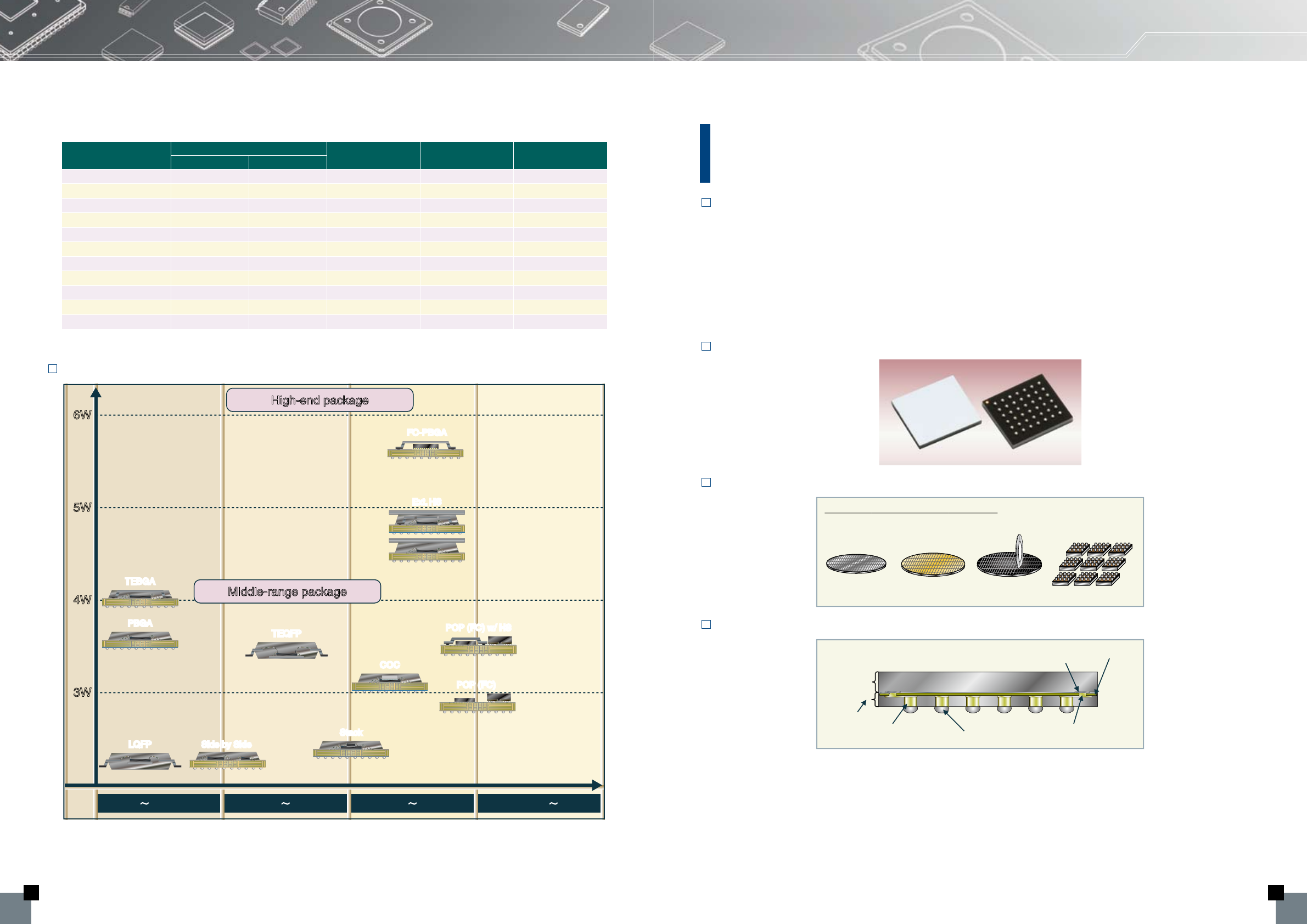
14
FC-CBGA
Please contact us for information on other pin arrangements.
■ Middle to High-end package road map
Fujitsu Semiconductor will provide the most suitable SiP to the customer's requirements with our extensive implementation technologies.
Please contact us for any requests.
Pin count Package size (mm) Pin arrangement Ball matrix Pin pitch (mm)
X Y
BGA625 27.0 27.0 Full Matrix 25 ×25 1.00
BGA625 33.0 33.0 Full Matrix 25 ×25 1.27
BGA729 35.0 35.0 Full Matrix 27 ×27 1.27
BGA900 31.0 31.0 Full Matrix 30 ×30 1.00
BGA900 40.0 40.0 Full Matrix 30 ×30 1.27
BGA1089 42.5 42.5 Full Matrix 33 ×33 1.27
BGA1156 35.0 35.0 Full Matrix 34 ×34 1.00
BGA1225 45.0 45.0 Full Matrix 35 ×35 1.27
BGA1369 37.5 37.5 Full Matrix 37 ×37 1.00
BGA1681 42.5 42.5 Full Matrix 41 ×41 1.00
BGA2116 47.5 47.5 Full Matrix 46 ×46 1.00
6W
5W
4W
3W
Middle-range package
High-end package
TEBGA
TEQFP
LQFP
PBGA
Side by Side
Stack
COC
POP (FC)
POP (FC) w/ HS
FC-PBGA
2008 2009 2010 2011 2012 2013
Ext. HS
IC-package_E.fm 14 ページ 2011年1月27日 木曜日 午後5時44分
IC Package
IC Package
15
WL-CSP
(Wafer Level CSP)
■ Features
Ultra compact, ultra thin, multi-pin, and superior humidity and reflow resistance by wafer consistent
assembly.
Also called as "Super CSP."
● Ultra compact, ultra thin, and light weight suitable for mobile devices and digital electric household appliances.
● JEDEC Moisture Sensitivity Level 1 clear.
● Support for pin pitch at less than or equal to 0.5mm contributing towards multi-pin.
● High speed transmission by reducing the wire length.
● Compliant with JEITA standards and fully customizable according to customer needs.
■ WL-CSP External view
■ WL-CSP Processes
■ WL-CSP Package cross section
WL-CSP
(Wafer Level CSP)
Process
Wafer Process Wafer Level Packaging
RDL Forming/
Encapsulation
Dicing
Al-pad
Solder Ball
Metal Post Cu Redistribution Line Cu
Polyimide
Encapsulant
Chip
IC-package_E.fm 15 ページ 2011年1月27日 木曜日 午後5時44分
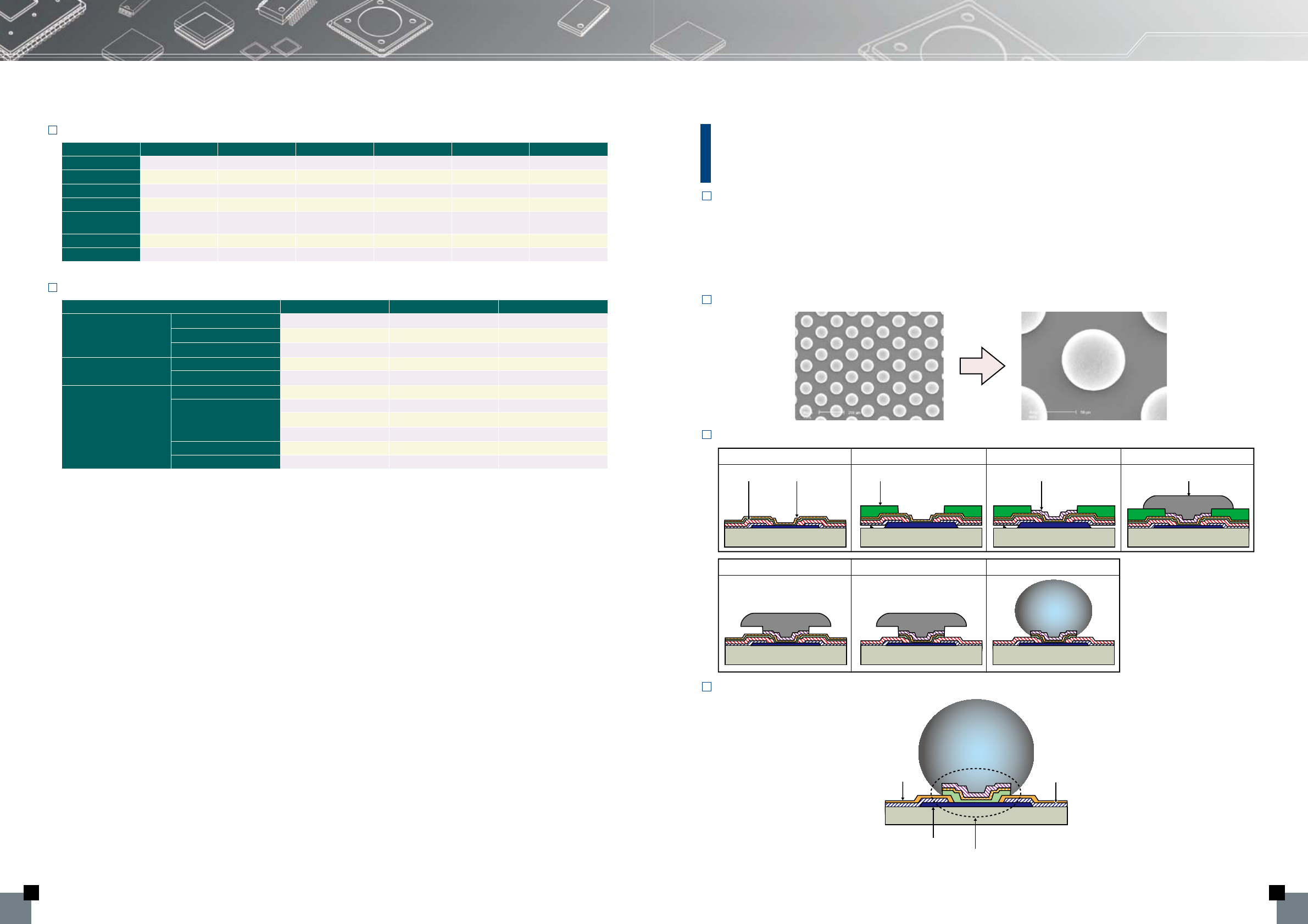
16
■ Mass-production actual performance
■ Technology road map
WL-CSP WLP112 WLP309 WLP15 WLP42 WLP70-02 WLP143
Wafer Size 200 mm 200 mm 200 mm 300 mm 300 mm 300 mm
Package Size 6.46 ×6.46 mm 7.56 ×7.56 mm 1.77 ×1.77 mm 3.30 ×2.95 mm 3.408 ×4.486 mm 7.81 ×6.10 mm
Package Height 0.6 mm Max 0.8 mm Max 0.64 mm Max 0.50 mm Max 0.35 mm Max 0.55 mm Max
Chip Thickness 390μm TYP 520μm TYP 390μm TYP 300μm TYP 220μm TYP 350μm TYP
Encapsulant
Thickness 50μm TYP 50μm TYP 50μm TYP 50μm TYP 50μm TYP 50μm TYP
Ball Pitch 0.5 mm 0.4 mm 0.4 mm 0.4 mm 0.4 mm 0.5 mm
Ball Height 110μm TYP 150μm TYP 150μm TYP 100μm TYP 100μm TYP 100μm TYP
2010 2011 2012
WL-CSP Structure
Height(Min)0.25 mm ← ←
Ball/Land pitch(Min)0.3 mm ← 0.25 mm
Ball/Land dia.(Min)0.15 mm ← 0.13 mm
RDL Technology Line/Space 20μm / 15μm←15μm / 15μm
Via/Land Pitch(Inline)50μm←40 μm
Others
Wafer size 6 / 8 / 12 inch ← ←
Scribe Width
(Min) 6/8in
12in
90μm ← ←
90μm(≦ 0.35-t)← ←
100μm(> 0.35-t)← ←
Solder Pb Free ← ←
Mold resin Halogen free ← ←
IC-package_E.fm 16 ページ 2011年1月27日 木曜日 午後5時44分
IC Package
IC Package
17
Bump on Pad
■ Features
Wafer process and bumping in consolidated assembly.
● Technology supporting wide range of products from low-end applications such as mobile devices and digital
electric household appliances to high-end applications such as servers.
● Promote multi-pin with min. 50μm AL pad pitch.
● Able to form wiring layer under a bump on demand.
■ Bump External view
■ Manufacturing process
■ Bump Cross section
(1) UBM Sputtering (2) Resist Patterning (3) UBM Plating (4) Bump Plating
(5) Resist removing (6) UBM etching (7) Bump shaping
Polyimide UBM Resist UBM (Plating) SnAg(Plating)
SnAg (Lead Free)
Polyimide Passivation
UBM (under barrier metal)
Al Pad
Si
IC-package_E.fm 17 ページ 2011年1月27日 木曜日 午後5時44分
18
■ Typical specification
■ Micro bump chip specification (example)
■ Mass-production actual performance
■ Technology road map
Wafer bumping A B C
Purpose High-end video 1seg tuner Image processing
Wafer size 300 mm 300 mm 300 mm
Chip size 9.52 ×14.44 mm 2.90 ×2.90 mm 5.10 ×4.50 mm
UBM size 0.080 mm 0.080 mm 0.200 mm
Bump height 0.085 mm 0.085 mm 0.100 mm
Bump pitch 0.176 mm 0.250 mm 0.400 mm
Chip thickness 0.550 mm 0.185 mm 0.450 mm
Bump material SnAg SnAg SnAg
(a) Bump pitch 176μm
(b) Bump height 85μm
(c) UBM size 80μm (typical)
(d) Passivation opening size 50μm (typical)
(e) Bump material SnAg (or PbSn)
(f) Chip thickness
(the thinnest case) 200μm
(b) (a)
(f)
(d)
(c)
(e) Solder Bump
(a)
(e) Solder Bump
(b)
(f) (d)
(c)
(a) Bump pitch 50μm
(b) Bump height 18μm
(c) UBM size 32μm (typical)
(d) Passivation opening size 17μm (typical)
(e) Bump material SnAg
(f) Chip thickness
(the thinnest case) 150μm
Standard bump
Pitch 150µm(Min)
UBM 85µm(Max)
Height 80µm(Max)
L&S 20/20µm(Min)
UBM 200µm(Max)
Height 100µm(Max)
L&S 15/20µm
UBM 200µm
Height 100µm
L&S 10/15µm
UBM 200µm
Height 100µm
Pitch 50µm(Min)
UBM 30µm(Min)
Height 18µm(Max)
UBM 200µm(Max)
Height 100µm(Max)
Pitch 40/30µm
UBM 20µm
Height 18µm
Pitch 130µm
UBM 85µm
Height 80µm
Pitch 100µm
UBM 70µm
Height 70µm
Micro bump
Bump package
Re-distribution
layer bump
2009 2010 2011 2012
IC-package_E.fm 18 ページ 2011年1月27日 木曜日 午後5時44分
IC Package
IC Package
19
■ Main package (Full scale: Size comparison)
FC-BGA 450pin ~ 2116pin
0.65mm Pitch 1.00mm Pitch
PBGA 256pin ~ 1156pin
1.00mm Pitch
QFP 100pin ~ 256pin
0.40mm Pitch 0.65mm Pitch
LQFP/TEQFP 48pin ~ 256pin
0.50mm Pitch QFN 16pin ~ 64pin
0.40mm Pitch
0.80mm Pitch
0.65mm Pitch
1.27mm Pitch
0.50mm Pitch
FBGA 66pin ~ 906pin
0.50mm Pitch
[Notation example]
625 㧦Pin count
(1717) 㧦Package size (unit:mm)
625
(1717)
1156
(3535)
1681
(42.542.5)
484
(2727)
676
(2727)
564
(3131)
1156
(3535)
320
(2727)
484
(3535)
256
(2828)
100
(1420)
48
(77)
100
(1414)
144
(2020)
208
(2828)
96
(66)
385
(1212)
753
(1818)
176
(1111)
385
(1616)
112
(1010)
240
(1515)
320
(1818)
20
(33)
56
(77)
32
(55)
64
(99)
IC-package_E.fm 19 ページ 2011年1月27日 木曜日 午後5時44分