Fujitsu Stacked/Multi Devices (Stacked MCP) Stackedmcp
User Manual: Fujitsu Stacked/Multi-Devices (Stacked MCP) Packaging ation - Fujitsu United States
Open the PDF directly: View PDF ![]() .
.
Page Count: 3
10
Advanced Packaging Services
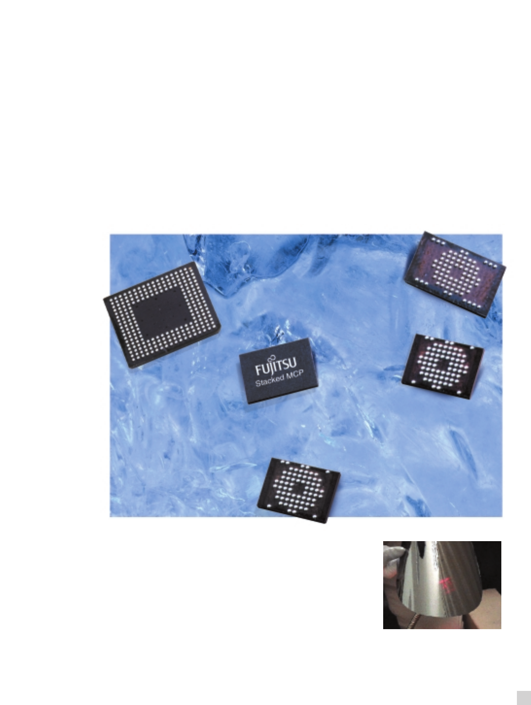
Stacked MCP
• Saves board space
• Ideal for integrating technologies or functions in one
single package
• Ideal for combining logic and memory at low cost
• Low profile
25µm Thin Wafer
Stacked Multi-Chip Package (Stacked MCP) is one of the most suitable chip scale packages for wireless
applications. Its advantage is the compact stacked chip configuration. In the Flash memory and SRAM
configuration, the pin layout can accomodate a 128 MB combination.Typical package construction
consists of two die back lapped down to 100µm and total package height is only 1.2 mm. Different
combinations of Flash and SRAM can be mounted in this package up to package size 10.4 x 10.8mm.
Stacked MCP supports packaging solutions up to 8 die stacked using flip-chip interconnection and
stacked wire bonded die. Additional logic-memory and logic-logic combinations are available.
11 Fujitsu Microelectronics America, Inc.
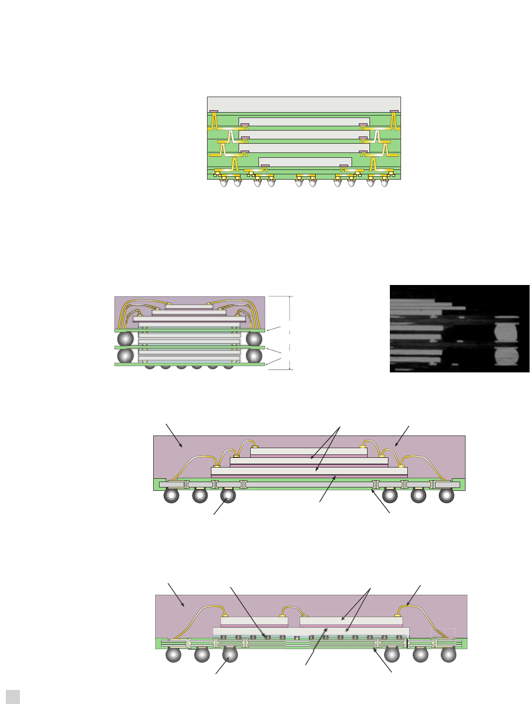
Stacked MCP
Di
e
A
u
Wir
e
Re
s
i
n
S
older Bal
l
Adhesive
S
ubstrat
e
Flip-chip bondin
g
Die Au Wire
Resin
Solder Ball Adhesive Substrate
3-chip stacked, wire bonding
Flip-chip bonding and wire bonding
8-chip stacked
Chip thickness:
50 µm (WB)
{
{
100 µm (FC)
4 metal-layer interposer
2 metal-layer interposer
2.0 mm max
5-chip stacked
The new module combines advances in wafer thinning technology, which reduces the thickness of existing chips
by about 16% , with chip stacking and re-distribution technologies. Compared to SiPs with similar
functionalities, the prototype chip boasts a 30% reduced board area and 65% thinner profile, making it the ideal
system LSI solution for miniaturized digital equipment.

12
Advanced Packaging Services
Stacked MCP
FBGA61 BGA-61P-M02 9 x 9 x 1.4 0.8 16M Flash + 2M SRAM
FBGA69 BGA-69P-M02 8 x 11 x 1.4 0.8 16M Flash + 4M SRAM
FBGA77 BGA-77P-M01 9 x 14 x 1.4 0.8 32M Flash + 4M SRAM
FBGA73 BGA-73P-M01 8 x 11.6 x 1.4 0.8 32M Flash + 2M SRAM
32M Flash + 4M SRAM
FBGA56 BGA-56P-M01 7 x 7.2 x 1.2 0.8 16M Flash + 2M SRAM
16M Flash + 4M SRAM
FBGA71 BGA-71P-M01 7 x 12 x 1.2 0.8 32M Flash + 8M SRAM
FBGA71 BGA-71P-M02 7 x 11 x 1.2 0.8 32M Flash + 16M SRAM
32M Flash + 4M SRAM
FBGA101 BGA-101P-M01 11 x 12 x 1.4 0.8 64M Flash + 8M SRAM
64M Flash + 16M FCRAM
FBGA123 BGA-123P-M01 11 x 12 x 1.4 0.8 64M Flash (NAND) + 16M FCRAM
FBGA81 BGA-81P-M03 10.4 x 10.8 x 1.2 0.8 64M Flash + 32M FCRAM
FBGA85 BGA-85P-M02 10.4 x 10.8 x 1.3 0.8 64M Flash + 16M FCRAM+ 4M SRAM
64M Flash (NAND) + 32M FCRAM+ 32 FCRAM
FBGA111 BGA-111P-M01 10.4 x 10.8 x 1.4 0.8 64M Flash (NAND) + 32M FCRAM
Package Type Package Code Body Size Pitch Configuration
(mm) (mm)
Standard Package Line-up
85°C/85%RH, 24 hours + IR250°C Pass
30°C/80%RH, 240 hours + IR250°C Pass
Condition Result
Moisture Sensitivity (FBGA69)
Thermal Performance (FBGA69)
Temperature Cycle* -65°C ~ 150°C 200 cycles Pass
HTS 150°C 1008 hours Pass
Thermal Shock 0°C ~ 100°C 200 cycles Pass
PTHS* 121°C, 85% 504 hours Pass
PTHB 121°C, 85% 96 hours Pass
Test Item Condition Criteria Result
* Preconditioning: Baking 125°C, 24 hours, +85°C ~ 85%, 20 hours + IR 250°C max.
45 40 35 10
θ-ja (°C/W) θ-jc (°C/W)
0m/sec 1m/sec 3m/sec
Package Reliability (FBGA69)
Custom configurations including non-memory applications are available.
