Futaba FDP03 2.4GHz Embedded Type Wireless Modem User Manual User s Manual
Futaba Corporation 2.4GHz Embedded Type Wireless Modem User s Manual
UserManual.wiki
>
Futaba
>
FDP03 User Manual
User's Manual
Navigation menu
Upload a User Manual
Namespaces
Wiki Guide
HTML
PDF
Info
Views
User Manual
Discussion / Help
Navigation
![Ver.1.0 4 2.2 Headerless Packet Transmission Mode By setting "Headerless packet transmission mode" on the REG03 register of the FDP03, the FDP03 transmits packets by wireless transmission to a destination address that is defined by the REG02 register. At this mode, a header part (command header "@", command "TXT" or "TBN", destination address, and number of message bytes [for TBN command]) can be eliminated. The trigger of data transmission can be defined by the setting of REG24 register. It can be selectable entering of "<Cr><Lf>" (0DH, 0AH) (i.e., carriage return and line feed codes) or time over of the timeout period (a time gap limit between two data bytes that is set in the REG26 register). Data transmission is triggered also when the number of message bytes exceeds 26 bytes. It is also enable to set "Enabling response" and "Disabling response" mode in by the REG13 register at the headerless packet transmission mode. Additionally, "Returning P1 and P0 responses" and "Returning P0 response" function can be selected when "Enabling response" mode is chosen. Moreover, "Enabling destination address check at reception" and "Disabling destination address check at reception" function can be selected by the REG18 register. For more details, see section 2.1 “Packet transmission mode”. Also, it is selectable whether "<Cr><Lf>" (0DH, 0AH) is added on the received data by the settings of the bit 4 of the REG23 register. In headerless packet transmission mode, maximum data buffer size for sending data is 150 bytes and data transmission is started when message data size exceeds 26 bytes. When many message data are input consequently, the message buffer may be overflowed and the message data may be lost. At that situation, the hardware flow control function should be set. If "Enabling response" function is selected in REG13 register, it is possible to judge whether data transmission is succeeded or not. Thus it is recommended to set "Enabling response" function even in headerless packet mode. Additionally, the massage data may be lacked when the size is over 26 bytes. To prevent for such an event, check each response on the sender and create messages so that the loss of packets can be detected on the receiver FDP03. The serial communication speed of all FDP03 should be same setting. If different serial communication speeds are set between on the sender and the receiver FDP03, data loss may occur on the slower speed side.](https://usermanual.wiki/Futaba/FDP03/User-Guide-1322173-Page-16.png)
![Ver.1.0 10 ⑧ ACK packet generation It is time for ACK packet generation. It takes 1.0 ms ⑨ ACK packet transmission It is time for ACK packet transmission that the acknowledgement of data packet reception. It takes 0.45 ms. ⑩ ACK reception processing It is processing time for ACK packet. It takes 1.0ms. ⑪ Serial output of received packet It is time for output of received data packet to the host 2 through the serial port. The time period depends on the communication setting between the host 2 and the receiver FDP03. If the transmission is text data at the packet transmission mode, size of output data packet is message bytes + 8 bytes because the header is 6 bytes and delimiter is 2 bytes. If the transmission is binary data at the packet transmission mode, size of send data packet is message bytes + 11 bytes because the header is 9 bytes and delimiter is 2 bytes. At the headerless packet mode, the data size is message bytes + 2 bytes if delimiter is included. On the other hand, if the trigger of transmission is “time-out”, the data size is the same as the message size. If "Adding '<Cr><Lf>' to received data" function of the receiver FDP03 is turned on by the bit 4 of REG23 (setting value is 1) at the headerless transmission mode, "<Cr><Lf>" is added at the end of the data and it consume 2 bytes. ⑫ Indication of data transmit completion A response is returned to the host 1when the data transmission is completed correctly. The length of response data is 4 bytes, and the time period of response return depends on the parameter settings of the communication parameters that are described in above section ①. Based on the above data processing flow, the total time for the data packet transmission from the host 1 to the host 2 can be calculated like below. (In the below calculation, no data packet re-transmission is supposed.) × 1000 × (size of message in bytes + A) + B + 6.4 × (C – 1) + × 1000 × (size of message in bytes + D) + 5.5 [ms] Expression 1 A: Text data is transmitted at packet transmission mode: 9 Binary data is transmitted at packet transmission mode: 12 Trigger of the data transmission is delimiter at headerless packet transmission mode: 2 Trigger of the data transmission is time-out at headerless packet transmission mode: 0 B: Trigger of the data transmission is time-out at headerless packet transmission mode: "Value of REG26" x 10 [If the bit 0 of REG24 is “1”] "Value of REG26" x 1 [If the bit 0 of REG24 is “0”] (*1) Others: 0 C: Data size of message is 0 to 26 bytes: 1 (*2) Data size of message is 27 to 52 bytes: 2 Data size of message is 53 to 78 bytes: 3 Data size of message is 79 to 104 bytes: 4 Data size of message is 105 to 103 bytes: 5 D: Text data is transmitted in packet transmission mode: 8 Binary data is transmitted in packet transmission mode: 11 Bit length per byte Line speed of the sender Bit length per byte Line speed of the receiver](https://usermanual.wiki/Futaba/FDP03/User-Guide-1322173-Page-22.png)
![Ver.1.0 11 Trigger of the data transmission is delimiter at headerless packet transmission mode: 2 Trigger of the data transmission is time-out at headerless packet transmission mode 0 *1 If the setting value is less than 3ms, the value of “B” will be “3”. *2 At headerless packet mode, the value of C is always 1. The total time until completion of the data transmission is calculated by below formula. × 1000 × (size of message in bytes + A + 4) + B + 6.4 × C + 1.5 Expression 2 A: Text data is transmitted at packet transmission mode: 9 Binary data is transmitted at packet transmission mode: 12 Trigger of the data transmission is delimiter at headerless packet transmission mode: 2 Trigger of the data transmission is time-out at headerless packet transmission mode: 0 B: Trigger of the data transmission is time-out at headerless packet transmission mode: "Value of REG26" x 10 [If the bit 0 of REG24 is “1”] "Value of REG26" x 1 [If the bit 0 of REG24 is “0”] (*1) Others: 0 C: Data size of message is 0 to 26 bytes: 1 (*2) Data size of message is 27 to 52 bytes: 2 Data size of message is 53 to 78 bytes: 3 Data size of message is 79 to 104 bytes: 4 Data size of message is 105 to 103 bytes: 5 *1 If the setting value is less than 3ms, the value of “B” will be “3”. *2 At headerless packet mode, the value of C is always 1. Bit length per byte Line speed of the sender](https://usermanual.wiki/Futaba/FDP03/User-Guide-1322173-Page-23.png)
![Ver.1.0 12 4.2 Time period of the case that data re-transmission of divided packet is occurred at packet transmission mode When packet data size is exceeding 26 bytes, it is divided into several packets that data size is 26 bytes. At that time, each divided packet is sent defined re-transmission times. Thus, maximum data transmission period will be (setting of REG11 register + 1) x 5 times. (REG11 register is a parameter of data re-transmission frequency.) It takes 7.6 ms if data transmission failure is occurred once. Therefore, total data processing time is like below formula. × 1000 × (size of message in bytes + A + 4) + B + 7.6 × frequency of data transmission Expression 3 A: Text data is transmitted at packet transmission mode: 9 Binary data is transmitted at packet transmission mode: 12 Trigger of the data transmission is delimiter at headerless packet transmission mode: 2 Trigger of the data transmission is time-out at headerless packet transmission mode: 0 B: Trigger of the data transmission is time-out at headerless packet transmission mode: "Value of REG26" x 10 [If the bit 0 of REG24 is “1”] "Value of REG26" x 1 [If the bit 0 of REG24 is “0”] (*) Others: 0 * If the setting value is less than 3ms, the value of “B” will be “3”. In this case, if data transmission failure is occurred in any given divided packet, following packets are not transmitted. Therefore, total data transmission period is fluctuated. Example 1: At the line speed set to 115,200 bps and bit length per byte set to 10 bits, time period of the data transmission failure detection is 53.1 ms if the first packet data is fail to transmit. (Size of the message is 130 bytes. Setting of data re-transmission frequency is 10 times.) (10/115,200) × 1,000 × (130 + 9 + 4) + 7.6 × (10+1) × 1 = 96.0 [ms] Example 2: At the line speed set to 115,200 bps and bit length per byte set to 10 bits, time period of the data transmission failure detection is 215.9 ms if the fifth packet data is fail to transmit. (Size of the message is 130 bytes. Setting of data re-transmission frequency is 10 times.) (10/115,200) × 1,000 × (130 + 9 + 4) + 7.6 × (10 + 1) × 5 = 430.4 [ms] As shown above, the total transmission time is largely fluctuated by the condition of the data transmission. To keep communication response well, size of the message should be less than 26 bytes. Bit length per byte Line speed of the sender](https://usermanual.wiki/Futaba/FDP03/User-Guide-1322173-Page-24.png)
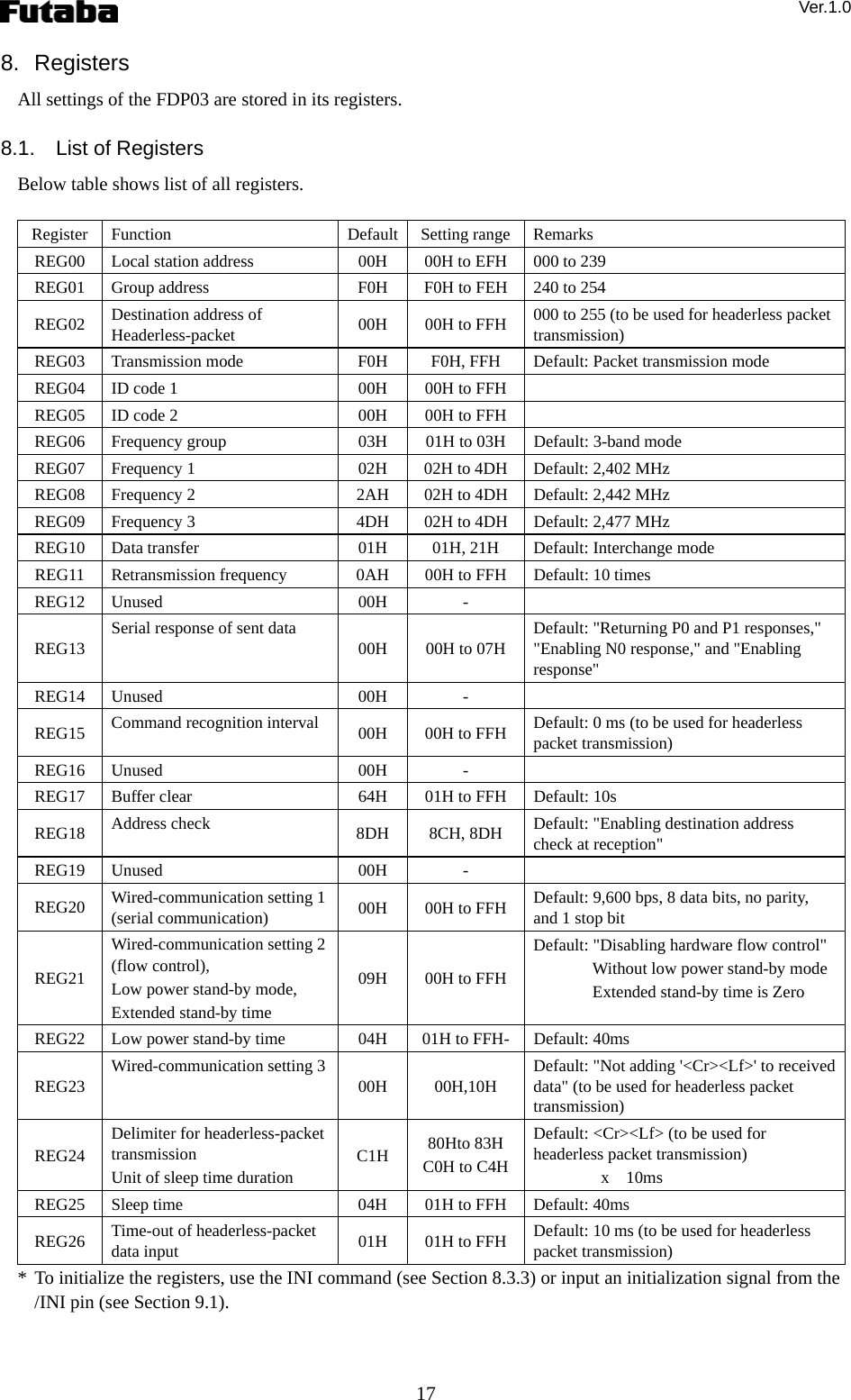
![Ver.1.0 18 8.2 Explanation of Registers REG00 (local station address) [Default: 00H] This register can set own wireless address. When the FDP03 receives a packet that destination is this address, the FDP03 processes the packet. The setting range is 00H to EFH (000 to 239). If the value is set to invalid range, the FDP03 returns N0 response. REG01 (group address) [Default: F0H] This is the wireless group address of the FDP03. When the FDP03 receives a packet that group is this address, the FDP03 processes the packet. If "Enabling destination address check at reception" function of the REG18 is turned on, the FDP03 returns ACK signal to sender FDP03 when it receives a packet. Therefore, if "Enabling destination address check at reception" function of all FDP03 in the system is turned on, all FDP03 that receive a packet return ACK signal. Thus, to avoid unnecessary communication, the REG18 may be set to "Disabling destination address check at reception". The range of the setting value is F0H to FEH (240 to 254). If the value is set to invalid range, the FDP03 returns N0 response. REG02 (headerless-packet destination address) (only for the headerless packet transmission mode) [Default: 00H] This register indicates the destination address of packet data in headerless packet transmission mode. This register also indicates the wireless address of the connection destination when TS2 command is used. The range of the setting value is 00H to FFH (000 to 255). If the value is set to invalid range, the FDP03 returns N0 response. REG03 (transmission mode) [Default: F0H] This register setting can change the transmission mode, which is packet transmission mode or headerless packet transmission mode. F0H Packet transmission mode (default) FFH Headerless packet transmission mode The value of the setting is F0H (packet transmission mode) or FFH (headerless packet transmission mode). If the value is set to invalid range, the FDP03 returns N0 response. REG04 (ID code 1) [Default: 00H] This register setting defines data scramble ID. Combined with ID code 2 (REG05), variation of data scramble ID is up to 65,536. Range of the setting value is 00H to FFH and FDP03 returns N0 response if the value is out of the range. The same scramble code (REG04 and REG05) must be set on all the FDP03s in the system. If the scramble codes are different each other, each FDP03 cannot communicate with.](https://usermanual.wiki/Futaba/FDP03/User-Guide-1322173-Page-30.png)
![Ver.1.0 19 REG05 (ID code 2) [Default: 00H] This register setting defines data scramble ID. Combined with ID code 1 (REG04), variation of data scramble ID is up to 65,536. Range of the setting value is 00H to FFH and FDP03 returns N0 response if the value is out of the range. The same scramble code (REG04 and REG05) must be set on all the FDP03s in the system. If the scramble codes are different each other, each FDP03 cannot communicate with. REG06 (frequency group) [Default: 03H] This register defines the number of frequencies to be used. 01H Use only the frequency set by REG07 02H Use the frequencies set by REG07 and REG08 03H Use the frequencies set by REG07 to REG09 (default) The range of settings is 01H to 03H. When the register is set to 01H, only a frequency that is set by REG07 is used. When the register is set to 02H, two frequencies that are set by REG07 and REG08 are used as a frequency group. When the register is set to 03H, three frequencies that are set by REG07 to REG09 are used as a frequency group. FDP03 returns N0 response if the value is out of the range. The setting value of REG07, REG08 and REG09 should not be duplicated when the setting of REG06 is “02H” and “03H”. If the frequencies have duplication, the transmission frequency will not be switched. REG07 (frequency 1) [Default: 02H] This register defines the frequency channel to be used for radio communication. The frequency channel that is set by this register is always used. The range of the setting is 2,402 MHz to 2,477 MHz. It is possible to set it by both 2-digital hexadecimal value (02H to 4DH) and 3-digit decimal value (002 to 077). For more details of correspondence between setting values and frequency channels, please refer section 5.1. FDP03 returns N0 response if the value is out of the range. REG08 (frequency 2) [Default: 2AH] This register defines the frequency channel to be used for radio communication. The frequency channel that is set by this register is applied when the RGE06 setting is 02H or 03H. The range of the setting is 2,402 MHz to 2477 MHz. It is possible to set it by both 2-digital hexadecimal value (02H to 4DH) and 3-digit decimal value (002 to 077). For more details of correspondence between setting values and frequency channels, please refer section 5.1. FDP03 returns N0 response if the value is out of the range.](https://usermanual.wiki/Futaba/FDP03/User-Guide-1322173-Page-31.png)
![Ver.1.0 20 REG09 (frequency 3) [Default: 4DH] This register defines the frequency channel to be used for radio communication. The frequency channel that is set by this register is applied only if the RGE06 setting is 03H. The range of the setting is 2,402 MHz to 2477 MHz. It is possible to set it by both 2-digital hexadecimal value (02H to 4DH) and 3-digit decimal value (002 to 077). For more details of correspondence between setting values and frequency channels, please refer section 5.1. FDP03 returns N0 response if the value is out of the range. REG10 (Data Transfer) [Default: 01H] Bit 7 and 6: Not used Bit 5: Data transfer mode 0 Interchange mode (default) 1 Communication Distance Extend mode The data transfer mode should be same setting among communication partners. If the mode is different each other, it is impossible to communicate with. Bit 4 to 0: Not used REG11 (retransmission count) [Default: 0AH] This register defines the maximum frequency of data packet retransmission. When the sender FDP03 cannot receive ACK signal from the receiver FDP03, it retransmits the data packet "'defined value of this register' +1" times. At broadcast transmission mode, the sender FDP03 always sends the data packet "'defined value of this register' +1" times. The enable setting range of this register is 00H to FFH (0 to 255 times). FDP03 returns N0 response if the value is out of the range. REG12 (unused) [Default: 00H] This register is not used. It should be default setting “00H”.](https://usermanual.wiki/Futaba/FDP03/User-Guide-1322173-Page-32.png)
![Ver.1.0 21 REG13 (Serial response to packet input) [Default: 00H] This register defines the responses for in-coming data packet from the host through the serial port. Bits 7 to 3: Not used Bit 2: N0 response 0 Enabling N0 response (default) 1 Disabling N0 response Bit 2 is available only if the bit 0 is set to "Enabling response." If this bit is set to “0” (Enabling N0 response), the FDP03 sends N0 response to the host thorough the serial port when the packet data format from the host is invalid or time gap between bytes is more than 5 seconds. If this bit is set to “1”, the FDP03 does not send any N0 response to the host . When the bit2 of REG13 is set to “1”, the FDP03 does not send any response even if the packet format is invalid. Bit 1: Normal response 0 Returning P0 and P1 responses (default) 1 Returning P0 response Bit 1 is available only if the bit 0 is set to "Enabling response." By this setting, it is possible to select type of response when the data packet configuration is valid. If the bit 1 is set to “0”, the FDP03 sends P1 response to the host through the serial port when it receives a data packet. Also, it sends P0 response to the host when the data transmission to the receiver is success. When the data transmission to the receiver is failed, the FDP03 sends N1 response to the host. If the bit 1 is set to “1”, the FDP03 sends P0 response to the host through the serial port when the data transmission to the receiver is success and sends N1 response when the data transmission to the receiver is failed. Bit 0: Enabling response 0 Enabling response (default) 1 Disabling response The bit 0 is defines whether the FDP03 send a response to the host or not. When bit 0 is set to 0, the FDP03 sends particular specified responses to the host through the serial port. When bit 0 is set to 1, the FDP03 does not send any response to the host. When the 0 is set to “1”, the FDP03 does not send any response even if the packet configuration is invalid. During the register setting, the FDP03 always sends the responses if it is any settings.](https://usermanual.wiki/Futaba/FDP03/User-Guide-1322173-Page-33.png)
![Ver.1.0 22 REG14 (unused) [Default: 00H] This register is not used. It should be default setting “00H”. REG15 (command recognition interval) (only for the headerless packet transmission mode) [Default: 00H] If the packet to be transmitted in headerless packet transmission mode includes code "40H", which indicates the command header (@), the data following the code is handled as a command, and the packet cannot be transmitted normally. This register is used to avoid such problems. Code "40H" is handled as the command header only when the code is input after a time gap between bytes that exceeds the value set in this register. The range of settings is 00H to FFH. The value is in units of 100 ms. With the default setting (00H) of this register, code "40H" is always handled as the command header. REG16 (unused) [Default: 00H] This register is not used. It should be default setting “00H”. REG17 (unused) [Default: 64H] This register is not used. It should be default setting “00H” REG18 (address check) [Default: 8FH] Bits 7 to 2: Not used Bit 1: Group address check 0 Disabling group address check at reception 1 Enabling group address check at reception (default) Only if the bit 0 of REG18 is 0, the bit 1 is available. When the bit 1 is set to “0”, the FDP03 receives all data packets whatever the destination address of the data packet is. On the other hand, the FDP03 only receives the data packets that destination address is consistent. The FDP03 does not return ACK signal to the senders at both settings. Bit 0: Destination address check 0 Disabling destination address check at reception 1 Enabling destination address check at reception (default) When the bit 0 is set to 0, the FDP03 receives all data packets whatever the destination address of the data packet is. At this setting, the FDP03 does not send back any ACK signal. When the bit 0 is set to 1, the FDP03 checks the destination addresses of data packets and receives only if the destination address is consists with its wireless address. At this setting, the FDP03 returns ACK signal to the host.](https://usermanual.wiki/Futaba/FDP03/User-Guide-1322173-Page-34.png)
![Ver.1.0 23 REG19 (unused) [Default: 00H] This register is not used. It should be default setting “00H”. REG20 (wired-communication setting 1) (serial communication) [Default: 00H] Bit 7: Data length 0 8 bits (default) 1 7 bits Bit 6: Enabling parity 0 No parity (default) 1 Using parity Bit 5: Type of parity 0 Even parity (default) 1 Odd parity Bit 4: Stop bit 0 1 bit (default) 1 2 bits Bits 3 and 2: Not used Bits 1 and 0: Baud rate Bit 1 Bit 0 Baud rate 0 0 9,600 bps (default) 0 1 19,200 bps 1 0 38,400 bps 1 1 115,200 bps](https://usermanual.wiki/Futaba/FDP03/User-Guide-1322173-Page-35.png)
![Ver.1.0 24 REG21 (wired-communication setting 2[flow control], low power stand-by mode, extended stand-by time) [Default: 09H] Bits 7 to 4: Extended Stand-by time Bit 7 Bit 6 Bit5 Bit4 Extended Stand-by time 0 0 0 0 0 (0x20): Default 0 0 0 1 20ms (1x20) 0 0 1 0 40ms (2x20) . . . 1 1 1 0 280ms (14x20) 1 1 1 1 300ms (15x20) When the FDP03 receives data packet that destination address is matched at the setting of the REG18 is “Enabling destination address check at reception”, the time duration of the Stand-by mode is extended. If the data packet is set by broadcasting mode and/or the setting of the REG18 is “Disabling group address check at reception”, the time duration of the Stand-by mode is NOT extended. When “Extended Stand-by time” is set to 0ms, the FDP03 becomes “Sleep” mode right after it sends back ACK packet. Bit 3: No used Bit 2: Low power stand-by mode 0 Normal Operation Mode (Default) 1 Low Power Stand-by Mode By setting “1” for the bit 2 of REG21 and re-booting the FDP03, operation mode becomes “Low power stand-by mode”. It is also turned “low power operation mode” after returning from the “Power down mode”. Time duration of the Stand-by and sleep mode are set by REG22 and REG25, respectively. Bit 1: Hardware flow control 0 Disabling hardware flow control (default) 1 Enabling hardware flow control This register can define validity of hardware flow control. If hardware flow control is enabled, the setting of the FDP03 should be same as that of the external device that connected to the FDP03. On the FDP03, make the same setting of this register as the flow control setting on the external equipment connected to the FDP03. Hardware flow control is available by connecting control cables to the RTS and CTS pins. Data flow may not stop immediately right after the hardware flow control vans the data flow if the software is written by PC. In such a case, some data from the PC may be lost. Bit 0: Not used](https://usermanual.wiki/Futaba/FDP03/User-Guide-1322173-Page-36.png)
![Ver.1.0 25 REG22 (Low power stand-by time) [Default: 04H] This register can define time duration of low power stand-by mode. The available setting value is 1 (10ms) to 255 (2550ms). Default value is 4 (40ms). “Low power stand-by time” should be longer than 30ms when 2 frequency channel mode is used. Also, it should be longer than 40ms when 3 frequency channel mode is used. When “Re-transmission count” (REG11) is large, data communication is sometimes failed. Especially, if the data message is divided into some packets, possibility of communication failure increases. REG23 (wired-communication setting 3) (only for the headerless packet transmission mode) [Default: 00H] Bits 7 to 5: Not used Bit 4: Enable addition of <Cr><Lf> to the received data 0 Not add '<Cr><Lf>' to the received data (default) 1 Add '<Cr><Lf>' to the received data This register defines availability of "<Cr><Lf>" (carriage return and line feed codes) addition to the end of the received data when the setting value of REG03 is “FFH”. Bits 3 to 0: Not used REG24 (delimiter for headerless-packet transmission, Unit of sleep time duration) [Default: C1H] Bit 7: Not used Bit 6: Delimiter 0 Time-out 1 <Cr><Lf> (default) This bit of the register defines the trigger of data transmission when the setting value of REG03 is “FFH”. When the value of the bit 0 is “0”, the FDP03 starts transmission if no data packet is coming during specific time that is defined by REG26. Bits 5 to 2: Not used Bit 1: Unit of sleep time duration 0 x 10ms (Default) 1 x 100ms Bit 0: Unit of time-out time 0 x 1 ms 1 x 10 ms (Default) The time-out time is defined by this bit and REG26.](https://usermanual.wiki/Futaba/FDP03/User-Guide-1322173-Page-37.png)
![Ver.1.0 26 REG25 (Sleep time) [Default: 04H] This register can define the time duration of the sleep mode. Available setting value is 1 to 255. The unit of this setting is defined by bit1 of REG24. (x 10ms or x 100ms). Initial setting is 4 (40ms or 400ms). This time setting is available when the low power stand-by mode is set by PON command. REG26 (time-out of headerless-packet data input) [Default: 01H] This register is available when the transmission mode is headerless packet mode (setting value of REG03 is “FFH”) and the trigger of the data transmission is time-out (the bit 6 of the REG24 is set to “0”). The data packet is transmitted if no data packet is coming during set time by the REG24 and the REG26. If the bit 0 of the REG24 is set to “0”, the unit of this time set is 1 ms. Similarly, if the bit 0 of the REG24 is set to “1”, the unit of this time set is 10 ms. Available value of the setting is from 01H to FFH, 0 to 255. However, minimum time duration is 3 ms even if the setting is below 3 ms. The FDP03 returns N0 response if “00H” is set to the value.](https://usermanual.wiki/Futaba/FDP03/User-Guide-1322173-Page-38.png)
![Ver.1.0 30 9.3.3 Explanation of commands ARG (Show all registers) [Format] ARG [Response] List of register settings (REG00 to REG26) N0: Command error [Function] - The FDP03 returns all register settings by this command. - The register settings are shown in hexadecimal code. [Examples of use] >@ARG<Cr><Lf> <REG00: 00H<Cr><Lf> <REG01: F0H<Cr><Lf> ・ ・ ・ <REG26: 01H<Cr><Lf> BCL (Clear transmission and reception buffers) [Format] BCL [Response] P0: Normal end N0: Command error [Function] - The transmission and reception buffer is cleared by this command. [Examples of use] >@BCL<Cr><Lf> <P0<Cr><Lf> If this command is executed during data transmission in broadcast transmission mode, newly in coming data might be stored and output after the buffer is cleared. Also, serial data output is stopped when this command is executed during serial data output.](https://usermanual.wiki/Futaba/FDP03/User-Guide-1322173-Page-42.png)
![Ver.1.0 31 DAS (Show/set the destination address) [Format] DAS (setting value) setting value: 000 to 255 [Response] xxx: Current address (in case of address referencing) P0: Normal end (in case of address setting) N0: Command error [Function] - This command shows and/or sets the destination address of headerless packet transmission mode. - When this command is entered without any setting values, the FDP03 returns current destination address. If setting value (new address) is put after DAS command, the destination address of the FDP03 is changed to new one. - Setting of a new address by this command is temporary. If the FDP03 is reset by RST command or initialized, the destination address is returned to the address that is defined by REG02. [Examples of use] >@DAS<Cr><Lf>: Show current destination address <003<Cr><Lf>: Current destination address is “003”. >@DAS001<Cr><Lf>: Set the destination address to “001”. <P0<Cr><Lf>: The destination address is changed normally.](https://usermanual.wiki/Futaba/FDP03/User-Guide-1322173-Page-43.png)
![Ver.1.0 32 FNU (Show/set a frequency group) [Format] FNU (frequency-group) Available “frequency-group”: 1 to 3 [Response] x: Currently set value P0: Normal end N0: Command error [Function] - This command shows or sets the frequency group. - When this command is executed without setting value, current value is recalled. - Available setting value "x" is 1 to 3. "1" indicates 1 channel mode (fixed frequency channel), "2" means 2 channel mode, and "3" represents 3 channel mode. - Frequency group setting by this command is temporary. Thus, the setting is returned to that of REG06 after executing RST command or resetting FDP03. For permanent setting, the REG06 should be changed. “x” (Setting Va lu e ) Description 1 1 channel mode. Frequency channel that defined by REG07 is used. 2 2 channel mode. Frequency channels that defined by REG07 and REG08 are used. 3 3 channel mode. Frequency channels that defined by REG07, REG08 and REG09 are used. [Examples of use] >@FNU<Cr><Lf>: This command recalls the current set frequency group. <3<Cr><Lf>: This response indicates the current set value is "3" (3-band mode). >@FNU1<Cr><Lf>: This command sets the frequency group to the 1-band mode (1). <P0<Cr><Lf>: This response indicates the normal end of command processing.](https://usermanual.wiki/Futaba/FDP03/User-Guide-1322173-Page-44.png)
![Ver.1.0 33 FRQ (Show/set frequency channel) [Format] FRQ (number) (:frequency channel) Available “number”: 1 to 3 Available “frequency channel”: 02 to 77 [Response] yy: Current frequency channel (02 to 77) P0: Normal end N0: Command error [Function] - This command indicates or sets a frequency channel. - When this command is executed without “frequency channel”, current frequency channel is recalled. - Frequency channel setting by this command is temporary. Thus, the setting is returned to that of REG07, REG08 and REG09 after executing RST command or resetting FDP03. For permanent setting, the REG07, REG08 and REG09 should be changed. Available setting value of "number" is 1 to 3. "1" indicates the frequency channel set of REG07, "2" indicates the frequency channel set of REG08, and "3" indicates the frequency channel set of REG09. “number” Description 1 Frequency channel of REG07 2 Frequency channel of REG08 3 Frequency channel of REG09 [Examples of use] >@FRQ1<Cr><Lf>: This command recalls the frequency channel of “frequency cannel 1”. <02<Cr><Lf>: This response indicates the current t frequency channel is 02 (2,402MHz). >@FRQ2:15<Cr><Lf>: This command sets the “frequency channel 2” to channel “15” (2,415MHz). <P0<Cr><Lf>: This response indicates the normal end of command processing.](https://usermanual.wiki/Futaba/FDP03/User-Guide-1322173-Page-45.png)
![Ver.1.0 34 IDR (Show ID code) [Format] IDR [Response] xxxxH: Current setting value (It is the value of REG04 and REG05 right after turned ON the main power.) [Function] - This command shows the ID code. [Example of use] >@IDR<Cr><Lf>: This command shows the ID code. <0000H<Cr>Lf>: This response indicates the current ID code is “0000H”. IDW (Set ID code) [Format] IDW Available setting value: “0000H” to “FFFFFH” [Response] P0: Normal end N0: Command error [Function] - This command can change ID code temporarily. For permanent change, REG04 and REG05 should be changed. [Example of use] >@IDW1234H<Cr><Lf>: This command set ID code to 1234. <P0<Cr>Lf>: Normal end.](https://usermanual.wiki/Futaba/FDP03/User-Guide-1322173-Page-46.png)
![Ver.1.0 35 INI (initializing memory registers) [Format] INI [Response] P0: Normal end N0: Command error [Function] - This command resets all memory registers of the FDP03 to initial settings. - All register settings that are customized are vanished. [Example of use] >@INI<Cr><Lf>: This command initializes all memory registers. <P0<Cr>Lf>: This response indicates the normal end of command processing. The host cannot receive any response from the FDP03 if a communication parameters such as baud rate are different from default setting. It will take 520ms at maximum for P0 response of this command. Memory registers may get damages if the power of FDP03 is turned off before the P0 response comes back.](https://usermanual.wiki/Futaba/FDP03/User-Guide-1322173-Page-47.png)
![Ver.1.0 36 REG (Show/set memory registers) [Format] REG (register-number) (:setting value) register-number: 00 to 26 setting value: 00H to FFH (000 to 255) [Response] xxH: Current value P0: Normal end N0: Command error [Function] - This command recalls setting value of memory register and/or sets a value of memory register. - Available setting value of “register number” is 00 to 26. - When this command is executed without “setting value”, current value of the defined register is recalled. - “setting value” should be 3 digit decimal value or 2 digit hexadecimal value . If it is hexadecimal value, “H” should be added at the end of the value. [Examples of use] >@REG00<Cr><Lf>: This command recalls the value of REG00. <00H<Cr><Lf>: This response indicates the current value is “00H”. >@REG00:001<Cr><Lf>: This command sets value of REG00 to 001 <P0<Cr><Lf>: This response indicates the normal end of command processing. After executing this command to set a new value for a register, be sure to execute the RST command. If you turn off the power of the FDP03 before executing the RST command, the new setting of the register will not be reflected to the FDP03. It will take 520ms at maximum for P0 response of this command.](https://usermanual.wiki/Futaba/FDP03/User-Guide-1322173-Page-48.png)
![Ver.1.0 37 RST (resetting the FDP03) [Format] RST [Response] P0: Normal end N0: Command error [Function] - This command has the following two functions: (1) If values of the memory registers are changed before this command is executed, new register settings are registered by this command execution. However, values that are changed by “DAS”, “FUN” and “FRQ” command are vanished and the settings of memory registers are effective. (2) This command also makes the FDP03 exit from the line quality test of the “TS2” command. When this command is executed for exit from the line quality test, the memory register settings that are made before execution of the TS2 command are not saved. [Example of use] >@RST<Cr><Lf>: This command resets the FDP03. <P0<Cr><Lf>: This response indicates the normal end of command processing. The host cannot receive any response from the FDP03 if communication parameters such as baud rate are different from default setting. It will take 520ms at maximum for P0 response of this command. Memory registers may get damages if the power of FDP03 is turned off before the P0 response comes back.](https://usermanual.wiki/Futaba/FDP03/User-Guide-1322173-Page-49.png)
![Ver.1.0 38 POF (Release low power stand-by mode) [Format] POF [Response] P0: Normal end N0: Command error [Function] - The operation mode is returned from “Low power stand-by mode” to “Normal operation mode” by this command. [Example of use] >@POF<Cr><Lf>: Release low power stand-by mode. <P0<Cr>Lf>: Normal end. N0 response is returned if this command is executed during normal operation mode. PON (Set low power stand-by mode) [Format] PON [Response] P0: Normal end N0: Command error [Function] - The operation mode is set to “Low power stand-by mode.. [Example of use] >@PON<Cr><Lf>: Set low power stand-by mode. <P0<Cr>Lf>: Normal end. N0 response is returned if this command is executed during low power stand-by mode.](https://usermanual.wiki/Futaba/FDP03/User-Guide-1322173-Page-50.png)
![Ver.1.0 39 PTE (Show/Set extended stand-by time) [Format] PTE(:setting value) Available setting value: 000 to 015 [Response] xxx: Current setting value (as referring the value) P0: Normal end (as setting the value) N0: Command error [Function] - This command can refer and/or set the time duration of the extended stand-by time. The extended stand-by time duration is the setting value of this command times 20ms. For example, if the setting value is 010, the extended stand-by time duration is 200ms (010 x 20ms). If the setting value is 000, the extended stand-by time is not available. [Example of use] >@PTE<Cr><Lf>: Show current setting value <003<Cr>Lf>: The setting value is 003. It means that the extended stand-by time duration is 60ms (003 x 20ms). >@PTE015<Cr><Lf>: Set the extended stand-by time duration to 300ms (015 x 20ms). <P0<Cr><Lf> : Normal end. If the data packet is sent by broadcasting mode and/or the address check function (REG18) setting is “Disabling group address check at reception”, the FDP03 does not turn to the “Extended Stand-by mode” even if the extended time duration is set. PTN (Show/Set stand-by time) [Format] PTN(:setting value) Available setting value: 001 to 255 [Response] xxx: Current setting value (as referring the value) P0: Normal end (as setting the value) N0: Command error [Function] - This command can refer and/or set the time duration of the stand-by time. During the stand-by time, the RF circuit is turned on. The stand-by time duration is the setting value of this command times 10ms. For instance, if the setting value is 010, the extended stand-by time duration is 100ms (010 x 10ms). [Example of use] >@PTN<Cr><Lf>: Show current setting value <003<Cr>Lf>: The setting value is 005. It means that the stand-by time duration is 50ms (005 x 10ms). >@PTN007<Cr><Lf>: Set the extended stand-by time duration to 70ms (007 x 10ms). <P0<Cr><Lf> : Normal end.](https://usermanual.wiki/Futaba/FDP03/User-Guide-1322173-Page-51.png)
![Ver.1.0 40 PTS (Show/Set sleep time) [Format] PTS(:setting value) Available setting value: 001 to 255 [Response] xxx: Current setting value (as referring the value) P0: Normal end (as setting the value) N0: Command error [Function] - This command can refer and/or set the time duration of the sleep time. The sleep time duration is the setting value of this command times 10ms if the setting of bit 1 of RGE24 is “0”. Also, it is the setting value of this command times 100ms if the setting of bit 1 of RGE24 is “1”. For example, if the setting value is 030 and the setting of bit 1 of REG24 is “0”, the sleep time duration is 30ms (030 x 10ms). If the setting value is 050 and the setting of bit 1 of REG24 is “1”, the sleep time duration is 500ms (050 x 100ms). [Example of use] >@PTS<Cr><Lf>: Show current setting value <025<Cr>Lf>: The setting value is 025. It means that sleep time is 250ms (as bit 1 of REG24 is “0”) or 2500ms (as bit 1 of REG24 is “1”). >@PTS010<Cr><Lf>: Set the sleep time duration to 100ms (as bit 1 of REG24 is “0”) or 1000ms (as bit 1 of REG24 is “1”). <P0<Cr><Lf> : Normal end. ROF (RF circuit OFF) [Format] ROF [Response] P0: Normal end N0: Command error [Function] - This command turns off the RF circuit. If the RF circuit has been already turned off, N0 response is returned after executing this command. [Example of use] >@ROF<Cr><Lf>: Turn off the RF circuit. <P0<Cr><Lf> : Normal end. During the RF circuit is turned off, @TXT and @TBN command are not available.](https://usermanual.wiki/Futaba/FDP03/User-Guide-1322173-Page-52.png)
![Ver.1.0 41 RON (RF circuit ON) [Format] RON [Response] P0: Normal end N0: Command error [Function] - This command turns on the RF circuit. If the RF circuit has been already turned on, N0 response is returned after executing this command. [Example of use] >@RON<Cr><Lf>: Turn on the RF circuit. <P0<Cr><Lf> : Normal end. SPD (Show/set data transfer mode) [Format] SPD(: Data transfer mode) Data transfer mode: 1 or 2 [Response] x: Current setting value P0: Normal end N0: Command error [Function] - This command show and/set data transfer mode. - The data transfer mode is “Interchange” mode if the setting value is “1”. - The data transfer mode is “Communication Distance Extend” mode if the setting value is “2”. - Setting of the data transfer mode by this command is temporary. If the FDP03 is reset by RST command or initialized, the mode is returned to the setting of the bit 5 of the REG10. x (Setting Value) Data Transfer Mode 1 Interchange Mode 2 Communication Distance Extend Mode [Example of use] >@SPD<Cr><Lf>: Show the data transfer mode. <1<Cr><Lf> : The mode is “Interchange” mode. >@SPD2<Cr><Lf>: Set the data transfer mode to “Communication Distance Extend” mode. <P0<Cr><Lf> : Normal end. The data transfer mode should be same setting among communication partners. If the mode is different each other, it is impossible to communicate with.](https://usermanual.wiki/Futaba/FDP03/User-Guide-1322173-Page-53.png)
![Ver.1.0 42 TBN (transmit binary data) [Format] TBN (destination-address) (length-of-message-bytes) (message) - destination-address: 000 to 239 240 to 254 (for group communication) 255 (for broadcast transmission) - length-of-message-bytes: 000 to 130 - message: Arbitrary binary data (130 bytes or less) [Response] P0: Normal end P1: Command is accepted and data are being transmitted N0: Command error N1: Data transmission is failed. (The radio modem at the destination address does not respond or transmission cannot be started because of carrier sensing.) N3: Data transmission is failed because the receiving data buffer of the destination modem is full. [Function] - This command transmits binary data. - The length of message can be defined from 0 to 130 bytes arbitrary. - To broadcast data to multiple radio modems, “destination address” should be defined to “255”. At this setting, the sender FDP03 transmits data packet “re-transmission frequency” that is defined by REG11 + 1 times and then returns P1 and/or P0 response to the host according to the REG13 setting. [Examples of use] >@TBN001005HELLO<Cr><Lf>: The FDP03 sends the message “HELLO” to the destination modem that wireless address is “001” by this command. <P1<Cr><Lf>: This response indicates that the command is accepted and the data is being transmitted. <P0<Cr><Lf>: This response indicates the normal end of command processing. >@TBN002005HELLO<Cr><Lf>: The FDP03 sends the message “HELLO” to the destination modem that wireless address is “002” by this command. <P1<Cr><Lf>: This response indicates that the command is accepted and the data is being transmitted. <N1<Cr><Lf>: This response indicates that transmission is failed because the destination modem that wireless address is “002” did not respond or the data transmission was not started by carrier sensing. The length of message should be not more than 130 bytes. It becomes command error if the length of message exceeds 130 bytes. The delimiter of this command should be “<Cr><Lf>”. It becomes command error if different delimiter is added. At broadcast transmission mode, the sender FDP03 cannot recognize whether receiver FDP03s receive the transmitted data or not. Do NOT execute next command before the sender FDP03 receives P0 response. If the setting is "Disabling response" and no P0 response is sent to the sender FDP03, please wait expected P0 response time before executing next command. If next command is executed before P0 response, command error is occurred and the system might have unexpected movement.](https://usermanual.wiki/Futaba/FDP03/User-Guide-1322173-Page-54.png)
![Ver.1.0 43 TID (show the serial number) [Format] TID [Response] xxxxxxxxx: 9-digit serial number N0: Command error [Function] The FDP03 replies its 9 digits serial number when this command is executed. If it is failed to read the serial number, the FDP03 returns “?”. [Example of use] >@TID<Cr><Lf>: This command requests to show the serial number of the FDP03. < xxxxxxxxx <Cr><Lf>: This response indicates the serial number of the FDP03. TS2 (executing a communication line quality test) [Format] TS2 [Response] P0: Command accepted Connect: Line connected and line quality test is started ooooo....ooxo 003: Test result Disconnect: Line disconnected N0: Command error [Function] - The communication line quality test is executed by this command. At the test, one data packet has 32 bytes and one hundred packets are exchanged as a test unit between the “master” FDP03 and the “slave” FDP03. The test results are output to the serial port. - The test result is shown by “o” and “x” for each packet. “o” indicates that it is no communication error and “x” indicates that communication error is occurred. - When this command is executed at the “master” FDP03, the “master” tries to connect the “slave” FDP03 that wireless address is defined by REG02 of the “master”. At that time, operation mode of the “slave” is automatically changed to TS2 communication line quality test mode. - Both the “master” and the “slave” output the test result. - Total error occurrence of the test is indicated in 3 digits number after 100 of “o” ”x” judgments. - If consecutive 1,000 packets become communication error, the line is disconnected. After the disconnection, the “master” continues to request wireless connection but the “slave” abort from TS2 test mode. - During this TS2 test mode, all the commands except for “FUN”, “FRQ” and “RST” command are do not work. For abort from TS2 test mode, it is needed to execute “RST” command or turned off the main power of the FDP03. When the “master” aborts from TS2 test mode, the “slave” automatically stops the test mode and returns to normal operation mode. [Example of use] >@TS2<Cr><Lf>: The FDP03 runs communication test by this command. <P0<Cr><Lf>: This response indicates that the command is accepted. <Connect<Cr><Lf>: This response indicates that the line is connected. <xooooooooo...ooox 003<Cr><Lf>: This response indicates the test result and 3 packets became communication errors during 100 packet correspondences. <oooxoooooo...oxoo 002<Cr><Lf>: This response indicates the test result and 2packets became communication errors during 100 packet correspondences. <oooooooxxo...ooxo 004<Cr><Lf>: This response indicates the test result and 4 packets became communication errors during 100 packet correspondences. <ooxxxooooo...oxoo 006<Cr><Lf>: This response indicates the test result and 6 packets became communication errors during 100 packet correspondences.](https://usermanual.wiki/Futaba/FDP03/User-Guide-1322173-Page-55.png)
![Ver.1.0 44 TXT (transmit text data) [Format] TXT (destination-address) (message) - destination-address: 000 to 239 240 to 254 (for group communication) 255 (for broadcast transmission) - message: Arbitrary binary data (130 bytes or less) [Response] P0: Normal end P1: Command is accepted and data are being transmitted N0: Command error N1: Data transmission is failed. (The radio modem at the destination address does not respond or transmission cannot be started because of carrier sensing.) [Function] - This command orders the FDP03 to transmit text data. - The length of message can be defined from 0 to 130 bytes and a delimiter indicates the end of message data. - To broadcast data to multiple radio modems, “destination address” should be defined to “255”. At this setting, the sender FDP03 transmits data packet “re-transmission frequency” that is defined by REG11 + 1 times and then returns P1 and/or P0 response to the host according to the REG13 setting. [Examples of use] >@TXT001HELLO<Cr><Lf>: The FDP03 sends the message “HELLO” to the destination modem that wireless address is “001” by this command. <P1<Cr><Lf>: This response indicates that the command is accepted and the data is being transmitted. <P0<Cr><Lf>: This response indicates the normal end of command processing. >@TXT002HELLO<Cr><Lf>: The FDP03 sends the message “HELLO” to the destination modem that wireless address is “002” by this command. <P1<Cr><Lf>: This response indicates that the command is accepted and the data is being transmitted. <N1<Cr><Lf>: This response indicates that transmission is failed because the destination modem that wireless address is “002” did not respond or the data transmission was not started by carrier sensing. The length of message should be not more than 130 bytes. It becomes command error if the length of message exceeds 130 bytes. If the message includes "<Cr><Lf>," the FDP03 is recognizes that it is the end of the message and it ignores following message. Thus, “TBN” command should be used instead of “TXT” command if the message contains “<Cr><Lf>”. At broadcast transmission mode, the sender FDP03 cannot recognize whether receiver FDP03s receive the transmitted data or not. Do NOT execute next command before the sender FDP03 receives P0 response. If the setting is "Disabling response" and no P0 response is sent to the sender FDP03, please wait expected P0 response time before](https://usermanual.wiki/Futaba/FDP03/User-Guide-1322173-Page-56.png)
![Ver.1.0 46 VER (reading version information) [Format] VER [Response] Version information N0: Command error [Function] The FDP03 shows the version of the system. [Example of use] >@VER<Cr><Lf>: This command orders to show the version information from the FDP03. <Version 01.00<Cr><Lf>: This response indicates that the system version of the FDP03 is 1.00.](https://usermanual.wiki/Futaba/FDP03/User-Guide-1322173-Page-58.png)