Futaba FDP03 2.4GHz Embedded Type Wireless Modem User Manual User s Manual
Futaba Corporation 2.4GHz Embedded Type Wireless Modem User s Manual
Futaba >
User's Manual
I
WIRELESS DATA COMMUNICATION MODEM
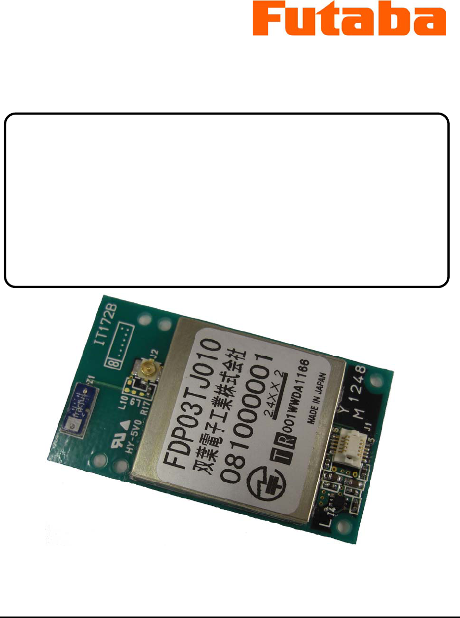
FDP03TJ010/020
2.4GHz Embedded Type Wireless Modem
Instruction Manual
Futaba Corporation
Industrial Radio Control

Ver.1.0
2
I Notice
This device complies with part 15 of the FCC rules. Operation is subject to the following
two conditions: (1) This device may not cause harmful interference, and (2) this device must
accept any interference received, including interference that may cause undesired operation.
This equipment has been tested and found to comply with the limits for a Class A digital
device, pursuant to part 15 of the FCC Rules. These limits are designed to provide
reasonable protection against harmful interference when the equipment is operated in a
commercial environment. This equipment generates, uses, and can radiate radio frequency
energy and, if not installed and used in accordance with the instruction manual, may cause
harmful interference to radio communications. Operation of this equipment in a residential
area is likely to cause harmful interference in which case the user will be required to correct
the interference at her/his own expense.
Any unauthorized changes or modifications to this device not expressly approved by Futaba
Corporation could void the user’s authority to operate the device and possibly result in
damage to the equipment and/or cause serious or fatal injuries to the operator or nearby
personnel.
This device is intended to be installed and used in accordance with the instructions contained
in this manual. Failure to comply with these instructions could void the user’s authority to
operate the device and possibly result in damage to the equipment and/or cause serious or
fatal injuries to the operator or nearby personnel.
II Important Safety Information
The list of dangers, warnings and cautions in this section contain important information that
will help ensure safe operation of the system. Please read carefully and understand all of
these items. All installers, operators and maintenance personnel should read and understand
this information before installation, use, or maintenance of the FDP03TJ010/020.
The FDP03TJ010/020 system by itself is not inherently dangerous. HOWEVER, WHEN
THE FDP03TJ010/020 IS CONNECTED TO OTHER EQUIPMENT FOR THE
PURPOSE OF CONTROL, SAFETY AND ALL POSSIBLE ASSOCIATED
DANGERS MUST ALWAYS BE GIVEN THE UTMOST CONSIDERATION
DURING SYSTEM INTEGRATION, DESIGN, INSTALLATION, AND USE.
The FDP03TJ010/020 may be used in virtually unlimited applications. Many of these
associated systems can, by themselves, pose a mechanical, electrical or other hazard to
operators and other persons or equipment. To address all possible applications and
associated safety hazards in this manual would be impossible. The warnings below and
throughout this manual give information that will allow safe installation and use the modem
system applications. If you have questions regarding the safety of your specific application,
please contact the appropriate people for help. Your Futaba sales representative,
representatives of the equipment being controlled, and the technical support staff at local
branch of Futaba Corporation are among those who can provide assistance with your safety
concerns.
The following warnings are included in the lists that follow but warrant repetition here:
In installations where the FDP03TJ010/020 is used to control motion or operation of
potentially dangerous equipment, it is imperative for safety that all operators and installers be
thoroughly trained in the normal function of that equipment before attempting to control it
remotely with the FDP03TJ010/020.

Ver.1.0
3
To help ensure safe operation of the equipment, the FDP03TJ010/020 must be connected so
that it will operate in a fail-safe way. In other words, the equipment being controlled
should stop or return to its safest state in the absence of a control signal or total loss of RF
transmission from the FDP03TJ010/020. Our system uses one of the most reliable methods
available to transmit data using radio signals. Many factors can affect a radio signal that
may block it or interfere enough to disrupt regular transmission. Because of this,
equipment motion or dangerous electrical current, for example, that continues during a
loss-of-signal condition could be very dangerous.
Ver.1.0
4
Four symbols are used in the margin of the following section and throughout the manual to
indicate the level of hazard or information listed.
The symbols are defined as follows:
Indicates a hazard that will cause severe personal injury, death, or
substantial property damage if the warning is ignored.
Indicates a hazard that can cause severe personal injury, death, or
substantial property damage if the warning is ignored.
Indicates a hazard that will or can cause minor personal injury, or
property damage if the warning is ignored.
Indicates installation, operation, or maintenance information that is
important but not hazard-related.
Please read the following safety information carefully. Some of these notices are
duplicated throughout the manual, in areas of associated content, for your benefit.
II.I General Safety Hazards and Notes
Improper installation and/or operation of the FDP03TJ010/020 can
cause serious or fatal injuries to the operator or nearby persons and
cause damage to the FDP03TJ010/020, and any equipment it is used to
control. Please read and understand this manual completely and the
manual of all equipment being controlled before attempting to operate
or install this system.
Always keep this manual at a location readily accessible to anyone
operating the system and related equipment. Ensure that all operators
have read and understood this manual, especially all safety and
operation procedures contained in it. Please refer to the section in this
manual titled How to Obtain Help for the contact that can supply
additional manuals or answers to questions not covered in this manual.
If this product is passed on to a different user, be sure that this manual
accompanies the product.
Be certain that the installer of this equipment reads and understands the
instruction manual of the equipment that is being connecting to before
attempting this installation.
The FDP03TJ010/020 should NOT be used in a manner in which
failure of the product or loss of the radio signal could cause damage to
the equipment being controlled, or to anything in the area in which
such equipment is located. All integrated control systems should be
designed for “fail-safe” operation so that a temporary or permanent loss
of signal will not endanger any person, critical process, or equipment
(refer to the beginning of the safety section for further explanation).
The system design should ensure that the equipment being controlled
will initial to its safest state in the event of signal loss.
The FDP03TJ010/020 contains no user serviceable parts. If the unit
requires service, contact your sales representative or local branch of
Ver.1.0
5
Futaba Corporation per instructions the section titled How To Obtain
Help. Do not disassemble or attempt to repair the FDP03TJ010/020
yourself. Doing so could void your warranty and may void the user’s
authority to operate the device.
Contact Futaba before using the FDP03TJ010/020 in safety critical
applications such as medical equipment, aircraft, hazardous materials
handling, etc.
II.II Installation Safety Hazards and Notes
Use only the proper regulated DC voltage supplied to the
FDP03TJ010/020. Use of any other voltage may permanently damage
the modem and/or cause the modem to malfunction and create a shock
or fire hazard.
Be certain that all AC power outlets used the power adapters have been
properly installed, grounded, and fused. An electrical shock hazard
may exist if this unit is powered by a faulty power outlet or source.
If such a situation is discovered, immediately discontinue use until the
power source and outlet have been properly installed, grounded, and
fused by an electrician or other authorized person.
Be sure to wire the power connections correctly. Incorrect wiring can
damage the system, cause it to malfunction and/or create a shock and
fire hazard.
Ensure that the FDP03TJ010/020 power and the power to the
equipment to be controlled are turned off before connecting or
disconnecting the cable between them. This will help prevent
accidental damage to the system and unexpected operation and/or
injury.
Be sure the FDP03TJ010 power, the power to the equipment that is
being connecting to it, and the DC power source are all turned off
before wiring and connecting the power cable.
Be sure that the supplied power is within the specified range.
Voltages outside the specified range may damage the
FDP03TJ010/020.
Be sure that the power source has sufficient current capacity.
Insufficient current may cause the unit to malfunction.
Securely attach the antenna cable to the FDP03TJ010/020 and
equipment/power source to which it is connected. Failure to do so
could cause an unexpected system failure.
Below comment should be written on a product label when the
FDP03TJ010/020 is embeded into any products.
“This device contains FCC ID:AZP-FDP03”
Ver.1.0
6
Antenna Installation Hazards and Notes
Be sure to keep all systems and antennas clear of power lines.
Permanent equipment damage and severe shock injury or death can
occur if the system contacts power lines.
Contact Futaba before connecting any antenna not provided by Futaba
specifically for the FDP03TJ010/020. Attaching any non-authorized
antenna may be in violation of FCC regulations.
Before each use, verify that the antenna (and antenna cable, if used) is
securely attached and in good condition. A loose antenna or cable
may severely reduce the operating range of the system.
The FDP03TJ010/020 operates at frequencies in the 2.4 GHz band.
These frequencies are more directional than lower frequencies and are
easily reflected. If there are metal structures nearby, the effective
range may be shortened or the directional properties may be further
narrowed. To help avoid this, mount the antenna as far away as
possible from surrounding metallic structures.
Multipath problems occur easily at frequencies in the 2.4 GHz band.
When multipath problems are present, moving the antenna around 10
cm may result in improved communication or, conversely, worsened or
complete loss of communication. Futaba recommends that the
mounting position of the antenna be determined after testing and
verifying optimal communication conditions.
When installing multiple FDP03TJ010/020 that will use different
frequency groups in the same area, FDP03TJ010/020’s antennas of
different frequency groups must be mounted at least 6 feet (2 meters)
apart. Failure to do so may severely reduce the modem operating range.
Please contact Futaba for information about antenna separation when
using the FDP03TJ010/020 and other wireless products in the same
area.
Ver.1.0
7
II.III Environmental Safety Hazards and Notes
If the FDP03TJ010/020 has been stored at a temperature beyond the
specified operating temperature range for the system, it may not
function properly. Allow it to return to normal temperatures before
use. Refer to APPENDIX A – TECHNICAL SPECIFICATIONS for the
actual operating temperature range.
The FDP03TJ010/020 is a precision electronic device with a rugged
design that is intended for industrial applications. However, do not
install it where it will encounter excessive vibrations. In some cases,
isolation mounts may be used to isolate the modem from the
equipment’s vibration. Excessive vibration can permanently damage
the modem and/or cause it to malfunction.
Do not operate the FDP03TJ010/020 in environments where it will be
subjected to excessive moisture (such as rain or water spray), dust, oil,
or other foreign matter (such as metal particles). Doing so may
permanently damage the modem and/or cause it to malfunction. If it
does become wet or contaminated, correct the situation, verify proper
operation and have any problems corrected before using it to control
other equipment. If necessary, the modem can be mounted inside a
protective or waterproof enclosure. If the enclosure is metallic, the
antenna must be mounted externally or the effective operating range
will be severely limited.
The FDP03TJ010/020 is designed for indoor use. When using it
outdoors, the modem should be mounted in a waterproof enclosure and
the ambient temperature range should be checked to insure that it is
within the modem’s specifications. Always use the modem within its
specified environmental ranges.
II.IV Other Notice
Italicized gothic word used in this manual shows functional and
technical term especially important for the FDP03TJ010/020.
Ver.1.0
8
Operational Safety Hazards and Notes
Before each use of the FDP03TJ010/020, ensure that the area where the
equipment will be operated is clear of people or obstacles that may
affect its safe operation.
Before each use of the FDP03TJ010/020, verify that both the
equipment being controlled and the modem are in proper operating
condition.
When rewriting the FDP03TJ010/020’s memory registers, do not turn
the modem’s power off. If the power is interrupted, the memory
contents may be lost or corrupted and the modem operation will be
unpredictable. If the memory contents are lost or corrupted, they may
be restored to original initial settings by reinitializing them.
Do not attempt to operate remotely controlled equipment outside the
communication range of the FDP03TJ010/020. Doing so could cause
loss of control of the equipment.
III System Identification
For future reference, please take a moment to fill in the information below. This information
will help us respond as quickly as possible should your FDP03TJ010/020 ever need repair or
replacement.
Model Name and Number: FDP03TJ010/020
Serial Number:
Date of Purchase:
Distributor Name:
Distributor Address:
Distributor Phone Number:

Ver.1.0
9
IV Limited Warranty
FUTABA WARRANTS ONLY THAT THE INDUSTRIAL RADIO CONTROL SYSTEM
GOODS OR PRODUCTS FURNISHED HEREWITH SHALL BE FREE FROM DEFECTS
IN MATERIAL AND WORKMANSHIP UNDER NORMAL CONDITIONS OF USE AND
SERVICE FOR A PERIOD OF ONE (1) YEAR FROM THE DATE OF SALE TO THE
PURCHASER WHO IS THE FIRST BUYER OF THE GOODS FOR USE OR
CONSUMPTION AND NOT FOR RESALE OTHER THAN AS A COMPONENT OF
ANOTHER PRODUCT MANUFACTURED FOR SALE BY SUCH PURCHASER
(“CONSUMER”). FUTABA’S LIABILITY, WHETHER BASED ON BREACH OF
WARRANTY OR NEGLIGENCE, SHALL BE LIMITED, AT FUTABA’S ELECTION, TO
REPLACEMENT OR REPAIR OF ANY SUCH NONCONFORMING GOODS, F.O.B.
FUTABA’S U.S.A. PLANT, OR, AT FUTABA’S ELECTION, CREDIT FOR THE NET
PURCHASE PRICE OF SUCH GOODS. ALL CLAIMS HEREUNDER MUST BE MADE
IN WRITING DURING THE WARRANTY PERIOD, AND FUTABA SHALL HAVE THE
RIGHT PRIOR TO ANY RETURN OF GOODS TO INSPECT ANY GOODS CLAIMED
TO BE NONCONFORMING, AND IN ANY EVENT RESERVES THE RIGHT TO
REJECT CLAIMS NOT COVERED BY WARRANTY. THIS LIMITED WARRANTY
CONSTITUTES FUTABA’S SOLE WARRANTY. FUTABA MAKES NO OTHER
WARRANTY OF ANY KIND, EXPRESS OR IMPLIED, AND EXPRESSLY
DISCLAIMS ANY IMPLIED WARRANTY OF MERCHANTABILITY OR FITNESS
FOR A PARTICULAR PURPOSE. FUTABA’S WARRANTY SHALL NOT APPLY IF,
AMONG OTHER LIMITATIONS CONTAINED HEREIN OR FURNISHED WITH THE
PRODUCT, BUYER, OR CONSUMER, OR ANY USER OF THE PRODUCT (A)
ALTERS SUCH PRODUCT, OR (B) REPLACES ANY PART OF SUCH PRODUCT WITH
ANY PART OR PARTS NOT FURNISHED BY FUTABA FOR THAT PURPOSE, OR IF,
AMONG SUCH OTHER LIMITATIONS, PRODUCT FAILS TO OPERATE PROPERLY
OR IS DAMAGED DUE TO ATTACHMENTS OR COMPONENTS THAT ARE NOT
FURNISHED BY FUTABA FOR USE WITH OR REPAIR OF THE PRODUCT UNLESS
SUCH USE IS AUTHORIZED IN WRITING IN ADVANCE BY FUTABA.
THIS LIMITED WARRANTY EXTENDS ONLY TO THE CONSUMER AND IS NOT
ASSIGNABLE OR TRANSFERABLE. This limited warranty shall not apply to fuses,
lamps, batteries, or other items that are expendable by nature, unless otherwise expressly
provided.
This limited warranty does not cover any defect or damage to any of the goods caused by or
attributable to force, accident, misuse, abuse, faulty installation, improper maintenance,
improper electrical current, failure to install or operate in accordance with Futaba’s written
instructions, repair or alteration by unauthorized persons, or leaking batteries. THE
GOODS ARE SENSITIVE ELECTRONIC DEVICES REQUIRING SPECIAL
HANDLING, AND THIS LIMITED WARRANTY DOES NOT APPLY TO
PRODUCTS NOT HANDLED IN ACCORDANCE WITH INSTRUCTIONS SET
FORTH IN THE MANUAL.
THIS LIMITED WARRANTY DOES NOT COVER INDUSTRIAL RADIO
CONTROL PRODUCTS PURCHASED OR USED OUTSIDE OF THE UNITED
STATES WITHOUT FUTABA’S PRIOR APPROVAL.

Ver.1.0
10
V Returns
Futaba’s authorization must be obtained prior to return of any item for warranty or other
repair or replacement or credit and will reflect Futaba’s warranty service procedure.
Consumer’s warranty rights are governed by the terms of Futaba’s Limited Warranty, as
above described. Products returned for warranty repair or replacement or credit must be
carefully and securely packed for return, preferably in the original carton or equivalent. The
Consumer must also include in the carton a legible copy of the bill of sale or invoice which
shows the date of sale and the original Buyer’s and Consumer’s names, and also a letter
which gives the Consumer’s return address and contact telephone number, the model and
serial numbers of the product(s) returned, and a brief explanation of the problem or claimed
defect. Any returned products that are replaced by Futaba shall become the property of
Futaba. If after inspection Futaba determines the defect is not covered by its limited
warranty, Futaba will notify Consumer of its determination and will not undertake any repairs
or product replacement until Consumer agrees to pay for all necessary parts and materials,
labor (to be charged at Futaba’s standard repair rate then in effect), and other expenses
including all shipping charges and insurance. Futaba reserves the right to retain possession
of any product returned by Consumer because of defects not covered by Futaba’s warranty
until Futaba receives Consumer’s agreement as above noted or, if Consumer wants the
product returned without repair or replacement, Consumer reimburses Futaba for all shipping
and handling charges incurred by Futaba. Issuance of credit for returned items shall be made
at Futaba’s unfettered discretion. Consumer will not be entitled to return defective goods for
cash refunds. Consumer must inspect goods immediately and no rejection or revocation of
acceptance shall be permitted more than ten (10) days after delivery to, or first use by,
Consumer of the goods, whichever occurs first.
VI Patents – Copyrights – Trademarks – Proprietary Rights
If this product was manufactured according to designs or processes specified by Consumer,
Consumer shall indemnify and save Futaba, its affiliates, officers, agents, and employees,
harmless from any expense, loss, attorneys’ fees, costs, damages, or liability which may be
incurred as a result of actual or alleged infringement of patent, copyright, or trademark rights.
Furnishing of these products does not convey a license, implied or otherwise, under any
patent, copyright, or trademark right in which Futaba has an interest, nor does it convey rights
to trade secrets or any other proprietary information of Futaba.
VII Limitation of Damages and Action
IN NO EVENT SHALL FUTABA BE LIABLE TO CONSUMER, OR ANY OTHER
PERSON FOR ANY INCIDENTAL, CONSEQUENTIAL, OR SPECIAL DAMAGES
RESULTING FROM THE USE OF OR INABILITY TO USE THIS PRODUCT,
WHETHER ARISING FROM BREACH OF WARRANTY OR NEGLIGENCE OF
FUTABA, OR OTHERWISE. Any action hereunder must be commenced within one (1)
year of accrual of cause of action or be barred and forever waived. No modification or
alteration of Futaba’s Limited Warranty or any other provision of this paragraph or the above
paragraphs shall result from Futaba’s acknowledgment of any purchase order, shipment of
goods, or other affirmative action by Futaba toward performance following receipt of any
purchase order, shipping order, or other form containing provisions, terms, or conditions in
addition to or in conflict or inconsistent with any such provisions.

Ver.1.0
11
Contents
1. Overview..................................................................................................................................................1
2. Operating Modes......................................................................................................................................1
2.1 Packet Transmission Mode.....................................................................................................................1
2.2 Headerless Packet Transmission Mode ..................................................................................................4
2.3 Serial-Output Data Format of Receiver Side at The Transmission Mode..............................................5
2.4 Broadcast Transmission Mode ...............................................................................................................6
3. Data Transfer............................................................................................................................................7
3.1. Data Transfer Mode..................................................................................................................................7
FDP03 has 2 kinds of data transfer mode. One is “Interchange” mode that is possible to exchange data
between other FDP series. Another is “Communication Distance Extend” mode. The initial setting is
“Interchange” mode.........................................................................................................................................7
The data transfer mode should be same setting among communication partners. If the mode is different
each other, it is impossible to communicate with............................................................................................7
3.2. Setting.......................................................................................................................................................7
3.2.1. Setting by the memory register .......................................................................................................7
The data transfer mode can be changed by the bit 5 of the REG10. The initial setting of the bit 5 is “0”.
It means that “Interchange” mode. For more detail, please check Section 8. ..............................................7
3.2.2. Setting by command........................................................................................................................7
The data transfer mode can also be changed by SPD command. For more detail, please check Section 9.3.
7
3.3. Difference of 2 modes ..............................................................................................................................7
Interchange Mode............................................................................................................................................7
It is possible to communicate between other FDP series such as FDP01 and FDP02.....................................7
Communication Distance Extend Mode..........................................................................................................7
Wireless communication distance is extended to twice as long as “Interchange” mode.................................7
4. Transmission Timing................................................................................................................................8
4.1 Transmission Timing..............................................................................................................................8
4.2 Time period of the case that data re-transmission of divided packet is occurred at packet transmission
mode....................................................................................................................................................12
5. Low Power Stand-by Mode....................................................................................................................13
This mode realizes low power consumption drive by switching ON and Off of RF circuit. It is possible to
set this low power stand-by mode by the memory register (REG21: bit 2) or the command. If this mode is
set by the command, this mode is released by the main power OFF or by set to power down mode. ..........13
5.1. Operation Flow ...................................................................................................................................13
5.2. Setting .................................................................................................................................................13
5.2.1. Setting by the memory register........................................................................................................13
5.2.2. Setting by the command ..................................................................................................................14
6. RF Circuit Power Control Mode ............................................................................................................15
6.1. Operation Flow ...................................................................................................................................15
8. Registers.................................................................................................................................................17
8.1. List of Registers ..................................................................................................................................17
8.2 Explanation of Registers ......................................................................................................................18
9. Frequency...............................................................................................................................................27
9.1 Frequency Range..................................................................................................................................27
9.2 Frequency Setting and Frequency Group.............................................................................................28
9.3 Commands............................................................................................................................................29
9.3.1 List of commands..............................................................................................................................29
9.3.2 Command input format .....................................................................................................................29
9.3.3 Explanation of commands.................................................................................................................30
10. Interface................................................................................................................................................47
10.1. Pin Layout .........................................................................................................................................47

Ver.1.0
12
10.2. Recommended Connector .................................................................................................................47
10.3. Electrical Characteristics...................................................................................................................48
10.4. AC Characteristics.............................................................................................................................48
10.4.2 Low Power Stand-by Mode.............................................................................................................49
10.5.3. RF Circuit Power Control Mode......................................................................................................50
10.5.4. Power Down Mode........................................................................................................................51
10.5.5. Parameter Initializing by /SHUT and /INI Terminal .......................................................................52
11.1. Outer Dimensions..............................................................................................................................53
11.2. Weight ...............................................................................................................................................53
11.3. Power Supply ....................................................................................................................................53
11.4. Radio Specifications..........................................................................................................................54
10.5 Interface..............................................................................................................................................54
10.6 Environment.......................................................................................................................................54
11. Notes.....................................................................................................................................................55
11.1 Data Communication Delay ...............................................................................................................55
11.1.1 Delay at the transmission side .........................................................................................................55
11.1.2 Delay at the reception side ..............................................................................................................55
11.2 Reception of Same Packets ................................................................................................................55
11.3 Timing of Command Input.................................................................................................................55
11.4 Headerless Packet Transmission Mode ..............................................................................................56
11.4.1 Input data.........................................................................................................................................56
11.4.2 Measures against packet loss...........................................................................................................56
11.5 Occurrence of Data Loss Even under Hardware Flow Control..........................................................56
11.6 Frequency Setting in Multi-System Environment..............................................................................56
11.7 Timing of Command Input.................................................................................................................56
11.8 INI and RST Commands ....................................................................................................................56
11.9 Power-Down Mode ............................................................................................................................56
Ver.1.0
1
1. Overview
The FDP03TJ010/020 (hereinafter referred to as the "FDP03") is a 2.4GHz-band wireless radio modem with a
compact and low power consumption design. FDP03TJ010 should be connected to an external antenna by an
antenna connector. FDP03TJ020 equips built-in antenna
Do NOT place FDP03TJ020 near any metal objects. Because
FDP03TJ020 uses built-in antenna, RF radio will be blocked and will
have unnecessary reflections if it is placed near metal objects.
Communication distance of FDP03TJ020 will be dramatically changed
by the surrounding environment.
.
2. Operating Modes
The FDP03 has the following three transmission modes:
- Packet transmission mode
- Headerless packet transmission mode
- Broadcast transmission mode
2.1 Packet Transmission Mode
The FDP03 supports two types of wireless addresses. One is unique address and the other is group address.
At packet transmission mode, data packets are transmitted to the unique address and/or group address through
the serial port. AT this mode, the packet format should be text or binary data.
(1) Configuration of text packet
Command header Command Destination
address Data (message) Delimiter
1 byte 3 bytes 3 bytes 0 to 130 bytes 2 bytes
@ TXT 000 to 255 User defined data <Cr><Lf>
(2) Configuration of binary data packet
Command header Command Destination
address
Number of
data bytes Data (message) Delimiter
1 byte 3 bytes 3 bytes 3 bytes 0 to 130 bytes 2 bytes
@ TBN 000 to 255 000 to 130 User-specified defined
data <Cr><Lf>
Processing of packet transmission and reception
When a packet is input to a sender FDP03 via the serial port, the sender FDP03 checks whether the packet is
valid.
Then, if the packet configuration is invalid or a time gap between bytes is more than 5 seconds, the sender
FDP03 distinguishes an occurrence of a packet error and ignores the packet. At that time, the sender FDL01
notifies the occurrence of the packet error if the functions of "Enabling response" and "Enabling N0 response"
in he REG13 are turned on.
If the functions of “Enabling response” and “Returning P1 and P0 responses” in the REG13 register are turned
on, the sender FDP03 replies a P1 response to the host when it receives a valid packet data. However, the
sender FDP03 does not return any response if the functions of the REG13 register is different setting. Then,
the sender FDP03 transmits the packet through wireless transmission to the destination address, receiver
FDP03.
At receiver FDP03 side, it output the packet data through the serial port if configurations of packet are valid.

Ver.1.0
2
At that time, the receiver FDP03 responds an acknowledgement “ACK” signal to the sender FDP03 for
notifying data packet receiving if "Enabling destination address check at reception" function of the REG18
register is turned on. On the other hand, when the function of "Disabling destination address check at
reception" in the REG18 register is turned on, the receiver FDP03 does not return ACK signal to the sender
FDP03 and also it receives all packet data regardless of the destination address of the packet.
Packet data transmission from the sender to the receiver is finished when the sender FDP03 receives ACK
signal. At that time, the sender FDP03 outputs P0 response if "Enabling response" functions of the REG13
register is turned on. When the sender FDP03 cannot receive ACK signal within the time-out limit, the
sender FDP03 transmits the same packet data to the destination receiver through the air if the re-try frequency
is registered. (The re-try frequency can be set by REG11 register
When the receiver FDP03 receives the same packet several times, it ignores from the second data downward.
Also, the receiver FDP03 sends ACK signal to the sender FDP03 if the function of "Enabling destination
address check at reception" of REG18 register is turned on.
If the sender FDP03 cannot receive ACK signal even it sent packet data defined times by the REG11 register,
it outputs N1 response to the host device via the serial port when "Enabling response" function of REG13
register is turned on. No response signal is sent if the function of "Disabling response" in REG13 is turned
on
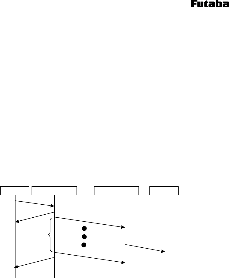
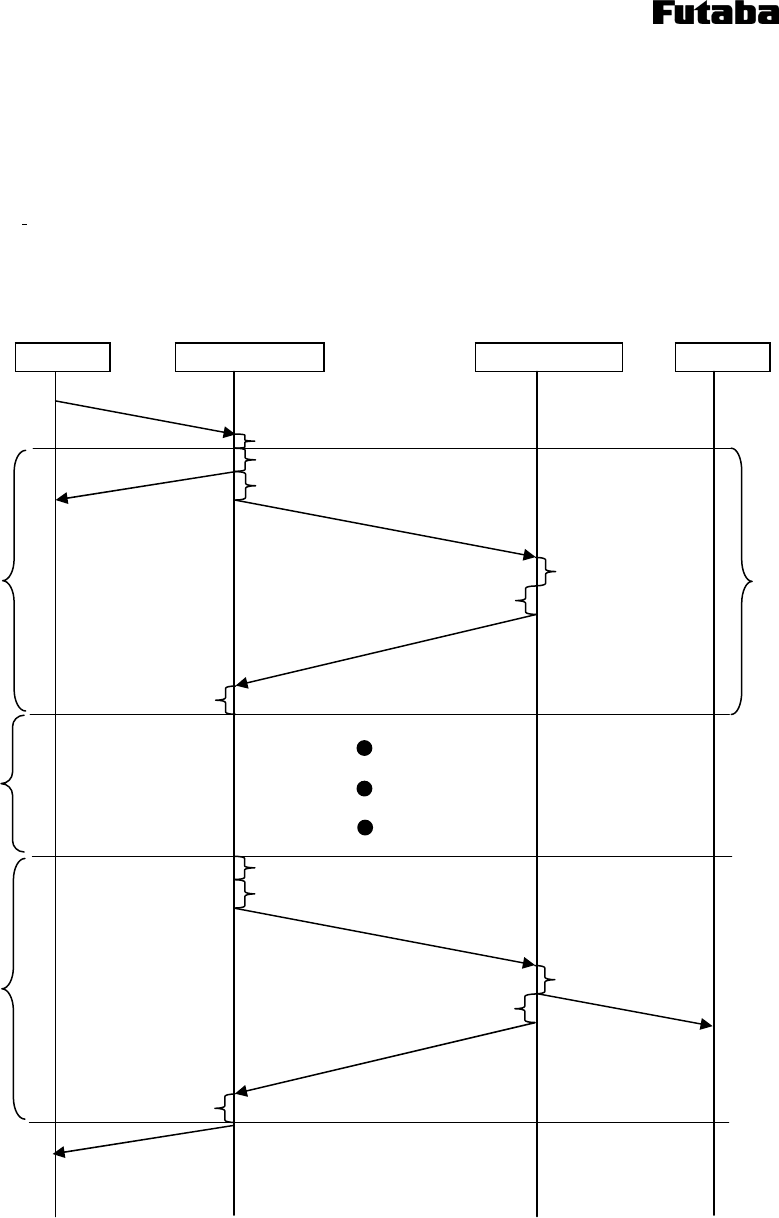
The figure below shows an operation example of data packet communication between a sender FDP03 that the
"Enabling response" and "Returning P0 and P1 responses" functions of REG13 register are turned on and a
receiver FDP03 that "Enabling destination address check at reception" function of REG18 register is turned on.
At the figure, data communication is completed by “ACK” signal retry.
① The Host 1 inputs data to the sender FDP03 via the serial port.
② The sender FDP03 recognizes the data packet configuration as valid and returns a P1 response to the Host
1 (Data is accepted).
③ The sender FDP03 transmits the data packet to the destination, which is the receiver FDP03, by wireless
transmission.
④ The receiver FDP03 receives the packet and outputs the received data packet to the Host 2 via the serial
port.
⑤ The receiver FDP03 returns ACK to the sender FDP03 by wireless transmission.
⑥ Time-out is occurred at the sender FDP03 because it cannot receive the receiver's ACK signal at the first
transmission. The sender FDP03 re-sends the data packet transmission.
⑦ The receiver FDP03 receives the same data packet as the previously received one. Thus, the receiver
FDP03 ignores the received data but returns ACK signal to the sender FDP03.
⑧ The sender FDP03 receives the ACK signal and outputs a P0 response to the Host 1.
Data input
P1 response
Wireless transmission
Return of ACK
Time-out Data output
P0 response
Host 1 FDP02 (sender) FDP02 (receiver) Host 2
①
②
③
⑤ ④
⑥
⑦
⑧
⑦
The data same as previously
received data is received and
discarded.
Return of ACK
Wireless transmission

Ver.1.0
3
After entering a command to the sender FDP03, do not input the next command
until the P0 response for the entered command is returned. Sending a new
command before the P0 response is received, it may cause of command error
and/or unpredictable operation.
When "Disabling response" function of REG13 register of the sender FDP03 is
turned on, the next command should be input after waiting a time period of
expected P0 response.

Ver.1.0
4
2.2 Headerless Packet Transmission Mode
By setting "Headerless packet transmission mode" on the REG03 register of the FDP03, the FDP03 transmits
packets by wireless transmission to a destination address that is defined by the REG02 register. At this mode,
a header part (command header "@", command "TXT" or "TBN", destination address, and number of message
bytes [for TBN command]) can be eliminated. The trigger of data transmission can be defined by the setting
of REG24 register. It can be selectable entering of "<Cr><Lf>" (0DH, 0AH) (i.e., carriage return and line
feed codes) or time over of the timeout period (a time gap limit between two data bytes that is set in the
REG26 register). Data transmission is triggered also when the number of message bytes exceeds 26 bytes.
It is also enable to set "Enabling response" and "Disabling response" mode in by the REG13 register at the
headerless packet transmission mode. Additionally, "Returning P1 and P0 responses" and "Returning P0
response" function can be selected when "Enabling response" mode is chosen. Moreover, "Enabling
destination address check at reception" and "Disabling destination address check at reception" function can be
selected by the REG18 register. For more details, see section 2.1 “Packet transmission mode”.
Also, it is selectable whether "<Cr><Lf>" (0DH, 0AH) is added on the received data by the settings of the bit
4 of the REG23 register.
In headerless packet transmission mode, maximum data buffer size for sending
data is 150 bytes and data transmission is started when message data size exceeds
26 bytes. When many message data are input consequently, the message buffer
may be overflowed and the message data may be lost. At that situation, the
hardware flow control function should be set. If "Enabling response" function
is selected in REG13 register, it is possible to judge whether data transmission is
succeeded or not. Thus it is recommended to set "Enabling response" function
even in headerless packet mode.
Additionally, the massage data may be lacked when the size is over 26 bytes.
To prevent for such an event, check each response on the sender and create
messages so that the loss of packets can be detected on the receiver FDP03.
The serial communication speed of all FDP03 should be same setting. If
different serial communication speeds are set between on the sender and the
receiver FDP03, data loss may occur on the slower speed side.

Ver.1.0
5
2.3 Serial-Output Data Format of Receiver Side at The Transmission Mode
Data format of the receiver side that outputs to the serial port varies depending on the transmission mode
(packet transmission or headerless packet transmission mode). The below table shows combination of the
data format and the mode setting.
Sender FDP03 (radio address is 000) Receiver FDP03 (radio address is 001)
Transmission mode Packet format Transmission mode Serial-output data format
Packet transmission (text
format) @TXT001HELLO<Cr><Lf> Packet transmission RXT000HELLO<Cr><Lf>
Packet transmission
(binary format)
@TBN001005HELLO<Cr>
<Lf>
Packet transmission RBN000005HELLO<Cr><Lf>
Packet transmission (text
format) @TXT001HELLO<Cr><Lf> Headerless* HELLO
Packet transmission
(binary format)
@TBN001005HELLO<Cr>
<Lf>
Headerless* HELLO
Headerless packet
transmission + <Cr><Lf> HELLO<Cr><Lf> Packet transmission RBN000007HELLO<Cr><Lf>
<Cr><Lf>
Headerless packet
transmission + time-out HELLO Packet transmission RBN000005HELLO<Cr><Lf>
Headerless packet
transmission + <Cr><Lf> HELLO<Cr><Lf> Headerless* HELLO<Cr><Lf>
Headerless packet
transmission + time-out HELLO Headerless* HELLO
* If "Adding '<Cr><Lf>' to received data" function of the receiver FDP03 is turned on by the bit 4 of REG23
(setting value is 1) at the headerless transmission mode, "<Cr><Lf>" is added at the end of the data that is
output to serial port.
Ver.1.0
6
2.4 Broadcast Transmission Mode
It is possible to send data by broadcast transmission. Broadcast transmission mode can be used by setting the
destination address to “255” at packet transmission or headerless packet.
In broadcast transmission mode, the sender FDP03 transmits data packet defined times by REG11 register + 1
time. If "Enabling response" function is turned on, the sender FDP03 sends response signal to the host. For
more details, see the section 2.1.
At broadcast transmission mode, the receiver FDP03 does not return ACK signal regardless of the REG18
register setting. Also, when the receiver FDP03 receives redundant data packet, it ignores duplicated
packets .
The below figure shows the data flow of broadcast transmission mode that "Enabling response" and
"Returning P0 and P1 responses" functions of the sender FDP03 is turned on.
① Host 1 inputs broadcast data to the sender FDP03.
② The sender FDP03 recognized the data packet configuration is valid and returns a P1 response to the host 1
(data is accepted).
③ The sender FDP03 broadcasts data packet defined times by REG11 register + 1 by air .
④ When the receiver FDP03 receives the packet correctly, it outputs the received data packet to the host 2 via
the serial port.
⑤ When the sender FDP03 completes all data transmission, it outputs a P0 response to the host 1.
Input of data with
destination address
set to "255" Wireless transmission
"Retransmission
count' + 1" times
Data output
Host 1 FDP02 (sender) FDP02 (receiver) Host 2
P1 response
①
②
③
④
⑤ ③
Wireless transmission
P0 response

Ver.1.0
7
3. Data Transfer
3.1. Data Transfer Mode
FDP03 has 2 kinds of data transfer mode. One is “Interchange” mode that is
possible to exchange data between other FDP series. Another is “Communication
Distance Extend” mode. The initial setting is “Interchange” mode.
The data transfer mode should be same setting among
communication partners. If the mode is different each other,
it is impossible to communicate with.
3.2. Setting
3.2.1. Setting by the memory register
The data transfer mode can be changed by the bit 5 of the REG10. The initial
setting of the bit 5 is “0”. It means that “Interchange” mode. For more detail, please
check Section 8.
3.2.2. Setting by command
The data transfer mode can also be changed by SPD command. For more detail,
please check Section 9.3.
3.3. Difference of 2 modes
Interchange Mode It is possible to communicate between
other FDP series such as FDP01 and
FDP02.
Communication Distance
Extend Mode Wireless communication distance is
extended to twice as long as
“Interchange” mode.
Ver.1.0
8
4. Transmission Timing
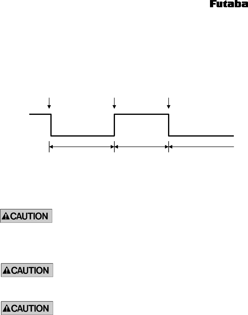
4.1 Transmission Timing
At packet transmission mode, the FDP03 can transmit up to 130 bytes of message as a single packet.
However, the radio transmission unit of the data is divided by 26 bytes. Since the FDP03 internally divides a
message by 26 bytes when the packet size is bigger than 26 bytes, total data transmission time is varies with
the data size. .
In headerless packet transmission mode, the FDP03 transmits each message in units of 26 bytes without
dividing them.
The time required for communication is shown below.
①@TXT*** input
Host 1 FDP02 (Sender) FDP02 (Receiver) Host 2
④P1 response output
⑫P0 response output
⑦Reception
p
rocessing: 1.2 ms
⑥Message transmission: 0.45 ms
⑩ACK reception
p
rocessing: 0.7 ms
⑨ACK transmission: 0.45 ms
⑧ACK packet generation: 0.7 ms
⑪RXT*** output
②Command processing: 1 ms
③Packet generation (first time): 0.7 ms
⑤Carrier sensing: 0.1 ms
First message
transmission 4.3 ms
Data input
③Packet generation (fifth time): 0.7 ms
⑤Carrier sensing: 0.1 ms
⑩ACK reception
p
rocessing: 0.7 ms
Fifth message
transmission
Second to fourth
message
transmission
⑦Reception
p
rocessing: 1.2 ms
⑥Message transmission: 0.45 ms
⑨ACK transmission: 0.45 ms
⑧ACK packet generation: 0.7 ms

Ver.1.0
9
① Serial input of transmission data packet
The time required to data input between the host1 and the sender FDP03 is defined by below
communication parameter.
- Line speed (9,600 to 115,200 bps)
- Data bit length (7 or 8 bits)
- Parity bit (odd, even, or no parity)
- Stop bit length (1 or 2 bits)
- Start bit length (always 1 bit)
For example, data transmission time is 87us when the line speed is 115,200bps, the data bit length is 8 bits,
the parity bit is NONE, the stop bit length is 1 and the start bit length is 1. (Time of data transmission for
1 bit is 8.7us and 1byte is 10bits.)
If the transmission is text data at the packet transmission mode, size of send data packet is message bytes +
9 bytes because the header is 7 bytes and delimiter is 2 bytes.
If the transmission is binary data at the packet transmission mode, size of send data packet is message
bytes + 12 bytes because the header is 10 bytes and delimiter is 2 bytes.
At the headerless packet mode, the data size is message bytes + 2 bytes if delimiter is included. On the
other hand, if the trigger of transmission is “time-out”, the data size is the same as the message size.
However, the data transmission time is defined by “time-out” setting by REG24 and REG26 register.
② Command processing
It is the time for internal processing to of receiving and decoding the packet that comes from the serial port.
It takes 1.5 ms.
③ Transmission packet generation
It is the time for transmission data packet generation. It takes 1.0 ms.
④ Response of input data format acceptance
It is the time for response when the receiving data format is valid. The length is 4 bytes. It depends on
the parameters of ①.
⑤ Carrier sensing
It is the time for detection whether other radio station uses same frequency band. If other radio station
uses the frequency band, the sender FDP03 does not transmits the data. It takes 0.1 ms.
If the wireless environment is very severe, noise level is very high and/or other
wireless systems occupy the area, the sender FDP03 may be not able to transmit
any data because of carrier sensing.
⑥ Message transmission
It is the time for data transmission and it takes 0.45 ms.
⑦ Data reception processing
It is the time for the receiving data processing and it takes 2.4 ms.

Ver.1.0
10
⑧ ACK packet generation
It is time for ACK packet generation. It takes 1.0 ms
⑨ ACK packet transmission
It is time for ACK packet transmission that the acknowledgement of data packet reception. It takes 0.45
ms.
⑩ ACK reception processing
It is processing time for ACK packet. It takes 1.0ms.
⑪ Serial output of received packet
It is time for output of received data packet to the host 2 through the serial port. The time period depends
on the communication setting between the host 2 and the receiver FDP03.
If the transmission is text data at the packet transmission mode, size of output data packet is message bytes
+ 8 bytes because the header is 6 bytes and delimiter is 2 bytes. If the transmission is binary data at the
packet transmission mode, size of send data packet is message bytes + 11 bytes because the header is 9
bytes and delimiter is 2 bytes.
At the headerless packet mode, the data size is message bytes + 2 bytes if delimiter is included. On the
other hand, if the trigger of transmission is “time-out”, the data size is the same as the message size. If
"Adding '<Cr><Lf>' to received data" function of the receiver FDP03 is turned on by the bit 4 of REG23
(setting value is 1) at the headerless transmission mode, "<Cr><Lf>" is added at the end of the data and it
consume 2 bytes.
⑫ Indication of data transmit completion
A response is returned to the host 1when the data transmission is completed correctly. The length of
response data is 4 bytes, and the time period of response return depends on the parameter settings of the
communication parameters that are described in above section ①.
Based on the above data processing flow, the total time for the data packet transmission from the host 1 to the
host 2 can be calculated like below. (In the below calculation, no data packet re-transmission is supposed.)
× 1000 × (size of message in bytes + A) + B + 6.4 × (C – 1)
+ × 1000 × (size of message in bytes + D) + 5.5 [ms] Expression 1
A: Text data is transmitted at packet transmission mode: 9
Binary data is transmitted at packet transmission mode: 12
Trigger of the data transmission is delimiter at headerless packet transmission mode: 2
Trigger of the data transmission is time-out at headerless packet transmission mode: 0
B: Trigger of the data transmission is time-out at headerless packet transmission mode:
"Value of REG26" x 10 [If the bit 0 of REG24 is “1”]
"Value of REG26" x 1 [If the bit 0 of REG24 is “0”] (*1)
Others: 0
C: Data size of message is 0 to 26 bytes: 1 (*2)
Data size of message is 27 to 52 bytes: 2
Data size of message is 53 to 78 bytes: 3
Data size of message is 79 to 104 bytes: 4
Data size of message is 105 to 103 bytes: 5
D: Text data is transmitted in packet transmission mode: 8
Binary data is transmitted in packet transmission mode: 11
Bit length per byte
Line speed of the sender
Bit length per byte
Line speed of the receiver

Ver.1.0
11
Trigger of the data transmission is delimiter at headerless packet transmission mode: 2
Trigger of the data transmission is time-out at headerless packet transmission mode 0
*1 If the setting value is less than 3ms, the value of “B” will be “3”.
*2 At headerless packet mode, the value of C is always 1.
The total time until completion of the data transmission is calculated by below formula.
× 1000 × (size of message in bytes + A + 4) + B + 6.4 × C + 1.5 Expression 2
A: Text data is transmitted at packet transmission mode: 9
Binary data is transmitted at packet transmission mode: 12
Trigger of the data transmission is delimiter at headerless packet transmission mode: 2
Trigger of the data transmission is time-out at headerless packet transmission mode: 0
B: Trigger of the data transmission is time-out at headerless packet transmission mode:
"Value of REG26" x 10 [If the bit 0 of REG24 is “1”]
"Value of REG26" x 1 [If the bit 0 of REG24 is “0”] (*1)
Others: 0
C: Data size of message is 0 to 26 bytes: 1 (*2)
Data size of message is 27 to 52 bytes: 2
Data size of message is 53 to 78 bytes: 3
Data size of message is 79 to 104 bytes: 4
Data size of message is 105 to 103 bytes: 5
*1 If the setting value is less than 3ms, the value of “B” will be “3”.
*2 At headerless packet mode, the value of C is always 1.
Bit length per byte
Line speed of the sender
Ver.1.0
12
4.2 Time period of the case that data re-transmission of divided packet is occurred at packet
transmission mode
When packet data size is exceeding 26 bytes, it is divided into several packets that data size is 26 bytes. At
that time, each divided packet is sent defined re-transmission times. Thus, maximum data transmission
period will be (setting of REG11 register + 1) x 5 times. (REG11 register is a parameter of data
re-transmission frequency.)
It takes 7.6 ms if data transmission failure is occurred once. Therefore, total data processing time is like
below formula.
× 1000 × (size of message in bytes + A + 4) + B + 7.6
× frequency of data transmission Expression 3
A: Text data is transmitted at packet transmission mode: 9
Binary data is transmitted at packet transmission mode: 12
Trigger of the data transmission is delimiter at headerless packet transmission mode: 2
Trigger of the data transmission is time-out at headerless packet transmission mode: 0
B: Trigger of the data transmission is time-out at headerless packet transmission mode:
"Value of REG26" x 10 [If the bit 0 of REG24 is “1”]
"Value of REG26" x 1 [If the bit 0 of REG24 is “0”] (*)
Others: 0
* If the setting value is less than 3ms, the value of “B” will be “3”.
In this case, if data transmission failure is occurred in any given
divided packet, following packets are not transmitted. Therefore,
total data transmission period is fluctuated.
Example 1: At the line speed set to 115,200 bps and bit length per byte set to 10 bits, time period of the data
transmission failure detection is 53.1 ms if the first packet data is fail to transmit. (Size of the
message is 130 bytes. Setting of data re-transmission frequency is 10 times.)
(10/115,200) × 1,000 × (130 + 9 + 4) + 7.6 × (10+1) × 1 = 96.0 [ms]
Example 2: At the line speed set to 115,200 bps and bit length per byte set to 10 bits, time period of the data
transmission failure detection is 215.9 ms if the fifth packet data is fail to transmit. (Size of the
message is 130 bytes. Setting of data re-transmission frequency is 10 times.)
(10/115,200) × 1,000 × (130 + 9 + 4) + 7.6 × (10 + 1) × 5 = 430.4 [ms]
As shown above, the total transmission time is largely fluctuated by the condition of the data transmission.
To keep communication response well, size of the message should be less than 26 bytes.
Bit length per byte
Line speed of the sender
Ver.1.0
13
5. Low Power Stand-by Mode
This mode realizes low power consumption drive by switching ON and Off of RF circuit. It is possible to set
this low power stand-by mode by the memory register (REG21: bit 2) or the command. If this mode is set by
the command, this mode is released by the main power OFF or by set to power down mode.
5.1. Operation Flow
By repeating “stand-by mode” and “sleep mode”, the power consumption at the RF circuit is reduced. Duration
of the “stand-by mode” and “sleep mode” can be set by REG22, bit 1 of REG24 and REG25.
If the FDP03 receives data that destination address is matched and REG18 (address check) is set to “Enabling
destination address check at reception”, the duration of the “stand-by mode” is extended. The extended time
duration is set by REG21 or command setting. When the FDP03 cannot receive next data packet during the
extended stand-by time, it becomes “sleep mode”.
If the data packet is sent by broadcasting mode and/or the REG18
setting is “Disabling group address check at reception”, the FDP03 does not
turn to the “Extended Stand-by mode” even if the extended time duration is set
by REG21.
5.2. Setting
5.2.1. Setting by the memory register
It is possible to set “Low Power Stand-by Mode” by bit 2 of REG21. At that time, time duration of “Stand-by”
is set by REG22, that of “Sleep” is set by bit 1 of REG24 and REG25 and that of “Extended Stand-by Time” is
set by bit 4 to 7 of REG21. For more detail, please check “Registers” section below.
Current Consumption
Stand-By Sleep
Current Consumption
Stand-By Sleep
FDP02 receives data packet
Extended Stand-by Time

Ver.1.0
14
5.2.2. Setting by the command
It is also possible to set “Low Power Stand-by Mode” by below listed commands. For mode detail, please
check “Commands” section below.
Command Function
POF Turn off the Low Power Stand-by Mode
PON Turn on the Low Power Stand-by Mode
PTE Show/Set Extended Stand-by mode time duration
PTN Show/Set time duration of Stand-by mode
PTS Show/Set time duration of Sleep mode
Ver.1.0
15
6. RF Circuit Power Control Mode
This mode can realize low power consumption operation by stopping RF circuit.
6.1. Operation Flow
It is possible to control ON/OFF of RF circuit by ROF/RON command. For more detail of ROF/RON
command, please check “Commands” section below.
Wireless communication is completely cut when RF circuit is OFF. Therefore,
RON command should be executed to turn ON the RF circuit if wireless
communication is returned.
If the FDP03 is re-booted and/or the operation mode is returned from “Power
Down” mode, the RF circuit will be turned ON. Thus, it is necessary to execute
ROF command to cut the RF circuit again.
Current Consumption
RF OFF RF ON RF OFF
ROF Command ROF CommandRON Command
Ver.1.0
16
7. Power Down Mode
If the voltage level of the /SHUT terminal is set to “Low” level, the power source of the FDP03 is cut and it
becomes to “Power Down Mode”. During the “power Down Mode”, all functions of FDP03 does not work.
When the voltage level of the /SHUT terminal is set to “High” level, the FRP02 is to be the operation mode.
Do NOT set “Power Down Mode” during the FDP03 is accessing the
memory registers. If the voltage level of the /SHUT terminal is
turned to “Low” level, the settings of the memory registers are
vanished. Therefore, do NOT touch the /SHUT terminal during REG
commands are running.
The parameters that are set by REG commands are cleared when the
operation mode is changed from the “Power Down Mode” to “Normal
Operation Mode”. Thus, the parameters should be set by the memory
registers.
Do NOT input any data to the signal line during the Power Down
mode. The FDP03 will get damage if data are input during the Power
Down mode. Also, do NOT input high impedance signal to the
terminals of the host to avoid unnecessary data output.
Current Consumption
Power Down Mode Normal Operation Mode Power Down Mode
/SHUT = “Low” /SHUT = “Low” /SHUT = “High”

Ver.1.0
17
8. Registers
All settings of the FDP03 are stored in its registers.
8.1. List of Registers
Below table shows list of all registers.
Register Function Default Setting range Remarks
REG00 Local station address 00H 00H to EFH 000 to 239
REG01 Group address F0H F0H to FEH 240 to 254
REG02 Destination address of
Headerless-packet 00H 00H to FFH 000 to 255 (to be used for headerless packet
transmission)
REG03 Transmission mode F0H F0H, FFH Default: Packet transmission mode
REG04 ID code 1 00H 00H to FFH
REG05 ID code 2 00H 00H to FFH
REG06 Frequency group 03H 01H to 03H Default: 3-band mode
REG07 Frequency 1 02H 02H to 4DH Default: 2,402 MHz
REG08 Frequency 2 2AH 02H to 4DH Default: 2,442 MHz
REG09 Frequency 3 4DH 02H to 4DH Default: 2,477 MHz
REG10 Data transfer 01H 01H, 21H Default: Interchange mode
REG11 Retransmission frequency 0AH 00H to FFH Default: 10 times
REG12 Unused 00H -
REG13
Serial response of sent data
00H 00H to 07H
Default: "Returning P0 and P1 responses,"
"Enabling N0 response," and "Enabling
response"
REG14 Unused 00H -
REG15 Command recognition interval 00H 00H to FFH Default: 0 ms (to be used for headerless
packet transmission)
REG16 Unused 00H -
REG17 Buffer clear 64H 01H to FFH Default: 10s
REG18 Address check 8DH 8CH, 8DH
Default: "Enabling destination address
check at reception"
REG19 Unused 00H -
REG20 Wired-communication setting 1
(serial communication) 00H 00H to FFH Default: 9,600 bps, 8 data bits, no parity,
and 1 stop bit
REG21
Wired-communication setting 2
(flow control),
Low power stand-by mode,
Extended stand-by time
09H 00H to FFH
Default: "Disabling hardware flow control"
Without low power stand-by mode
Extended stand-by time is Zero
REG22 Low power stand-by time 04H 01H to FFH- Default: 40ms
REG23
Wired-communication setting 3
00H 00H,10H
Default: "Not adding '<Cr><Lf>' to received
data" (to be used for headerless packet
transmission)
REG24
Delimiter for headerless-packet
transmission
Unit of sleep time duration
C1H 80Hto 83H
C0H to C4H
Default: <Cr><Lf> (to be used for
headerless packet transmission)
x 10ms
REG25 Sleep time 04H 01H to FFH Default: 40ms
REG26 Time-out of headerless-packet
data input 01H 01H to FFH Default: 10 ms (to be used for headerless
packet transmission)
* To initialize the registers, use the INI command (see Section 8.3.3) or input an initialization signal from the
/INI pin (see Section 9.1).

Ver.1.0
18
8.2 Explanation of Registers
REG00 (local station address) [Default: 00H]
This register can set own wireless address. When the FDP03 receives a packet that destination is this
address, the FDP03 processes the packet. The setting range is 00H to EFH (000 to 239). If the value is
set to invalid range, the FDP03 returns N0 response.
REG01 (group address) [Default: F0H]
This is the wireless group address of the FDP03. When the FDP03 receives a packet that group is this
address, the FDP03 processes the packet.
If "Enabling destination address check at reception" function of the REG18 is turned on, the FDP03 returns
ACK signal to sender FDP03 when it receives a packet. Therefore, if "Enabling destination address check
at reception" function of all FDP03 in the system is turned on, all FDP03 that receive a packet return ACK
signal. Thus, to avoid unnecessary communication, the REG18 may be set to "Disabling destination
address check at reception".
The range of the setting value is F0H to FEH (240 to 254). If the value is set to invalid range, the FDP03
returns N0 response.
REG02 (headerless-packet destination address) (only for the headerless packet transmission mode)
[Default: 00H]
This register indicates the destination address of packet data in headerless packet transmission mode. This
register also indicates the wireless address of the connection destination when TS2 command is used.
The range of the setting value is 00H to FFH (000 to 255). If the value is set to invalid range, the FDP03
returns N0 response.
REG03 (transmission mode) [Default: F0H]
This register setting can change the transmission mode, which is packet transmission mode or headerless
packet transmission mode.
F0H Packet transmission mode (default)
FFH Headerless packet transmission mode
The value of the setting is F0H (packet transmission mode) or FFH (headerless packet transmission mode).
If the value is set to invalid range, the FDP03 returns N0 response.
REG04 (ID code 1) [Default: 00H]
This register setting defines data scramble ID. Combined with ID code 2 (REG05), variation of data
scramble ID is up to 65,536.
Range of the setting value is 00H to FFH and FDP03 returns N0 response if the value is out of the range.
The same scramble code (REG04 and REG05) must be set on all the
FDP03s in the system. If the scramble codes are different each other,
each FDP03 cannot communicate with.
Ver.1.0
19
REG05 (ID code 2) [Default: 00H]
This register setting defines data scramble ID. Combined with ID code 1 (REG04), variation of data
scramble ID is up to 65,536.
Range of the setting value is 00H to FFH and FDP03 returns N0 response if the value is out of the range.
The same scramble code (REG04 and REG05) must be set on all the
FDP03s in the system. If the scramble codes are different each other,
each FDP03 cannot communicate with.
REG06 (frequency group) [Default: 03H]
This register defines the number of frequencies to be used.
01H Use only the frequency set by REG07
02H Use the frequencies set by REG07 and REG08
03H Use the frequencies set by REG07 to REG09 (default)
The range of settings is 01H to 03H.
When the register is set to 01H, only a frequency that is set by REG07 is used.
When the register is set to 02H, two frequencies that are set by REG07 and REG08 are used as a frequency
group.
When the register is set to 03H, three frequencies that are set by REG07 to REG09 are used as a frequency
group.
FDP03 returns N0 response if the value is out of the range.
The setting value of REG07, REG08 and REG09 should not be
duplicated when the setting of REG06 is “02H” and “03H”. If the
frequencies have duplication, the transmission frequency will not be
switched.
REG07 (frequency 1) [Default: 02H]
This register defines the frequency channel to be used for radio communication. The frequency channel
that is set by this register is always used.
The range of the setting is 2,402 MHz to 2,477 MHz. It is possible to set it by both 2-digital hexadecimal
value (02H to 4DH) and 3-digit decimal value (002 to 077). For more details of correspondence between
setting values and frequency channels, please refer section 5.1. FDP03 returns N0 response if the value is
out of the range.
REG08 (frequency 2) [Default: 2AH]
This register defines the frequency channel to be used for radio communication. The frequency channel
that is set by this register is applied when the RGE06 setting is 02H or 03H.
The range of the setting is 2,402 MHz to 2477 MHz. It is possible to set it by both 2-digital hexadecimal
value (02H to 4DH) and 3-digit decimal value (002 to 077). For more details of correspondence between
setting values and frequency channels, please refer section 5.1. FDP03 returns N0 response if the value is
out of the range.
Ver.1.0
20
REG09 (frequency 3) [Default: 4DH]
This register defines the frequency channel to be used for radio communication. The frequency channel
that is set by this register is applied only if the RGE06 setting is 03H.
The range of the setting is 2,402 MHz to 2477 MHz. It is possible to set it by both 2-digital hexadecimal
value (02H to 4DH) and 3-digit decimal value (002 to 077). For more details of correspondence between
setting values and frequency channels, please refer section 5.1. FDP03 returns N0 response if the value is
out of the range.
REG10 (Data Transfer) [Default: 01H]
Bit 7 and 6: Not used
Bit 5: Data transfer mode
0 Interchange mode (default)
1 Communication Distance Extend mode
The data transfer mode should be same setting among communication
partners. If the mode is different each other, it is impossible to
communicate with.
Bit 4 to 0: Not used
REG11 (retransmission count) [Default: 0AH]
This register defines the maximum frequency of data packet retransmission.
When the sender FDP03 cannot receive ACK signal from the receiver FDP03, it retransmits the data packet
"'defined value of this register' +1" times.
At broadcast transmission mode, the sender FDP03 always sends the data packet "'defined value of this
register' +1" times.
The enable setting range of this register is 00H to FFH (0 to 255 times). FDP03 returns N0 response if the
value is out of the range.
REG12 (unused) [Default: 00H]
This register is not used. It should be default setting “00H”.
Ver.1.0
21
REG13 (Serial response to packet input) [Default: 00H]
This register defines the responses for in-coming data packet from the host through the serial port.
Bits 7 to 3: Not used
Bit 2: N0 response
0 Enabling N0 response (default)
1 Disabling N0 response
Bit 2 is available only if the bit 0 is set to "Enabling response."
If this bit is set to “0” (Enabling N0 response), the FDP03 sends N0 response to the host thorough the serial port
when the packet data format from the host is invalid or time gap between bytes is more than 5 seconds.
If this bit is set to “1”, the FDP03 does not send any N0 response to the host
.
When the bit2 of REG13 is set to “1”, the FDP03 does not send any
response even if the packet format is invalid.
Bit 1: Normal response
0 Returning P0 and P1 responses (default)
1 Returning P0 response
Bit 1 is available only if the bit 0 is set to "Enabling response." By this setting, it is possible to select type
of response when the data packet configuration is valid.
If the bit 1 is set to “0”, the FDP03 sends P1 response to the host through the serial port when it receives a
data packet. Also, it sends P0 response to the host when the data transmission to the receiver is success.
When the data transmission to the receiver is failed, the FDP03 sends N1 response to the host.
If the bit 1 is set to “1”, the FDP03 sends P0 response to the host through the serial port when the data
transmission to the receiver is success and sends N1 response when the data transmission to the receiver is
failed.
Bit 0: Enabling response
0 Enabling response (default)
1 Disabling response
The bit 0 is defines whether the FDP03 send a response to the host or not.
When bit 0 is set to 0, the FDP03 sends particular specified responses to the host through the serial port.
When bit 0 is set to 1, the FDP03 does not send any response to the host.
When the 0 is set to “1”, the FDP03 does not send any
response even if the packet configuration is invalid.
During the register setting, the FDP03 always sends the
responses if it is any settings.

Ver.1.0
22
REG14 (unused) [Default: 00H]
This register is not used. It should be default setting “00H”.
REG15 (command recognition interval) (only for the headerless packet transmission mode) [Default: 00H]
If the packet to be transmitted in headerless packet transmission mode includes code "40H", which indicates
the command header (@), the data following the code is handled as a command, and the packet cannot be
transmitted normally. This register is used to avoid such problems. Code "40H" is handled as the
command header only when the code is input after a time gap between bytes that exceeds the value set in
this register.
The range of settings is 00H to FFH. The value is in units of 100 ms.
With the default setting (00H) of this register, code "40H" is always handled as the command header.
REG16 (unused) [Default: 00H]
This register is not used. It should be default setting “00H”.
REG17 (unused) [Default: 64H]
This register is not used. It should be default setting “00H”
REG18 (address check) [Default: 8FH]
Bits 7 to 2: Not used
Bit 1: Group address check
0 Disabling group address check at reception
1 Enabling group address check at reception (default)
Only if the bit 0 of REG18 is 0, the bit 1 is available.
When the bit 1 is set to “0”, the FDP03 receives all data packets whatever the destination address of the data
packet is. On the other hand, the FDP03 only receives the data packets that destination address is
consistent.
The FDP03 does not return ACK signal to the senders at both settings.
Bit 0: Destination address check
0 Disabling destination address check at reception
1 Enabling destination address check at reception (default)
When the bit 0 is set to 0, the FDP03 receives all data packets whatever the destination address of the data
packet is. At this setting, the FDP03 does not send back any ACK signal.
When the bit 0 is set to 1, the FDP03 checks the destination addresses of data packets and receives only if
the destination address is consists with its wireless address. At this setting, the FDP03 returns ACK signal
to the host.
Ver.1.0
23
REG19 (unused) [Default: 00H]
This register is not used. It should be default setting “00H”.
REG20 (wired-communication setting 1) (serial communication) [Default: 00H]
Bit 7: Data length
0 8 bits (default)
1 7 bits
Bit 6: Enabling parity
0 No parity (default)
1 Using parity
Bit 5: Type of parity
0 Even parity (default)
1 Odd parity
Bit 4: Stop bit
0 1 bit (default)
1 2 bits
Bits 3 and 2: Not used
Bits 1 and 0: Baud rate
Bit 1 Bit 0 Baud rate
0 0 9,600 bps (default)
0 1 19,200 bps
1 0 38,400 bps
1 1 115,200 bps
Ver.1.0
24
REG21 (wired-communication setting 2[flow control], low power stand-by mode, extended stand-by time)
[Default: 09H]
Bits 7 to 4: Extended Stand-by time
Bit 7 Bit 6 Bit5 Bit4 Extended Stand-by time
0 0 0 0 0 (0x20): Default
0 0 0 1 20ms (1x20)
0 0 1 0 40ms (2x20)
.
.
.
1 1 1 0 280ms (14x20)
1 1 1 1 300ms (15x20)
When the FDP03 receives data packet that destination address is matched at the setting of the REG18 is
“Enabling destination address check at reception”, the time duration of the Stand-by mode is extended. If the data
packet is set by broadcasting mode and/or the setting of the REG18 is “Disabling group address check at reception”, the
time duration of the Stand-by mode is NOT extended. When “Extended Stand-by time” is set to 0ms, the FDP03
becomes “Sleep” mode right after it sends back ACK packet.
Bit 3: No used
Bit 2: Low power stand-by mode
0 Normal Operation Mode (Default)
1 Low Power Stand-by Mode
By setting “1” for the bit 2 of REG21 and re-booting the FDP03, operation mode becomes “Low power
stand-by mode”. It is also turned “low power operation mode” after returning from the “Power down
mode”. Time duration of the Stand-by and sleep mode are set by REG22 and REG25, respectively.
Bit 1: Hardware flow control
0 Disabling hardware flow control (default)
1 Enabling hardware flow control
This register can define validity of hardware flow control. If hardware flow control is enabled, the setting
of the FDP03 should be same as that of the external device that connected to the FDP03. On the FDP03,
make the same setting of this register as the flow control setting on the external equipment connected to the
FDP03.
Hardware flow control is available by connecting control cables to the RTS and CTS pins.
Data flow may not stop immediately right after the hardware flow
control vans the data flow if the software is written by PC. In such a
case, some data from the PC may be lost.
Bit 0: Not used
Ver.1.0
25
REG22 (Low power stand-by time) [Default: 04H]
This register can define time duration of low power stand-by mode. The available setting value is 1 (10ms)
to 255 (2550ms). Default value is 4 (40ms).
“Low power stand-by time” should be longer than 30ms when 2
frequency channel mode is used. Also, it should be longer than 40ms
when 3 frequency channel mode is used.
When “Re-transmission count” (REG11) is large, data communication
is sometimes failed. Especially, if the data message is divided into
some packets, possibility of communication failure increases.
REG23 (wired-communication setting 3) (only for the headerless packet transmission mode) [Default: 00H]
Bits 7 to 5: Not used
Bit 4: Enable addition of <Cr><Lf> to the received data
0 Not add '<Cr><Lf>' to the received data (default)
1 Add '<Cr><Lf>' to the received data
This register defines availability of "<Cr><Lf>" (carriage return and line feed codes) addition to the end of
the received data when the setting value of REG03 is “FFH”.
Bits 3 to 0: Not used
REG24 (delimiter for headerless-packet transmission, Unit of sleep time duration) [Default: C1H]
Bit 7: Not used
Bit 6: Delimiter
0 Time-out
1 <Cr><Lf> (default)
This bit of the register defines the trigger of data transmission when the setting value of REG03 is “FFH”.
When the value of the bit 0 is “0”, the FDP03 starts transmission if no data packet is coming during specific
time that is defined by REG26.
Bits 5 to 2: Not used
Bit 1: Unit of sleep time duration
0 x 10ms (Default)
1 x 100ms
Bit 0: Unit of time-out time
0 x 1 ms
1 x 10 ms (Default)
The time-out time is defined by this bit and REG26.

Ver.1.0
26
REG25 (Sleep time) [Default: 04H]
This register can define the time duration of the sleep mode. Available setting value is 1 to 255. The unit
of this setting is defined by bit1 of REG24. (x 10ms or x 100ms). Initial setting is 4 (40ms or 400ms).
This time setting is available when the low power stand-by mode is set by PON command.
REG26 (time-out of headerless-packet data input) [Default: 01H]
This register is available when the transmission mode is headerless packet mode (setting value of REG03 is
“FFH”) and the trigger of the data transmission is time-out (the bit 6 of the REG24 is set to “0”). The data
packet is transmitted if no data packet is coming during set time by the REG24 and the REG26.
If the bit 0 of the REG24 is set to “0”, the unit of this time set is 1 ms. Similarly, if the bit 0 of the REG24
is set to “1”, the unit of this time set is 10 ms. Available value of the setting is from 01H to FFH, 0 to 255.
However, minimum time duration is 3 ms even if the setting is below 3 ms.
The FDP03 returns N0 response if “00H” is set to the value.
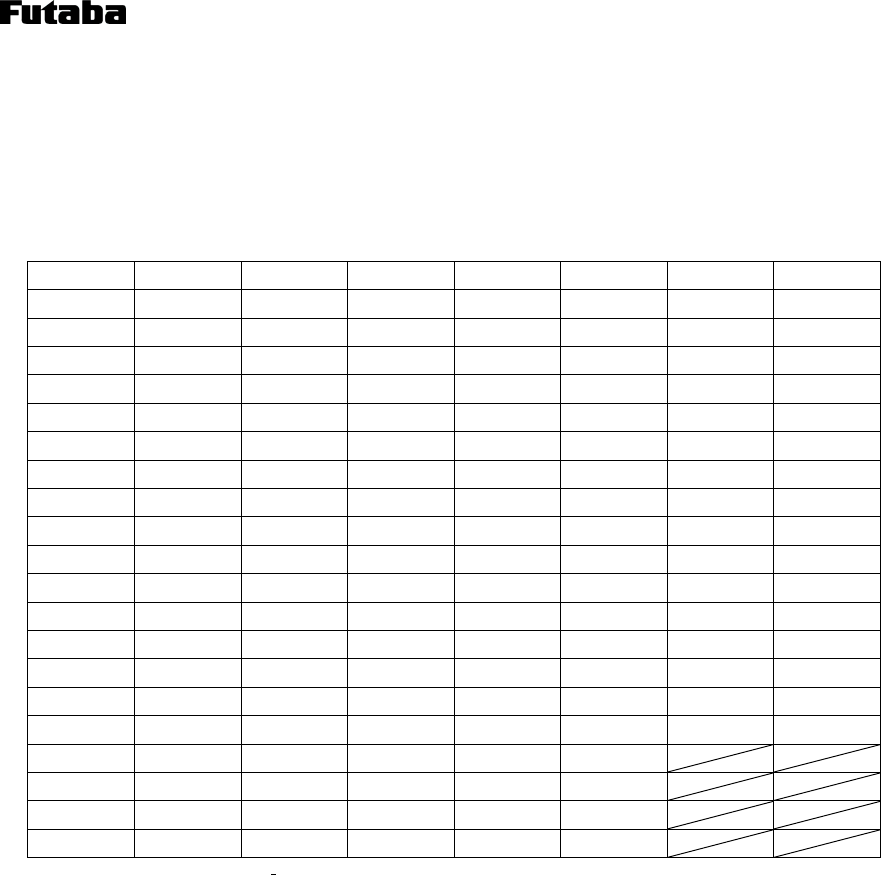
Ver.1.0
27
9. Frequency
9.1 Frequency Range
The available frequency range is from 2,402 MHz to 2477 MHz and it is divided into 76 channels. Below
table show a contrast between channel and frequency.
Channel Frequency Channel Frequency Channel Frequency Channel Frequency
02(02H) 2402MHz 22(16H) 2422MHz 42(2AH) 2442MHz 62(3EH) 2462MHz
03(03H) 2403MHz 23(17H) 2423MHz 43(2BH) 2443MHz 63(3FH) 2463MHz
04(04H) 2404MHz 24(18H) 2424MHz 44(2CH) 2444MHz 64(40H) 2464MHz
05(05H) 2405MHz 25(19H) 2425MHz 45(2DH) 2445MHz 65(41H) 2465MHz
06(06H) 2406MHz 26(1AH) 2426MHz 46(2EH) 2446MHz 66(42H) 2466MHz
07(07H) 2407MHz 27(1BH) 2427MHz 47(2FH) 2447MHz 67(43H) 2467MHz
08(08H) 2408MHz 28(1CH) 2428MHz 48(30H) 2448MHz 68(44H) 2468MHz
09(09H) 2409MHz 29(1DH) 2429MHz 49(31H) 2449MHz 69(45H) 2469MHz
10(0AH) 2410MHz 30(1EH) 2430MHz 50(32H) 2450MHz 70(46H) 2470MHz
11(0BH) 2411MHz 31(1FH) 2431MHz 51(33H) 2451MHz 71(47H) 2471MHz
12(0CH) 2412MHz 32(20H) 2432MHz 52(34H) 2452MHz 72(48H) 2472MHz
13(0DH) 2413MHz 33(21H) 2433MHz 53(35H) 2453MHz 73(49H) 2473MHz
14(0EH) 2414MHz 34(22H) 2434MHz 54(36H) 2454MHz 74(4AH) 2474MHz
15(0FH) 2415MHz 35(23H) 2435MHz 55(37H) 2455MHz 75(4BH) 2475MHz
16(10H) 2416MHz 36(24H) 2436MHz 56(38H) 2456MHz 76(4CH) 2476MHz
17(11H) 2417MHz 37(25H) 2437MHz 57(39H) 2457MHz 77(4DH) 2477MHz
18(12H) 2418MHz 38(26H) 2438MHz 58(3AH) 2458MHz
19(13H) 2419MHz 39(27H) 2439MHz 59(3BH) 2459MHz
20(14H) 2420MHz 40(28H) 2440MHz 60(3CH) 2460MHz
21(15H) 2421MHz 41(29H) 2441MHz 61(3DH) 2461MHz
( ): Hexadecimal indication.
Ver.1.0
28
9.2 Frequency Setting and Frequency Group
The FDP03 can use maximum 3 frequency channels as a one group. It can be set by REG06 to REG09.
For more details, refer to section 4.2.
Below tables show some examples.
Setting example 1
REG06 REG07 REG08 REG09
03H 02H 2AH 4DH
3-band mode 2402MHz 2442MHz 2477MHz
With the above settings, the FDP03 uses 3 frequency channels, 02H (2,402MHz), 2AH (2,442MHz) and
4DH (2477MHz), as a group. The FDP03 automatically selects the best channel of the wireless condition.
Setting example 2
REG06 REG07 REG08 REG09
01H 4FH 2AH 4DH
1-band mode 2479MHz 2442MHz 2477MHz
With the above settings, the FDP03 uses only 2,479MHz for communication.
Setting example 3
REG06 REG07 REG08 REG09
02H 2AH 2AH 4DH
2-band mode 2442MHz 2442MHz 2477MHz
With the above settings, the FDP03 uses 2 frequency channels that set by REG07 and REG08. However,
the FDP03 is uses only 2,442MHz because REG07 and REG08 are set to same channel.
When multiple FDP03 systems are operated in the same area, the
frequency channels should be apart at least 2 MHz to avoid the
interference from other systems.

Ver.1.0
29
9.3 Commands
The host system communicates to the FDP03 by below command.
9.3.1 List of commands
The table below shows the commands.
Command Function Remark
ARG Show the settings of all registers.
BCL Clear transmission and reception buffers.
DAS Show/set the destination address.
FNU Show/set the frequency group. Groups (1 to 3)
FRQ Show/set the frequency channel. Frequencies (02 to 77)
IDR Show ID code
IDW Set ID code
INI Initialize all memory registers.
RST Reset the FDP03.
REG Show/set the memory register REG00 to REG26
POF Release low power stand-by mode
PON Set low power stand-by mode
PTE Show/Set extended stand-by time
PTN Show/Set stand-by time
PTS Show/Set sleep time
ROF RF circuit OFF
RON RF circuit ON
SPD Show/set data transfer mode Transfer mode (1 or 2)
TBN Transmit binary data.
TID Show the serial number.
TS2 Execute a communication test.
TXT Transmit text data.
VER Show version information.
9.3.2 Command input format
The input format of a command is as follows:
@xxxx<Cr><Lf> @: Command header
xxxx: Command code
<Cr>: Carriage return code
<Lf>: Line feed code
If multiple commands are entered continuously, the commands that are entered
before the response from the FDP03 is ignored. Therefore, it should be entered
after the FDP03 returns a response for previous command.

Ver.1.0
30
9.3.3 Explanation of commands
ARG (Show all registers)
[Format]
ARG
[Response]
List of register settings (REG00 to REG26)
N0: Command error
[Function]
- The FDP03 returns all register settings by this command.
- The register settings are shown in hexadecimal code.
[Examples of use]
>@ARG<Cr><Lf>
<REG00: 00H<Cr><Lf>
<REG01: F0H<Cr><Lf>
・
・
・
<REG26: 01H<Cr><Lf>
BCL (Clear transmission and reception buffers)
[Format]
BCL
[Response]
P0: Normal end
N0: Command error
[Function]
- The transmission and reception buffer is cleared by this command.
[Examples of use]
>@BCL<Cr><Lf>
<P0<Cr><Lf>
If this command is executed during data transmission in broadcast transmission
mode, newly in coming data might be stored and output after the buffer is
cleared.
Also, serial data output is stopped when this command is executed during serial
data output.

Ver.1.0
31
DAS (Show/set the destination address)
[Format]
DAS (setting value)
setting value: 000 to 255
[Response]
xxx: Current address (in case of address referencing)
P0: Normal end (in case of address setting)
N0: Command error
[Function]
- This command shows and/or sets the destination address of headerless packet transmission mode.
- When this command is entered without any setting values, the FDP03 returns current destination address.
If setting value (new address) is put after DAS command, the destination address of the FDP03 is changed
to new one.
- Setting of a new address by this command is temporary. If the FDP03 is reset by RST command or
initialized, the destination address is returned to the address that is defined by REG02.
[Examples of use]
>@DAS<Cr><Lf>: Show current destination address
<003<Cr><Lf>: Current destination address is “003”.
>@DAS001<Cr><Lf>: Set the destination address to “001”.
<P0<Cr><Lf>: The destination address is changed normally.

Ver.1.0
32
FNU (Show/set a frequency group)
[Format]
FNU (frequency-group)
Available “frequency-group”: 1 to 3
[Response]
x: Currently set value
P0: Normal end
N0: Command error
[Function]
- This command shows or sets the frequency group.
- When this command is executed without setting value, current value is recalled.
- Available setting value "x" is 1 to 3. "1" indicates 1 channel mode (fixed frequency channel), "2" means
2 channel mode, and "3" represents 3 channel mode.
- Frequency group setting by this command is temporary. Thus, the setting is returned to that of REG06
after executing RST command or resetting FDP03. For permanent setting, the REG06 should be
changed.
“x”
(Setting
Va lu e )
Description
1 1 channel mode. Frequency channel that defined by REG07 is used.
2 2 channel mode. Frequency channels that defined by REG07 and REG08 are used.
3 3 channel mode. Frequency channels that defined by REG07, REG08 and REG09
are used.
[Examples of use]
>@FNU<Cr><Lf>: This command recalls the current set frequency group.
<3<Cr><Lf>: This response indicates the current set value is "3" (3-band mode).
>@FNU1<Cr><Lf>: This command sets the frequency group to the 1-band mode (1).
<P0<Cr><Lf>: This response indicates the normal end of command processing.
Ver.1.0
33
FRQ (Show/set frequency channel)
[Format]
FRQ (number) (:frequency channel)
Available “number”: 1 to 3
Available “frequency channel”: 02 to 77
[Response]
yy: Current frequency channel (02 to 77)
P0: Normal end
N0: Command error
[Function]
- This command indicates or sets a frequency channel.
- When this command is executed without “frequency channel”, current frequency channel is recalled.
- Frequency channel setting by this command is temporary. Thus, the setting is returned to that of REG07,
REG08 and REG09 after executing RST command or resetting FDP03. For permanent setting, the
REG07, REG08 and REG09 should be changed.
Available setting value of "number" is 1 to 3. "1" indicates the frequency channel set of REG07, "2"
indicates the frequency channel set of REG08, and "3" indicates the frequency channel set of REG09.
“number” Description
1 Frequency channel of REG07
2 Frequency channel of REG08
3 Frequency channel of REG09
[Examples of use]
>@FRQ1<Cr><Lf>: This command recalls the frequency channel of “frequency cannel 1”.
<02<Cr><Lf>: This response indicates the current t frequency channel is 02 (2,402MHz).
>@FRQ2:15<Cr><Lf>: This command sets the “frequency channel 2” to channel “15” (2,415MHz).
<P0<Cr><Lf>: This response indicates the normal end of command processing.

Ver.1.0
34
IDR (Show ID code)
[Format]
IDR
[Response]
xxxxH: Current setting value
(It is the value of REG04 and REG05 right after turned ON the main power.)
[Function]
- This command shows the ID code.
[Example of use]
>@IDR<Cr><Lf>: This command shows the ID code.
<0000H<Cr>Lf>: This response indicates the current ID code is “0000H”.
IDW (Set ID code)
[Format]
IDW
Available setting value: “0000H” to “FFFFFH”
[Response]
P0: Normal end
N0: Command error
[Function]
- This command can change ID code temporarily. For permanent change, REG04 and REG05 should be
changed.
[Example of use]
>@IDW1234H<Cr><Lf>: This command set ID code to 1234.
<P0<Cr>Lf>: Normal end.
Ver.1.0
35
INI (initializing memory registers)
[Format]
INI
[Response]
P0: Normal end
N0: Command error
[Function]
- This command resets all memory registers of the FDP03 to initial settings.
- All register settings that are customized are vanished.
[Example of use]
>@INI<Cr><Lf>: This command initializes all memory registers.
<P0<Cr>Lf>: This response indicates the normal end of command processing.
The host cannot receive any response from the FDP03 if a
communication parameters such as baud rate are different from default
setting.
It will take 520ms at maximum for P0 response of this command.
Memory registers may get damages if the power of FDP03 is turned
off before the P0 response comes back.
Ver.1.0
36
REG (Show/set memory registers)
[Format]
REG (register-number) (:setting value)
register-number: 00 to 26
setting value: 00H to FFH (000 to 255)
[Response]
xxH: Current value
P0: Normal end
N0: Command error
[Function]
- This command recalls setting value of memory register and/or sets a value of memory register.
- Available setting value of “register number” is 00 to 26.
- When this command is executed without “setting value”, current value of the defined register is recalled.
- “setting value” should be 3 digit decimal value or 2 digit hexadecimal value . If it is hexadecimal value,
“H” should be added at the end of the value.
[Examples of use]
>@REG00<Cr><Lf>: This command recalls the value of REG00.
<00H<Cr><Lf>: This response indicates the current value is “00H”.
>@REG00:001<Cr><Lf>: This command sets value of REG00 to 001
<P0<Cr><Lf>: This response indicates the normal end of command processing.
After executing this command to set a new value for a register, be sure
to execute the RST command. If you turn off the power of the
FDP03 before executing the RST command, the new setting of the
register will not be reflected to the FDP03.
It will take 520ms at maximum for P0 response of this command.
Ver.1.0
37
RST (resetting the FDP03)
[Format]
RST
[Response]
P0: Normal end
N0: Command error
[Function]
- This command has the following two functions:
(1) If values of the memory registers are changed before this command is executed, new register settings
are registered by this command execution. However, values that are changed by “DAS”, “FUN”
and “FRQ” command are vanished and the settings of memory registers are effective.
(2) This command also makes the FDP03 exit from the line quality test of the “TS2” command. When
this command is executed for exit from the line quality test, the memory register settings that are
made before execution of the TS2 command are not saved.
[Example of use]
>@RST<Cr><Lf>: This command resets the FDP03.
<P0<Cr><Lf>: This response indicates the normal end of command processing.
The host cannot receive any response from the FDP03 if
communication parameters such as baud rate are different from default
setting.
It will take 520ms at maximum for P0 response of this command.
Memory registers may get damages if the power of FDP03 is turned
off before the P0 response comes back.

Ver.1.0
38
POF (Release low power stand-by mode)
[Format]
POF
[Response]
P0: Normal end
N0: Command error
[Function]
- The operation mode is returned from “Low power stand-by mode” to “Normal operation mode” by this
command.
[Example of use]
>@POF<Cr><Lf>: Release low power stand-by mode.
<P0<Cr>Lf>: Normal end.
N0 response is returned if this command is executed during normal
operation mode.
PON (Set low power stand-by mode)
[Format]
PON
[Response]
P0: Normal end
N0: Command error
[Function]
- The operation mode is set to “Low power stand-by mode..
[Example of use]
>@PON<Cr><Lf>: Set low power stand-by mode.
<P0<Cr>Lf>: Normal end.
N0 response is returned if this command is executed during low power
stand-by mode.

Ver.1.0
39
PTE (Show/Set extended stand-by time)
[Format]
PTE(:setting value)
Available setting value: 000 to 015
[Response]
xxx: Current setting value (as referring the value)
P0: Normal end (as setting the value)
N0: Command error
[Function]
- This command can refer and/or set the time duration of the extended stand-by time. The extended
stand-by time duration is the setting value of this command times 20ms. For example, if the setting
value is 010, the extended stand-by time duration is 200ms (010 x 20ms). If the setting value is 000, the
extended stand-by time is not available.
[Example of use]
>@PTE<Cr><Lf>: Show current setting value
<003<Cr>Lf>: The setting value is 003. It means that the extended stand-by time duration is
60ms (003 x 20ms).
>@PTE015<Cr><Lf>: Set the extended stand-by time duration to 300ms (015 x 20ms).
<P0<Cr><Lf> : Normal end.
If the data packet is sent by broadcasting mode and/or the address
check function (REG18) setting is “Disabling group address check at
reception”, the FDP03 does not turn to the “Extended Stand-by mode” even if
the extended time duration is set.
PTN (Show/Set stand-by time)
[Format]
PTN(:setting value)
Available setting value: 001 to 255
[Response]
xxx: Current setting value (as referring the value)
P0: Normal end (as setting the value)
N0: Command error
[Function]
- This command can refer and/or set the time duration of the stand-by time. During the stand-by time, the
RF circuit is turned on. The stand-by time duration is the setting value of this command times 10ms.
For instance, if the setting value is 010, the extended stand-by time duration is 100ms (010 x 10ms).
[Example of use]
>@PTN<Cr><Lf>: Show current setting value
<003<Cr>Lf>: The setting value is 005. It means that the stand-by time duration is 50ms (005
x 10ms).
>@PTN007<Cr><Lf>: Set the extended stand-by time duration to 70ms (007 x 10ms).
<P0<Cr><Lf> : Normal end.

Ver.1.0
40
PTS (Show/Set sleep time)
[Format]
PTS(:setting value)
Available setting value: 001 to 255
[Response]
xxx: Current setting value (as referring the value)
P0: Normal end (as setting the value)
N0: Command error
[Function]
- This command can refer and/or set the time duration of the sleep time. The sleep time duration is the
setting value of this command times 10ms if the setting of bit 1 of RGE24 is “0”. Also, it is the setting
value of this command times 100ms if the setting of bit 1 of RGE24 is “1”. For example, if the setting
value is 030 and the setting of bit 1 of REG24 is “0”, the sleep time duration is 30ms (030 x 10ms). If
the setting value is 050 and the setting of bit 1 of REG24 is “1”, the sleep time duration is 500ms (050 x
100ms).
[Example of use]
>@PTS<Cr><Lf>: Show current setting value
<025<Cr>Lf>: The setting value is 025. It means that sleep time is 250ms (as bit 1 of REG24
is “0”) or 2500ms (as bit 1 of REG24 is “1”).
>@PTS010<Cr><Lf>: Set the sleep time duration to 100ms (as bit 1 of REG24 is “0”) or 1000ms (as bit
1 of REG24 is “1”).
<P0<Cr><Lf> : Normal end.
ROF (RF circuit OFF)
[Format]
ROF
[Response]
P0: Normal end
N0: Command error
[Function]
- This command turns off the RF circuit. If the RF circuit has been already turned off, N0 response is
returned after executing this command.
[Example of use]
>@ROF<Cr><Lf>: Turn off the RF circuit.
<P0<Cr><Lf> : Normal end.
During the RF circuit is turned off, @TXT and @TBN command are not
available.

Ver.1.0
41
RON (RF circuit ON)
[Format]
RON
[Response]
P0: Normal end
N0: Command error
[Function]
- This command turns on the RF circuit. If the RF circuit has been already turned on, N0 response is
returned after executing this command.
[Example of use]
>@RON<Cr><Lf>: Turn on the RF circuit.
<P0<Cr><Lf> : Normal end.
SPD (Show/set data transfer mode)
[Format]
SPD(: Data transfer mode)
Data transfer mode: 1 or 2
[Response]
x: Current setting value
P0: Normal end
N0: Command error
[Function]
- This command show and/set data transfer mode.
- The data transfer mode is “Interchange” mode if the setting value is “1”.
- The data transfer mode is “Communication Distance Extend” mode if the setting value is “2”.
- Setting of the data transfer mode by this command is temporary. If the FDP03 is reset by RST
command or initialized, the mode is returned to the setting of the bit 5 of the REG10.
x (Setting Value) Data Transfer Mode
1 Interchange Mode
2 Communication Distance Extend Mode
[Example of use]
>@SPD<Cr><Lf>: Show the data transfer mode.
<1<Cr><Lf> : The mode is “Interchange” mode.
>@SPD2<Cr><Lf>: Set the data transfer mode to “Communication Distance Extend” mode.
<P0<Cr><Lf> : Normal end.
The data transfer mode should be same setting among communication
partners. If the mode is different each other, it is impossible to
communicate with.

Ver.1.0
42
TBN (transmit binary data)
[Format]
TBN (destination-address) (length-of-message-bytes) (message)
- destination-address: 000 to 239
240 to 254 (for group communication)
255 (for broadcast transmission)
- length-of-message-bytes: 000 to 130
- message: Arbitrary binary data (130 bytes or less)
[Response]
P0: Normal end
P1: Command is accepted and data are being transmitted
N0: Command error
N1: Data transmission is failed. (The radio modem at the destination address does not respond or
transmission cannot be started because of carrier sensing.)
N3: Data transmission is failed because the receiving data buffer of the destination modem is full.
[Function]
- This command transmits binary data.
- The length of message can be defined from 0 to 130 bytes arbitrary.
- To broadcast data to multiple radio modems, “destination address” should be defined to “255”. At this
setting, the sender FDP03 transmits data packet “re-transmission frequency” that is defined by REG11 + 1
times and then returns P1 and/or P0 response to the host according to the REG13 setting.
[Examples of use]
>@TBN001005HELLO<Cr><Lf>: The FDP03 sends the message “HELLO” to the destination modem
that wireless address is “001” by this command.
<P1<Cr><Lf>: This response indicates that the command is accepted and the data is
being transmitted.
<P0<Cr><Lf>: This response indicates the normal end of command processing.
>@TBN002005HELLO<Cr><Lf>: The FDP03 sends the message “HELLO” to the destination modem
that wireless address is “002” by this command.
<P1<Cr><Lf>: This response indicates that the command is accepted and the data is
being transmitted.
<N1<Cr><Lf>: This response indicates that transmission is failed because the
destination modem that wireless address is “002” did not respond or
the data transmission was not started by carrier sensing.
The length of message should be not more than 130 bytes. It becomes
command error if the length of message exceeds 130 bytes.
The delimiter of this command should be “<Cr><Lf>”. It becomes command
error if different delimiter is added.
At broadcast transmission mode, the sender FDP03 cannot recognize whether
receiver FDP03s receive the transmitted data or not.
Do NOT execute next command before the sender FDP03 receives P0 response.
If the setting is "Disabling response" and no P0 response is sent to the sender
FDP03, please wait expected P0 response time before executing next command.
If next command is executed before P0 response, command error is occurred and
the system might have unexpected movement.

Ver.1.0
43
TID (show the serial number)
[Format]
TID
[Response]
xxxxxxxxx: 9-digit serial number
N0: Command error
[Function]
The FDP03 replies its 9 digits serial number when this command is executed.
If it is failed to read the serial number, the FDP03 returns “?”.
[Example of use]
>@TID<Cr><Lf>: This command requests to show the serial number of the FDP03.
< xxxxxxxxx <Cr><Lf>: This response indicates the serial number of the FDP03.
TS2 (executing a communication line quality test)
[Format]
TS2
[Response]
P0: Command accepted
Connect: Line connected and line quality test is started
ooooo....ooxo 003: Test result
Disconnect: Line disconnected
N0: Command error
[Function]
- The communication line quality test is executed by this command. At the test, one data packet has 32
bytes and one hundred packets are exchanged as a test unit between the “master” FDP03 and the
“slave” FDP03. The test results are output to the serial port.
- The test result is shown by “o” and “x” for each packet. “o” indicates that it is no communication
error and “x” indicates that communication error is occurred.
- When this command is executed at the “master” FDP03, the “master” tries to connect the “slave”
FDP03 that wireless address is defined by REG02 of the “master”. At that time, operation mode of the
“slave” is automatically changed to TS2 communication line quality test mode.
- Both the “master” and the “slave” output the test result.
- Total error occurrence of the test is indicated in 3 digits number after 100 of “o” ”x” judgments.
- If consecutive 1,000 packets become communication error, the line is disconnected. After the
disconnection, the “master” continues to request wireless connection but the “slave” abort from TS2 test
mode.
- During this TS2 test mode, all the commands except for “FUN”, “FRQ” and “RST” command are do
not work. For abort from TS2 test mode, it is needed to execute “RST” command or turned off the
main power of the FDP03. When the “master” aborts from TS2 test mode, the “slave” automatically
stops the test mode and returns to normal operation mode.
[Example of use]
>@TS2<Cr><Lf>: The FDP03 runs communication test by this command.
<P0<Cr><Lf>: This response indicates that the command is accepted.
<Connect<Cr><Lf>: This response indicates that the line is connected.
<xooooooooo...ooox 003<Cr><Lf>: This response indicates the test result and 3 packets became
communication errors during 100 packet correspondences.
<oooxoooooo...oxoo 002<Cr><Lf>: This response indicates the test result and 2packets became
communication errors during 100 packet correspondences.
<oooooooxxo...ooxo 004<Cr><Lf>: This response indicates the test result and 4 packets became
communication errors during 100 packet correspondences.
<ooxxxooooo...oxoo 006<Cr><Lf>: This response indicates the test result and 6 packets became
communication errors during 100 packet correspondences.

Ver.1.0
44
TXT (transmit text data)
[Format]
TXT (destination-address) (message)
- destination-address: 000 to 239
240 to 254 (for group communication)
255 (for broadcast transmission)
- message: Arbitrary binary data (130 bytes or less)
[Response]
P0: Normal end
P1: Command is accepted and data are being transmitted
N0: Command error
N1: Data transmission is failed. (The radio modem at the destination address does not respond or
transmission cannot be started because of carrier sensing.)
[Function]
- This command orders the FDP03 to transmit text data.
- The length of message can be defined from 0 to 130 bytes and a delimiter indicates the end of message
data.
- To broadcast data to multiple radio modems, “destination address” should be defined to “255”. At this
setting, the sender FDP03 transmits data packet “re-transmission frequency” that is defined by REG11 + 1
times and then returns P1 and/or P0 response to the host according to the REG13 setting.
[Examples of use]
>@TXT001HELLO<Cr><Lf>: The FDP03 sends the message “HELLO” to the destination modem that
wireless address is “001” by this command.
<P1<Cr><Lf>: This response indicates that the command is accepted and the data is being
transmitted.
<P0<Cr><Lf>: This response indicates the normal end of command processing.
>@TXT002HELLO<Cr><Lf>: The FDP03 sends the message “HELLO” to the destination modem that
wireless address is “002” by this command.
<P1<Cr><Lf>: This response indicates that the command is accepted and the data is being
transmitted.
<N1<Cr><Lf>: This response indicates that transmission is failed because the destination
modem that wireless address is “002” did not respond or the data
transmission was not started by carrier sensing.
The length of message should be not more than 130 bytes. It becomes
command error if the length of message exceeds 130 bytes.
If the message includes "<Cr><Lf>," the FDP03 is recognizes that it is the
end of the message and it ignores following message. Thus, “TBN”
command should be used instead of “TXT” command if the message
contains “<Cr><Lf>”.
At broadcast transmission mode, the sender FDP03 cannot recognize
whether receiver FDP03s receive the transmitted data or not.
Do NOT execute next command before the sender FDP03 receives P0
response. If the setting is "Disabling response" and no P0 response is
sent to the sender FDP03, please wait expected P0 response time before

Ver.1.0
45
executing next command. If next command is executed before P0
response, command error is occurred and the system might have
unexpected movement.

Ver.1.0
46
VER (reading version information)
[Format]
VER
[Response]
Version information
N0: Command error
[Function]
The FDP03 shows the version of the system.
[Example of use]
>@VER<Cr><Lf>: This command orders to show the version information from the FDP03.
<Version 01.00<Cr><Lf>: This response indicates that the system version of the FDP03 is 1.00.
Ver.1.0
47
10. Interface
10.1. Pin Layout
Pin No. Pin name Input/output Remark
1 Vcc - Power supply (3.3 to 5.5 VDC)
2 RXD OUT Data output
3 TXD IN Data input
4 CTS OUT Hardware flow control
5 RTS IN Hardware flow control
6 TEST - (Leave this pin unconnected.)
7 /INI IN Parameter initialization
8 /SHUT IN Power-off
9 TEST - (Leave this pin unconnected.)
10 GND - Ground
Explanation of the pins
Vcc: Power supply pin. Connect a power source and the voltage range is from 2.5 to 5.5 VDC.
RXD: Data output pin that is the DCE compliant
TXD: Data input pin that is the DCE compliant
CTS: Hardware flow control output pin that is the DCE compliant (Hardware flow control is enabled
when the signal is high level.)
RTS: Hardware flow control input pin that is the DCE compliant (Hardware flow control is enabled
when the signal is high level.)
/INI: Parameter initialization pin. Leave this pin unconnected when it is not used. To initialize the
registers, set the /INI pin to low level at power-on or combine the operation of this pin with the
operation of the /SHUT pin. After the registers (parameters) are initialized, the DP01 operates in
normal mode.
/SHUT: Power-off pin. When this pin is set to low level, the main power of the FDP03 is cut and becomes
“power-down” mode. When the setting of this pin is high level, the FDP03 is in normal operation
mode.
TEST: Test pin. Do NOT use this pin. This pin is only for maintenance by the manufacturer.
GND: Ground pin
Parameter setting of the register will be vanished if the /SHUT pin
becomes low level and the operation mode becomes “power-down”
mode. Therefore, DO NOT connect /SHUT pin during REG
command setting.
After releasing from the power-down mode, parameter settings of
registers that were changed by commands will be initialized. Thus,
the parameter settings should be done by the memory registers when
the “power-down” mode is used or set the parameters again after
returning from the “power-down” mode.
It will take 90 ms at the maximum to return from the “power-down”
mode to normal operation mode.
10.2. Recommended Connector
Hirose Electric Co., Ltd. DF12E(3.0)-10DP-0.5V
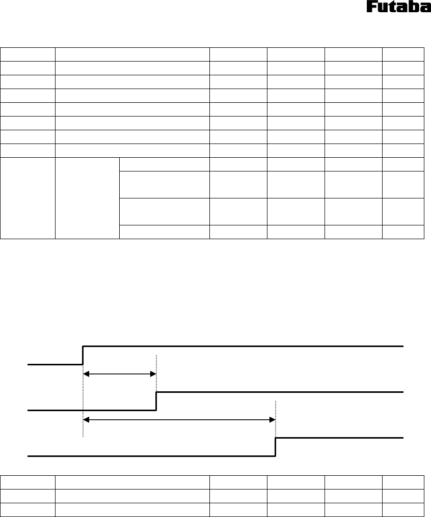
Ver.1.0
48
10.3. Electrical Characteristics
Symbol Item Minimum Typical Maximum Unit
VCC Power supply voltage 2.5 - 5.5 V
VIH High-level input voltage 1.6 2.2 V
VIL Low-level input voltage 0 - 0.5 V
VIH(/SHUT) High-level input voltage at /SHUT pin 1.45 Vcc V
VIL(/SHUT) Low-level input voltage at /SHUT pin 0 - 0.25 V
VOH High-level output voltage 1.9 - 2.2 V
VOL Low-level output voltage 0 - 0.2 V
Normal Mode - - 45 mA
Low Power Stand-by
Mode - - 2 mA
RF Circuit Power
Control Mode - - 2 mA
ICC
Power supply
current
Power Down Mode - 3 5 uA
10.4. AC Characteristics
10.4.1. Main Power On
Symbol Item Minimum Typical Maximum Unit
TWAKE Serial circuit wake-up time delay - - 20 mS
TRF RF circuit wake-up time delay - - 90 mS
Power
Serial Circuit
RF Circuit
TWAKE
TRF
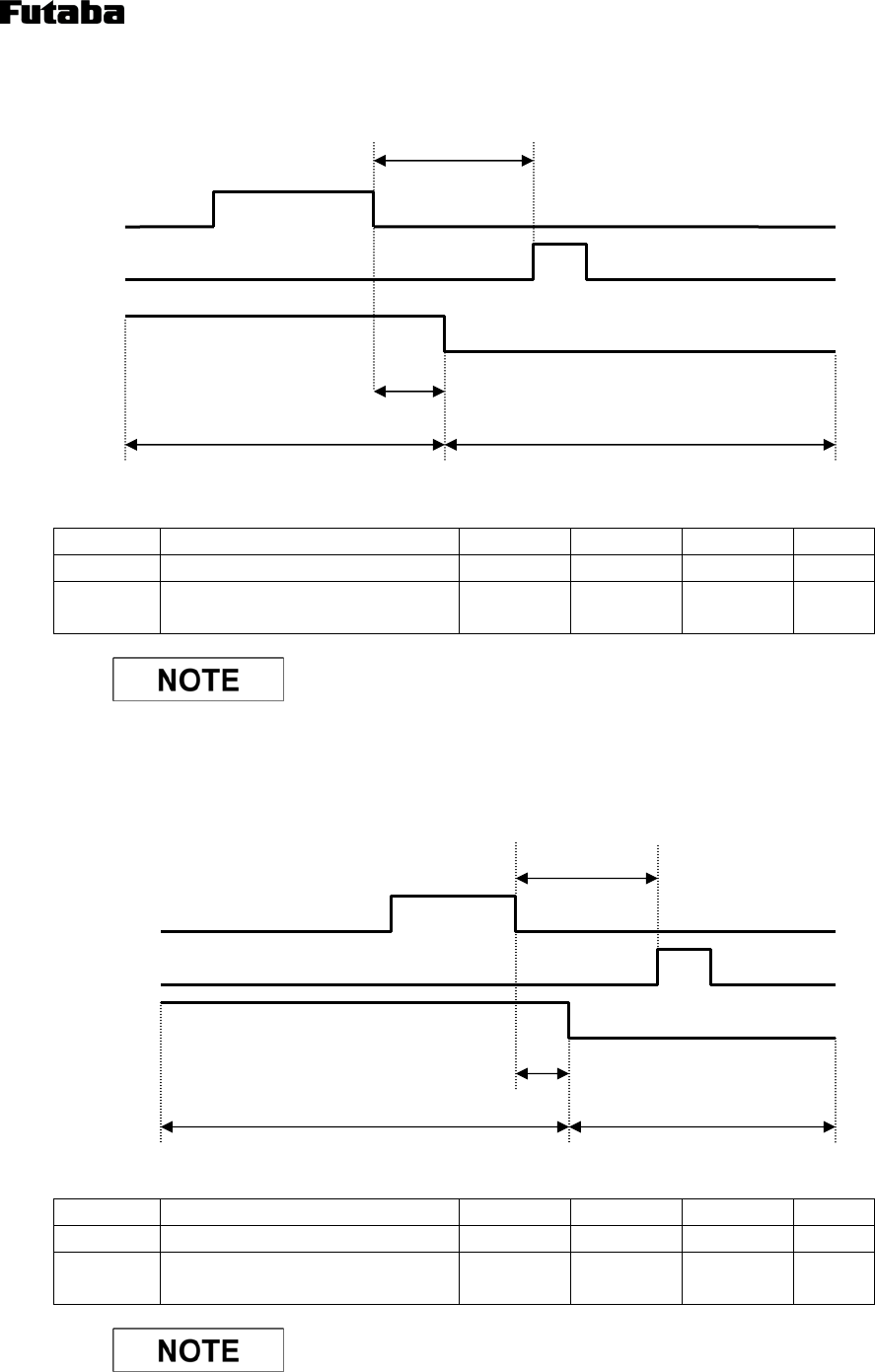
Ver.1.0
49
10.4.2 Low Power Stand-by Mode
10.4.2.1 Transition to low power stand-by mode by PON command
Symbol Item Minimum Typical Maximum Unit
TLPRES Response time delay of serial circuit - - 1 mS
TLPON Transition time to low power stand-by
mode - - 340 uS
A command for sending data packet is available after receiving P0
response.
10.4.2.2 Transition from low power stand-by mode to normal operation mode by POF command
Symbol Item Minimum Typical Maximum Unit
TLPRES Response time delay of serial circuit - - 1 mS
TLPON Transition time to normal operation
mode - - 340 uS
A command for sending data packet is available after receiving P0
response.
Serial RX
Serial TX
Operation Mode
@PON
P0
TLPRES
TLPON
Normal Operation Mode Low Power Stand-by Mode
@POF
P0
TLPRES
TLPOFF Normal Operation Mode Low Power Stand-by Mode
Serial RX
Serial TX
Operation Mode
Ver.1.0
50
10.4.2.3 Enable timing of data packet receiving during low power stand-by mode
Symbol Item Minimum Typical Maximum Unit
TRFON Time delay for wireless
communication - - 1 mS
TRFOFF Time difference of wireless
communication stop - - 340 uS
10.5.3. RF Circuit Power Control Mode
10.5.3.1. Transition of RF circuit from RF Off to RF On
Symbol Item Minimum Typical Maximum Unit
TRFRES Response Time of Serial Circuit for
RF Control - - 1 mS
TRFON Transition Time for Operation Mode
Change - - 340 uS
A command for sending data packet is available after receiving P0
response.
Sleep Mode Stand-by Mode Sleep Mode
TRFON T
RFOFF
Wireless Communication
Is Enable
@RON
P0
TRFRES
TRFON
Wireless Communication Is Enable
Wireless Communication
Is NOT Enable
Serial RX
Serial TX
Status of Wireless Communication
Ver.1.0
51
10.5.3.2 Transition of RF circuit from RF On to RF Off
Symbol Item Minimum Typical Maximum Unit
TRFRES Response Time of Serial Circuit for
RF Control - - 1 mS
TRFOFF Transition Time for Operation Mode
Change - - 340 uS
A command for sending data packet is available after receiving P0
response.
10.5.4. Power Down Mode
Symbol Item Minimum Typical Maximum Unit
TW/SHUT Pulse Width of /SHUT 3 - - mS
T/SHUT Shut Down Time - - 500 uS
TWAEK Recovery Time of Serial Circuit - - 20 mS
TRF Enable Time Duration of Wireless
Communication - - 90 mS
@RON
P0
TRFRES
TRFOFF
Wireless Communication Is Enable Wireless Communication
Is NOT Enable
Serial RX
Serial TX
Status of Wireless Communication
TW/SHUT T
WAEK
T/SHUT TRF
/SHUT
Serial Circuit
Status of Wireless Communication
Ver.1.0
52
10.5.5. Parameter Initializing by /SHUT and /INI Terminal
Symbol Item Minimum Typical Maximum Unit
TW/SHUT Pulse Width of /SHUT 3 - - mS
Th/INI Hold Time of /INI Signal 0 - - mS
TWAIT Enable Time of /INI Signal 15 - - mS
T/SHUT Shut Down Time - - 500 uS
TWAEK Recovery Time of Serial Circuit - - 40 mS
TRF Enable Time Duration of Wireless
Communication - - 100 mS
It will take 90 ms at the maximum to return from the “power-down”
mode to normal operation mode.
When the parameters of FDP03 is initialized by /SHUT terminal and
/INI terminal, the serial circuit is ready in 40ms after /SHUT terminal
is set to “High” level. However, it will take 100ms to ready to the RF
circuit because the RF circuit checks communication acceptance.
TW/SHUT T
WAIT
Th/INI
TW/AEK
T/SHUT TRF
Ver.1.0
53
11. Product Specifications
11.1. Outer Dimensions
43 x 25 x 3 mm (excluding connectors)
11.2. Weight
Approximately 3.6 g
11.3. Power Supply
Voltage : 2.5 to 5.5 VDC
Current :
Operation Mode MIN. TYP. MAX. Unit
Normal Operation Mode - - 45 mA
Low Power Stand-by Mode - - 2 mA
RF Circuit Power Control Mode - - 2 mA
Power Down Mode - 3 5 uA
Chip Antenna (FDP03TJ020)
Interface Connector
Antenna Connector (FDP03TJ010)

Ver.1.0
54
11.4. Radio Specifications
Technical standard: ARIB STD-T66 (Japan)
FCC Part 15.237 (U.S.)
ETSI EN 300 328 V.1.7.1 (EU)
Certification number: 001NYDA1387 (Japan)
AZP-FDP03 (U.S.)
Communication method: FSK
Service area: 100m (“Interchange” mode: open-air line-of-sight distance)
200m (“Communication Distance Extend” mode: open-air line-of-sight
distance)
Transmission output power: 10 mW
Number of frequency channels: 76 (2,402 to 2477 MHz)
Line speed: 1 Mbps (“Interchange” mode),
250kbps (“Communication Distance Extend” mode)
Actual Throughput: 22kbps MAX. (if the line speed of the interface is 115.2kbps.)
Connector: U.FL made by Hirose Electric Co., Ltd.
Antenna: Connecter IPEX 20279-001E-01 (FDP03TJ010)
Built-in (FDP03TJ020)
10.5 Interface
Protocol: 2.2 V asynchronous (DCE specifications)
Line speed: 9,600, 19,200, 38,400, or 115,200 bps
Data length: 7 or 8 bits
Stop bit: 1 or 2 bits
Parity: Odd, even, or no parity
Connector: DF12C(3.0)-10DS-0.5V (Hirose Electric Co., Ltd.)
10.6 Environment
Operating temperature: -20℃ to 60℃
Storage temperature: -30℃ to 70℃
Operating humidity: 90% RH or less (without condensation)
Storage humidity: 90% RH or less (without condensation)
Vibration tolerance: Compliant with JIS-C-60068-2-6
Shock resistance: Compliant with JIS-C-60068-2-27

Ver.1.0
55
11. Notes
11.1 Data Communication Delay
It will take certain time to synchronize when the frequency group setting is 2 frequency channel mode or 3
frequency channel mode.
11.1.1 Delay at the transmission side
(1) Delay due to the number of frequency channels in use
When the setting of the FDP03 is 2 frequency channel mode and/or 3 frequency mode, the FDP03
changes the data transmission frequency channel as every data re-transmission. It takes 7.6 ms to
re-transmit a data packet for packet generation, carrier sensing and waiting ACK time-out. Thus, the
data communication will be delay when the setting of the FDP03 is 2 frequency channel mode and/or 3
frequency mode.
(2) Delay due to carrier sensing
If the FDP03 detects radio wave that is same frequency channel as own use, the FDP03 switches the
carrier frequency channel to another. It is called “carrier sensing” and takes 7.6 ms. Thus, the data
communication will be delayed if other wireless systems such as WiFi in the same area.
11.1.2 Delay at the reception side
(1) Delay due to extension of reception-wait time
The FDP03 extends reception-wait time according to the frequency it has received. The extended
reception-wait time depends on the on the number of frequencies in the frequency group, which is "10+5
x (number of frequencies in the frequency group)2" ms. Since the FDP03 keeps the same frequency
during the extended reception-wait time, the extension of reception-wait time may cause a delay in
communication in an environment with much noise or jamming.
11.2 Reception of Same Packets
The FDP03 can store five packets of received data in the reception data buffer. However, when it receives
more than 5 packets, the FDP03 deletes the data packet from the oldest data one after the other. For example,
if the local FDP03 receives data packets from six remote FDP03s at the same time, one of the received data
packet is eliminated. Therefore, when the FDP03 receives a data packet that is same as the eliminated one,
the FDP03 cannot realize the duplication of the data packet and output the data to the host. It will happen
when the FDP03 is used in below listed condition.
(1) More than seven or more FDP03s operate at the same time in the system.
(2) Data re-transmission is frequent.
(3) The data packets having the same packet size are transmitted.
Even if the local FDP03 cannot receive the ACK signal of a packet from the remote FDP03, the remote FDP03
may success to received the packet.
11.3 Timing of Command Input
Do NOT execute next command before the sender FDP03 receives P0 response. If the setting is "Disabling
response" and no P0 response is sent to the sender FDP03, please wait expected P0 response time before
executing next command. If next command is executed before P0 response, command error is occurred and
the system might have unexpected movement.
When "Disabling response" is defined, the command should be executed after waiting the specific time that is
defined by REG15.

Ver.1.0
56
11.4 Headerless Packet Transmission Mode
11.4.1 Input data
In headerless packet transmission mode, up to 150 bytes of message can be stored in the transmission buffer,
and transmission starts when the total length of the messages stored in the message buffer exceeds 26 bytes.
If many messages are input successively, the message buffer may become full because wireless transmission
cannot keep pace with message input, and some messages may be lost. If such an event occurs, enable the
hardware flow control. You are recommended to specify "Enabling response" also in headerless packet
transmission mode since, with this setting, you can confirm the success or failure in message transmission with
each response.
11.4.2 Measures against packet loss
(1) Messages exceeding 26 bytes
If messages not less than 26 bytes in total are input successively, transmission of some messages input
earlier may fail. To prepare for such an event, check each response on the sender FDP03 to prevent the
loss of messages, and create messages so that the loss of packets can be determined on the receiver
FDP03.
(2) Setting of serial communication speed
If different serial communication speeds are set on the sender FDP03 and the receiver FDP03, the loss of
data may occur on the FDP03 configured with a slower speed than that of the other FDP03. Therefore,
you are recommended to set the same serial communication speed on all FDP03s.
11.5 Occurrence of Data Loss Even under Hardware Flow Control
If the FDP03 is connected to a personal computer and a specific software program created on the personal
computer is used, the data output from the personal computer to the FDP03 does not stop immediately even
when the input to the FDP03 is disabled by hardware flow control. In such cases, the data output from the
personal computer may be lost.
11.6 Frequency Setting in Multi-System Environment
If multiple FDP03 systems are operating, set the radio frequencies that are apart from each other at least by 2
MHz on individual FDP03s. If adjacent communication channels are set on different FDP03s, interference
may occur and disable the FDP03s to communicate.
11.7 Timing of Command Input
When entering multiple commands successively, wait, after entering a command, until the P0 response for the
entered command is received before entering the next command. If the next command is entered before the
P0 response for the preceding command is received, an error occurs or the entered next command is ignored.
11.8 INI and RST Commands
After executing the INI or RST command, always check that the P0 response is returned. Turning off the
power of the FDP03 before the P0 response is returned may damage memory registers. If the return of P0
response cannot be checked, for example, in case that the baud rate has been initialized, wait for 520 ms or
more after entering the INI or RST command, and then turn off the power.
11.9 Power-Down Mode
Switching the FDP03 to the power-down mode (by setting the /SHUT pin to the low level) while registers of
the FDP03 are being accessed may delete the settings in the registers. To avoid this problem, do not control
the /SHUT pin while the REG command is being executed.
Releasing the FDP03 from the power-down mode clears the parameter settings in registers that were made
with commands before the FDP03 was set into the power-down mode. Change the parameter settings before
using the power-down mode, or make the parameter settings again after releasing the FDP03 from the
power-down mode.
The FDP03 returns to the normal operation in a maximum of 120 ms after the FDP03 is released from the
power-down mode.

Ver.1.0
How to obtain Help
Please contact Futaba technical support at the address shown below for:
Application information regarding the FDP or other Futaba products.
Technical Assistance or Training
Safety Questions
Additional manuals or other documentation
Repair or service for your Futaba products
Comments regarding the product or this manual
- Do not modify or disassemble the product.
* The specifications and external designs of this product may be changed for improvement without prior
notice.
* Futaba Corporation will not be liable for any damages resulting from the use of the product that has
been modified without prior consent of Futaba Corporation.
In Japan
Futaba Corporation
1080 Yabutsuka, Chosei-mura, Chosei, Chiba Prefecture 299-4395, Japan
Telephone: +81-475-32-2151, Fax: +81-475-32-6179
In United States
Futaba Corporation of America
711 E. State Parkway Schaumburg, Illinois 60173, U.S.A
TEL: +1-847-884-1444 FAX:+ 1-847-884-1635
In Europe
Futaba (Europe) GmbH
Halskestrasse 9, D-47877 Willich, Germany
TEL: +49-2154-943-0 FAX: +49-2154-943-200
In Asia
FUTABA DENSHI Corp. (S) Pte.Ltd.
152 Beach Road, The Gateway East, #23-08, Singapore 189721
TEL: +65-6291-9882 FAX: +65-6291-7391
For inquiries or more information, contact:
- Industrial Equipment Sales Unit, Radio Control Equipment Group, Futaba Corporation
1080 Yabutsuka, Chosei-mura, Chosei, Chiba Prefecture 299-4395, Japan
Telephone: 0475-32-6173
Facsimile: 0475-32-6179
- URL of Futaba's Website: http://www.futaba.co.jp
R
INSTRUCTIONS MANUAL
FEDERAL COMMUNICATIONS COMMISSION
INTERFERENCE STATEMENT
This equipment has been tested and found to comply with the limits for a Class B digital
device, pursuant to Part 15 of the FCC Rules. These limits are designed to provide
reasonable protection against harmful interference in a residential installation. This
equipment generates, uses, and can radiate radio frequency energy and, if not installed
and used according to the instructions, may cause harmful interference to radio
communications. However, there is no guarantee that interference will not occur in a
particular installation. If this equipment does cause harmful interference to radio or
television reception, which it found by turning the equipment off and on, the user is
encouraged to try to correct the interference by one or more of the following measures:
-- Reorient or relocate the receiving antenna.
-- Increase the separation between the equipment and receiver.
-- Connect the equipment into an outlet other than the receiver’s
-- Consult the dealer or an experienced radio/TV technician for assistance.
CAUTION:
To assure continued FCC compliance:
(1) Any changes or modifications not expressly approved by the grantee of this device
could void the user's authority to operate the equipment.
FCC Label Compliance Statement:
This device complies with Part 15 of the FCC Rules. Operation is subject to the
following two conditions: (1) this device may not cause harmful interference, and (2)
this device must accept any interference received, including interference that may
cause undesired operation.
Exposure to Radio Frequency Radiation
To comply with FCC RF exposure compliance requirements, a separation distance of at
least 20cm must be maintained between the antenna of this device and all persons. This
device must not be co-located or operating in conjunction with any other antenna or
transmitter.