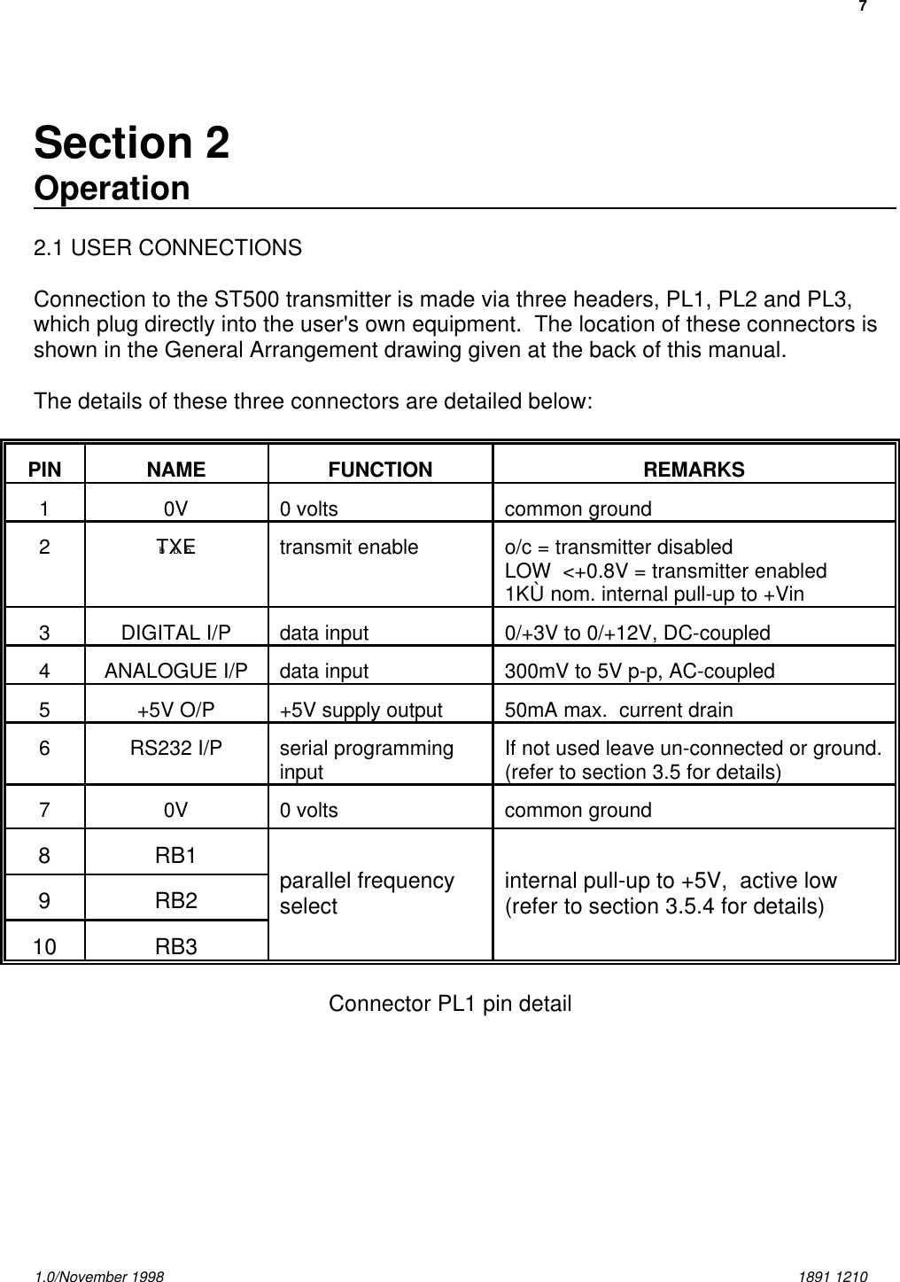
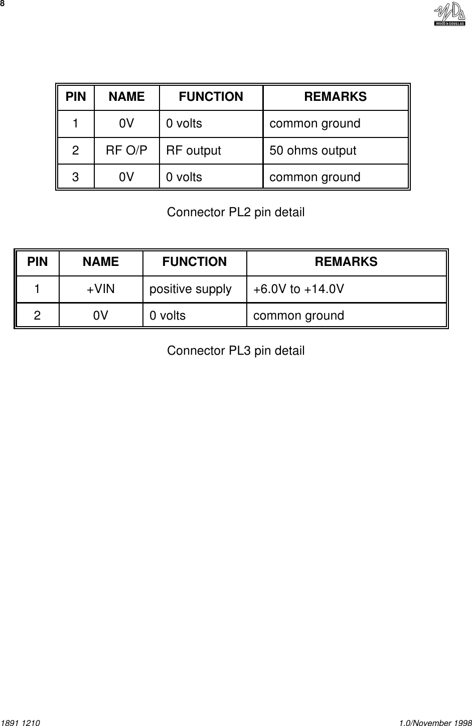
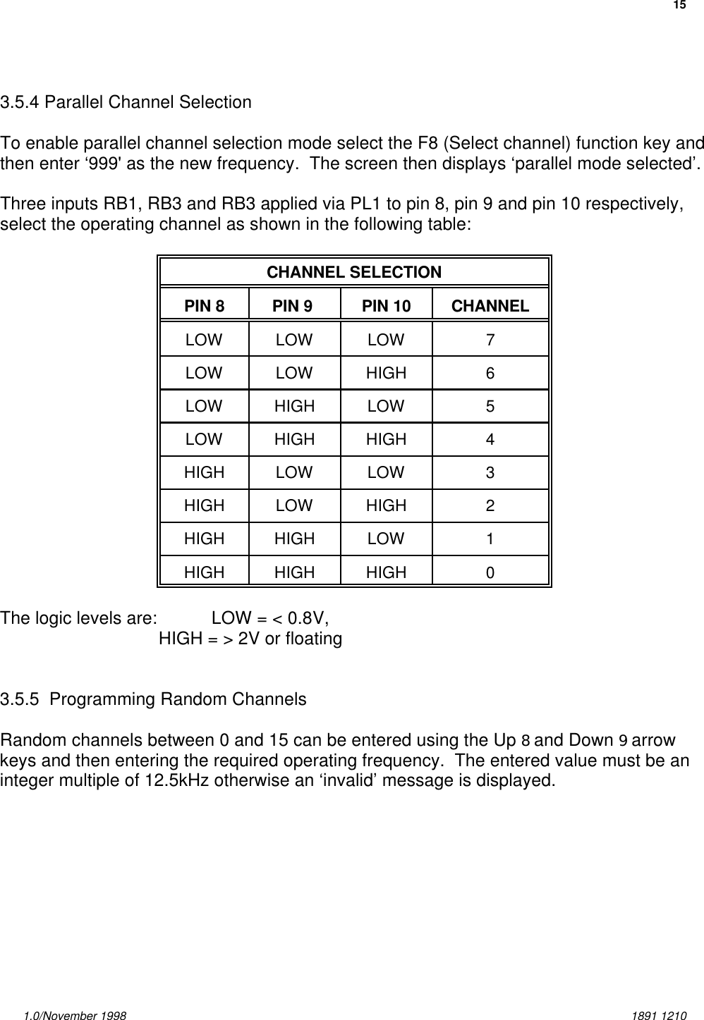
GE Medical Systems Information Technologies 340T Model 340 Medical Telemetry Transmitter User Manual TRANSMITTER

GE Medical Systems Information Technologies Inc. Model 340 Medical Telemetry Transmitter TRANSMITTER

Contents

Module User Manual

ST500TRANSMITTERTECHNICAL MANUAL(1891 1210)© Copyright Wood & Douglas Ltd 1998version: 1.0issue: November 1998LATTICE HOUSEBAUGHURST ROADTADLEYHAMPSHIREUK RG26 5LPTel: +44 (0)118 981 1444 Fax:+44 (0)118 981 1567
1.0/November 1998 1891 1210ContentsSection 1An overview .................................................51.1 GENERAL DESCRIPTION ...................................6Section 2Operation ...................................................72.1 USER CONNECTIONS ......................................7Section 3Technical description .........................................93.1 POWER SUPPLY ..........................................93.2 INPUT INTERFACE .........................................93.3 MODULATION STAGE ......................................93.4 RADIO FREQUENCY STAGE ................................103.5 FREQUENCY PROGRAMMING ..............................14Section 4Technical specifications ......................................19DRAWINGSWS1494/XX7 GENERAL ARRANGEMENT FOR ST500WD1632/001 CIRCUIT DIAGRAM FOR ST500 WD1632/XX2 COMPONENT OVERLAY FOR ST500 (Sheet 1 of 3)WD1632/XX2 COMPONENT OVERLAY FOR ST500 (Sheet 2 of 3)WD1632/XX2 COMPONENT OVERLAY FOR ST500 (Sheet 3 of 3)C WD632 00 ITEM LIST FOR LEADED COMPONENTS FOR ST500A SM1632 00 ITEM LIST FOR SURFACE MOUNT COMPONENTS FORST500
1891 1210 1.0/November 1998
51.0/November 1998 1891 1210Section 1An overviewWood & Douglas are an independent UK company dedicated to the design andmanufacture of high quality RF designs for the telemetry, security, broadcast and videomarkets world-wide.The information given in this manual is Copyright Wood & Douglas and is provided tothe original purchaser for the purposes of operation and routine maintenance.  Thecontents of this manual must not be disclosed to any third party, nor may the purchasermake additional copies of the manual or store the information given on any electronicretrieval or mass storage system.The company reserves the right to amend or change specifications of its productswithout prior notice in accordance with the company policy of continued productimprovement.NOTE:This device complies with Part 15 of the FCC Rules.Operation is subject to the condition that this device does not cause harmfulinterference.The unit is labelled with a serial number label as shown below:ST500 31 980912345FCC ID ABCST500    CECEwhere: 990912345 is the serial number of the unit containing the date code forSeptember 1998ABC is the Wood & Douglas Ltd FCC code
61891 1210 1.0/November 19981.1 GENERAL DESCRIPTIONThe ST500 can be configured for analogue or digital operation and is available in thefrequency range of 405 - 470MHz with a 12.5kHz channel spacing.The transmitter requires a nominal 12 volt DC supply connected via PL7.  Howeverthe unit will function correctly within the limits of +6.0V to +14.0V.  The output powerof the transmitter is normally preset to 100mW nominal.The ST500 is intended to fit into OEM equipment housing by means of the threeconnectors which protrude through the base of the unit.
71.0/November 1998 1891 1210Section 2Operation2.1 USER CONNECTIONSConnection to the ST500 transmitter is made via three headers, PL1, PL2 and PL3,which plug directly into the user's own equipment.  The location of these connectors isshown in the General Arrangement drawing given at the back of this manual.The details of these three connectors are detailed below:PIN NAME FUNCTION REMARKS10V 0 volts common ground2bTbXbEtransmit enable o/c = transmitter disabledLOW  <+0.8V = transmitter enabled1KÙ nom. internal pull-up to +Vin3DIGITAL I/P data input 0/+3V to 0/+12V, DC-coupled4ANALOGUE I/P data input 300mV to 5V p-p, AC-coupled5+5V O/P +5V supply output 50mA max.  current drain6RS232 I/P serial programminginput If not used leave un-connected or ground.(refer to section 3.5 for details)70V 0 volts common ground8RB1 parallel frequencyselect internal pull-up to +5V,  active low(refer to section 3.5.4 for details)9RB210 RB3Connector PL1 pin detail
81891 1210 1.0/November 1998PIN NAME FUNCTION REMARKS10V 0 volts common ground2RF O/P RF output 50 ohms output30V 0 volts common groundConnector PL2 pin detailPIN NAME FUNCTION REMARKS1+VIN positive supply +6.0V to +14.0V20V 0 volts common groundConnector PL3 pin detail
91.0/November 1998 1891 1210Section 3Technical descriptionRefer to the circuit diagram WD1632 at the rear of this manual.3.1 POWER SUPPLYDC power is connected to the transmitter module via PL3. The positive side of the supplyis fed to TR2 which acts as a series switch; when PL1 pin 2 is connected to 0V to enablethe transmitter then base current flows to TR2 via D6 and R54 and turns TR2 on.  Theoutput from the collector of TR2 (‘+Vraw’) is fed to dual operational amplifier IC4, to TR3collector (via chokes L5 and L6) and also to voltage regulator IC2.  This regulator providesa stable output of nominally +5V which is used to power all the remaining sections of thetransmitter (apart from IC7) either directly or via R-C decoupling networks.3.2 INPUT INTERFACEWhen the transmitter is to be used with an analogue modulation input then this input is fedfrom PL1 pin 4 via R2 and C2 to RV1 in the feedback network around IC1a. RV1 acts asan analogue gain control.When the transmitter is to be used with a digital modulation input then this input is fedfrom PL1 pin 3 via R1 to RV1 in the feedback network around IC1a.  RV1 is set mid-way inthis application such that it has no effect; IC1a then functions as a comparator andproduces an output which swings between approximately +0.7V and +4.3V depending onwhether the digital input is low or high. These output levels are well-defined and result inthe modulation level being independent of the logic levels at the input to the transmitter.3.3 MODULATION STAGEThe output from IC1a is fed to a low-pass filter built around IC1b. This restricts themodulation bandwidth such that adjacent channel power levels are kept withinspecification.The output from IC1b is fed via R24 and RV2 to RV3 and R28. (C16 adds a further low-pass filter stage at R24.)  The modulation signal at the junction of RV2 and RV3 is fed tothe modulation input of the TCXO U1.  The wiper of RV3 is connected via R31 to thevaricap diode D2 in the UHF oscillator.
101891 1210 1.0/November 1998RV2 is connected as a variable resistor and consequently controls the amplitude of themodulation signal to both oscillators; RV2 therefore sets the overall frequency deviation ofthe transmitter.RV3 controls the amplitude of the modulation signal to only the UHF oscillator. Thisarrangement constitutes ‘dual-point modulation’;  the modulation applied to the UHFoscillator is only effective outside the bandwidth of the frequency control loop while thatapplied to the TCXO is effective within this bandwidth.  RV3 thus functions as a ‘deviationbalance’ control and is adjusted such that the overall modulation response is flat across itsfull frequency range.R28 is provided so that there is no significant change in the DC level fed to the modulationinput of the TCXO as RV2 is adjusted.  (A DC shift would cause a corresponding shift inthe transmitter frequency.)  In contrast, the DC voltage fed to the modulation input of theUHF oscillator is allowed to change as RV3 is adjusted since this has no effect on themean transmitter frequency.3.4 RADIO FREQUENCY STAGETR5 acts as a UHF oscillator whose frequency is determined primarily by L8, D3, D4 andtrimmer C32. D3 and D4 are varicap diodes and allow the oscillator to be tuned by meansof a DC voltage which is fed to the diodes via L9.  Trimmer C32 provides coarse tuning ofthe oscillator frequency.Varicap diode D2 is also loosely coupled into the oscillator circuit via C26 and provides ameans of frequency-modulating the oscillator.The output from the oscillator is developed across R42 at the collector of TR5 and is fedvia C40 to buffer amplifier IC5.  This amplifier provides an increased output level whileisolating the oscillator from the rest of the circuit.  The output from IC5 is fed through alow-pass filter (C45, L12 and C48); the output from this filter is fed to the input of thefrequency synthesiser IC6 and also to buffer amplifier IC7.Frequency synthesiser IC6 incorporates two programmable frequency dividers and anedge-triggered phase comparator which is driven by the outputs of the two frequencydividers.  The division ratios are controlled by means of serial data generated bymicroprocessor IC3.  The filtered output from buffer amplifier IC5 is fed via C47 to theinput of one of the frequency divders at pin 8; the other input at pin 1 is driven by theoutput of TCXO U1 via C28 and R33. The TCXO provides a reference frequency which isvery stable across the operating temperature range of the transmitter.The phase comparator output from IC6 appears at pin 5 and is fed via R44 and R41 to L9in the UHF oscillator.  This completes the control loop and IC6 is thus able to control thefrequency of the UHF oscillator. R47 and C44 determine the dynamic behaviour of the
111.0/November 1998 1891 1210control loop while C39 and C38 provide low-pass filtering at frequencies outside thebandwidth of the control loop.  This is necessary in order to filter out residual narrowpulses which appear at the output of the phase comparator in IC6.  C37 is provided fordecoupling purposes at RF frequencies.IC6 also provides a ‘lock detect’ output at pin 7.  This output is rectified and filtered by D1and C23, then fed via R29 and R26 to pin 18 of microprocessor IC3.  Pin 18 can functionas either an input or an output port; when IC3 is providing serial data to frequencysynthesiser IC6 then pin 18 acts as the data output port (‘DT’).  Pins 17 and 12 provide‘enable’ (‘EN’) and ‘clock’ (‘CK’) outputs which are also required by IC6 in conjunction withthe ‘DT’ output.  The supply voltages to IC3 and IC6 are not identical, due to the separatesupply decoupling provided; resistors R26, R27 and R25 are therefore provided to ensurethat excessive current cannot flow under any conditions.IC7 provides further amplification of the filtered output from IC5.  However, its mainfunction is to provide further isolation between oscillator TR5 and the final output of thetransmitter; this is in order to minimise the effect of transmitter load changes on theoscillator frequency. IC7 receives its DC power via microprocessor IC3; this allows IC7 toact as a switch, in effect, so that there is negligible RF output from the transmitter in theevent that an out-of-lock condition is detected.The output from IC7 is fed via C46 to the base of TR3 which functions as a common-emitter amplifier, the emitter of TR3 being decoupled by C18 and C22. The output fromTR3 is developed across its collector choke L6 and is coupled via C27 to the base ofcommon-emitter amplifier TR4. The emitter of TR4 is decoupled by C24.The output from TR4 is developed across its collector choke L7 and is fed via C19 and L4to a low-pass filter comprised of C17, L3, C15, L2, C13, L1 and C10. The output from thisfilter is fed to pin 2 of the RF output connector PL2.The DC arrangements for TR3 and TR4 are as follows :Operational amplifier IC4b provides a DC output of nominally +5.75V which is fed viachoke L11 to the base of TR3. The emitter of TR3 is thus held at approximately +5Vprovided that the supply to IC4 (‘+Vraw’) is greater than +7V. TR4 takes its collectorsupply voltage from the emitter of TR3 (via L7); it thus has a supply voltage which isstabilised against variations in the input supply voltage to the transmitter module.
121891 1210 1.0/November 1998Microprocessor IC3 provides an output at pin 11 (‘+Vtx’) when the transmitter is enabledand no out-of-lock condition is detected.  This output is a stepped voltage ramp (whichlimits at +5V) and is fed via R45 to potentiometer RV4. C43 smooths out the steps in thevoltage ramp.  The wiper of RV4 is connected to the non-inverting input of operationalamplifier IC4a. The inverting input of IC4a is connected to the emitter of TR4 while theoutput of IC4a is fed via D5 and R36 to the base of TR4.  This has the effect of forcing theemitter voltage of TR4 to track the voltage ramp at the wiper of RV4.  The current in TR4is thus ramped up at the beginning of a transmission (and ramped down at the end) andconsequently the RF output power from the transmitter is similarly ramped up and down. The setting of RV4 determines the RF output power level. D5 and R38 provide a DC levelshift at the output of IC4a, thereby permitting TR4 to be effectively controlled down to verylow levels.
131.0/November 1998 1891 1210Figure 2   Programming adaptor3.5 FREQUENCY PROGRAMMING3.5.1 IntroductionThe ST500 has an internal memory which can store up to 128 RF channels (16 randomlyprogrammed and 112 sequentially programmed).  The frequency and set-up information isprogrammed into the unit by a synchronous PCM interface protocol.The software supplied with the ST500 transmitter is the ST500PRG.exe program.  Thesoftware can be run on a PC with the serial port connected to PL1 of the ST500transmitter via a suitable adaptor as shown in Figure 2. If the read-back function isdesired, then PL1 pin 10 of the transmitter must be connected to pin 2 of the PC serialport via a buffer circuit. A 1k pull-up resistor to +5V must also be provided as shown.3.5.2 Running the Software1. Connect ST500 to a suitable supply and to the PC using the programming adaptor.2. Insert the ST500PRG disk into drive A and type:A:ST500PRG <return> then type:3. The user is then prompted to enter the serial port number of his PC which is usedto communicate with the ST500 receiver.  Enter 1 or 2.After the software has successfully loaded the main menu screen is displayed as shown inFigure 3.  The screen shows the default settings which are entered at factory set-up. These default settings will be displayed whenever the ST500PRG software is run.Please note that mouse operation is not supported with this program.
141891 1210 1.0/November 1998    ST500  Programmer                                            Synth. step freq.    12.5 KHz    Chan  0    458.5 MHZ <<    Chan  1    458.5125 MHz          Ref. (TCXO) freq. 12.8  MHz    Chan  2    458.525 MHz             Chan  3    458.5375 MHz    Chan  4    458.55 MHz          Serial channel selected: 0    Chan  5    458.5625 MHz    Chan  6    458.575 MHz          COMMANDS:    Chan  7    458.5875 MHz    Chan  8    458.6 MHz              F2 :copy Ch 16-31 to Ch 0-15    Chan  9    458.6125 MHz              F5 :read from unit    Chan  10   458.625 MHz              F6 :program unit    Chan  11   458.6375 MHz              F8 :Select channel    Chan  12   458.65 MHz    Chan  13   458.6625 MHz              F9 :set synth. step freq.    Chan  14   458.675 MHz              F10 :set TCXO freq.    Chan  15   458.6875 MHz              F11 :set Intermediate freq.                                     F12 :QUIT   Start table   458.7 MHZ   Max. Freq.  458.95 MHz          Sequential frequencies, Chan. 16 to 127   Table step  1   x 12.5 KHzFigure 3NOTES:1. The synthesizer step frequency, the reference (TXCO) frequency and theintermediate frequency are non-programmable.2. Functions F9, F10 and F11 are not enabled.3. Function F5 is only enabled when a read-back programming adaptor is used, (referto Figure 2). This function displays the current frequency table of the connectedST500 receiver.4. A value for each parameters has to be entered.5. Only channel 0 to 15 frequencies can be displayed by this software3.5.3 Serial Channel SelectionThe unit defaults to serial channel selection whenever the software is run.  Selecting theF8 function key prompts the user to enter the new serial channel number which is thendisplayed in ‘Serial channel selected’.
151.0/November 1998 1891 12103.5.4 Parallel Channel SelectionTo enable parallel channel selection mode select the F8 (Select channel) function key andthen enter ‘999' as the new frequency.  The screen then displays ‘parallel mode selected’. Three inputs RB1, RB3 and RB3 applied via PL1 to pin 8, pin 9 and pin 10 respectively,select the operating channel as shown in the following table:CHANNEL SELECTION PIN 8 PIN 9 PIN 10 CHANNELLOW LOW LOW 7LOW LOW HIGH 6LOW HIGH LOW 5LOW HIGH HIGH 4HIGH LOW LOW 3HIGH LOW HIGH 2HIGH HIGH LOW 1HIGH HIGH HIGH 0The logic levels are: LOW = < 0.8V, HIGH = > 2V or floating3.5.5  Programming Random ChannelsRandom channels between 0 and 15 can be entered using the Up 8 and Down 9 arrowkeys and then entering the required operating frequency.  The entered value must be aninteger multiple of 12.5kHz otherwise an ‘invalid’ message is displayed.
161891 1210 1.0/November 19983.5.6  Programming Sequential ChannelsTo generate a new frequency table the following parameter values must be entered:- start frequency- the maximum frequency- the table step as a multiple of 12.5kHz.The maximum frequency is calculated from the start table frequency and the table step..Therefore if the calculation exceeds the maximum frequency then this parameter will beincreased automatically.When the frequency table has been generated the user then selects F6 to program theunit.The function key F2 can be used to copy the contents of channel 16-31 to channel 0 - 15to ease sequential programming.3.5.7  Programming from Customer EquipmentIn the event of a customer wishing to program the ST500 receiver from his own equipmentthen the following data sequence must be used allowing 5ms between the characters inthe data stream:1200 baud, RS232 interface, 1 start bit - 8 bit data - no parity - 1 stop bit40 (decimal 64) synchronising code7 bit channel 0 - 127 (bit 7 = 0)95 (decimal 149) confirmation byte
171.0/November 1998 1891 1210
181891 1210 1.0/November 1998Section 4Technical specificationsFrequency range :405 - 470 MHzSwitching bandwidth :8 MHzFrequency stability : +/-2ppmNumber of RF channels :up to 128 (16 randomly programable, 112sequential), serial select/reprogram, 1200 baudRS232 or 1 of 8 parallel selectRF output power into 50 ohm :100 mW adjustable to 5mW:1 - 10 mW version availableAdjacent channel power :<200nW (-37dBm)TX switching time :<60 mSModulation inputanalogue : 200 mV to 5V p-p AC coupleddigital :+3 to 12V square wave DC coupledFrequency response :9Hz to 3kHz at -3dBDeviation  :+/-1.5kHz nom (±2.5kHz max)Channel switching delay :<50mS across switching bandwidthChannel spacing :12.5kHzModulation type :F1D/F2D/F3DSpurious emissions (conducted & radiated) :in accordance with ETS/CEPT specificationsSupply voltage :6 - 15V DC -ve earthSupply current at 7.2V :<100mA for 100mW outputInterface connections :2 and  10 pin 0.1" headerRF connection :3 pin 0.1" headerOperating temperature :-20oC to +55oCStorage temperature :-30oC to +70oCSize overall :60 x 39 x 15 mmWeight :30gmType approval :designed to meet ETS 300 220General facilities :+5V output:analogue and digital inputs

Navigation menu