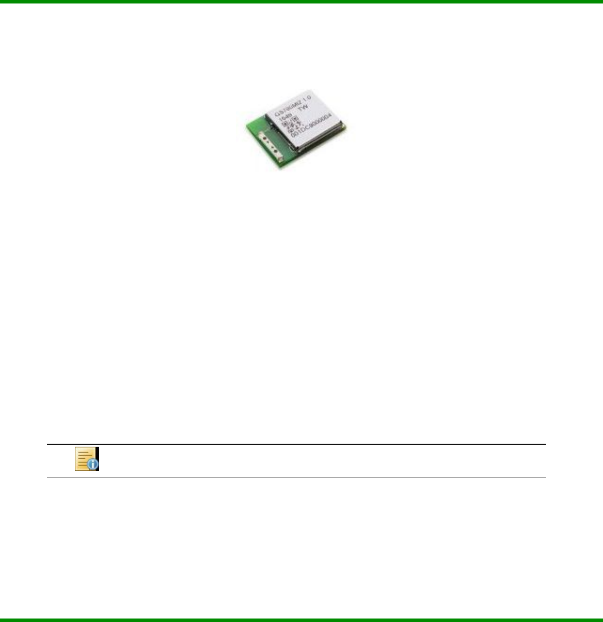
Gainspan GS780MIZ Bluetooth Smart Module User Manual GS780MIZ Module
Gainspan Corporation Bluetooth Smart Module GS780MIZ Module
Gainspan >
Users Manual

GS780MIZ Module
OEM / Integrator Installation Manual
Data Sheet
GS780M-DS-00001
GainSpan® 802.15 Bluetooth® BLE Module
Release 1.03, May 26, 2016
Copyright © 2016 GainSpan. All rights reserved.

GS780MIZ Module Data Sheet
Table of Contents
Introduction.......................................................................................................................................................... 3
Features.......................................................................................................................................................... 4
References..................................................................................................................................................... 4
Specifications................................................................................................................................................. 5
Pin Assignments................................................................................................................................................ 6
Device Pin-out............................................................................................................................................... 6
Module Pin Descriptions............................................................................................................................. 7
Port Functions.............................................................................................................................................. 10
Electrical Characteristics............................................................................................................................... 11
Recommended Operating Conditions................................................................................................... 11
Absolute Maximum Specifications [TBD]............................................................................................. 11
Digital I/O Pin Specifications [TBD]....................................................................................................... 11
RL78/G1D..................................................................................................................................................... 12
Packaging and Layout Guidelines.............................................................................................................. 13
Recommended PCB Footprint and Dimensions ............................................................................... 13
Surface Mount Assembly.......................................................................................................................... 16
Moisture Conditions................................................................................................................................... 18
GS780M-DS-00001 Page 2 Preliminary
Release 1.03 Confidential May 26, 2016
GS780MIZ Module Data Sheet
Introduction
The low-power GS780MIZ module adds low-power Bluetooth® low energy technology (BLE), version 4.2,
connectivity to devices intended for portable applications.
The module offers extended communication range in single-mode BLE operation with reduced power
consumption for extended battery life. You can operate the GS780MIZin either standalone mode with application
software running on the module, or connected to a microcontroller running the application software and
communicating through a UART or SPI interface. The module operates in the 2.4 to 2.485 GHz frequency range
using spread-spectrum, frequency-hopping, full-duplex modes, and will meet FCC/IC (US/Canada),
CE/ETSI(Europe), and TELEC(Japan) regulatory certification requirements.
The GS780MIZmodule reduces RF design and certification times to facilitate quick time-to-market. The small
form factor and adaptable RF technology, trading off sensitivity, interference and power, permit you to build
products customized to your application requirements. At the GS780MIZcore are,
•Renesas RL78/G1D
•program and data flash and SRAM memory
•Bluetooth low energy technology v4.2 single-mode master/slave RF with on-chip oscillator
•flexible MCU/RF power management modes
•real-time clock, watchdog and interval timers
•A/D converter
•3-wire serial I/O (CSI), UART, and I2C communication interfaces
NOTE:
The module is Bluetooth low energy technology v4.2-qualified by Bluetooth SIG but does not
support long data packets and the latest privacy encryption, which are optional features of the
standard.
GS780M-DS-00001 Page 3 Preliminary
Release 1.03 Confidential May 26, 2016

GS780MIZ Module Data Sheet
Features
16-bit RL78 CPU Core 32 MHz CPU with 1MB
address space.
A/D converter 8-channel, 8/10-bit
resolution
On-Chip RF
Transceiver
Bluetooth low energy
technology v4.2 with 2.4
GHz ISM band, GFSK
modulation, TDMA/TDD
frequency hopping.
I/O Interfaces • 2x 7/8-bit CSI/SPI
• 2x 7/8/9-BIT UART
• 2x I2C master
• 1x I2C multi-master
• GPIO: 23 ports
Program Flash Memory 256KB ROM, approx.
110KB stack
Power functions • Power-on reset
• Selectable low voltage
detector
Data Flash Memory 8KB Package Type, Pin
Count
30-pin
RAM 20KB, approx. 8KB stack Certifications and
Compliance
FCC, IC, TELEC, CE/ETSI
(planned)
DMA Controller 4 programmable channels,
8/16-bit
Standby function Reduced current: HALT,
STOP, SNOOZE modes.
Real-time clock 99-year calendar, alarm
and constant period
interrupt.
Low Power Technology Automatically optimizes
power consumption based
on range.
Extended-Function
Timers
Eight 16-bit independent
timers, with two high-
accuracy timers.
Eight 12-bit interval timers
with interrupt.
Safety Functions IEC60730- and IEC61508-
compliant:
• Flash memory CRC
• RAM parity error
• RAM guard
• SFR guard
• Invalid memory access
• Frequency detection
• A/D test
Watchdog timer Detect infinite program
loop.
References
•Renesas RL78/G1D microcontroller documentation
•Bluetooth SIG
GS780M-DS-00001 Page 4 Preliminary
Release 1.03 Confidential May 26, 2016

GS780MIZ Module Data Sheet
Specifications
Pin Count 30 pins
Package solder down module; edge pins
RF Output Power (typical) GS780MIZ: 0 dBm
Rx Sensitivity GS780MIZ: -91 dBm
RF
Operating Frequency 2.4 GHz
Protocol IEEE 802.15.1, Bluetooth low energy technology v4.2
Antenna Ceramic
Operating Temperature -40 to +85 C
Encryption AES128
Certifications and Compliance planned: FCC, IC, TELEC, CE/ETSI
Safety functions
WDT, TRAP instruction, Flash memory CRC, RAM parity error detection,
Invalid memory access detection, Frequency detection, RAM and SFR guard,
A/DC test
MCU Core Renesas RL78, 16-bit
Frequency 32 MHz
Memory
Internal Flash 256KB program flash (approximately 110KB used for stack)
8KB data flash
RAM 20KB (8KB approximately used for stack)
External interrupt 3 channels
DMA 4 channels
I/O Interfaces SPI, UART, simple I2C, multi-master I2C, GPIO, PWM, 10-bit A/D
Host Connections SPI, UART
Timers 8 16-bit channels
4 channel PWM output, 7 channel multi PWM output
Real-time clock 1 channel
Outline Dimensions GS780MIZ: 12.5mm x 17mm x 2.2mm
Operating Voltage 1.8-3.6V
GS780M-DS-00001 Page 5 Preliminary
Release 1.03 Confidential May 26, 2016
GS780MIZ Module Data Sheet
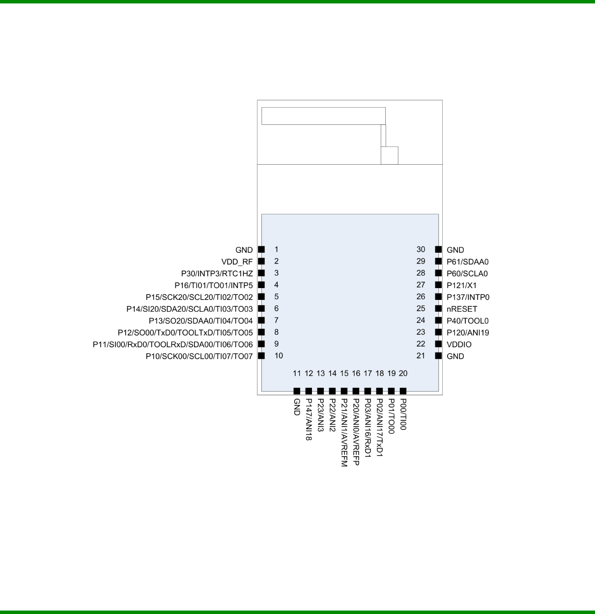
Pin Assignments
Device Pin-out
GS780M-DS-00001 Page 6 Preliminary
Release 1.03 Confidential May 26, 2016

GS780MIZ Module Data Sheet
Module Pin Descriptions
Pin no.
Pin name
Port
On Reset
Description
1
GND
̶
̶
Ground
2
VDD_RF
̶
̶
Supply for RF
3
P30
3 Input port
I/O
INTP3
External Interupt Input 3
RTC1HZ
Real-time clock: correction clock (1 Hz) output
4
P16
1 Input port
I/O
TI01
External count clock/capture 01
TO01
Timer Output 01
INTP5
External Interrupt Input 5
5
P15
I/O
SCK20
Clock I/O of SPI CSI20
SCL20
Clock Output SPI CSI20
TI02
External count clock/capture 02
TO02
Timer Output 02
6
P14
I/O
SI20
Data Input SPI CSI20
SDA20
Data I/O I2C20
SCLA0
Data Output I2CA0
TI03
External count clock/capture 03
TO03
Timer Output 03
7
P13
I/O
SO20
Data Output SPI CSI20
DSAA0
Data I/O I2CA0
TI04
External count clock/capture 04
TO04
Timer Output 04
8
P12
I/O
SO00
Data Output SPI CSI00
TxD0
Data Output UART0
TOOLTxD
Output UART Flash Memory Programming
TI05
External count clock/capture 05
TO05
Timer Output 05
GS780M-DS-00001 Page 7 Preliminary
Release 1.03 Confidential May 26, 2016

GS780MIZ Module Data Sheet
Pin no.
Pin name
Port
On Reset
Description
9
P11
I/O
SI00
Data Input SPI CSI00
RxD0
Data Input UART0
TOOLRxD
Input UART Flash Memory Programming
SDA00
Data I/O IIC00
TI06
External count clock/capture 06
TO06
Timer Output 06
10
P10
I/O
SCK00
Clock I/O of SPI CSI00
SCL00
Clock Output SPI CSI00
TI07
External count clock/capture 07
TO07
Timer Output 07
11
GND
̶
̶
Ground
12
P147
14 Analog
input port
I/O
ANI18
A/D converter analog input
13
P23
2Analog
input port
I/O
ANI3
A/D converter analog input
14
P22
I/O
ANI2
A/D converter analog input
15
P21
I/O
ANI1
A/D converter analog input
AVREFM
Analog Reference Minus
16
P20
I/O
ANI0
A/D converter analog input
AVREFP
Analog Reference Plus
17
P03
0
Analog
input port
I/O
ANI16
A/D converter analog input
RxD1
Data Input UART1
18
P02
I/O
ANI17
A/D converter analog input
TxD1
Data Output UART1
19
P01
Input port
I/O
TO00
Timer Output 00
20
P00
I/O
TI00
External count clock/capture 00
21
GND
̶
̶
Ground
GS780M-DS-00001 Page 8 Preliminary
Release 1.03 Confidential May 26, 2016

GS780MIZ Module Data Sheet
Pin no.
Pin name
Port
On Reset
Description
22
VDDIO
̶
̶
Supply for Digital IO
23
P120
12 Analog
input port
I/O
ANI19
A/D converter analog input
24
P40
4 Input port
I/O
TOOL0
Programming Pin
25
nRESET
̶
̶
Active-low system reset input
26
P137
13 Input port
Input
INTP0
External Interrupt Input 0
27
P121
12 Input port
I/O
X1
General Purpose Input
28
P60
6 Input port
I/O
SCLA0
Data Output I2CA0
29
P61
I/O
SDAA0
Data Input I2CA0
30
GND
̶
̶
Ground
GS780M-DS-00001 Page 9 Preliminary
Release 1.03 Confidential May 26, 2016

GS780MIZ Module Data Sheet
Port Functions
Port Function
0
4-bit I/O port.
Input/output can be specified in 1-bit units.
Use of an on-chip pull-up resistor can be specified by a
software setting at input port.
Input of P01 and P03 can be set to TTL input buffer.
Output of P00, P02, and P03 can be set to N-ch open-
drain output (VDD tolerance).
P02 and P03 can be set to analog input.
1
7-bit I/O port.
Input/output can be specified in 1-bit units.
Use of an on-chip pull-up resistor can be specified by a
software setting at input port.
Input of P10, P11, and P13 to P16 can be set to TTL
input buffer.
Output of P10 to P15 can be set to N-ch open drain
output (VDD tolerance).
2
4-bit I/O port.
Input/output can be specified in 1-bit units.
Can be set to analog input.
3
Input/output can be specified in 1-bit units.
Use of an on-chip pull-up resistor can be specified by a
software setting at input port.
4
Input/output can be specified in 1-bit units.
Use of an on-chip pull-up resistor can be specified by a
software setting at input port.
6
2-bit I/O port.
Input/output can be specified in 1-bit units.
N-ch open-drain output (6V tolerance).
12
For only P120, input/output can be specified.
For only P120, use of an on-chip pull-up resistor
can be specified by a software setting at input port.
P120 can be set to analog input.
P121 is input-only.
13 P137 1-bit input-only port.
14
2-bit I/O port.
Input/output can be specified in 1-bit units.
Use of an on-chip pull-up resistor can be specified by a
software setting at input port.
P147 can be set to analog input.
GS780M-DS-00001 Page 10 Preliminary
Release 1.03 Confidential May 26, 2016

GS780MIZ Module Data Sheet
Electrical Characteristics
Recommended Operating Conditions
Characteristic Value
Supply voltage
Maximum voltage rating
Power consumption
Maximum 3.3V output current draw
Absolute Maximum Specifications [TBD]
Characteristic Value
Digital I/O Pin Specifications [TBD]
Characteristic Value
[TBD: POWER CONSUMPTION SPEC, RADIO CHARACTERISTICS SPEC]
GS780M-DS-00001 Page 11 Preliminary
Release 1.03 Confidential May 26, 2016
GS780MIZ Module Data Sheet
RL78/G1D
Refer to Renesas RL78/G1D Datasheet for details about the electrical characteristics listed in the following table.
Section Characteristic/Title Renesas Datasheet
Page Number
2.1 Absolute Maximum Ratings 11
2.2 Operating Voltage 13
2.3 Oscillator Characteristics 14
2.4 DC Characteristics 15
2.5 Current Consumption 19
2.6 AC Characteristics 25
2.7 Peripheral Functions Characteristics 29
2.7.1 Serial array unit 29
2.7.2 Serial interface IICA 54
2.8 Analog Characteristics 58
2.9 RF Transceiver Characteristics 65
2.10 RAM Data Retention Characteristics 72
2.11 Flash Memory Programming Characteristics 72
2.12 Special Flash Memory Programming Communication (UART) 72
2.13 Timing of Entry to Flash Memory Programming Modes 73
NOTE: Document section, title, and page number refer to Renesas document R01DS0258EJ0110
Rev.1.10, dated Sep 25, 2015.
GS780M-DS-00001 Page 12 Preliminary
Release 1.03 Confidential May 26, 2016
GS780MIZ Module Data Sheet
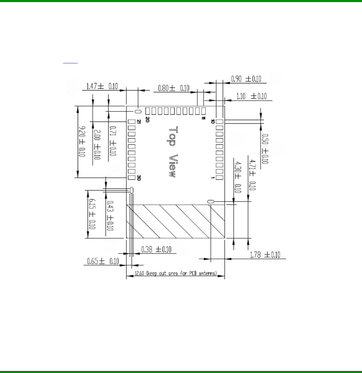
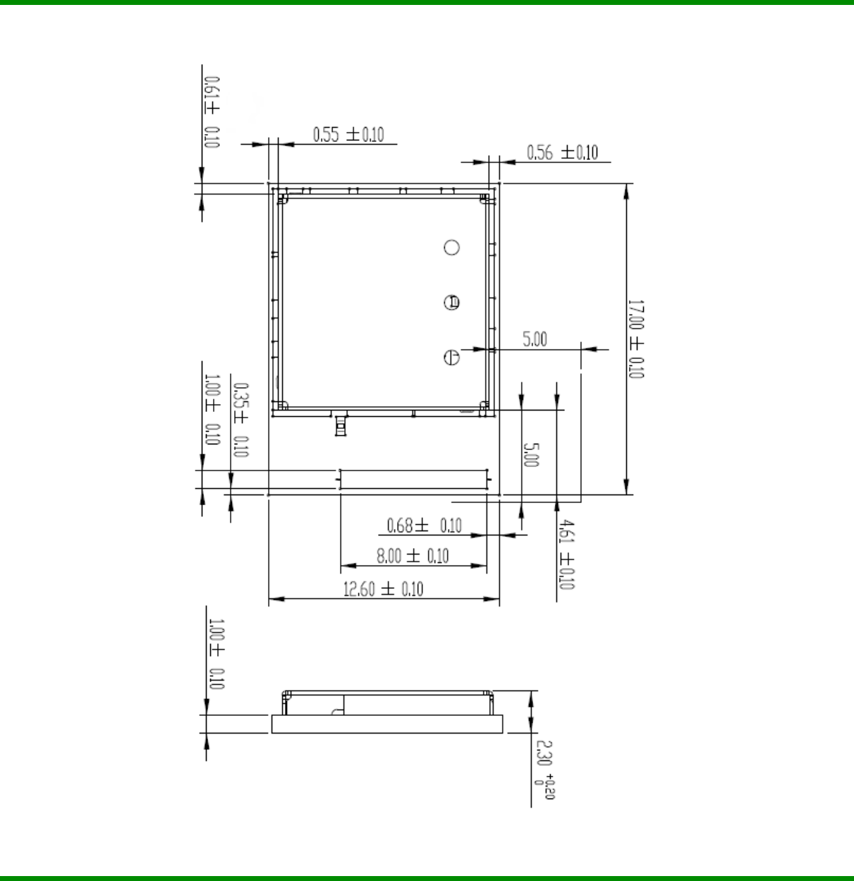
Packaging and Layout Guidelines
Recommended PCB Footprint and Dimensions
The following figures show the module dimensions and recommended footprint. The first figure shows the
recommended PCB antenna keep-out area. The second figure shows the GS780MIZ package dimensions.
(Refer to the notes following the figures for additional mechanical recommendations.)
GS780M-DS-00001 Page 13 Preliminary
Release 1.03 Confidential May 26, 2016
GS780MIZ Module Data Sheet
GS780M-DS-00001 Page 14 Preliminary
Release 1.03 Confidential May 26, 2016

GS780MIZ Module Data Sheet
NOTES:
1. All Dimensions are in millimeters (mm).
2. For Boards using Ceramic Antenna, we recommend:
◦Have Only Air on BOTH sides of antenna.
◦Hang Antenna over edge of base board (best);
◦Or, cut notch in base board under antenna area:
◦5mm beyond module edge on each side is good.
◦full module width is minimum.
◦No metal or FR4 encircling antenna area.
◦Antenna at edge of base board, not interior of base board.
◦Nothing conductive near antenna (e.g. battery, display, wire).
3. Module solder pads on footprint should be the same size as the pads on the module. The
three RF shield mounting holes have exposed metal. These areas must not have metal on the
customer board.
4. For best RF performance, we recommend:
◦Using power (PWR) or GND planes from module back to power supply.
◦Isolating PWR/GND from high frequency or high current components. For example, a
notch in GND plane to isolate from host uC.
◦Using at least three vias when either power or GND changes layers. This applies
particularly at the module GND pins and at the VDD_RF pin.
◦Providing a 10 uF capacitor at the VDD_RF pin and using three vias both sides of the
capacitor.
◦Keep high speed signals away from RF areas of module.
5. For area under module, other than the antenna area, we recommend two options:
◦No metal of any kind under module “not on any layer.”
◦Having full GND plane under module (layer 1 or layer 2) with no “HOT” vias under
module (over 100KHz), and may route signals below GND plane. Also, no metal traces
are to be present in the circle, around shield and alignment holes. This option is best for
2-layer boards. If GND is on layer 1, use thermal relief pads for the GND pins of the
module footprint.
6. If any metal is present on layer 1, extra thick solder mask under the module is required.
7. In performing SMT or manual soldering of the module to the base board, first align the row
of pins from #11 through #20 onto the base board, then match the other two rows.
In addition to the guidelines, note the following suggestions:
1. External bypass capacitors for all module supplies should be as close as possible to the
module pins.
2. Never place the antenna very close to metallic objects.
3. External monopole antennas need a reasonable ground plane area for antenna efficiency.
4. Do not use a metallic or metalized plastic for the end product enclosure when using on-
board antenna.
5. If the module is enclosed in a plastic case, have reasonable clearance from plastic case to on-
board antenna.
GS780M-DS-00001 Page 15 Preliminary
Release 1.03 Confidential May 26, 2016
GS780MIZ Module Data Sheet
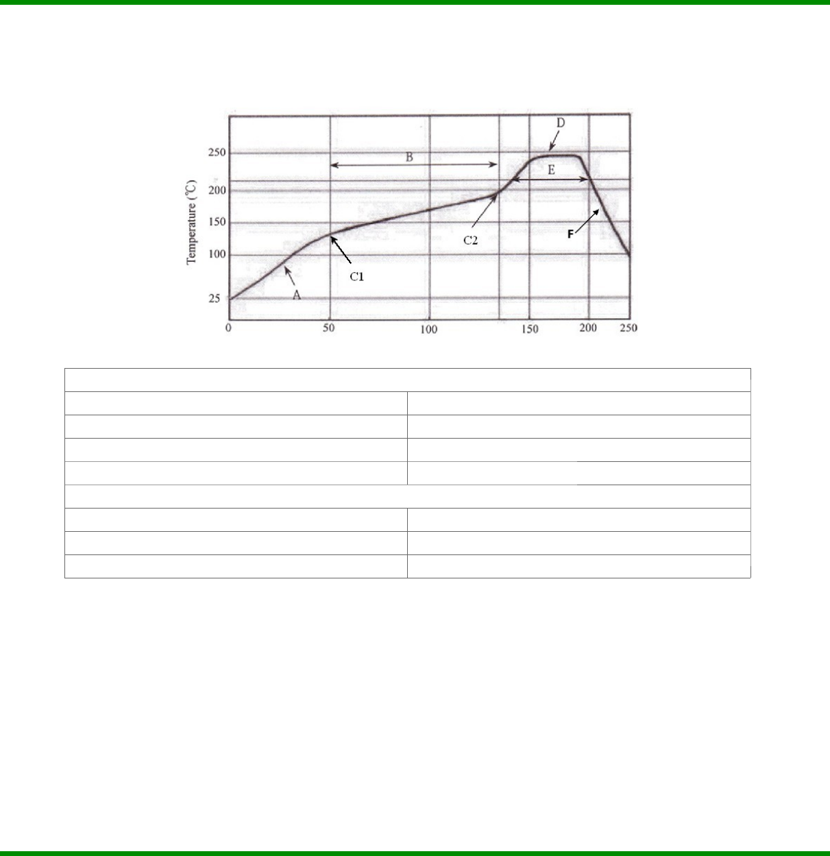
Surface Mount Assembly
The figure shows the reflow profile, and the recommended reflow parameters are summarized in the following
table.
Preheat
Temperature Ramp up rate for (A)2 1.5~3.5 oC/s
Pre-heat time (B)3 80 to 130 seconds
Pre-heat starting temperature (C1) 125 to 135 oC
Pre-heat ending temperature (C2) 180 to 200 oC
Heating
Peak Temperature range (D) 240 to 250 oC
Melting time4 that is the time over 220 oC (E) 50 to 75 seconds
Cool Down Ramp (F) >2 oC/s
GS780M-DS-00001 Page 16 Preliminary
Release 1.03 Confidential May 26, 2016

GS780MIZ Module Data Sheet
NOTES:
1. Perform adequate test in advance as the reflow temperature profile varies according to the
conditions of the parts and boards, and the specifications of the reflow furnace.
2. Max number of reflow supported is two.
3. Temperature uniformity inside the IR reflow oven must be tightly controlled and multiple
thermocouples should be used. The locations should also include multiple points INSIDE the
module RF shield. The temperature profile of all thermocouples must meet the requirements
of the above table.
4. Pay close attention to “Melting Time over 220oC”. Sufficient time is needed to completely
melt all solder.
5. Be careful about rapid temperature rise in preheat zone because it can cause excessive
slumping of the solder paste.
6. If the preheat is insufficient, large solder balls tend to be generated. Conversely, if
performed excessively, fine balls and large balls will generate in clusters at a time.
7. If the temperature is too low, non-melting tends to be caused in the area with large heat
capacity after reflow.
8. Be careful about sudden rise in temperature because it may increase the slump of solder
paste.
9. Be careful about slow cooling because it can cause the positional shift of parts and a decline
in joining at times.
10. A no clean flux should be used during the SMT process.
GS780M-DS-00001 Page 17 Preliminary
Release 1.03 Confidential May 26, 2016
GS780MIZ Module Data Sheet
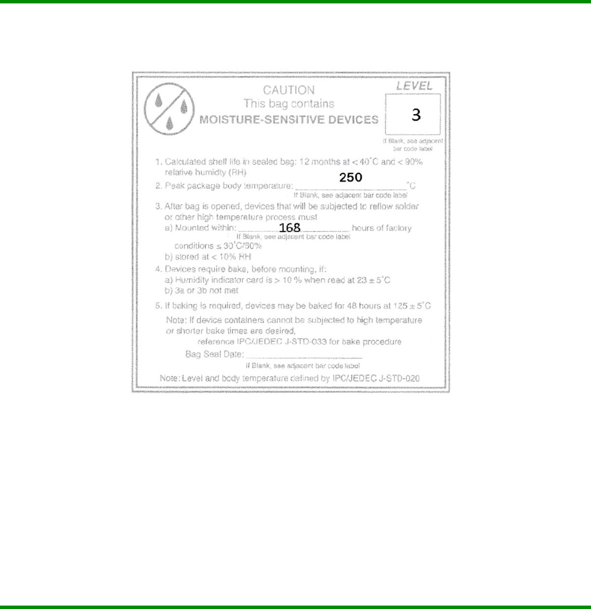
Moisture Conditions
The modules are shipped in sealed trays with the following conditions indicated on the label:
GS780M-DS-00001 Page 18 Preliminary
Release 1.03 Confidential May 26, 2016
FCC Statement:
Federal Communication Commission Interference Statement
This equipment has been tested and found to comply with the limits for a Class B digital device,
pursuant to Part 15 of the FCC Rules. These limits are designed to provide reasonable protection
against harmful interference in a residential installation. This equipment generates, uses and can
radiate radio frequency energy and, if not installed and used in accordance with the instructions, may
cause harmful interference to radio communications. However, there is no guarantee that interference
will not occur in a particular installation. If this equipment does cause harmful interference to radio or
television reception, which can be determined by turning the equipment off and on, the user is
encouraged to try to correct the interference by one of the following measures:
●Reorient or relocate the receiving antenna.
●Increase the separation between the equipment and receiver.
●Connect the equipment into an outlet on a circuit different from that to which the receiver is
connected.
●Consult the dealer or an experienced radio/TV technician for help.
FCC Caution: Any changes or modifications not expressly approved by the party responsible for
compliance could void the user’s authority to operate this equipment.
This device complies with Part 15 of the FCC Rules. Operation is subject to the following two
conditions: (1) This device may not cause harmful interference, and (2) this device must accept any
interference received, including interference that may cause undesired operation.
IMPORTANT NOTE:
FCC Radiation Exposure Statement:
This equipment complies with FCC radiation exposure limits set forth for an uncontrolled environment.
This equipment should be installed and operated with minimum distance 20cm between the radiator
& your body.
The module is limited to OEM installation only.
OEM Integrators shall be responsible for ensuring that the end-user has no manual / instructions to
remove or install the module.
IMPORTANT NOTE:
This module is intended for OEM integrator. The OEM integrator is responsible for the compliance to
all the rules that apply to the product into which this certified RF module is integrated.
Additional testing and certification may be necessary when multiple modules are used.
USERS MANUAL OF THE END PRODUCT:
In the users manual of the end product, the end user has to be informed to keep at least 20cm
separation with the antenna while this end product is installed and operated. The end user has to be
informed that the FCC radio-frequency exposure guidelines for an uncontrolled environment can be
satisfied.
The end user has to also be informed that any changes or modifications not expressly approved by
the manufacturer could void the user's authority to operate this equipment.
If the labelling area is small than the palm of the hand, then additional FCC part 15.19 statement is
required to be available in the users manual: This device complies with Part 15 of FCC rules.
Operation is subject to the following two conditions: (1) this device may not cause harmful interference
and (2) this device must accept any interference received, including interference that may cause
undesired operation.
LABEL OF THE END PRODUCT:
The final end product must be labeled in a visible area with the following " Contains TX FCC ID:
YOPGS780MIZ ".
If the labelling area is larger than the palm of the hand, then the following FCC part 15.19 statement
has to also be available on the label: This device complies with Part 15 of FCC rules. Operation is
subject to the following two conditions: (1) this device may not cause harmful interference and (2) this
device must accept any interference received, including interference that may cause undesired
operation.
The installation is limited to mobile installation only.
A separate approval is required for all other operating modes not covered in this filing.
IC Statement:
This device complies with Industry Canada license-exempt RSS standard(s). Operation is subject to
the following two conditions: (1) this device may not cause interference, and (2) this device must
accept any interference, including interference that may cause undesired operation of the device.
Le présent appareil est conforme aux CNR d'Industrie Canada applicables aux appareils radio exempts de licence.
L'exploitation est autorisée aux deux conditions suivantes : (1) l'appareil ne doit pas produire de brouillage, et (2)
l'utilisateur de l'appareil doit accepter tout brouillage radioélectrique subi, même si le brouillage est susceptible d'en
compromettre le fonctionnement.
IMPORTANT NOTE:
IC Radiation Exposure Statement:
This equipment complies with IC RSS-102 radiation exposure limits set forth for an uncontrolled
environment. This equipment should be installed and operated with minimum distance 20cm between
the radiator & your body.
Cet équipement est conforme aux limites d'exposition aux rayonnements IC établies pour un environnement non contrôlé.
Cet équipement doit être installé et utilisé avec un minimum de 20 cm de distance entre la source de rayonnement et votre
corps.
IMPORTANT NOTE:
This module is intended for OEM integrator. The OEM integrator is responsible for the compliance to
all the rules that apply to the product into which this certified RF module is integrated.
Additional testing and certification may be necessary when multiple modules are used.
Any changes or modifications not expressly approved by the manufacturer could void the user's
authority to operate this equipment.
USERS MANUAL OF THE END PRODUCT:
In the users manual of the end product, the end user has to be informed to keep at least 20cm
separation with the antenna while this end product is installed and operated. The end user has to be
informed that the IC radio-frequency exposure guidelines for an uncontrolled environment can be
satisfied.
The end user has to also be informed that any changes or modifications not expressly approved by
the manufacturer could void the user's authority to operate this equipment. Operation is subject to the
following two conditions: (1) this device may not cause harmful interference and (2) this device must
accept any interference received, including interference that may cause undesired operation.
LABEL OF THE END PRODUCT:
The final end product must be labeled in a visible area with the following " Contains IC:
9154A-GS780MIZ ".
The Host Model Number (HMN) must be indicated at any location on the exterior of the end product or
product packaging or product literature which shall be available with the end product or online.