Galaxy Tracking Systems VTRAKH450 UHF-FM VehicleTracking Unit User Manual Cover
Galaxy Tracking Systems L.L.C. UHF-FM VehicleTracking Unit Cover
Contents
- 1. Users Manual1
- 2. Users Manual2
- 3. Service Manual
Service Manual

HIGH SPECIFICATION DATA TRANSCEIVER
PART NO. 242-3474-XX0
Second Printing
August 1998
Part No. 001-3474-002 8-98 Printed in U.S.A.


HIGH SPECIFICATION DATA TRANSCEIVER
PART NO. 242-3474-XX0
Copyright 1998 by the Johnson Data Telemetry Corporation.
The Johnson Data Telemetry Corporation designs and manufactures radios and radio modems to serve a wide variety of data
communication needs. The Johnson Data Telemetry Corporation produces equipment for the fixed data market including
SCADA systems for utilities, petrochemical, waste and fresh water management markets and RF boards for OEM applications
in the Radio Frequency Data Capture market.
DATA TELEMETRY PRODUCT WARRANTY
The manufacturer's warranty statement for this product is available from your product supplier or from the Johnson Data
Telemetry Corporation, 299 Johnson Avenue, Box 1733, Waseca, MN 56093-0833. Phone (507) 835-8819.
WARNING
This device complies with Part 15 of the FCC rules. Operation is subject to the condition that this device does not cause
harmful interference. In addition, changes or modification to this equipment not expressly approved by Johnson Data
Telemetry Corporation could void the user's authority to operate this equipment (FCC rules, 47CFR Part 15.19).
DO NOT allow the antenna to come close to or touch, the eyes, face, or any exposed body parts while the radio is transmitting.
DO NOT operate the radio near electrical blasting caps or in an explosive atmosphere.
DO NOT operate the radio unless all the radio frequency connectors are secure and any open connectors are properly
terminated.
DO NOT allow children to operate transmitter equipped radio equipment.
SAFETY INFORMATION
Proper operation of this radio will result in user exposure below the Occupational Safety and Health Act and Federal
Communication Commission limits.
The information in this document is subject to change without notice.
is a trademark of the Johnson Data Telemetry Corporation.


i
TABLE OF CONTENTS
1GENERAL INFORMATION
1.1 SCOPE OF MANUAL . . . . . . . . . . . . . . . . . . . . . . . . . . . . . . . . . . . . . . . . . . . . . . . . . . . . . . . . . . . . . . . . . . . . . . . . .1-1
1.2 EQUIPMENT DESCRIPTION. . . . . . . . . . . . . . . . . . . . . . . . . . . . . . . . . . . . . . . . . . . . . . . . . . . . . . . . . . . . . . . . . .1-1
GENERAL . . . . . . . . . . . . . . . . . . . . . . . . . . . . . . . . . . . . . . . . . . . . . . . . . . . . . . . . . . . . . . . . . . . . . . . . . . . . . . . . . . 1-1
DM3474 SYNTHESIZER PROGRAMMING . . . . . . . . . . . . . . . . . . . . . . . . . . . . . . . . . . . . . . . . . . . . . . . . . . . . . . 1-1
1.3 TRANSCEIVER IDENTIFICATION . . . . . . . . . . . . . . . . . . . . . . . . . . . . . . . . . . . . . . . . . . . . . . . . . . . . . . . . . . . .1-1
1.4 PART NUMBER BREAKDOWN . . . . . . . . . . . . . . . . . . . . . . . . . . . . . . . . . . . . . . . . . . . . . . . . . . . . . . . . . . . . . . .1-2
1.5 ACCESSORIES . . . . . . . . . . . . . . . . . . . . . . . . . . . . . . . . . . . . . . . . . . . . . . . . . . . . . . . . . . . . . . . . . . . . . . . . . . . . . .1-2
1.6 FACTORY CUSTOMER SERVICE . . . . . . . . . . . . . . . . . . . . . . . . . . . . . . . . . . . . . . . . . . . . . . . . . . . . . . . . . . . . .1-2
1.7 PRODUCT WARRANTY . . . . . . . . . . . . . . . . . . . . . . . . . . . . . . . . . . . . . . . . . . . . . . . . . . . . . . . . . . . . . . . . . . . . . .1-3
1.8 REPLACEMENT PARTS. . . . . . . . . . . . . . . . . . . . . . . . . . . . . . . . . . . . . . . . . . . . . . . . . . . . . . . . . . . . . . . . . . . . . .1-3
1.9 IF A PROBLEM ARISES . . . . . . . . . . . . . . . . . . . . . . . . . . . . . . . . . . . . . . . . . . . . . . . . . . . . . . . . . . . . . . . . . . . . . .1-4
FACTORY REPAIR . . . . . . . . . . . . . . . . . . . . . . . . . . . . . . . . . . . . . . . . . . . . . . . . . . . . . . . . . . . . . . . . . . . . . . . . . . .1-4
GENERAL SPECIFICATIONS . . . . . . . . . . . . . . . . . . . . . . . . . . . . . . . . . . . . . . . . . . . . . . . . . . . . . . . . . . . . . . . . .1-5
2INSTALLATION
2.1 PRE-INSTALLATION CHECKS . . . . . . . . . . . . . . . . . . . . . . . . . . . . . . . . . . . . . . . . . . . . . . . . . . . . . . . . . . . . . . .2-1
2.2 INTERFACING WITH DATA EQUIPMENT . . . . . . . . . . . . . . . . . . . . . . . . . . . . . . . . . . . . . . . . . . . . . . . . . . . . .2-1
DM3474 ONLY . . . . . . . . . . . . . . . . . . . . . . . . . . . . . . . . . . . . . . . . . . . . . . . . . . . . . . . . . . . . . . . . . . . . . . . . . . . . . . .2-1
3PROGRAMMING
3.1 INTRODUCTION . . . . . . . . . . . . . . . . . . . . . . . . . . . . . . . . . . . . . . . . . . . . . . . . . . . . . . . . . . . . . . . . . . . . . . . . . . . .3-1
3.2 DM3474 SYNTHESIZER DATA PROTOCOL . . . . . . . . . . . . . . . . . . . . . . . . . . . . . . . . . . . . . . . . . . . . . . . . . . . .3-1
D-WORD . . . . . . . . . . . . . . . . . . . . . . . . . . . . . . . . . . . . . . . . . . . . . . . . . . . . . . . . . . . . . . . . . . . . . . . . . . . . . . . . . . . .3-1
B-WORD . . . . . . . . . . . . . . . . . . . . . . . . . . . . . . . . . . . . . . . . . . . . . . . . . . . . . . . . . . . . . . . . . . . . . . . . . . . . . . . . . . . .3-2
A-WORD . . . . . . . . . . . . . . . . . . . . . . . . . . . . . . . . . . . . . . . . . . . . . . . . . . . . . . . . . . . . . . . . . . . . . . . . . . . . . . . . . . . .3-2
3.3 RECEIVE TO TRANSMIT SEQUENCE . . . . . . . . . . . . . . . . . . . . . . . . . . . . . . . . . . . . . . . . . . . . . . . . . . . . . . . . .3-6
3.4 TRANSMIT TO RECEIVE SEQUENCE . . . . . . . . . . . . . . . . . . . . . . . . . . . . . . . . . . . . . . . . . . . . . . . . . . . . . . . . .3-7
4CIRCUIT DESCRIPTION
4.1 GENERAL . . . . . . . . . . . . . . . . . . . . . . . . . . . . . . . . . . . . . . . . . . . . . . . . . . . . . . . . . . . . . . . . . . . . . . . . . . . . . . . . . .4-1
INTRODUCTION . . . . . . . . . . . . . . . . . . . . . . . . . . . . . . . . . . . . . . . . . . . . . . . . . . . . . . . . . . . . . . . . . . . . . . . . . . . . .4-1
SYNTHESIZER . . . . . . . . . . . . . . . . . . . . . . . . . . . . . . . . . . . . . . . . . . . . . . . . . . . . . . . . . . . . . . . . . . . . . . . . . . . . . . .4-1
RECEIVER. . . . . . . . . . . . . . . . . . . . . . . . . . . . . . . . . . . . . . . . . . . . . . . . . . . . . . . . . . . . . . . . . . . . . . . . . . . . . . . . . . .4-1
TRANSMITTER . . . . . . . . . . . . . . . . . . . . . . . . . . . . . . . . . . . . . . . . . . . . . . . . . . . . . . . . . . . . . . . . . . . . . . . . . . . . . .4-2
4.2 SYNTHESIZER . . . . . . . . . . . . . . . . . . . . . . . . . . . . . . . . . . . . . . . . . . . . . . . . . . . . . . . . . . . . . . . . . . . . . . . . . . . . . .4-2
INTRODUCTION . . . . . . . . . . . . . . . . . . . . . . . . . . . . . . . . . . . . . . . . . . . . . . . . . . . . . . . . . . . . . . . . . . . . . . . . . . . . .4-2
VOLTAGE-CONTROLLED OSCILLATOR . . . . . . . . . . . . . . . . . . . . . . . . . . . . . . . . . . . . . . . . . . . . . . . . . . . . . . . .4-5
VCO AND REFERENCE OSCILLATOR MODULATION . . . . . . . . . . . . . . . . . . . . . . . . . . . . . . . . . . . . . . . . . . . .4-6
CASCODE AMPLIFIERS (Q851/Q852). . . . . . . . . . . . . . . . . . . . . . . . . . . . . . . . . . . . . . . . . . . . . . . . . . . . . . . . . . . .4-6
AMPLIFIER (Q853) . . . . . . . . . . . . . . . . . . . . . . . . . . . . . . . . . . . . . . . . . . . . . . . . . . . . . . . . . . . . . . . . . . . . . . . . . . .4-6
VOLTAGE FILTER (Q832) . . . . . . . . . . . . . . . . . . . . . . . . . . . . . . . . . . . . . . . . . . . . . . . . . . . . . . . . . . . . . . . . . . . . .4-6
VCO FREQUENCY SHIFT (Q831) . . . . . . . . . . . . . . . . . . . . . . . . . . . . . . . . . . . . . . . . . . . . . . . . . . . . . . . . . . . . . . .4-6
SYNTHESIZER INTEGRATED CIRCUIT (U801) . . . . . . . . . . . . . . . . . . . . . . . . . . . . . . . . . . . . . . . . . . . . . . . . . . .4-7
LOCK DETECT. . . . . . . . . . . . . . . . . . . . . . . . . . . . . . . . . . . . . . . . . . . . . . . . . . . . . . . . . . . . . . . . . . . . . . . . . . . . . . .4-7

TABLE OF CONTENTS
ii
4.3 RECEIVER CIRCUIT DESCRIPTION . . . . . . . . . . . . . . . . . . . . . . . . . . . . . . . . . . . . . . . . . . . . . . . . . . . . . . . . . 4-8
HELICAL FILTER (Z201), RF AMPLIFIER (Q201) . . . . . . . . . . . . . . . . . . . . . . . . . . . . . . . . . . . . . . . . . . . . . . . . . 4-8
MIXER (U221), FIRST LO AMPLIFIER (Q301) . . . . . . . . . . . . . . . . . . . . . . . . . . . . . . . . . . . . . . . . . . . . . . . . . . . . 4-8
AMPLIFIER (Q222), CRYSTAL FILTER (Z221/Z222), IF AMP (Q221). . . . . . . . . . . . . . . . . . . . . . . . . . . . . . . . . 4-8
SECOND LO AMP/TRIPLER (Q401), SECOND IF FILTER (Q901). . . . . . . . . . . . . . . . . . . . . . . . . . . . . . . . . . . . 4-9
SECOND MIXER/DETECTOR (U241) . . . . . . . . . . . . . . . . . . . . . . . . . . . . . . . . . . . . . . . . . . . . . . . . . . . . . . . . . . . 4-9
4.4 TRANSMITTER CIRCUIT DESCRIPTION . . . . . . . . . . . . . . . . . . . . . . . . . . . . . . . . . . . . . . . . . . . . . . . . . . . . 4-10
BUFFER (Q851). . . . . . . . . . . . . . . . . . . . . . . . . . . . . . . . . . . . . . . . . . . . . . . . . . . . . . . . . . . . . . . . . . . . . . . . . . . . . 4-10
PRE-DRIVER (Q501), DRIVER (Q521). . . . . . . . . . . . . . . . . . . . . . . . . . . . . . . . . . . . . . . . . . . . . . . . . . . . . . . . . . 4-11
-5V POWER CONTROL SUPPLY . . . . . . . . . . . . . . . . . . . . . . . . . . . . . . . . . . . . . . . . . . . . . . . . . . . . . . . . . . . . . . 4-11
FINAL (Q541), POWER CONTROL (U542) . . . . . . . . . . . . . . . . . . . . . . . . . . . . . . . . . . . . . . . . . . . . . . . . . . . . . . 4-11
ANTENNA SWITCH (CR561, CR562). . . . . . . . . . . . . . . . . . . . . . . . . . . . . . . . . . . . . . . . . . . . . . . . . . . . . . . . . . . 4-11
5SERVICING
5.1 GENERAL. . . . . . . . . . . . . . . . . . . . . . . . . . . . . . . . . . . . . . . . . . . . . . . . . . . . . . . . . . . . . . . . . . . . . . . . . . . . . . . . . . 5-1
PERIODIC CHECKS . . . . . . . . . . . . . . . . . . . . . . . . . . . . . . . . . . . . . . . . . . . . . . . . . . . . . . . . . . . . . . . . . . . . . . . . . . 5-1
SURFACE-MOUNTED COMPONENTS . . . . . . . . . . . . . . . . . . . . . . . . . . . . . . . . . . . . . . . . . . . . . . . . . . . . . . . . . . 5-1
SCHEMATIC DIAGRAMS AND COMPONENT LAYOUTS . . . . . . . . . . . . . . . . . . . . . . . . . . . . . . . . . . . . . . . . . 5-1
REPLACEMENT PARTS LIST. . . . . . . . . . . . . . . . . . . . . . . . . . . . . . . . . . . . . . . . . . . . . . . . . . . . . . . . . . . . . . . . . . 5-1
TCXO MODULE NOT SERVICEABLE . . . . . . . . . . . . . . . . . . . . . . . . . . . . . . . . . . . . . . . . . . . . . . . . . . . . . . . . . . 5-1
5.2 SYNTHESIZER SERVICING . . . . . . . . . . . . . . . . . . . . . . . . . . . . . . . . . . . . . . . . . . . . . . . . . . . . . . . . . . . . . . . . . 5-1
INTRODUCTION . . . . . . . . . . . . . . . . . . . . . . . . . . . . . . . . . . . . . . . . . . . . . . . . . . . . . . . . . . . . . . . . . . . . . . . . . . . . 5-1
REFERENCE OSCILLATOR . . . . . . . . . . . . . . . . . . . . . . . . . . . . . . . . . . . . . . . . . . . . . . . . . . . . . . . . . . . . . . . . . . . 5-2
VCO . . . . . . . . . . . . . . . . . . . . . . . . . . . . . . . . . . . . . . . . . . . . . . . . . . . . . . . . . . . . . . . . . . . . . . . . . . . . . . . . . . . . . . . 5-2
SYNTHESIZER (U801) . . . . . . . . . . . . . . . . . . . . . . . . . . . . . . . . . . . . . . . . . . . . . . . . . . . . . . . . . . . . . . . . . . . . . . . . 5-2
5.3 RECEIVER SERVICING . . . . . . . . . . . . . . . . . . . . . . . . . . . . . . . . . . . . . . . . . . . . . . . . . . . . . . . . . . . . . . . . . . . . . 5-3
SUPPLY VOLTAGES AND CURRENT . . . . . . . . . . . . . . . . . . . . . . . . . . . . . . . . . . . . . . . . . . . . . . . . . . . . . . . . . . 5-3
MIXER/DETECTOR (U201). . . . . . . . . . . . . . . . . . . . . . . . . . . . . . . . . . . . . . . . . . . . . . . . . . . . . . . . . . . . . . . . . . . . 5-3
RF AMPLIFIER (Q201) AND FIRST MIXER (Q221). . . . . . . . . . . . . . . . . . . . . . . . . . . . . . . . . . . . . . . . . . . . . . . . 5-4
RF AND IF AMPLIFIERS, FIRST MIXER . . . . . . . . . . . . . . . . . . . . . . . . . . . . . . . . . . . . . . . . . . . . . . . . . . . . . . . . 5-4
5.4 TRANSMITTER SERVICING . . . . . . . . . . . . . . . . . . . . . . . . . . . . . . . . . . . . . . . . . . . . . . . . . . . . . . . . . . . . . . . . . 5-4
SUPPLY VOLTAGES AND CURRENT . . . . . . . . . . . . . . . . . . . . . . . . . . . . . . . . . . . . . . . . . . . . . . . . . . . . . . . . . . 5-4
6ALIGNMENT PROCEDURE AND PERFORMANCE TESTS
6.1 GENERAL. . . . . . . . . . . . . . . . . . . . . . . . . . . . . . . . . . . . . . . . . . . . . . . . . . . . . . . . . . . . . . . . . . . . . . . . . . . . . . . . . . 6-1
6.2 DL3474 TRANSCEIVER ONLY . . . . . . . . . . . . . . . . . . . . . . . . . . . . . . . . . . . . . . . . . . . . . . . . . . . . . . . . . . . . . . . 6-1
FREQUENCY AND CONTROL LINE VOLTAGE CHECK . . . . . . . . . . . . . . . . . . . . . . . . . . . . . . . . . . . . . . . . . . 6-1
2W TRANSMITTER POWER ALIGNMENT . . . . . . . . . . . . . . . . . . . . . . . . . . . . . . . . . . . . . . . . . . . . . . . . . . . . . . 6-1
LOW POWER ALIGNMENT . . . . . . . . . . . . . . . . . . . . . . . . . . . . . . . . . . . . . . . . . . . . . . . . . . . . . . . . . . . . . . . . . . . 6-2
MODULATION FLATNESS ALIGNMENT . . . . . . . . . . . . . . . . . . . . . . . . . . . . . . . . . . . . . . . . . . . . . . . . . . . . . . . 6-3
RECEIVER ALIGNMENT . . . . . . . . . . . . . . . . . . . . . . . . . . . . . . . . . . . . . . . . . . . . . . . . . . . . . . . . . . . . . . . . . . . . . 6-4
IF AND AUDIO ADJUSTMENTS . . . . . . . . . . . . . . . . . . . . . . . . . . . . . . . . . . . . . . . . . . . . . . . . . . . . . . . . . . . . . . . 6-4
7PARTS LIST

TABLE OF CONTENTS
iii
8SCHEMATICS AND COMPONENT LAYOUTS
VCO COMPONENT LAYOUT . . . . . . . . . . . . . . . . . . . . . . . . . . . . . . . . . . . . . . . . . . . . . . . . . . . . . . . . . . . . . . . . 8-2
TRANSCEIVER COMPONENT LAYOUT-COMPONENT SIDE VIEW . . . . . . . . . . . . . . . . . . . . . . . . . . . . . . . 8-3
TRANSCEIVER COMPONENT LAYOUT-OPPOSITE SIDE VIEW . . . . . . . . . . . . . . . . . . . . . . . . . . . . . . . . . . 8-4
TRANSCEIVER SCHEMATIC . . . . . . . . . . . . . . . . . . . . . . . . . . . . . . . . . . . . . . . . . . . . . . . . . . . . . . . . . . . . . . . . 8-5
LIST OF FIGURES
3-1 D-WORD . . . . . . . . . . . . . . . . . . . . . . . . . . . . . . . . . . . . . . . . . . . . . . . . . . . . . . . . . . . . . . . . . . . . . . . . . . . . . . . . . . 3-3
3-2 B-WORD . . . . . . . . . . . . . . . . . . . . . . . . . . . . . . . . . . . . . . . . . . . . . . . . . . . . . . . . . . . . . . . . . . . . . . . . . . . . . . . . . . 3-4
3-3 A-WORD . . . . . . . . . . . . . . . . . . . . . . . . . . . . . . . . . . . . . . . . . . . . . . . . . . . . . . . . . . . . . . . . . . . . . . . . . . . . . . . . . . 3-4
3-4 SERIAL INPUT WORD FORMAT . . . . . . . . . . . . . . . . . . . . . . . . . . . . . . . . . . . . . . . . . . . . . . . . . . . . . . . . . . . . . 3-5
3-5 RX TO TX TIMING DIAGRAM . . . . . . . . . . . . . . . . . . . . . . . . . . . . . . . . . . . . . . . . . . . . . . . . . . . . . . . . . . . . . . . 3-6
3-6 TX TO RX TIMING DIAGRAM . . . . . . . . . . . . . . . . . . . . . . . . . . . . . . . . . . . . . . . . . . . . . . . . . . . . . . . . . . . . . . . 3-7
4-1 DATA TRANSCEIVER BLOCK DIAGRAM . . . . . . . . . . . . . . . . . . . . . . . . . . . . . . . . . . . . . . . . . . . . . . . . . . . . . 4-3
4-2 U801 SYNTHESIZER BLOCK DIAGRAM. . . . . . . . . . . . . . . . . . . . . . . . . . . . . . . . . . . . . . . . . . . . . . . . . . . . . . . 4-4
4-3 U241 BLOCK DIAGRAM. . . . . . . . . . . . . . . . . . . . . . . . . . . . . . . . . . . . . . . . . . . . . . . . . . . . . . . . . . . . . . . . . . . . . 4-9
5-1 RECEIVER SERVICING FLOWCHART . . . . . . . . . . . . . . . . . . . . . . . . . . . . . . . . . . . . . . . . . . . . . . . . . . . . . . . . 5-4
5-2 TRANSMITTER SERVICING FLOWCHART . . . . . . . . . . . . . . . . . . . . . . . . . . . . . . . . . . . . . . . . . . . . . . . . . . . . 5-5
6-1 TRANSMITTER TEST SETUP . . . . . . . . . . . . . . . . . . . . . . . . . . . . . . . . . . . . . . . . . . . . . . . . . . . . . . . . . . . . . . . . 6-2
6-2 RECEIVER TEST SETUP. . . . . . . . . . . . . . . . . . . . . . . . . . . . . . . . . . . . . . . . . . . . . . . . . . . . . . . . . . . . . . . . . . . . . 6-4
6-3 ALIGNMENT POINTS DIAGRAM . . . . . . . . . . . . . . . . . . . . . . . . . . . . . . . . . . . . . . . . . . . . . . . . . . . . . . . . . . . . . 6-6
8-1 VCO COMPONENT LAYOUT (COMPONENT SIDE VIEW). . . . . . . . . . . . . . . . . . . . . . . . . . . . . . . . . . . . . . . . 8-2
8-2 TRANSCEIVER COMPONENT LAYOUT (COMPONENT SIDE VIEW) . . . . . . . . . . . . . . . . . . . . . . . . . . . . . . 8-3
8-3 TRANSCEIVER COMPONENT LAYOUT (OPPOSITE COMPONENT SIDE VIEW) . . . . . . . . . . . . . . . . . . . . 8-4
8-4 TRANSCEIVER SCHEMATIC . . . . . . . . . . . . . . . . . . . . . . . . . . . . . . . . . . . . . . . . . . . . . . . . . . . . . . . . . . . . . . . . 8-5
LIST OF TABLES
1-1 ACCESSORIES . . . . . . . . . . . . . . . . . . . . . . . . . . . . . . . . . . . . . . . . . . . . . . . . . . . . . . . . . . . . . . . . . . . . . . . . . . . . 1-2

TABLE OF CONTENTS
iv
This page intentionally left blank.

SECTION 1
1-1
Part No. 001-3474-002
GENERAL INFORMATION
1.1 SCOPE OF MANUAL
This service manual contains alignment and service information for the Johnson Data Telemetry (JDT)
DM3474 UHF High Specification Data Module Transceiver.
1.2 EQUIPMENT DESCRIPTION
1.2.1 GENERAL
The JDT DM3474 is a synthesized data transceiver (transmitter and receiver) which operates in the 403-512
MHz UHF frequency range. Transmitter power output is 2 watts nominal, and operation is simplex or half duplex.
Versions of the 3474 covered in this manual are indicated in Section 1.4. The 3474 has a frequency stability of
± 1.5 PPM (see Section ).
The number of channels that can be selected with the DM3474 model is determined by the customer supplied
synthesizer loading circuitry.
1.2.2 DM3474 SYNTHESIZER PROGRAMMING
The DM3474 requires customer supplied circuitry to load the synthesizer with channel information. The
protocol that this circuitry must follow is described in Section .
1.3 TRANSCEIVER IDENTIFICATION
The transceiver identification number is printed on a label that is affixed to the PC board. The following
information is contained in that number:
3474 2A1 4 3 A12345
Model Revision
Letter Manufacture
Date
Week No.
of Year Year
Plant Warranty
Number
Eighth Digit
of PN
Range

GENERAL INFORMATION
1-2
Part No. 001-3474-002
1.4 PART NUMBER BREAKDOWN
The following is a breakdown of the part number used to identify this transceiver:
1.5 ACCESSORIES
Accessories available for the 3474 data transceiver are listed in Table 1-1.
1.6 FACTORY CUSTOMER SERVICE
The Customer Service Department at JDT provides customer assistance on technical problems and the
availability of local and factory repair facilities. Customer Service hours are 7:30 a.m. - 4:30 p.m. Central Time,
Monday - Friday. From within the continental United States, the Customer Service Department can be reached at
this toll-free number
1-800-992-7774
Table 1-1 ACCESSORIES
Accessory Part No.
MCX to SMA RF cable 023-3472-009
242-3474 - X Y Z 0 = Base
2 = Portable
1 = 12.5 kHz BW
2 = 20 kHz BW
3 = 25 kHz BW
9 = 25 kHz BW *
8 = 12.5 kHz BW *
* This number applies to 450-470 MHz transceivers.
8 = 496-512 MHz
7 = 480-496 MHz
6 = 464-480 MHz
5 = 450-466 MHz, 450-470 MHz
4 = 435-451 MHz
3 = 419-435 MHz
2 = 403-419 MHz
1 = 380-403 MHz

GENERAL INFORMATION
1-3
Part No. 001-3474-002
When your call is answered at JDT, you will hear a brief message that contains the options: “1” for Sales, “2”
for Order Entry, “3” for Customer Service, “4” for Marketing, “7” for other issues, or “9” to repeat the message.
When you enter a first number of “3”, you may enter “1” for Technical Assistance, “2” for Product Repair or
“3” for Warranty. This number may be entered during or after the message using a tone-type telephone. If you have
a pulse-type telephone wait until the message is finished and an operator will come on the line to assist you. You
can enter the four digit extension number of the person that you want to reach at any time. If you are calling from
outside the continental United States, the Customer Service numbers are:
Customer Service Department - (507) 835-6911
FAX Machine - Cust Serv(507) 835-6969
You can contact the Customer Service Department by mail or email. Please include any information that may
help solve your problem. The mailing or email addresses are:
Johnson Data Telemetry Corporation
Customer Service Department
299 Johnson Avenue
P.O. Box 1733
Waseca, MN 56093-0514
support@johnsondata.com
1.7 PRODUCT WARRANTY
The warranty statement for this transceiver is available from the Warranty Department at JDT (see address or
telephone number in Section 1.6). The Warranty Department may also be contacted for Warranty Service Reports,
claim forms, or any questions concerning warranties or warranty service.
1.8 REPLACEMENT PARTS
Replacement parts can be ordered directly from the Service Parts Department. To order parts by phone, dial
the toll-free number and then enter “3” as described in Section 1.6. When ordering, please supply the part number
and quantity of each part ordered. JDT customers should give their account number.If there is uncertainty about
the part number, include the model number of the equipment the part is from (refer to Section 1.3).
You can send your order by mail or FAX (see Section 1.6 for mailing address). Mail orders should be sent to
the Service Parts Department.
FAX Machine - Sales (507) 835-6648

GENERAL INFORMATION
1-4
Part No. 001-3474-002
1.9 IF A PROBLEM ARISES...
JDT products are designed for long life and failure-free operation. If a problem arises, factory service is
available. Contact the Customer Service Department before returning equipment. A service representative may
suggest a solution eliminating the need to return equipment.
1.9.1 FACTORY REPAIR
Component level repair is not recommended on the DM3474 Transceiver. Surface mount technology is used
to install many components that require specialized training and equipment to service board level components.
JDT’s factory is best equipped to diagnose problems and make component level repairs.
When returning equipment for repair, fill out a Factory Request Form for each unit to be repaired regardless of
warranty status. These forms are available free of charge by calling Customer Service (see Section 1.6). Describe
the problem in the space provided and note any prior physical damage to the equipment. Include a form in the
shipping container with each unit. Your phone number and contact name are important. There are times when
technicians have specific questions that need to be answered in order to identify the problem and repair the
equipment.
When returning equipment for repair, use a reference number on your paperwork in case you need to call
Customer Service about your unit. That number is referenced on the repair order to make it easier to locate your
unit in the lab.
Return authorization (RA) numbers are not necessary unless you have been given one by the Customer
Service Department. They require RA numbers for exchange units or if they want to be aware of a specific
problem. If you have been given an RA number, reference this number of the Factory Repair Request Form sent
with the unit. The repair lab will contact the Customer Service Department when the unit arrives.

GENERAL INFORMATION
1-5
Part No. 001-3474-002
The following are general specifications intended for use in testing and servicing this transceiver. For current
advertised specifications, refer to the specification sheet available from the Marketing Department. Specifications
are subject to change without notice.
GENERAL
Frequency Range 403-512 MHz
Frequency Control Synthesized
Channel Spacing 12.5/20/25 kHz
Mode of Operation Simplex or Half Duplex
Operating Voltage +7.5V DC ±10%
Regulated Supply Voltages +5V DC ±5%
RF Input/Output MCX Jack
Power and Data Interface 14-pin in-line socket, 100 mil center
Operating Temperature -30° to +60° C (-22° to +140° F)
Maximum Dimensions 2.83" L (7.19 cm), 2.19" W (5.56 cm), 0.64" H (1.70 cm)
Weight (w/o Loader Bd) 2.3 oz (65 g)
FCC Compliance DM3474 customer must apply
RECEIVER
Bandwidth 16 MHz
Frequency Stability ±1.5 PPM
Sensitivity - 12 dB SINAD 0.45 µV
RF Input Impedance 50 ohms
Spurious and Image Rejection -70 dB
Selectivity -60 dB (12.5 kHz), -70 dB (20/25 kHz)
Intermodulation -70 dB
FM Hum and Noise -40 dB (12.5 kHz), -45 dB (20/25 kHz)
Conducted Spurious -57 dBm
Receive Current Drain < 70 mA nominal
Receive Attack Time < 7 ms (dependent on synthesizer loading implementation)
Audio
Distortion < 3%
Output Level DM3474 600-1200 mV P-P or 200-400 mV RMS (1 kHz at ±3 kHz)
Response
DM3474 ±2 dB from DC to 5 kHz (reference to 1 kHz)
Minimum Load Impedance 1k ohms
TRANSMITTER
Bandwidth 16 MHz
Frequency Stability ±1.5 PPM
TCXO Coupling DC
RF Power Output 2W nominal adjustable to 500 mW (-XX0)
500 mW nominal
RF Output Impedance 50 ohms
Modulation Distortion < 3%

GENERAL INFORMATION
1-6
Part No. 001-3474-002
Duty Cycle 50%, 60 seconds maximum transmit
Transmitter Attack Time < 7 ms (dependent on synthesizer implementation)
Spurious and Harmonic FM -37 dBm
FM Hum and Noise -40 dB 12.5 kHz, -45 dB 25 kHz
Audio Response ±1.5 dB from DC to 5 kHz (reference to 1 kHz)
Programmable to ±1 dB at the RF band edges via J201, pin 14.
Data Input Impedance 100k ohm
Modulation Response ±1 dB from DC to 5 kHz (reference to 1 kHz)
Current Drain < 800 mA at 2W, +7.5V DC

SECTION 2
2-1
Part No. 001-3474-002
INSTALLATION
2.1 PRE-INSTALLATION CHECKS
Field alignment should not be required before the 3474 is installed. However, it is a good practice to check
the performance to ensure that no damage occurred during shipment. Performance tests are located in Section 6.2.
2.2 INTERFACING WITH DATA EQUIPMENT
2.2.1 DM3474 ONLY
Connector J201 on the data transceiver PC board provides the interface with the data equipment. This is a 14-
pin female connector with .025" square pins on 0.1" centers (Dupont 76308-114).
The following is a general description of the various J201 input and output signals.
Pin 1 (Ground) - Chassis ground.
Pin 2 (+7.5V DC Continuous) - This voltage should be stabilized near +7.5V DC. Variations from +6V to +9V can
change power output as much as 6 dB.
Pin 3 (+7.5V DC Transmit) - This input should be +7.5V DC in transmit mode only.
Pin 4 (+5V DC Receive Control Line) - This input should be +5V DC in the receive mode only, ≤ 0.3 V DC in Tx,
input impedance ≥ 10k ohms.
Pin 5 (+5V DC Continuous) - This voltage should be stabilized near +5V DC.
Pin 6 (Tx Input) - Provides a response of ±1.5 dB from DC to 5 kHz. The sensitivity is approximately 7 kHz
deviation per volt RMS. When this input is used, a temperature compensated 2.5V DC bias is required because
variations in voltage cause the frequency to change. In addition, the transceiver regulatory compliance must be
applied for with the customer supplied modulation limiting/filter circuit and chassis.
Pin 7 (Synthesizer Lock) - Output from synthesizer lock detect circuit. Low = unlocked, high = locked.
Pin 8 (Synthesizer Enable) - Latch enable signal. A rising edge on this input latches the data loaded into synthesizer
IC U801.
Pin 9 (Synthesizer Data) - Serial data line used for programming synthesizer IC U801.
Pin 10 (Synthesizer Clock) - Software generated serial clock. Data is valid on the rising edge of this signal.

INSTALLATION
2-2
Part No. 001-3474-002
Pin 11 (Carrier Detect) - This output is not used at this time.
Pin 12 (RSSI Output) - The RSSI (Receive Signal Strength Indicator) output provides a voltage that increases in
proportion to the strength of the RF input signal.
Pin 13 (Rx Output) - The data output level is 600-1200 millivolts P-P (200-400 mV RMS) with a modulation signal
of 1 kHz at 60% of maximum deviation. The output is DC coupled and referenced to +2.5V DC. Load impedance
should be 10k-100k ohms.

SECTION 3
3-1
Part No. 001-3474-002
PROGRAMMING
3.1 INTRODUCTION
The information in Section 3.2 describes synthesizer programming protocol. This information can be used as
a basis for designing the synthesizer programming hardware and software required.
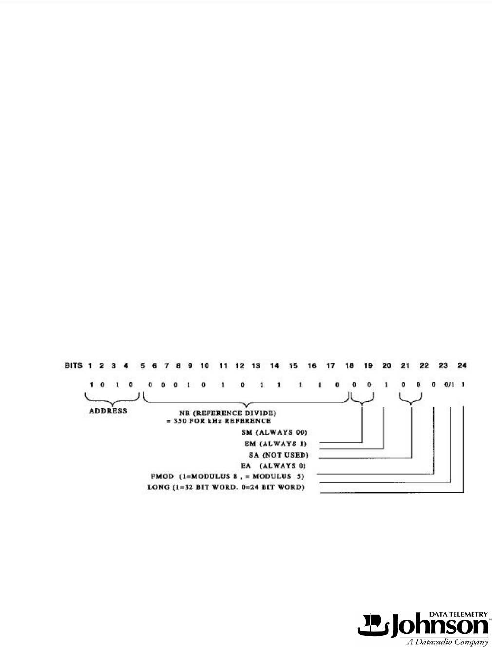
3.2 DM3474 SYNTHESIZER DATA PROTOCOL
Programming of the dividers and the charge pumps are performed on a 3-line bus; SYNTH ENABLE,
SYNTH DATA, AND SYNTH CLK. On initial power up three 34-bit words are required to load the 3474 Data
Transceiver. After the initial load, one 32-bit word can be used to change channels.
The SA7025 Synthesizer IC uses four address words; D, C, B and A (see Figure 3-4). The C word is not used
in the 3474. The 24- and 32-bit words contain one or four address bits, depending on the address bits, the data is
latched into registers. When the A-word is loaded, the data of these temporary registers is loaded together with the
A-word into the work
registers.
3.2.1 D-WORD
Refer to Figure 3-1.
TCXO Reference Frequency is 17.5 MHz.
Loop Reference Frequency is 50 kHz.
Reference Divide (NR) = 17.5 MHz ÷ 50 kHz =350 Decimal or 000101011110 Binary.
The 3474 has frequency resolution of 6.25 kHz and 10 kHz. When programming 6.25 kHz frequency
resolution use FMOD=8. When programming 10 kHz frequency resolution use FMOD=5.
Example:
(FCM) ÷ FMOD = 50 kHz ÷ 8 = 6.25 kHz
(FCM) ÷ FMOD = 50 kHz ÷ 5 = 10 kHz
Where:
FCM = Loop Reference Frequency
FMOD = Fractional N Modulus
Since FMC is the same for both 6.25 kHz and 10 kHz the loop dynamics are very similar and the same loop
filter values can be used.

PROGRAMMING
3-2
Part No. 001-3474-002
3.2.2 B-WORD
The B-Word is 24-bits long (see Figure 3-2). It contains the Address, Charge Pump setting factor (CN),
Binary Acceleration factors (CK, CL), and Prescaler Type (PR).
The Charge Pump Current setting (CN) could be changed on a channel-by-channel basis for ultimate rejection
of the Fraction N spurious responses close into the carrier frequency. The 3474 synthesizer has an adjust (R855)
for the fractional compensation current. The factory preset value will allow CN to be set to the following ranges:
Frequency in a Band CN
Lowest TX 86
Highest TX 90
Lowest RX 96
Highest RX 100
The value of CN should be interpolated for frequencies between the band edges. With these recommended
values of CN, the transceiver should have the fractional spurs minimized far below the levels needed to make ETSI
70 dB adjacent channel RX or TX
specifications.
Example:
Model 3474-530 is a 450-466 MHz transceiver.
458 MHz TX CN = 88 01011000 Binary
458 MHz RX CN = 98 01100010 Binary
3.2.3 A-WORD
The A-Word must be sent last (see Figure 3-3). The A-Word contains new data for the loop dividers and is
programmed for every channel. The A-Word can be a 24-bit or 32-bit word depending on the state of the flag
LONG in the D-Word. The 24-bit word (A0) is sent if LONG=0 and the 32-bit word (A1) is sent if LONG=1. The
extra 8-bits in A1 are the CN charge pump settings. Upon power up the D-, B- and A-Words must be sent, but after
that only the A1 word needs to be sent.
The Fractional-N increment (NF) is a 3-bit word that is channel dependent. NF is used to program the sub-
channels below the 50 kHz Loop Reference frequency. FCM = 50 kHz and if FMOD = 8, then the Fractional-N
increment is: 50 kHz ÷ 8 = 6.25 kHz
To program an 18.75 kHz channel:
NF = 18.75 kHz ÷ 6.25 kHz
NF = 3
PROGRAMMING
3-3
Part No. 001-3474-002
NM1 and NM2 are calculated as follows:
N = (NM1 + 2) x 64 + NM2 x 65 Where: N = total division ratio
NM1 = Number of main divider cycles when prescaler modulus equals 64
NM2 = Number of main divider cycles when prescaler modulus equals 65
Example:
Calculate NM1 and NM2 to Receive 454.500 MHz.
LO = 454.5 + 52.95 = 507.45 MHz
(52.95 MHz IF with High Side Injection)
N = RX LO ÷ FCM = 507.45 ÷ 0.05 = 10149
(FMC = Loop Reference Frequency)
NM2 = 64 x FRAC [N ÷ 64]
= 64 x FRAC [10149 ÷ 64]
= 64 x 0.57813
= 37
NM1 = INTEGER [N ÷ 64] - 2 - NM2
= 158 - 2 - 37
= 119
Figure 3-1 D-WORD

PROGRAMMING
3-4
Part No. 001-3474-002
Figure 3-2 B-WORD
Figure 3-3 A-WORD

PROGRAMMING
3-5
Part No. 001-3474-002
Figure 3-4 SERIAL INPUT WORD FORMAT
PROGRAMMING
3-6
Part No. 001-3474-002
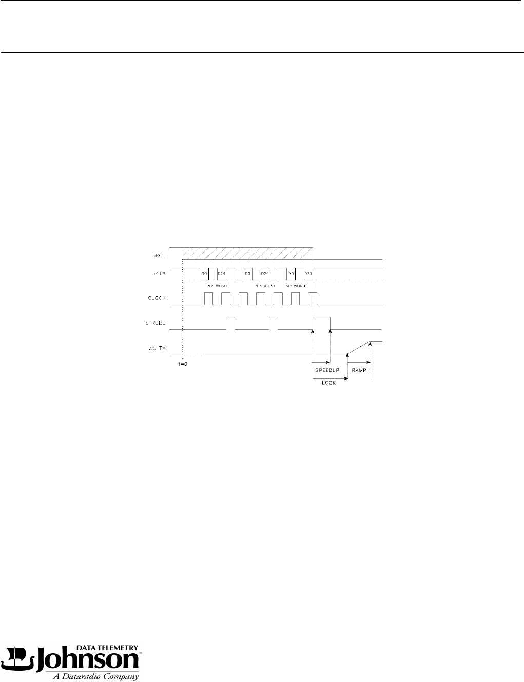
3.3 RECEIVE TO TRANSMIT SEQUENCE
Refer to Figure 3-5.
1. Synthesizer is loaded (B and A 24-Bit words or one long 32-bit A-Word).
2. The state of the 5RCL line does not have to be changed until the last bit is sent. However, RX will cease as soon
as it is changed.
3. The SYNTH ENABLE line should be held HIGH for 2 to 3 milliseconds after the last word is sent. This puts the
frequency synthesizer in a SPEEDUP MODE and slightly improves lock times.
4. After the last word is strobed in, 7 milliseconds (worst case) should elapse before 7.5 TX is turned ON. This
allows the synthesizer to come within 1 kHz of the desired frequency.
Figure 3-5 RX TO TX TIMING DIAGRAM
Dekey is a length of time to allow the TX to power down while the synthesizer is still in lock. This is needed
to meet ETSI (European Telecommunications Standards Institute) adjacent power specifications. Dekey is
approximately 3 ms in length. The 7.5 TX should be ramped or optimally filtered in such a way as to reduce the
Sinx/x power spreading. Speedup will slightly improve lock times and is 1 to 2 ms.
PROGRAMMING
3-7
Part No. 001-3474-002
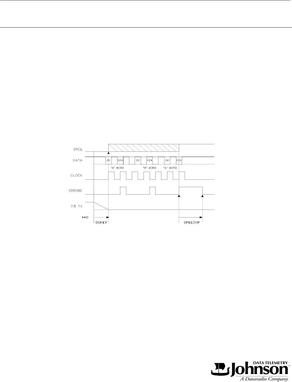
3.4 TRANSMIT TO RECEIVE SEQUENCE
Refer to Figure 3-6.
1. 7.5 TX is turned OFF. For best TX adjacent channel power performance this could be shaped.
2. The synthesizer load process could begin slightly before, but when the last bit is strobed in the synthesizer it will
become unlocked. For ETSI specs, the TX should be turned OFF “on-frequency”.
3. The 5RCL line should switch from low to high AFTER the 7.5 TX is switched. The 5RCL not only turns the RX
circuits on but also Pin Shifts the VCO.
4. For quickest lock times the SYNTH ENABLE line on the last load word should be held high for 2 to 3 millisec-
onds. It MUST NOT be left high as the synthesizer in the SPEEDUP mode has poor noise performance and
would degrade the RX performance.
Figure 3-6 TX TO RX TIMING DIAGRAM
Speedup is 2 to 3 ms
Lock is approximately 7 ms
Ramp is approximately 3 ms
IMPORTANT
If the receiver is to be operated at 510-512 MHz (-810), a spurious condition may occur to degrade the
receiver sensitivity 2 to 3 dB. If this degradation is unacceptable, the synthesizer can be reprogrammed to a
comparison frequency (FCM) of 31.25 kHz (so that a multiple of this would not be 52.95 MHz) and a modulus
(FMOD) of 5 with a reference divide (NR) of 560. These parameters place the spurious at harmonics of 31.25 kHz
(instead of 50 kHz) outside the passband of the IF filters where the sensitivity is not degraded.

PROGRAMMING
3-8
Part No. 001-3474-002
This page intentionally left blank.

SECTION 4
4-1
Part No. 001-3474-002
CIRCUIT DESCRIPTION
4.1 GENERAL
4.1.1 INTRODUCTION
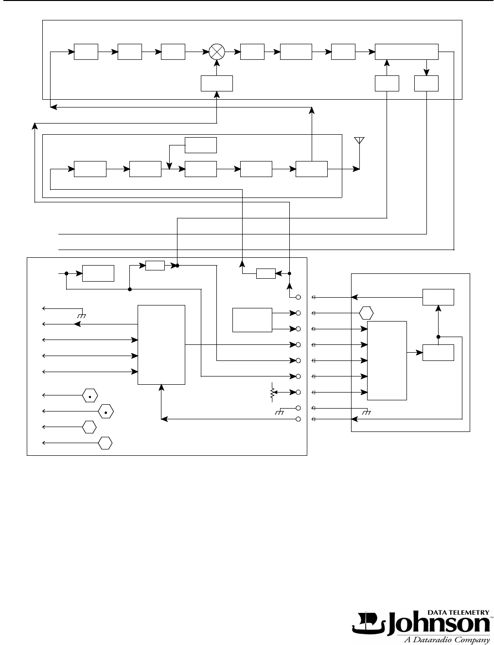
The main subassemblies of this transceiver are the RF board, VCO board, and TCXO. A block diagram of the
transceiver is located in Figure 4-1.
The VCO board is enclosed by a metal shield and soldered directly to the RF board. The VCO is not
serviceable.
The 3474 is available with a reference oscillator stability of ±1.5 PPM. The TCXO (Temperature
Compensated Crystal Oscillator) is soldered directly to the RF board.
4.1.2 SYNTHESIZER
The VCO (voltage-controlled oscillator) output signal is the receiver first injection frequency in the Receive
mode and the transmit frequency in the Transmit mode. The first injection frequency is 52.95 MHz above the
receive frequency. The frequency of this oscillator is controlled by a DC voltage produced by the phase detector in
synthesizer chip U801.
Channels are selected by programming counters in U801 to divide by a certain number. This programming is
performed over a serial bus formed by the Synth Clock, Synth Enable, and Synth Data pins of J201. This
programming is performed by user supplied hardware and software (see Section ).
The frequency stability of the synthesizer in both the receive and transmit modes is established by the
stability of the reference oscillator described in the preceding section. These oscillators are stable over a
temperature range of -30° to +60° C (-22° to +140° F).
4.1.3 RECEIVER
The receiver is a double-conversion type with intermediate frequencies of 52.95 MHz / 450 kHz. Two helical
bandpass filters reject the image, half IF, injection, and other unwanted frequencies. A four-pole crystal filter
enhances receiver selectivity

CIRCUIT DESCRIPTION
4-2
Part No. 001-3474-002
4.1.4 TRANSMITTER
The transmitter produces a nominal RF power output of 2W adjustable to 500 mW (-XX0). Frequency
modulation of the transmit signal occurs in the synthesizer. Transmit audio processing circuitry is contained in the
customer-supplied equipment.
4.2 SYNTHESIZER
4.2.1 INTRODUCTION
A block diagram of the synthesizer is shown in Figure 4-1 and a block diagram of Synthesizer IC U801 is
shown in Figure 4-2. As stated previously, the synthesizer output signal is produced by a VCO (voltage controlled
oscillator). The VCO frequency is controlled by a DC voltage produced by the phase detector in U801. The phase
detector senses the phase and frequency of the two input signals and causes the VCO control voltage to increase or
decrease if they are not the same. The VCO is then “locked” on frequency.
Programming of the synthesizer provides the data necessary for the internal prescaler and counters. One input
signal is the reference frequency. This frequency is produced by the 17.5 MHz reference oscillator (TCXO). The
other input signal is the VCO frequency.
CIRCUIT DESCRIPTION
4-3
Part No. 001-3474-002
Figure 4-1 DATA TRANSCEIVER BLOCK DIAGRAM
Z201
RF AMP
Q201 Z202
MIXER
CRYSTAL FILTER
PREDRIVER
Q501
DRIVER FINAL ANTENNA
SWITCH
RX AUDIO
VCO
+5V
+5V
+7.5V
+7.5V
RECEIVE
TRANSMIT
LOCK
ENABLE
DATA
CLOCK
AMPLIFIER
+5V
T/R PS
NEG SUP
RECEIVER
TRANSMITTER
SYNTHESIZER
VCO BUFFER/
RSSI
ANTENNA
LOW-PASS
FILTER
RF OUT
RF BPF RF BPF U221
Z221/Z222
52.95 MHz
Q222
IF / 450 kHz FILTER
Q521 Q541 CR561/562,
U542
Q401
2nd LO AMP
1st LO AMP
Q851
CLV
Q853
Q851/Q852
AMPLIFIER
RSSI
RX OUT
TX IN Y801
TCXO
MOD INPUT
MOD ADJUST
SYNTH OUT
RF IN
U801
Q833
Q101, Q102
Q831, Q832
Q834
BUFFER
U241
U251Q301
IF AMP
Q221
Q850

CIRCUIT DESCRIPTION
4-4
Part No. 001-3474-002
Figure 4-2 U801 SYNTHESIZER BLOCK DIAGRAM
CLOCK
DATA
STROBE
Vss
RF
IN
RF
IN
64/65/72
PRESCALER MAIN DIVIDERS
EM FB 2 2 12 8
PR NM1 NM3
NM2
FRACTIONAL
ACCUMULATOR
PRESCALER
MODULUS
CONTROL
3FMOD NF
FB
SERIAL INPUT + PROGRAM LATCHES VDD
TEST
IN
REF
EM+EA
REFERENCE DIVIDER +2 +2 +2
MAIN
MAIN
PHASE
DETECTOR
REFERENCE
SELECT
2
SM
EM
REFERENCE
SELECT
2
SA
SECONDARY
PHASE
DETECTOR
EA
AUXILIARY
IN
EA
AUX
12
NR
12
NAPA
AUXILIARY DIVIDER
PRESCALER
1/4
NORMAL
OUTPUT
CHARGE
PUMP
OUTPUT
CHARGE
PUMP
SPEED-UP
OUTPUT
CHARGE
PUMP
INTEGRAL
OUTPUT
CHARGE
PUMP
AUXILIARY
CN
8
CL
2
CK
4
2
VSSA
V
DDA
LOCK
PHA
RA
PHI
PHP
RN
RF

CIRCUIT DESCRIPTION
4-5
Part No. 001-3474-002
4.2.2 VOLTAGE-CONTROLLED OSCILLATOR
Oscillator (Q850)
The VCO is formed by Q850, several capacitors and varactor diodes, and a ceramic resonator. It oscillates at
the transmit frequency in transmit mode and first injection frequency in the receive mode (approximately 450
MHz in transmit and 500 MHz in receive).
Biasing of Q850 is provided by R862, R867 and R868. An AC voltage divider formed by C859, C861 and
C862 initiates and maintains oscillation and also matches Q850 to the tank circuit. The ceramic resonator is
grounded at one end to provide shunt inductance to the tank circuit.
Frequency Control and Modulation
The VCO frequency is controlled in part by DC voltage across varactor diodes CR854, CR855, CR856 and
CR851. As voltage across a reverse-biased varactor diode increases, its capacitance decreases. Therefore, VCO
frequency increases as the control voltage increases. CR854/CR855 and CR856/CR851 are paralleled varactor to
divide the capacitance and improve linearity. The varactors are biased at -2V to adjust to the voltage output of
U801. The control line is isolated from tank circuit RF by choke L851 and L854 and decoupling capacitor C854.
The amount of frequency change produced by CR854/CR855/CR856/CR851 is controlled by series capacitor
C853.
The -2V applied to the VCO is derived from the TCXO frequency that is amplified by Q833, rectified by
CR831 and filtered by C844, C845, C846 and C847 on the RF board.
The VCO frequency is modulated using a similar method. The transmit audio/data signal is applied across
varactor diode CR852 which varies the VCO frequency at an audio rate. Series capacitors C856/C870 set the
amount of deviation produced along with CR853 and C858. R854 provides a DC ground on the anodes of CR852/
CR853, and isolation is provided by R852 and C855.
The DC voltage across CR853 provides compensation to keep modulation relatively flat over the entire
bandwidth of the VCO. This compensation is required because modulation tends to increase as the VCO frequency
gets higher (capacitance of CR854/CR855/CR856/CR851 gets lower). CR853 also balances the modulation
signals applied to the VCO and TCXO. An external voltage from J201, pin 14 can also adjust the modulation.
The DC voltage applied across CR853 comes from the modulation adjust control R810. R811 applies a DC
biasing voltage to CR852; C814 provides DC blocking; and C818 attenuates AC signals applied through R811. RF
isolation is provided by C858, R853, C817 and R812.

CIRCUIT DESCRIPTION
4-6
Part No. 001-3474-002
4.2.3 VCO AND REFERENCE OSCILLATOR MODULATION
Both the VCO and reference oscillator (TCXO) are modulated in order to achieve the required frequency
response. If only the VCO was modulated, the phase detector in U801 would sense the frequency change and
increase or decrease the VCO control voltage to counteract the change (especially at the lower audio frequencies).
If only the reference oscillator frequency is modulated, the VCO frequency would not change fast enough
(especially at the higher audio frequencies). Modulating both VCO and reference oscillators produces a flat audio
response. Potentiometer R810 sets the VCO modulation sensitivity so that it is equal to the reference oscillator
modulation
sensitivity.
4.2.4 CASCODE AMPLIFIERS (Q851/Q852)
The output signal on the collector of Q850 is coupled by L861/C864 to buffer amplifier Q851/Q852. This is a
shared-bias amplifier which provides amplification and also isolation between the VCO and the stages which
follow. The signal is direct coupled from the collector of Q852 to the emitter of Q851. The resistors in this circuit
provide biasing and stabilization, and C865 and C866 are bypass capacitors.
4.2.5 AMPLIFIER (Q853)
Amplifier Q853 provides amplification and isolation between the VCO and receiver and transmitter. C868
provides matching between the amplifiers. Bias for Q853 is provided by R871, R872 and R874. Inductor L856 and
capacitor C873 provide impedance matching on the output.
4.2.6 VOLTAGE FILTER (Q832)
Q832 is a capacitance multiplier to provide filtering of the 4.6V supply to the VCO. R836 provides transistor
bias and C834 provides the capacitance that is multiplied. If a noise pulse or other voltage change appears on the
collector, the base voltage does not change significantly because of C834. Therefore, base current does not change
and transistor current remains constant. CR832 decreases the charge time of C834 when power is turned on. This
shortens the start-up time of the VCO. C841, C840 and C855 are RF decoupling capacitors.
4.2.7 VCO FREQUENCY SHIFT (Q831)
The VCO must be capable of producing frequencies from approximately 403-564.95 MHz to produce the
required receive injection and transmit frequencies. If this large of a shift was achieved by varying the VCO
control voltage, the VCO gain would be undesirably high. Therefore, capacitance is switched in and out of the tank
circuit to provide a coarse shift in frequency.
This switching is controlled by the T/R pin shift on J201, pin 4, Q831/Q834 and pin diode CR850. When a pin
diode is forward biased, it presents a vary low impedance to RF; and when it is reverse biased, it presents a very
high impedance. The capacitive leg is switched in when in transmit and out when in receive.

CIRCUIT DESCRIPTION
4-7
Part No. 001-3474-002
When J201, pin 4 is high in receive, Q834 is turned off, Q101 is turned on and the collector voltage goes low.
A low on the base of Q102 turns the transistor on and the regulated +5.5V on the emitter is on the collector for the
receive circuitry. With a low on the base of Q831 the transistor is off and the collector is high. With a high on the
collector of Q831 and a low on the emitter of Q834, this reverse biases CR850 for a high impedance.
The capacitive leg is formed by C851, CR850, C852 and C876. When J201, pin 4 is low in transmit, Q834 is
turned on and a high is on the emitter, Q101 is turned off and the collector voltage goes high. A high on the base of
Q102 turns the transistor off and the regulated +5.5V is removed from the receive circuitry. With a high on the
base of Q831 the transistor is on and the collector is low. With a low on the collector of Q831 and a high on the
emitter of Q834, this forward biases CR850 and provides an RF ground through C851 and C852/C876 are
effectively connected to the tank circuit. This decreases the resonant frequency of the tank circuit.
4.2.8 SYNTHESIZER INTEGRATED CIRCUIT (U801)
Introduction
Synthesizer chip U801 is shown in Figure 4-2. This device contains the following circuits: R (reference),
Fractional-N, NM1 and NM2; phase and lock detectors, prescaler and counter programming circuitry. The basic
operation was described in Section 4.2.1.
Channel Programming
Frequencies are selected by programming the R, Fractional-N, NM1 and NM2 in U801 to divide by a certain
number. These counters are programmed by a user supplied programming circuit. More information on
programming is located in Section .
As previously stated, the counter divide numbers are chosen so that when the VCO is oscillating on the
correct frequency, the VCO-derived input to the phase detector is the same frequency as the reference oscillator-
derived frequency.
The VCO frequency is divided by the internal prescaler and the main divider to produce the input to the phase
detector.
4.2.9 LOCK DETECT
When the synthesizer is locked on frequency, the SYNTH LOCK output of U801, pin 18 (J201, pin 7) is a
high voltage. Then when the synthesizer is unlocked, the output is a low voltage. Lock is defined as a phase
difference of less than 1 cycle of the TCXO.

CIRCUIT DESCRIPTION
4-8
Part No. 001-3474-002
4.3 RECEIVER CIRCUIT DESCRIPTION
4.3.1 HELICAL FILTER (Z201), RF AMPLIFIER (Q201)
Capacitor C201 couples the receive signal from the antenna switch to helical filter Z201. (The antenna switch
is described in Section 4.4.5.) Z201 is a bandpass filter tuned to pass only a narrow band of frequencies to the
receiver. This attenuates the image and other unwanted frequencies. The helicals are factory set and should not be
tuned.
Impedance matching between the helical filter and RF amplifier Q201 is provided by C203, C204 and L201.
Q201 amplifies the receive signal to recover filter losses and also to increase receiver sensitivity. Biasing for Q201
is provided by R201, R202 and R203; and C208/C209 provide RF bypass. CR201 protects the base-emitter
junction of Q201 from excessive negative voltages that may occur during high signal conditions. Additional
filtering of the receive signal is provided by Z202. L202, and C205 provide impedance matching between Q201
and Z202. Resistor R204 is used to lower the Q of L202 to make it less frequency selective.
4.3.2 MIXER (U221), FIRST LO AMPLIFIER (Q301)
First mixer U221 mixes the receive frequency with the first injection frequency to produce the 52.95 MHz
first IF. Since high-side injection is used, the injection frequency is 52.95 MHz above the receive frequency. The
RF signal is coupled to the mixer through C206.
The first injection frequency from the VCO is coupled to the first local oscillator amplifier Q301 through
C301. L301 and C302 match Q301 to the VCO. Bias for Q301 is provided by R301, R302 and R303, and C303
decouples RF signals. Impedance matching to the mixer is provided by L302, R304 and C304.
4.3.3 AMPLIFIER (Q222), CRYSTAL FILTER (Z221/Z222), IF AMP (Q221)
The output of U221 is coupled to buffer Q222. C222, R229 and Q222 match the 50 ohm output of U221. Bias
for Q222 is provided by R228 and R229. The output of Q222 is matched to crystal filter Z221 via L222, C223 and
R230. This filter presents a low impedance to 52.95 MHz and attenuates the receive, injection, and other
frequencies outside the 52.95 MHz passband.
Z221 and Z222 form a 2-section, 4-pole crystal filter with a center frequency of 52.95 MHz and a -3 dB
passband of 8 kHz (12.5 kHz BW) or 15 kHz (20/25 kHz BW). This filter establishes the receiver selectivity by
attenuating the adjacent channel and other signals close to the receive frequency. C232, C224, and L223 adjust the
coupling of the filter. L224, C225 and C227 provide impedance matching between the filter and Q221.
IF amplifier Q221 amplifies the 52.95 MHz IF signal to recover filter losses and improves receiver sensitivity.
Biasing for Q221 is provided by R222, R223, R225 and R226 and C228, C229 decouple RF signals. The output of
Q221 is coupled to the detector by C230.

CIRCUIT DESCRIPTION
4-9
Part No. 001-3474-002
4.3.4 SECOND LO AMP/TRIPLER (Q401), SECOND IF FILTER (Q901)
The input frequency to Q401 is 17.5 MHz from TCXO Y801 coupled through C402. Bias for Q401 is
provided by R401, R402, R403 and R404. C403, C404 decouple RF from the amplifier. L401, L402, C405, C406
and C407 pass the third harmonic of the input (52.5 MHz) to U241, pin 1. The output of the amplifier is coupled to
U241, pin 1 by C241, and C410 and L404 provided low frequency decoupling.
4.3.5 SECOND MIXER/DETECTOR (U241)
Oscillator and Mixer
As shown in Figure 4-3, U241 contains the second oscillator, second mixer, limiter, detector, and squelch
circuitry. The 52.95 MHz IF signal is mixed with a 52.5 MHz signal produced by second LO amplifier Q401 from
TCXO Y801.
Figure 4-3 U241 BLOCK DIAGRAM
1
2
3
4
DEMODULATOR
MIXEROSCILLATOR
5
6
7
8
LIMITER
AMP
AMP
16
15
14
13
10
12
11
9
AUDIO OUT
NC
NC
MIXER IN
L242
C243
C242
Z241
Z242
52.5 MHz C410
L404
C241
AF
RSSI
5.5V CONT

CIRCUIT DESCRIPTION
4-10
Part No. 001-3474-002
Second IF Filter
The output of the internal double-balanced mixer is the difference between 52.95 MHz and 52.5 MHz which
is 450 kHz. This 450 kHz signal is fed out on pin 3 and applied to second IF filters Z241 and Z242. These filters
have passbands of 9 kHz (12.5 kHz BW), 15 kHz (20 kHz BW) or 20 kHz (25 kHz BW) at the
-6 dB points and are used to attenuate wideband noise.
Limiter-Amplifier
The output of Z241/Z242 is applied to a limiter-amplifier circuit in U241. This circuit amplifies the 450 kHz
signal and any noise present; then limits this signal to a specific value. When the 450 kHz signal level is high,
noise pulses tend to get clipped off by the limiter; however, when the 450 kHz signal level is low, the noise passes
through. C242, C243 decouple the 450 kHz signal.
Quadrature Detector
From the limiter stage the signal is fed to the quadrature detector. An external phase-shift network connected
to pin 8 shifts the phase of one of the detector inputs 90° at 450 kHz (all other inputs are unshifted in phase). When
modulation occurs, the frequency of the IF signal changes at an audio rate as does the phase of the shifted input.
The detector, which has no output with a 90° phase shift, converts this phase shift into an audio signal. L242 is
tuned to provide maximum undistorted output from the detector. R242 is used to lower the Q of L242. From the
detector the audio and data signal is fed out on pin 9.
Audio/Data Amplifier
The audio/data output of U241 on pin 9 is fed to the audio amplifier U261. U261 amplifies the detected
audio/data signal and shifts the DC bias level to 2.5V. The gain is set at approximately 1.5 by R261/R262. R263
and R264 provide a 1.9V DC reference bias voltage. The audio output of U261 is applied to J201, pin 13.
Receive Signal Strength Indicator (RSSI)
U241, pin 13 is an output for the RSSI circuit which provides a current proportional to the strength of the 450
kHz IF signal. The voltage developed across R241 is applied to J201, pin 12.
4.4 TRANSMITTER CIRCUIT DESCRIPTION
4.4.1 BUFFER (Q851)
The output signal is applied to a 50-ohm pad formed by R851, R852, and R853. This pad provides attenuation
and isolation. Q851 provides amplification and also additional isolation between the VCO and transmitter. Biasing
for this stage is provided by R854, and decoupling of RF signals is provided by C852. Impedance matching with
the transmitter is provided by L501 and C502.

CIRCUIT DESCRIPTION
4-11
Part No. 001-3474-002
4.4.2 PRE-DRIVER (Q501), DRIVER (Q521)
Pre-driver Q501 is biased class A by R501 and R502 and R506. L501 and C502 match Q501 to Q851. C520
and C508 bypass RF from the DC line, and R503 provides supply voltage isolation. R507 ties the +7.5V supply to
the circuit for high power applications and R508 ties the circuit to +5V for low power applications. Impedance
matching between Q501 and Q521 is provided by L502, L503 and C511. R504 and C504 provide negative
feedback to prevent
oscillation.
Driver Q521 is biased nearly Class C by R521 and R522. Impedance matching with Q541 is provided by
L521, C525, C527, L522 and C526.
4.4.3 -5V POWER CONTROL SUPPLY
The 17.5 MHz from the TCXO is coupled through C902 to Q901. Bias for Q901 is provided by R903, R904,
R901, R902 and R905. C901 and C903 provide RF decoupling. The amplified signal rectified by CR901/CR902 to
produce a -5V DC source. C909 stabilizes the voltage level and C910 and C911 provide RF decoupling. This -5V
source is used in the transmit power control circuit U542.
4.4.4 FINAL (Q541), POWER CONTROL (U542)
Q541 is biased for Class C operation. The output is matched to the low-pass filter by L541, C552, and several
capacitors. The supply voltage is isolated from RF by ferrite bead EP541.
Power control is provided by U542. The 5.5V transmit supply is passed by U542 to power adjust R542. The
other end of R542 is the rectified -5V from Q901. This negative voltage is required when low power is used to
pinch off Q541 to the required output.
The low-pass filter consists of L561, C561, L562, C562, L563, C563 and L564. The filter attenuates spurious
frequencies occurring above the transmit frequency band. The transmit signal is then fed through the antenna
switch to antenna jack J501.
4.4.5 ANTENNA SWITCH (CR561, CR562)
The antenna switching circuit switches the antenna to the receiver in the receive mode and the transmitter in
the transmit mode. In the transmit mode, +7.5V is applied to L565 and current flows through diode CR561, L566,
diode CR562, and R562/R563. When a diode is forward biased, it presents a low impedance to the RF signal;
conversely, when it is reverse biased (or not conducting), it presents a high impedance (small capacitance).
Therefore, when CR561 is forward biased, the transmit signal has a low-impedance path to the antenna through
coupling capacitor C568.

CIRCUIT DESCRIPTION
4-12
Part No. 001-3474-002
C567, L566, and C570 form a discrete quarter- wave line. When CR561 is forward biased, this quarter-wave
line is effectively AC grounded on one end by C570. When a quarter-wave line is grounded on one end, the other
end presents a high impedance to the quarter-wave frequency. This blocks the transmit signal from the receiver.
C569 matches the antenna to 50 ohms in transmit and receive.
In the receive mode, no power is applied to L565, so all the diodes are “off”. The receive signal then has a
high-impedance path into the transmitter and a low-impedance path into the receiver because the quarter-wave line
is not grounded.

5-1
Part No. 001-3474-002
SECTION 5
SERVICING
5.1 GENERAL
5.1.1 PERIODIC CHECKS
This transceiver should be put on a regular maintenance schedule and an accurate performance record
maintained. Important checks are receiver sensitivity and transmitter frequency, modulation, and power output. A
procedure for these and other tests is located in Section 6. It is recommended that transceiver performance be
checked annually even though periodic checks are not required by the FCC. During the first year, make an
additional check or two to ensure no TCXO frequency drifting has occurred.
5.1.2 SURFACE-MOUNTED COMPONENTS
A large number of the components used on the transceiver board are the surface-mounted type. Since these
components are relatively small in size and are soldered directly to the PC board, care must be used when they are
replaced to prevent damage to the component or PC board. Surface-mounted components should not be reused
because they may be damaged by the unsoldering process.
5.1.3 SCHEMATIC DIAGRAMS AND COMPONENT LAYOUTS
Schematic diagrams and component layouts of the PC boards used in this transceiver are located in Section 8.
A component locator guide is also provided to aid in component location.
5.1.4 REPLACEMENT PARTS LIST
A replacement parts list with all the parts used in this transceiver is located in Section 7. Parts are listed alpha-
numerically according to designator. For information on ordering parts, refer to Section 1.8.
5.1.5 TCXO MODULE NOT SERVICEABLE
The ±1.5 PPM TCXO module is not field serviceable. Part changes require a factory recalibration to ensure
that the oscillator stays within its ±1.5 PPM tolerance.
5.2 SYNTHESIZER SERVICING
5.2.1 INTRODUCTION
When there is a synthesizer malfunction, the VCO is not locked on frequency. When an unlocked VCO is
detected by the lock detector circuit, U801, pin 18 goes low (0V).

SERVICING
5-2
Part No. 001-3474-002
NOTE: The user-supplied circuitry must disable the transmitter and receiver when an out-of-lock condition is
indicated.
When the VCO is unlocked, the fR and fV inputs to the phase detector are usually not in phase (see Section
4.1.2). The phase detector in U801 then causes the VCO control voltage to go to the high or low end of its
operating range. This in turn causes the VCO to oscillate at the high or low end of its frequency range.
As shown in Figure 4-1, a loop is formed by VCO Q850, amplifier Q851/Q852, and the RF IN of U801.
Therefore, if any of these components begin to malfunction, improper signals appear throughout the loop.
However, correct operation of the counters can still be verified by measuring the input and output frequencies to
check the divide number.
Proceed as follows to check the synthesizer I/O signals to determine if it is operating properly.
5.2.2 REFERENCE OSCILLATOR
Check the signal at U801, pin 8. It should be 17.5 MHz at a level of approximately 1.5V P-P. If the TCXO
module is defective, it is not serviceable and must be replaced with a new module as described in Section 5.1.5.
5.2.3 VCO
Output Level
The output level of Q853 can be measured with an RF voltmeter or some other type of high impedance meter.
The minimum level after a power splitter at R851 should be -10 dBm.
Control Voltage
Check the DC voltage at C815 with a channel near the center of the band. If the VCO is locked on frequency,
this should be a steady DC voltage near 3V. If it is not locked on frequency, it should be near the lower or upper
end of its range (0V or 5.5V).
Output Frequency
Check the VCO frequency at R851. If the VCO is locked on frequency, it should be stable on the transmit
channel frequency. If the VCO is not locked on frequency, the VCO control voltage is probably near 0V or 5.5V.
5.2.4 SYNTHESIZER (U801)
Lock Detector
When the VCO is locked on frequency, the lock detect output on J201, pin 7 should be high.

SERVICING
5-3
Part No. 001-3474-002
5.3 RECEIVER SERVICING
To isolate a receiver problem to a specific section, refer to the troubleshooting flowchart in Figure 5-1. Tests
referenced in the flowchart are described in the following information.
NOTE: Supply voltages are provided by the user.
5.3.1 SUPPLY VOLTAGES AND CURRENT
Measure the supply voltages on the following pins at interface connector J201:
Pin 4 - 5.0V DC Receive
Pin 5 - 5.0V DC
Place a DC ammeter in the supply line to the transceiver and the following maximum currents should be
measured:
Pin 4 - 10 mA
Pin 5 - 50 mA
5.3.2 MIXER/DETECTOR (U201)
Data Output
Using a .01 µF coupling capacitor, inject at U241, pin 16, a 52.95 MHz, 1 mV signal, modulated with 1 kHz
at ± 3 kHz deviation. The audio output level at U241, pin 9 should be approximately 400 mV RMS.
The data output on J201, pin 13 should be 600 mV to 1.2V P-P or 212 mV to 424 mV RMS with the
preceding injection signal.
RSSI Output
The RSSI output on J201, pin 12 should be greater than 100 mV at 12 dB SINAD and less than 2.5V with 1
mV input. If either of the preceding measurements is not correct, there may be a problem with U241.

SERVICING
5-4
Part No. 001-3474-002
Figure 5-1 RECEIVER SERVICING FLOWCHART
5.3.3 RF AMPLIFIER (Q201) AND FIRST MIXER (Q221)
Refer to the schematic diagram for signal levels and test points for measuring levels.
5.3.4 RF AND IF AMPLIFIERS, FIRST MIXER
Check the DC voltages shown on the schematic diagram. If they are normal, inject a signal at the input and
output of each stage using a .01 µF coupling capacitor. If the stage is producing gain, the injection level on the
input of a stage should be less than that required on the output to produce the same SINAD at the receive output.
5.4 TRANSMITTER SERVICING
5.4.1 SUPPLY VOLTAGES AND CURRENT
Measure the supply voltages on the following pins of interface connector J201:

SERVICING
5-5
Part No. 001-3474-002
Pin 2 - 7.5V DC
Pin 3 - 7.5V DC
Pin 4 - 0.0V DC (while transmitting)
Pin 5 - 5.0V DC
Pin 6 - 2.5V DC Transmit In/1.5V P-P max
Place a DC ammeter in the supply line to the transceiver and the following maximum currents should be
measured:
Pin 2 - 650 mA
Pin 3 - 250 mA
Pin 5 - 12 mA
Figure 5-2 TRANSMITTER SERVICING FLOWCHART

SERVICING
5-6
Part No. 001-3474-002
This page intentionally left blank.

SECTION 6
6-1
Part No. 001-3474-002
ALIGNMENT PROCEDURE AND PERFORMANCE TESTS
6.1 GENERAL
Receiver or transmitter alignment may be necessary if repairs are made that could affect tuning. Alignment
points diagrams are located in Figure 6-3 or component layouts are located in Section 8.
Fabricate test cables by referring to Section 2.2, Interfacing with Data Equipment. This cable should include
power and ground, a transmit keying switch that shorts the keying line to ground, data input and data output. The
test setup must apply the various supply voltages and load the synthesizer with channel information.
6.2 DL3474 TRANSCEIVER ONLY
6.2.1 FREQUENCY AND CONTROL LINE VOLTAGE CHECK
1. Connect the test setup shown in Figure 6-1. Set the power supply for +7.5V DC.
2. Load the synthesizer with the channel frequency (see Section 3.2).
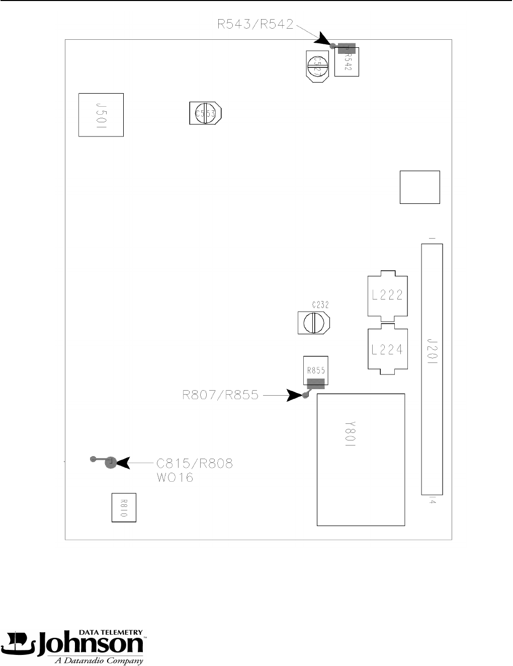
3. Connect a DC voltmeter at the junction of R808/C815 to measure the VCO control line voltage for a meter
reading of ≥0.50 - ≤4.90V DC (see Figure 6-3).
4. Key the transmitter.
5. Measure the VCO control line voltage for a meter reading of ≥0.75 - ≤5.00V DC
6. Unkey the transmitter.
6.2.2 2W TRANSMITTER POWER ALIGNMENT
1. Connect the test setup shown in Figure 6-1. A DC ammeter capable of measuring up to 1.5A should be installed
in the supply line.
2. Load the synthesizer with the center channel frequency.
3. Key the transmitter and make sure that the supply voltage at the RF board is 7.5V.
(Do not transmit for extended periods.)
4. Adjust C553 counterclockwise for minimum current.
5. Connect a voltmeter to the junction of R542/R543.

ALIGNMENT PROCEDURE AND PERFORMANCE TESTS
6-2
Part No. 001-3474-002
6. Adjust R542 clockwise for 2.30V DC (+0/-0.1V DC).
7. Readjust C553 counterclockwise for minimum current.
8. Tune C527 clockwise for maximum power.
9. Tune C553 clockwise for 2.0W (±0.1W). Current should be less than 900 mA. (Power output should be 1.6-2.4W
and current less than 900 mA from 403-512 MHz.)
10. Monitor the frequency with a frequency counter and adjust TCXO (Y801) for the channel frequency ±100 Hz.
Figure 6-1 TRANSMITTER TEST SETUP
6.2.3 LOW POWER ALIGNMENT
1. Connect the test setup shown in Figure 6-1.
2. Load the synthesizer with the center channel frequency.
3. Connect a voltmeter to the junction of R542/R543.
4. Adjust R542 clockwise for -1.5V DC (±0.1V DC).
5. Tune C527 clockwise for maximum power.

ALIGNMENT PROCEDURE AND PERFORMANCE TESTS
6-3
Part No. 001-3474-002
6. Tune C553 clockwise for minimum power.
7. Adjust R542 for the required power level.
8. Tune C527 for power balance at frequencies which are as close as possible to ±5 MHz from the center of the
channel frequency.
9. Re-adjust R542 for the power level required if necessary.
10. Monitor the frequency with a frequency counter and adjust TCXO (Y801) for the channel frequency ±100 Hz.
6.2.4 MODULATION FLATNESS ALIGNMENT
1. Inject a 220 Hz square-wave tone at approximately 0.35V P-P, biased at 2.5V DC on J201, pin 6.
2. Transmit into the modulation analyzer and observe modulation output on the oscilloscope. Set the modulation
analyzer high pass filtering off and no less than a 15 kHz low pass filter.
3. Adjust R810 for a flat square-wave on the oscilloscope.
4. Inject a 1 kHz sine-wave on J201, pin 6, biased at 2.5V DC, at the level below according to the bandwidth:
0.200V RMS for 12.5 kHz BW (-X10 Radios)
0.330V RMS for 20.0 kHz BW (-X20 Radios)
0.400V RMS for 25.0 kHz BW (-X30 Radios)
5. Switch on TX Modulation. Set the modulation analyzer for 3 kHz low pass filtering.
6. The transmit deviation should measure between:
±1.2/±1.9 kHz for 12.5 kHz BW (-X10 Radios)
±1.9/±3.0 kHz for 20.0 kHz BW (-X20 Radios)
±2.4/±3.8 kHz for 25.0 kHz BW (-X30 Radios)
7. Set a 0 dB reference on the Audio Analyzer.
8. Input a 100 Hz sine-wave. The level should be within ±1.5 dB of the 1 kHz reference.
9. Remove transmit modulation and unkey the transmitter.
10.Connect a DC voltmeter at the junction of R807/R855.
11.Adjust R855 to 2.10V DC (±0.05V DC).

ALIGNMENT PROCEDURE AND PERFORMANCE TESTS
6-4
Part No. 001-3474-002
Figure 6-2 RECEIVER TEST SETUP
6.2.5 RECEIVER ALIGNMENT
C A U T I O N: Do not key the transmitter with the generator connected! Severe generator damage may result.
1. Connect the test setup shown in Figure 6-2. Adjust the power supply for +7.5V DC.
2. Measure the receive current drain. (Typically current should be <80 mA.)
3. Preset tuning slugs of L222/L224 to the full clockwise position (slug in all the way).
4. Preset C232 to center position (slot in-line with axis of part).
5. Readjust L224 counterclockwise 2 turns.
6.2.6 IF AND AUDIO ADJUSTMENTS
1. Load the synthesizer with the channel frequency.
2. Set the RF signal generator for this frequency with a 1 kHz tone (modulated output shown below) at a level of
-47 dBm (1000 µV) and inject into J501.
1.5 kHz deviation (-X10 12.5 kHz BW Radio)
2.4 kHz deviation (-X20 20.0 kHz BW Radio)
3.0 kHz deviation (-X30 25.0 kHz BW Radio)

ALIGNMENT PROCEDURE AND PERFORMANCE TESTS
6-5
Part No. 001-3474-002
NOTE: Maintain these deviation levels throughout the test when measuring AC levels, SINAD and
% distortion.
3. Adjust L242 for 2.5V DC (±0.05V DC) at the receive audio output.
4. Set the RF signal generator level to -105 dBm, “unmodulated”.
5. Set the generator frequency 3 kHz below channel center (-X10) or 5 kHz below channel center (-X20/-X30).
6. Adjust C232, then L222 for peak RSSI voltage.
NOTE: Use 2V scale on DVM.
7. Set the RF signal generator frequency back to channel center at -47 dBm with standard deviation level.
8. Adjust L224 for minimum distortion.
9. Set the RF signal generator to -105 dBm, “unmodulated”.
10.Adjust L222 for peak RSSI voltage.
NOTE: Use 2V scale on DVM.
11 Adjust deviation to the level in Step 2. Record the RMS voltage level _______RMS. (Typically 300 mV ±50
mV.)
12.Record the percent distortion _______%. (Typically <3%.)
13.Adjust the RF input level until 12 dB SINAD is measured. (Typically <0.45 µV).
14. Adjust the generator RF level to -120 dBm and measure DC (RSSI) voltage on J201, pin 12. (Typically ≤ 0.90V
DC.)
15.Adjust the generator RF level to -60 dBm and measure DC (RSSI) voltage on J201, pin 12. (Typically ≥ 2.40V
DC.)
ALIGNMENT PROCEDURE AND PERFORMANCE TESTS
6-6
Part No. 001-3474-002
Figure 6-3 ALIGNMENT POINTS DIAGRAM
R509

SECTION 7
7-1
Part No. 001-3474-002
PARTS LIST
. 023-3474-515
SYMBOL
NUMBER DESCRIPTION PART
NUMBER
A 801 FINISHED 450-466 VCO(M9 023-3474-540
C 101 68pF 5% NPO 0603 610-3674-680
C 102 68pF 5% NPO 0603 610-3674-680
C 103 68pF 5% NPO 0603 610-3674-680
C 104 68pF 5% NPO 0603 610-3674-680
C 105 68pF 5% NPO 0603 610-3674-680
C 106 68pF 5% NPO 0603 610-3674-680
C 107 68pF 5% NPO 0603 610-3674-680
C 108 68pF 5% NPO 0603 610-3674-680
C 109 68pF 5% NPO 0603 610-3674-680
C 110 68pF 5% NPO 0603 610-3674-680
C 111 68pF 5% NPO 0603 610-3674-680
C 112 68pF 5% NPO 0603 610-3674-680
C 113 68pF 5% NPO 0603 610-3674-680
C 114 1.0UFD 16V SMD TANT RL 610-2625-109
C 115 68pF 5% NPO 0603 610-3674-680
C 116 .01MF X7R K 0603 CHPR 610-3675-103
C 117 1.0UFD 16V SMD TANT RL 610-2625-109
C 118 68pF 5% NPO 0603 610-3674-680
C 119 68pF 5% NPO 0603 610-3674-680
C 131 1.0UFD 16V SMD TANT RL 610-2625-109
C 132 68pF 5% NPO 0603 610-3674-680
C 133 .01MF X7R K 0603 CHPR 610-3675-103
C 134 1.0UFD 16V SMD TANT RL 610-2625-109
C 135 68pF 5% NPO 0603 610-3674-680
C 201 68pF 5% NPO 0603 610-3674-680
C 203 68pF 5% NPO 0603 610-3674-680
C 204 10pF +/-.1pF NPO 0603 610-3673-100
C 205 4.7pF +/-.1pF NPO 0603 610-3673-479
C 207 68pF 5% NPO 0603 610-3674-680
C 208 68pF 5% NPO 0603 610-3674-680
C 211 68pF 5% NPO 0603 610-3674-680
C 222 .01MF X7R K 0603 CHPR 610-3675-103
C 223 3.9pf +/-.1pF NPO 0603 610-3673-399
C 224 3.0pf +/-.1pF NPO 0603 610-3673-309
C 225 .01MF X7R K 0603 CHPR 610-3675-103
C 226 .01MF X7R K 0603 CHPR 610-3675-103
C 227 8.2pF +/-.1pF NPO 0603 610-3673-829
C 228 .01MF X7R K 0603 CHPR 610-3675-103

PARTS LIST
7-2
Part No. 001-3474-002
C 229 .01MF X7R K 0603 CHPR 610-3675-103
C 230 .01MF X7R K 0603 CHPR 610-3675-103
C 232 1.5-5PF SMD CERAMIC 612-1602-001
C 235 .01MF X7R K 0603 CHPR 610-3675-103
C 241 .01MF X7R K 0603 CHPR 610-3675-103
C 242 .1UFD X7R J 1206 RL 610-3609-104
C 243 .1UFD X7R J 1206 RL 610-3609-104
C 245 .01MF X7R K 0603 CHPR 610-3675-103
C 246 1.0UFD 16V SMD TANT RL 610-2625-109
C 247 .01MF X7R K 0603 CHPR 610-3675-103
C 248 .01MF X7R K 0603 CHPR 610-3675-103
C 261 27pF 5% NPO 0603 610-3674-270
C 262 68pF 5% NPO 0603 610-3674-680
C 263 .1UFD X7R J 1206 RL 610-3609-104
C 265 .1UFD X7R J 1206 RL 610-3609-104
C 301 68pF 5% NPO 0603 610-3674-680
C 302 8.2pF +/-.1pF NPO 0603 610-3673-829
C 303 68pF 5% NPO 0603 610-3674-680
C 304 3.3pF +/-.1pF NPO 0603 610-3673-339
C 306 68pF 5% NPO 0603 610-3674-680
C 309 1.0UFD 16V SMD TANT RL 610-2625-109
C 310 3.3pF +/-.1pF NPO 0603 610-3673-339
C 401 .01MF X7R K 0603 CHPR 610-3675-103
C 402 .01MF X7R K 0603 CHPR 610-3675-103
C 403 .01MF X7R K 0603 CHPR 610-3675-103
C 404 .01MF X7R K 0603 CHPR 610-3675-103
C 405 82pF 5% NPO 0603 610-3674-820
C 406 6.8pF +/-.1pF NPO 0603 610-3673-689
C 407 82pF 5% NPO 0603 610-3674-820
C 410 .1UFD X7R J 1206 RL 610-3609-104
C 501 68pF 5% NPO 0603 610-3674-680
C 502 6.8pF +/-.1pF NPO 0603 610-3673-689
C 503 68pF 5% NPO 0603 610-3674-680
C 504 470pF 5% NPO 0603 610-3674-471
C 505 .01MF X7R K 0603 CHPR 610-3675-103
C 506 68pF 5% NPO 0603 610-3674-680
C 507 68pF 5% NPO 0603 610-3674-680
C 508 68pF 5% NPO 0603 610-3674-680
C 509 68pF 5% NPO 0603 610-3674-680
C 510 120pF 5% NPO 0603 610-3674-121
C 511 3.9pf +/-.1pF NPO 0603 610-3673-399
C 520 22pF 5% NPO 0603 610-3674-220
C 521 68pF 5% NPO 0603 610-3674-680
C 522 .01MF X7R K 0603 CHPR 610-3675-103
C 523 68pF 5% NPO 0603 610-3674-680
C 524 470pF 5% NPO 0603 610-3674-471
C 525 27pF 5% NPO 0603 610-3674-270
C 526 18PF NPO J 0805 CHP RL (L 610-3601-180
C 527 2.5-10PF SMD CERAMIC 612-1602-002
C 528 10pF +/-.1pF NPO 0603 610-3673-100
SYMBOL
NUMBER DESCRIPTION PART
NUMBER

PARTS LIST
7-3
Part No. 001-3474-002
C 541 68pF 5% NPO 0603 610-3674-680
C 542 470pF 5% NPO 0603 610-3674-471
C 546 68pF 5% NPO 0603 610-3674-680
C 547 68pF 5% NPO 0603 610-3674-680
C 548 1.0UFD 16V SMD TANT RL 610-2625-109
C 549 .01MF X7R K 0603 CHPR 610-3675-103
C 550 33PF NPO J 0805 CHP RL (L 610-3601-330
C 551 15PF NPO J 0805CHP RL (L0 610-3601-150
C 552 3.9PF NPO J 0805CHP RL 610-3601-399
C 553 2.5-10PF SMD CERAMIC 612-1602-002
C 554 68pF 5% NPO 0603 610-3674-680
C 555 33pF 5% NPO 0603 610-3674-330
C 560 22pF 5% NPO 0603 610-3674-220
C 561 5.6PF NPO J 0805CHP RL (L 610-3601-569
C 562 6.2PF NPO J0805 CHP RL 610-3601-629
C 563 7.5PF NPO J0805 CHP RL 610-3601-759
C 564 .01MF X7R K 0603 CHPR 610-3675-103
C 565 68pF 5% NPO 0603 610-3674-680
C 567 5.6PF NPO J 0805CHP RL (L 610-3601-569
C 568 47pF 5% NPO 0603 610-3674-470
C 569 5.1PF NPO J0805 CHP RL 610-3601-519
C 570 33pF 5% NPO 0603 610-3674-330
C 571 68pF 5% NPO 0603 610-3674-680
C 572 .01MF X7R K 0603 CHPR 610-3675-103
C 573 1.0UFD 16V SMD TANT RL 610-2625-109
C 801 .01MF X7R K 0603 CHPR 610-3675-103
C 802 .01MF X7R K 0603 CHPR 610-3675-103
C 803 .01MF X7R K 0603 CHPR 610-3675-103
C 804 3.3pF +/-.1pF NPO 0603 610-3673-339
C 805 .01MF X7R K 0603 CHPR 610-3675-103
C 806 68pF 5% NPO 0603 610-3674-680
C 807 .01MF X7R K 0603 CHPR 610-3675-103
C 808 68pF 5% NPO 0603 610-3674-680
C 809 100PF NPO J 0805CHP RL (L 610-3601-101
C 810 .1UFD X7R J 1206 RL 610-3609-104
C 811 .001uF 10% X7R 0603 610-3675-102
C 812 .0047UF X7R K 0805 C/R (L 610-3605-472
C 813 .001uF 10% X7R 0603 610-3675-102
C 814 1.0UFD 16V SMD TANT RL 610-2625-109
C 815 .0047UF X7R K 0805 C/R (L 610-3605-472
C 817 68pF 5% NPO 0603 610-3674-680
C 818 1.0UFD 16V SMD TANT RL 610-2625-109
C 819 3.9pf +/-.1pF NPO 0603 610-3673-399
C 831 .01MF X7R K 0603 CHPR 610-3675-103
C 832 .01MF X7R K 0603 CHPR 610-3675-103
C 833 68pF 5% NPO 0603 610-3674-680
C 834 4.7UFD 10V SMD TANT RL 610-2624-479
C 835 .01MF X7R K 0603 CHPR 610-3675-103
C 836 .01MF X7R K 0603 CHPR 610-3675-103
C 837 .01MF X7R K 0603 CHPR 610-3675-103
SYMBOL
NUMBER DESCRIPTION PART
NUMBER

PARTS LIST
7-4
Part No. 001-3474-002
C 838 68pF 5% NPO 0603 610-3674-680
C 839 .01MF X7R K 0603 CHPR 610-3675-103
C 840 .01MF X7R K 0603 CHPR 610-3675-103
C 841 68pF 5% NPO 0603 610-3674-680
C 842 .01MF X7R K 0603 CHPR 610-3675-103
C 844 1.0UFD 16V SMD TANT RL 610-2625-109
C 845 .01MF X7R K 0603 CHPR 610-3675-103
C 846 68pF 5% NPO 0603 610-3674-680
C 847 .01MF X7R K 0603 CHPR 610-3675-103
C 848 68pF 5% NPO 0603 610-3674-680
C 849 68pF 5% NPO 0603 610-3674-680
C 850 68pF 5% NPO 0603 610-3674-680
C 851 68pF 5% NPO 0603 610-3674-680
C 852 68pF 5% NPO 0603 610-3674-680
C 855 .01MF X7R K 0603 CHPR 610-3675-103
CR 201 SWITCHING DIODE SOT-23 623-1504-002
CR 561 SOT PIN SW DIODE T/RL 623-1504-001
CR 562 SOT PIN SW DIODE T/RL 623-1504-001
CR 831 DUAL SW DIODE SOT23 623-1504-023
CR 832 BB535 SOD 323 VARACTOR 623-5005-022
EP 200 MINI CER CRY PIN INSUL 010-0345-280
EP 501 FERRITE BEAD SMD 617-2503-001
EP 541 FERRITE BEAD SMD 617-2503-001
J 201 14P SGL ROW RCPT.1CNTR 615-7110-214
J 501 STR TERM PCB 615-3013-030
L 201 INDUCT LL2012 F8.2N 0805 642-9003-826
L 202 22 NHY0805 SMD 10% INDUCT 642-9003-227
L 222 1+/-6%UH VAR. IND. 5MM 642-1012-015
L 223 0.82 MHY SMD INDUCTOR 642-9001-828
L 224 1+/-6%UH VAR. IND. 5MM 642-1012-015
L 242 QUAD COIL 68OUH//180PF SM 642-5102-001
L 301 10 NHY0805 SMD 10% INDUCT 642-9003-107
L 302 INDUCT LL2012 F15N 0805 S 642-9003-157
L 401 .100 UHY SMD INDUCTOR 642-9001-108
L 402 .100 UHY SMD INDUCTOR 642-9001-108
L 404 1.0 UHY SMD INDUCTOR 642-9001-109
L 501 INDUCT LL2012 F15N 0805 S 642-9003-157
L 502 1.0 UHY SMD INDUCTOR 642-9001-109
L 503 INDUCT LL2012 F15N 0805 S 642-9003-157
L 521 10T 43.0nh SMD AIR CORE I 642-0030-010
L 522 INDUCT LL2012 F3N3 0805 S 642-9003-336
L 541 5T 18.5nh SMD AIR CORE IN 642-0030-005
L 561 5T 18.5nh SMD AIR CORE IN 642-0030-005
L 562 9T 35.5nh SMD AIR CORE IN 642-0030-009
L 563 9T 35.5nh SMD AIR CORE IN 642-0030-009
L 564 5T 18.5nh SMD AIR CORE IN 642-0030-005
L 565 1.0 UHY SMD INDUCTOR 642-9001-109
L 566 12.5nH SM AIR CORE IND (L 642-0030-004
L 801 39 NHY0805 SMD 10% INDUCT 642-9003-397
L 851 1.0 UHY SMD INDUCTOR 642-9001-109
SYMBOL
NUMBER DESCRIPTION PART
NUMBER

PARTS LIST
7-5
Part No. 001-3474-002
MP 801 CAN-VCO 3474 017-2225-751
MP 802 TOP SHIELD 3474 XMIT 017-2225-761
MP 803 SHIELD 3474 BOTTOM XMIT 017-2225-762
MP 804 3474 SHIELD BOTTOM SYNTH 017-2225-763
MP 806 XTAL FLTR SHIELD 3472 017-2225-699
PC 001 PCB DL 3474 MAIN (MUL6) 035-3474-030
Q 101 NPN TRANS SOT 23 80V 676-0003-616
Q 102 DIG TRANS DCT114WK S23 676-0003-621
Q 103 NPN TRANS SOT 23 80V 676-0003-616
Q 131 NPN TRANS SOT 23 80V 676-0003-616
Q 201 MMBR5031 SOT23NPN XSTR 676-0003-606
Q 221 VHF/UHF AMP SOT-23 676-0003-634
Q 222 SOT SI N-CHAN JFET 676-0006-019
Q 301 IV (NPN) 85633 SOT23 R25 676-0003-636
Q 401 VHF/UHF AMP SOT-23 676-0003-634
Q 501 IV (NPN) 85633 SOT23 R25 676-0003-636
Q 521 NPN SO8 .2-2GHZ XSTR 676-0003-604
Q 541 RF FET TRANS 676-0006-450
Q 831 NPN TRANS SOT 23 80V 676-0003-616
Q 832 NPN SC70 MSD1819 GEN PURP 676-0013-701
Q 833 VHF/UHF AMP SOT-23 676-0003-634
Q 834 DIG TRANS DCT114WK S23 676-0003-621
Q 851 BIPOLAR MMIC, SOT143 676-0003-640
R 120 100k OHMS J 063W 0603 CHI 669-0155-104
R 131 100k OHMS J 063W 0603 CHI 669-0155-104
R 201 47 OHMS J 063W 0603 CHIP 669-0155-470
R 202 2.7K OHM J 063W 0603 CHIP 669-0155-272
R 203 750 OHM RES J 063W 0603 C 669-0155-751
R 204 330 OHMS J 063W 0603 CHIP 669-0155-331
R 222 330 OHMS J 063W 0603 CHIP 669-0155-331
R 223 22K OHMS J 063W 0603 CHIP 669-0155-223
R 224 1K OHM J 063W 0603 CHIP 669-0155-102
R 225 15k OHMS J 063W 0603 CHIP 669-0155-153
R 226 470 OHMS J 063W 0603 CHIP 669-0155-471
R 228 10 OHMS J 063W 0603 CHIP 669-0155-100
R 229 330 OHMS J 063W 0603 CHIP 669-0155-331
R 230 2.7K OHM J 063W 0603 CHIP 669-0155-272
R 241 62K OHMS J 063W 0603 CHIP 669-0155-623
R 242 27K OHMS J 063W 0603 CHIP 669-0155-273
R 243 270 OHMS J 063W 0603 CHIP 669-0155-271
R 261 200k OHMS J 063W 0603 CHI 669-0155-204
R 262 100k OHMS J 063W 0603 CHI 669-0155-104
R 263 10K OHMS J 063W 0603 CHIP 669-0155-103
R 264 18k OHMS J 063W 0603 CHIP 669-0155-183
R 265 10 OHMS J 063W 0603 CHIP 669-0155-100
R 267 12K OHMSJ 063W 0603 CHIP 669-0155-123
R 268 10K OHMS J 063W 0603 CHIP 669-0155-103
R 269 10K OHMS J 063W 0603 CHIP 669-0155-103
R 270 10K OHMS J 063W 0603 CHIP 669-0155-103
R 271 10K OHMS J 063W 0603 CHIP 669-0155-103
SYMBOL
NUMBER DESCRIPTION PART
NUMBER

PARTS LIST
7-6
Part No. 001-3474-002
R 301 3.3K OHM J 063W 0603 CHIP 669-0155-332
R 302 1.8K OHMS J 063W 0603 CHI 669-0155-182
R 303 180 OHMS J 063W 0603 CHIP 669-0155-181
R 304 470 OHMS J 063W 0603 CHIP 669-0155-471
R 401 10 OHMS J 063W 0603 CHIP 669-0155-100
R 402 15k OHMS J 063W 0603 CHIP 669-0155-153
R 403 4.7K OHM J 063W 0603 CHIP 669-0155-472
R 404 680 OHMS J 063W 0603 CHIP 669-0155-681
R 501 2.2K OHMS J 063W 0603 CHI 669-0155-222
R 502 1.8K OHMS J 063W 0603 CHI 669-0155-182
R 503 10 OHMS J 063W 0603 CHIP 669-0155-100
R 504 560 OHMS J 063W 0603 CHIP 669-0155-561
R 506 100 OHMS J 063W 0603 CHIP 669-0155-101
R 508 ZERO OHM J 0805 CHIP/R 669-0105-001
R 509 470 OHM SMD TRIMMER 662-0130-471
R 521 1K OHM J 063W 0603 CHIP 669-0155-102
R 522 150 OHMS J 063W 0603 CHIP 669-0155-151
R 524 220 OHMS J 063W 0603 CHIP 669-0155-221
R 541 10 OHMS J 063W 0603 CHIP 669-0155-100
R 542 10K OHM SMD TRIMMER 662-0130-103
R 543 10K OHMS J 063W 0603 CHIP 669-0155-103
R 546 47 OHMS J 063W 0603 CHIP 669-0155-470
R 550 10 OHMS J 063W 0603 CHIP 669-0155-100
R 551 10 OHMS J 063W 0603 CHIP 669-0155-100
R 562 RES 270R 0.75W +/-5% (L07 669-0135-271
R 564 47K OHMS J 063W 0603 CHIP 669-0155-473
R 801 10K OHMS J 063W 0603 CHIP 669-0155-103
R 802 10K OHMS J 063W 0603 CHIP 669-0155-103
R 804 10 OHMS J 063W 0603 CHIP 669-0155-100
R 805 27K OHMS J 063W 0603 CHIP 669-0155-273
R 806 12K OHMSJ 063W 0603 CHIP 669-0155-123
R 807 4.7K OHM J 063W 0603 CHIP 669-0155-472
R 808 18k OHMS J 063W 0603 CHIP 669-0155-183
R 810 220K OHM SMD TRIMMER 662-0130-224
R 811 27K OHMS J 063W 0603 CHIP 669-0155-273
R 812 10K OHMS J 063W 0603 CHIP 669-0155-103
R 813 100k OHMS J 063W 0603 CHI 669-0155-104
R 814 20 OHM J 063W 0603 CHIP 669-0155-200
R 817 4.7K OHM J 063W 0603 CHIP 669-0155-472
R 831 10K OHMS J 063W 0603 CHIP 669-0155-103
R 834 10K OHMS J 063W 0603 CHIP 669-0155-103
R 835 100 OHMS J 063W 0603 CHIP 669-0155-101
R 836 4.7K OHM J 063W 0603 CHIP 669-0155-472
R 838 100 OHMS J 063W 0603 CHIP 669-0155-101
R 839 1K OHM J 063W 0603 CHIP 669-0155-102
R 840 22K OHMS J 063W 0603 CHIP 669-0155-223
R 841 15k OHMS J 063W 0603 CHIP 669-0155-153
R 842 1K OHM J 063W 0603 CHIP 669-0155-102
R 844 680 OHMS J 063W 0603 CHIP 669-0155-681
R 845 18 OHMS J 063W 0603 CHIP 669-0155-180
SYMBOL
NUMBER DESCRIPTION PART
NUMBER

PARTS LIST
7-7
Part No. 001-3474-002
R 846 18 OHMS J 063W 0603 CHIP 669-0155-180
R 847 18 OHMS J 063W 0603 CHIP 669-0155-180
R 848 1.5K OHM J 063W 0603 CHIP 669-0155-152
R 851 150 OHMS J 063W 0603 CHIP 669-0155-151
R 852 39 OHM J 0603 CHIP/R 669-0155-390
R 853 150 OHMS J 063W 0603 CHIP 669-0155-151
R 854 82 OHMS 5% 063W 0603 SMD 669-0155-820
R 855 100K SMD TRIMMER 662-0130-104
R 856 4.7K OHM J 063W 0603 CHIP 669-0155-472
R 857 4.7K OHM J 063W 0603 CHIP 669-0155-472
R 858 4.7K OHM J 063W 0603 CHIP 669-0155-472
R 860 100 OHMS J 063W 0603 CHIP 669-0155-101
RE 000 SCHEMATIC DL 3474 MAIN 025-3474-030
RE 000 SCHEMATIC DL 3474 MAIN 025-3474-030
RE 000 ASSEMBLY DL 3474 MAIN BD 027-3474-030
RM 000 SLDR 62/36/2 H20 CLEAN 684-1606-062
U 101 5.5V REG 50-6 644-2603-086
U 131 5.5V REG 50-6 644-2603-086
U 221 DBL BAL MIXER MOT-1-04 644-0007-014
U 241 FM IF MC3371D SO-16 644-2002-031
U 261 MC33172D SO8 OP AMP 644-2019-017
U 801 FRACTIONAL-N SYNTHESIZER 644-3954-027
Y 801 17.5 MHZ TCXO +/-1.5 PPM 618-7009-521
Z 201 SMD HEL FLTR 459 MHZ 3 PO 632-1005-044
Z 202 SMD HEL FLTR 459 MHZ 3 PO 632-1005-044
Z 221 52.95MHZ 4P 8KHZ BW 632-0009-011
Z 241 450 KHZ, 9 KHZ BW CERAMIC 632-2004-015
Z 242 450 KHZ, 9 KHZ BW CERAMIC 632-2004-015
023-3474-542
C 850 68pF 5% NPO 0603 610-3674-680
C 851 68pF 5% NPO 0603 610-3674-680
C 852 8.2pF +/-.1pF NPO 0603 610-3673-829
C 853 9.1pf +/-.1pF NPO 0603 610-3673-919
C 854 100pF 5% NPO 0603 610-3674-101
C 855 68pF 5% NPO 0603 610-3674-680
C 856 2.7pF +/-.1pF NPO 0603 610-3673-279
C 858 68pF 5% NPO 0603 610-3674-680
C 859 7.5pF +/-.1pF NPO 0603 610-3673-759
C 861 8.2pF +/-.1pF NPO 0603 610-3673-829
C 862 6.8pF +/-.1pF NPO 0603 610-3673-689
C 863 68pF 5% NPO 0603 610-3674-680
C 864 10pF +/-.1pF NPO 0603 610-3673-100
C 865 68pF 5% NPO 0603 610-3674-680
C 866 68pF 5% NPO 0603 610-3674-680
C 867 68pF 5% NPO 0603 610-3674-680
C 868 1.5pF +/-.1pF NPO 0603 610-3673-159
C 870 1pF +/-.1pF NPO 0603 610-3673-109
C 871 100pF 5% NPO 0603 610-3674-101
SYMBOL
NUMBER DESCRIPTION PART
NUMBER

PARTS LIST
7-8
Part No. 001-3474-002
C 873 100pF 5% NPO 0603 610-3674-101
C 874 3.3pF +/-.1pF NPO 0603 610-3673-339
C 876 8.2pF +/-.1pF NPO 0603 610-3673-829
C 877 1pF +/-.1pF NPO 0603 610-3673-109
C 878 10PF NPO J 0805 CHP RL 610-3601-100
CR 850 SOT PIN SW DIODE T/RL 623-1504-001
CR 851 BB535 SOD 323 VARACTOR 623-5005-022
CR 852 VAR DIODE SOD123 BB515 623-5005-020
CR 853 VAR DIODE SOD123 BB515 623-5005-020
CR 854 BB535 SOD 323 VARACTOR 623-5005-022
CR 855 BB535 SOD 323 VARACTOR 623-5005-022
CR 856 BB535 SOD 323 VARACTOR 623-5005-022
L 851 150 NHY0805 SMD 10% IN 642-9003-158
L 852 150 NHY0805 SMD 10% IN 642-9003-158
L 853 22 NHY0805 SMD 10% IND 642-9003-227
L 854 150 NHY0805 SMD 10% IN 642-9003-158
L 855 INDUCT LL2012 F56N 080 642-9003-567
L 856 22 NHY0805 SMD 10% IND 642-9003-227
Q 850 NPN TRANS NE85619 SC90 676-0003-651
Q 851 NPN TRANS NE85619 SC90 676-0003-651
Q 852 NPN TRANS NE85619 SC90 676-0003-651
Q 853 NPN TRANS NE85619 SC90 676-0003-651
R 851 10K OHMS J 063W 0603 C 669-0155-103
R 852 47K OHMS J 063W 0603 C 669-0155-473
R 853 47K OHMS J 063W 0603 C 669-0155-473
R 854 10 OHMS J 063W 0603 CH 669-0155-100
R 856 10 OHMS J 063W 0603 CH 669-0155-100
R 857 6.8K OHM J 063W 0603 C 669-0155-682
R 858 1K OHM J 063W 0603 CHI 669-0155-102
R 862 10K OHMS J 063W 0603 C 669-0155-103
R 863 10 OHMS J 063W 0603 CH 669-0155-100
R 864 10K OHMS J 063W 0603 C 669-0155-103
R 865 10K OHMS J 063W 0603 C 669-0155-103
R 866 470 OHMS J 063W 0603 C 669-0155-471
R 867 12K OHMSJ 063W 0603 CH 669-0155-123
R 868 390 OHMS J 063W 0603 C 669-0155-391
R 869 270 OHMS J 063W 0603 C 669-0155-271
R 870 18 OHMS J 063W 0603 CH 669-0155-180
R 871 3.9K OHM J 063W 0603 C 669-0155-392
R 872 1.8K OHMS J 063W 0603 669-0155-182
R 874 680 OHMS J 063W 0603 C 669-0155-681
R 875 270 OHMS J 063W 0603 C 669-0155-271
RM 000 SLDR 62/36/2 H20 CLEAN 684-1606-062
Z 850 0.5IN LONG SMD RESONAT 642-9004-005
023-3474-511
C 225 .01MF X7R K 0603 CHPR 610-3675-103
C 227 8.2pF +/-.1pF NPO 0603 610-3673-829
SYMBOL
NUMBER DESCRIPTION PART
NUMBER

PARTS LIST
7-9
Part No. 001-3474-002
EP 200 MINI CER CRY PIN INSUL 010-0345-280
J 201 14P SGL ROW RCPT.1CNTR 615-7110-214
J 501 STR TERM PCB 615-3013-030
L 222 1+/-6%UH VAR. IND. 5MM 642-1012-015
L 224 1+/-6%UH VAR. IND. 5MM 642-1012-015
MP 801 CAN-VCO 3474 017-2225-751
MP 802 TOP SHIELD 3474 XMIT 017-2225-761
MP 803 SHIELD 3474 BOTTOM XMIT 017-2225-762
MP 804 3474 SHIELD BOTTOM SYNTH 017-2225-763
MP 806 XTAL FLTR SHIELD 3472 017-2225-699
R 230 2.7K OHM J 063W 0603 CHIP 669-0155-272
R 261 200k OHMS J 063W 0603 CHI 669-0155-204
RE 000 SCHEMATIC DL 3474 MAIN 025-3474-030
RE 000 ASSEMBLY DL 3474 MAIN BD 027-3474-030
Y 801 17.5 MHZ TCXO +/-1.5 PPM 618-7009-521
Z 221 52.95MHZ 4P 8KHZ BW 632-0009-011
Z 241 450 KHZ, 9 KHZ BW CERAMIC 632-2004-015
Z 242 450 KHZ, 9 KHZ BW CERAMIC 632-2004-015
023-3474-521
C 225 39pF 5% NPO 0603 610-3674-390
C 227 10pF +/-.1pF NPO 0603 610-3673-100
EP 200 MINI CER CRY PIN INSUL 010-0345-280
J 201 14P SGL ROW RCPT.1CNTR 615-7110-214
J 501 STR TERM PCB 615-3013-030
L 222 1+/-6%UH VAR. IND. 5MM 642-1012-015
L 224 1+/-6%UH VAR. IND. 5MM 642-1012-015
MP 801 CAN-VCO 3474 017-2225-751
MP 802 TOP SHIELD 3474 XMIT 017-2225-761
MP 803 SHIELD 3474 BOTTOM XMIT 017-2225-762
MP 804 3474 SHIELD BOTTOM SYNTH 017-2225-763
MP 806 XTAL FLTR SHIELD 3472 017-2225-699
R 230 1.8K OHMS J 063W 0603 CHI 669-0155-182
R 261 120K OHM J 063W 0603 CHIP 669-0155-124
RE 000 SCHEMATIC DL 3474 MAIN 025-3474-030
RE 000 ASSEMBLY DL 3474 MAIN BD 027-3474-030
Y 801 17.5 MHZ TCXO +/-1.5 PPM 618-7009-521
Z 221 52.95MHZ 4P 15KHZ BW 632-0009-009
Z 241 CERAMIC DATA FILTER 450KH 632-2004-016
Z 242 CERAMIC DATA FILTER 450KH 632-2004-016
023-3474-531
C 225 39pF 5% NPO 0603 610-3674-390

PARTS LIST
7-10
Part No. 001-3474-002
This parts list applies to Band 5 transceivers.
C 227 10pF +/-.1pF NPO 0603 610-3673-100
EP 200 MINI CER CRY PIN INSUL 010-0345-280
J 201 14P SGL ROW RCPT.1CNTR 615-7110-214
J 501 STR TERM PCB 615-3013-030
L 222 1+/-6%UH VAR. IND. 5MM 642-1012-015
L 224 1+/-6%UH VAR. IND. 5MM 642-1012-015
MP 801 CAN-VCO 3474 017-2225-751
MP 802 TOP SHIELD 3474 XMIT 017-2225-761
MP 803 SHIELD 3474 BOTTOM XMIT 017-2225-762
MP 804 3474 SHIELD BOTTOM SYNTH 017-2225-763
MP 806 XTAL FLTR SHIELD 3472 017-2225-699
R 230 1.8K OHMS J 063W 0603 CHI 669-0155-182
R 261 100k OHMS J 063W 0603 CHI 669-0155-104
RE 000 SCHEMATIC DL 3474 MAIN 025-3474-030
RE 000 ASSEMBLY DL 3474 MAIN BD 027-3474-030
Y 801 17.5 MHZ TCXO +/-1.5 PPM 618-7009-521
Z 221 52.95MHZ 4P 15KHZ BW 632-0009-009
Z 241 450 KHZ, 20 KHZ BW CERAMI 632-2004-013
Z 242 450 KHZ, 20 KHZ BW CERAMI 632-2004-013
SECTION 8
8-1
Part No. 001-3474-002
SCHEMATIC AND COMPONENT LAYOUTS
INTEGRATED CIRCUITS
TRANSISTOR AND DIODE BASING
REFERENCE TABLE
TRANSISTORS
Part Number Basing Diagram Identification
676-0003-604 2 3604
676-0003-616 1 26
676-0003-621 1 74
676-0003-634 13B
676-0003-636 1R25
676-0003-640 3-
676-0003-651 1 24
676-0006-450 4-
676-0013-701 11R
DIODES
623-1504-001 -4D
623-1504-002 -5A
623-1504-023 -A7
623-5005-020 -S
623-5005-022 -S
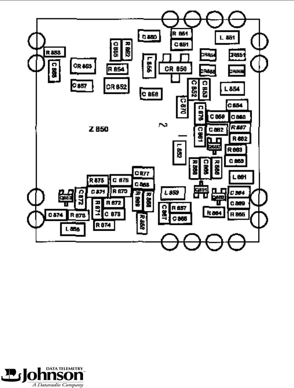
SCHEMATICS AND COMPONENT LAYOUTS
8-2
Part No. 001-3474-002
Figure 8-1 VCO COMPONENT LAYOUT (COMPONENT SIDE VIEW)

SCHEMATICS AND COMPONENT LAYOUTS
8-3
Part No. 001-3474-002
Figure 8-2 TRANSCEIVER COMPONENT LAYOUT (COMPONENT SIDE VIEW)
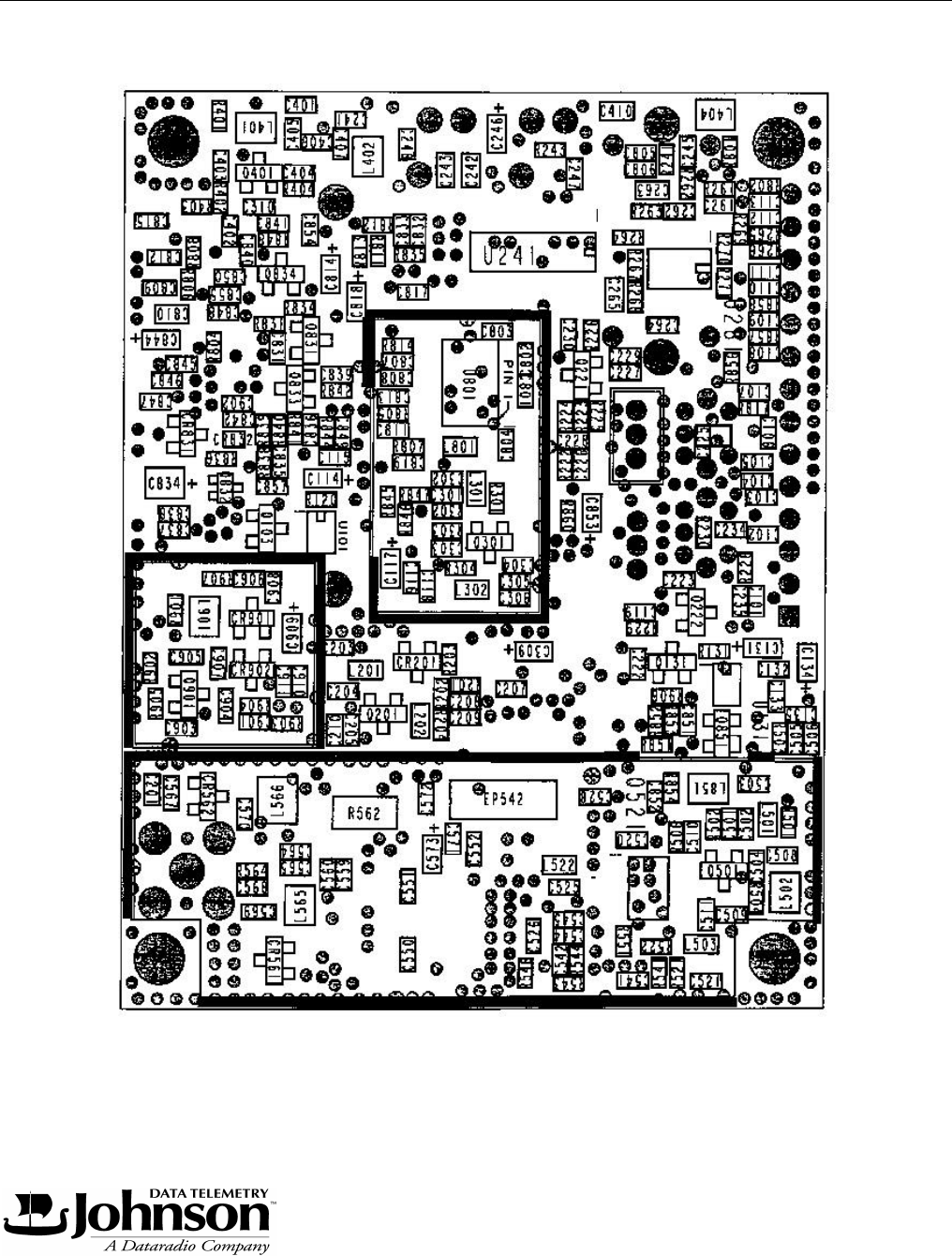
SCHEMATICS AND COMPONENT LAYOUTS
8-4
Part No. 001-3474-002
Figure 8-3 TRANSCEIVER COMPONENT LAYOUT (OPPOSITE COMPONENT SIDE VIEW)

SCHEMATICS AND COMPONENT LAYOUTS
8-5
Part No. 001-3474-002
Figure 8-4 DM-3474 SCHEMATIC
Company Confidential
Copyright 1998 Johnson Data Telemetry Corporation

SCHEMATICS AND COMPONENT LAYOUTS
8-6
Part No. 001-3474-002
This page intentionally left blank.