Galaxy Tracking Systems VTRAKH450 UHF-FM VehicleTracking Unit User Manual Cover
Galaxy Tracking Systems L.L.C. UHF-FM VehicleTracking Unit Cover
UserManual.wiki
>
Galaxy Tracking Systems
>
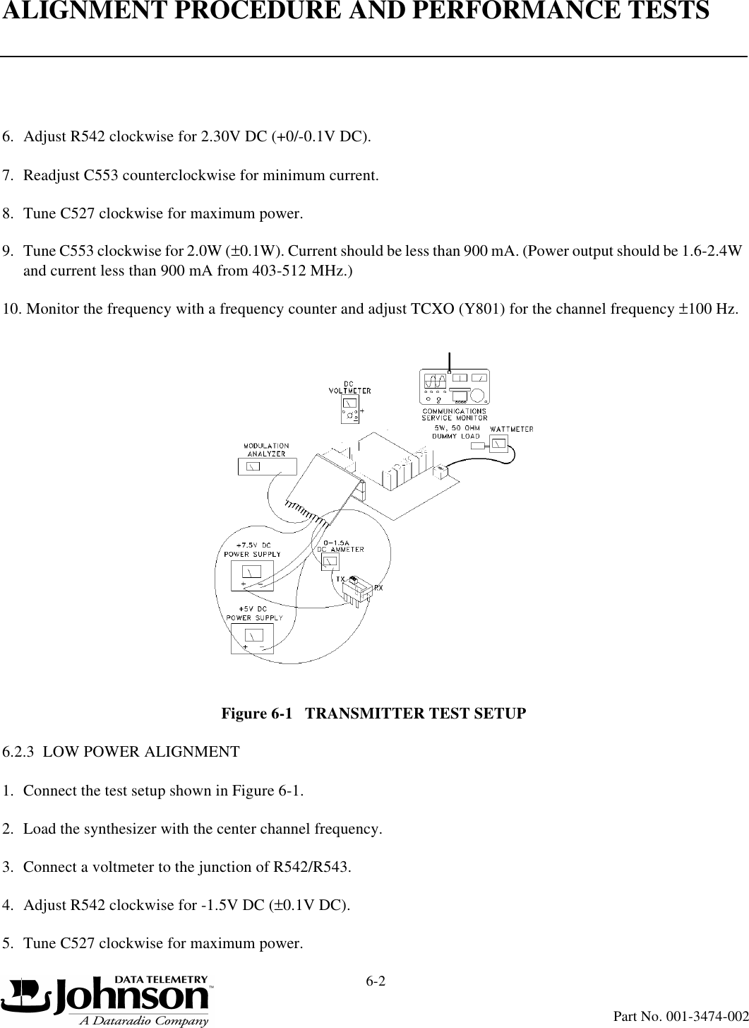
VTRAKH450 User Manual
>
Service Manual
Contents
1.
Users Manual1
2.
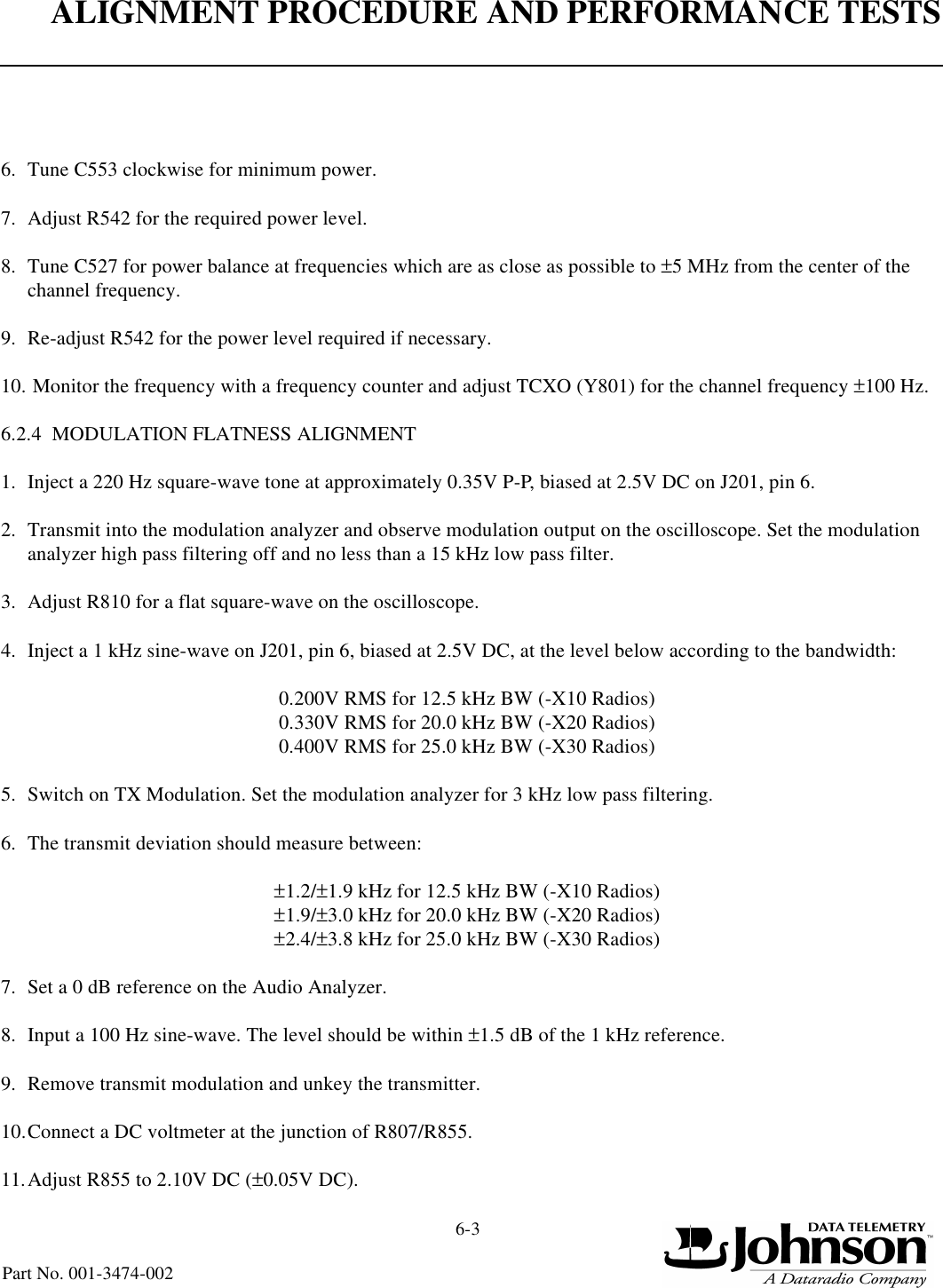
Users Manual2
3.
Service Manual
Service Manual
Navigation menu
Upload a User Manual
Namespaces
Wiki Guide
HTML
PDF
Info
Views
User Manual
Discussion / Help
Navigation

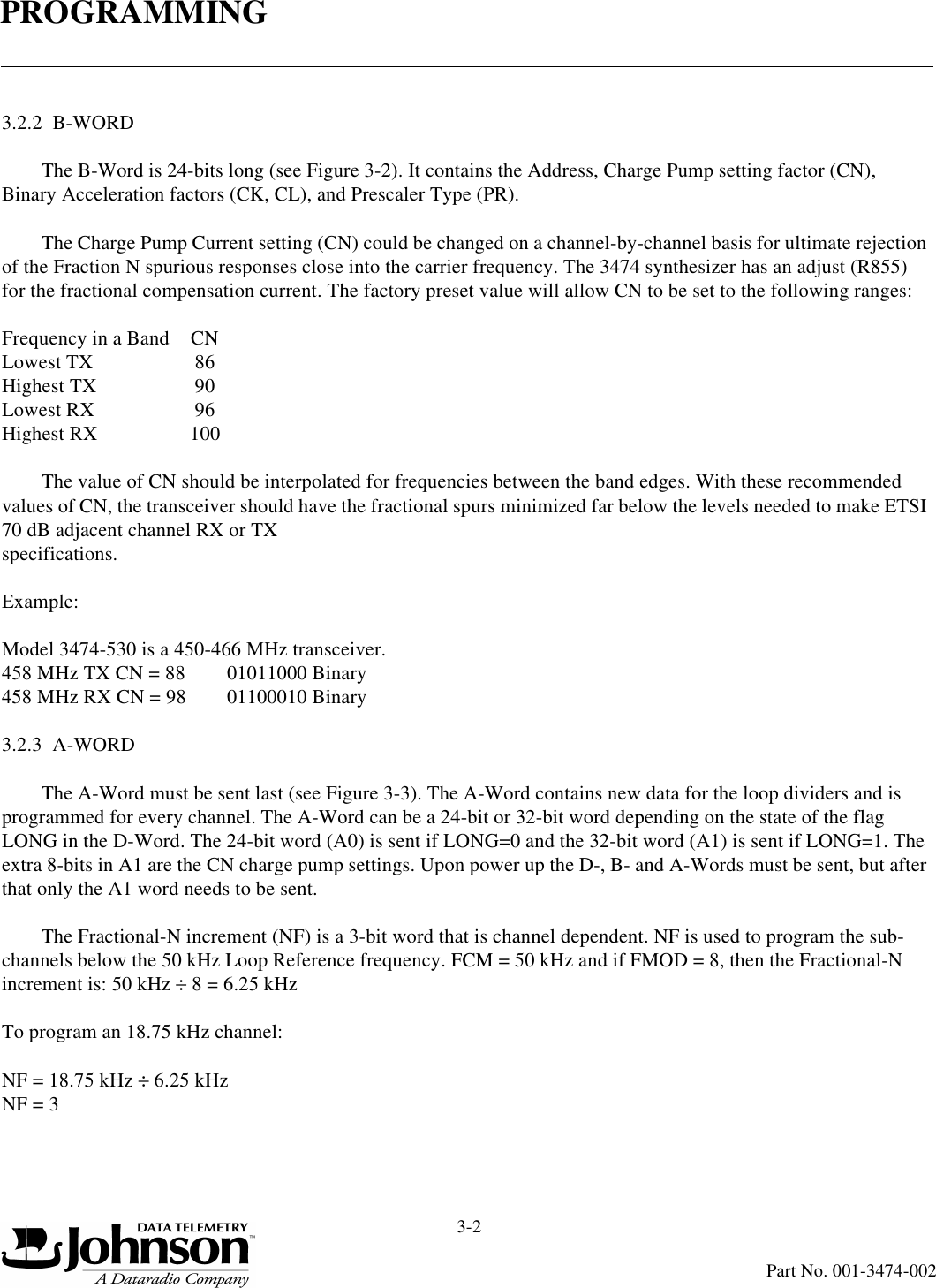
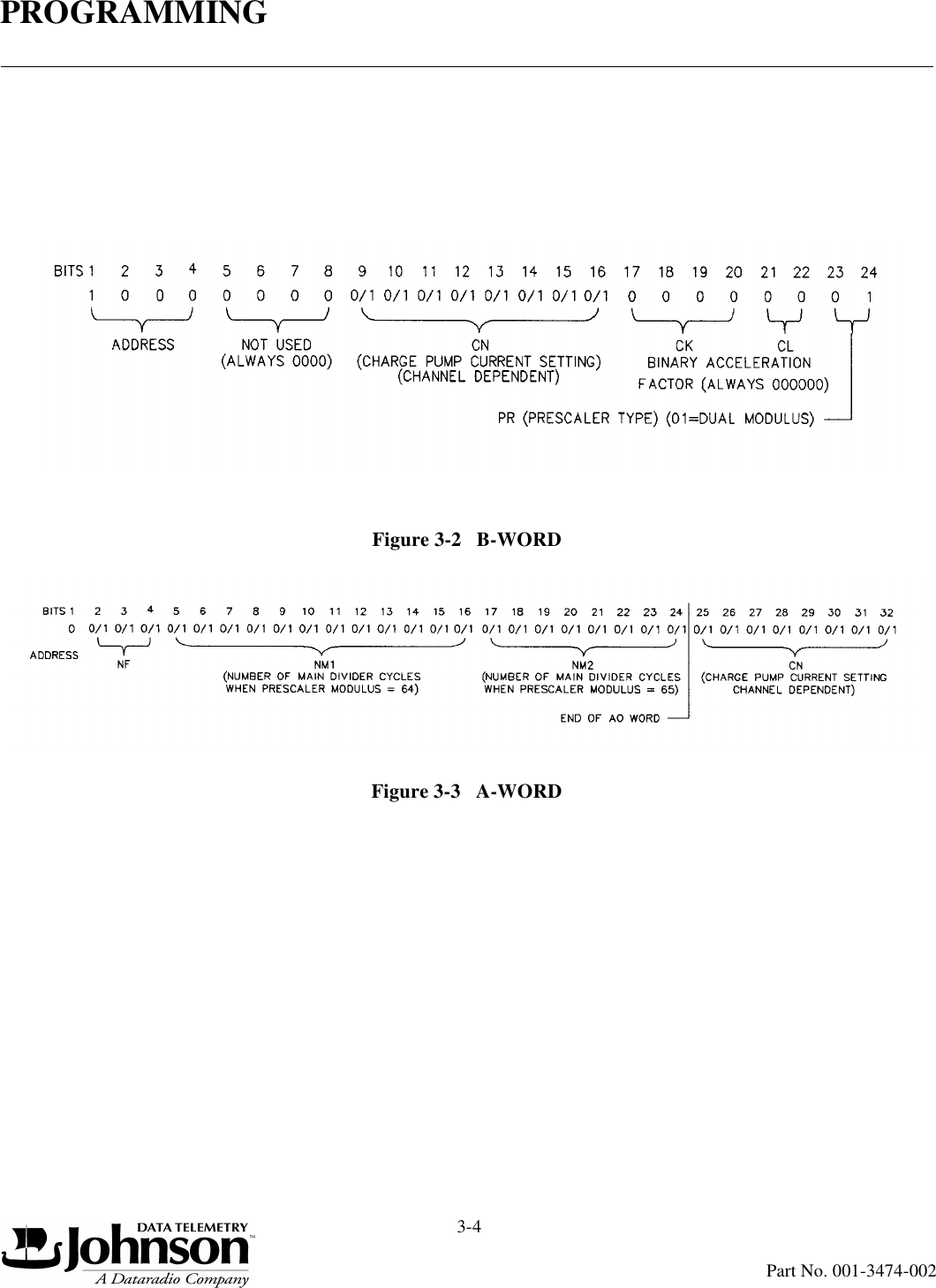
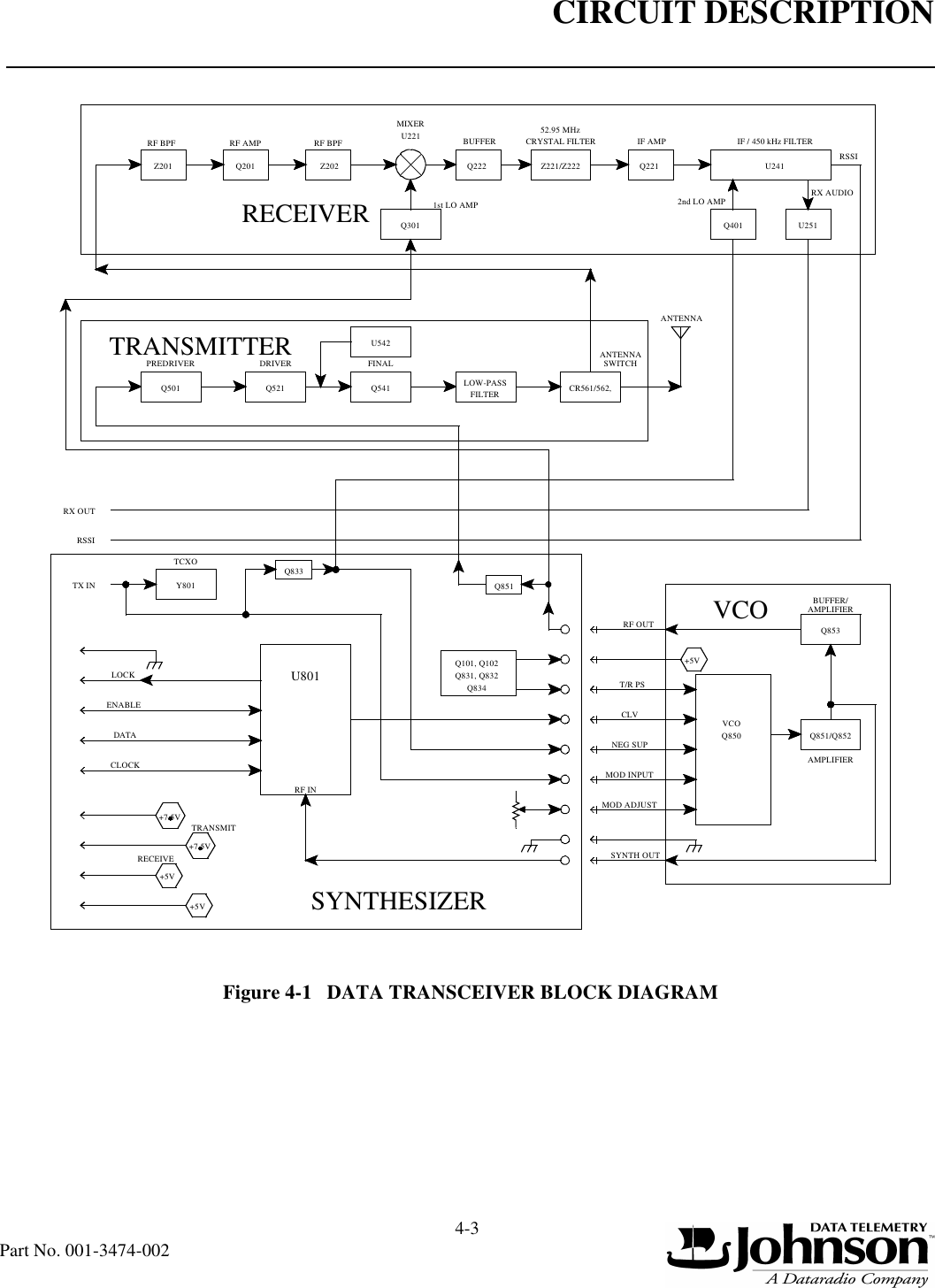
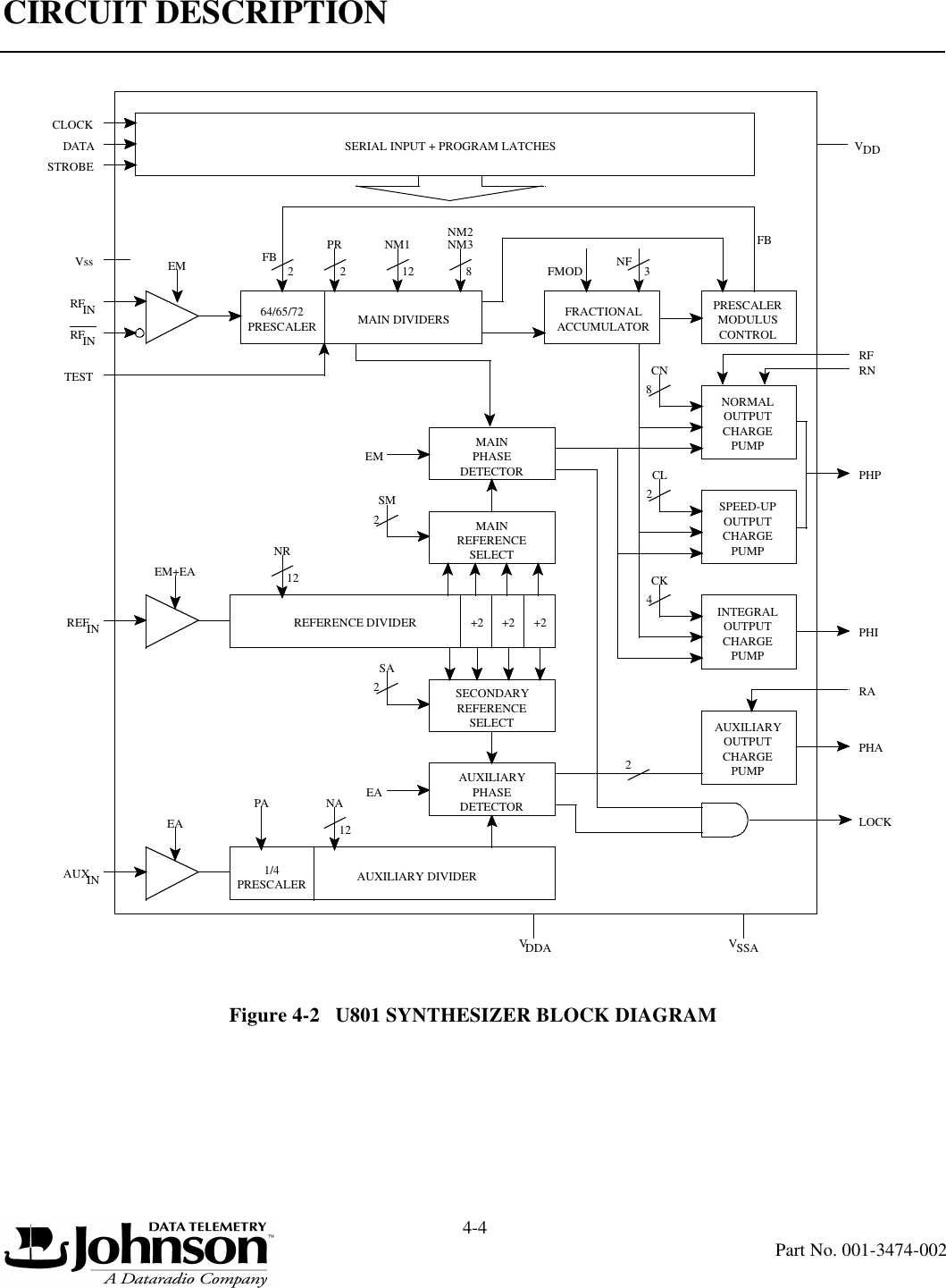
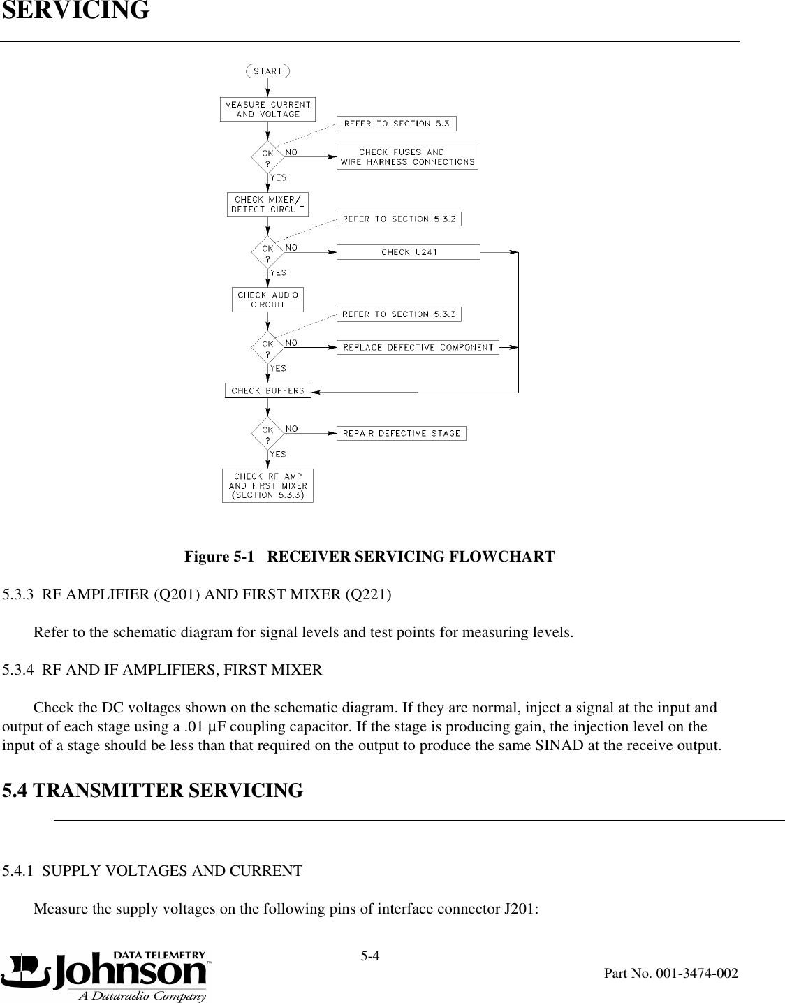
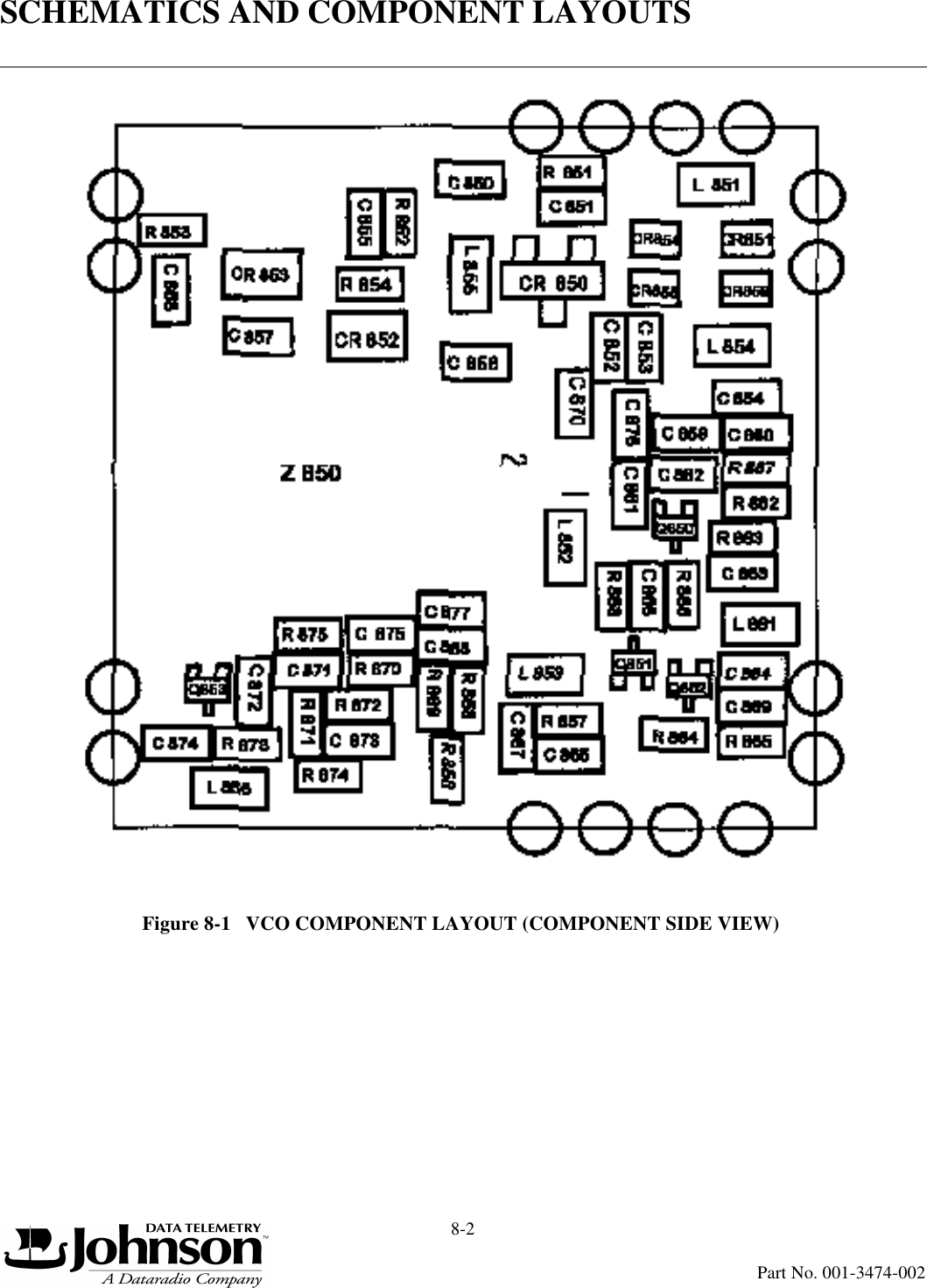
![PROGRAMMING3-3Part No. 001-3474-002NM1 and NM2 are calculated as follows:N = (NM1 + 2) x 64 + NM2 x 65 Where: N = total division ratioNM1 = Number of main divider cycles when prescaler modulus equals 64NM2 = Number of main divider cycles when prescaler modulus equals 65Example:Calculate NM1 and NM2 to Receive 454.500 MHz.LO = 454.5 + 52.95 = 507.45 MHz (52.95 MHz IF with High Side Injection)N = RX LO ÷ FCM = 507.45 ÷ 0.05 = 10149 (FMC = Loop Reference Frequency)NM2 = 64 x FRAC [N ÷ 64] = 64 x FRAC [10149 ÷ 64]= 64 x 0.57813= 37NM1 = INTEGER [N ÷ 64] - 2 - NM2= 158 - 2 - 37= 119Figure 3-1 D-WORD](https://usermanual.wiki/Galaxy-Tracking-Systems/VTRAKH450.Service-Manual/User-Guide-78930-Page-19.png)