Gemalto M2M ELS31-VA CAT 1 LTE Module User Manual hid elsx1 va
Gemalto M2M GmbH CAT 1 LTE Module hid elsx1 va
UserManual.wiki
>
Gemalto M2M
>
ELS31-VA User Manual
>
user manual
Contents
1.
user manual
2.
User Manual
user manual
Navigation menu
Upload a User Manual
Namespaces
Wiki Guide
HTML
PDF
Info
Views
User Manual
Discussion / Help
Navigation
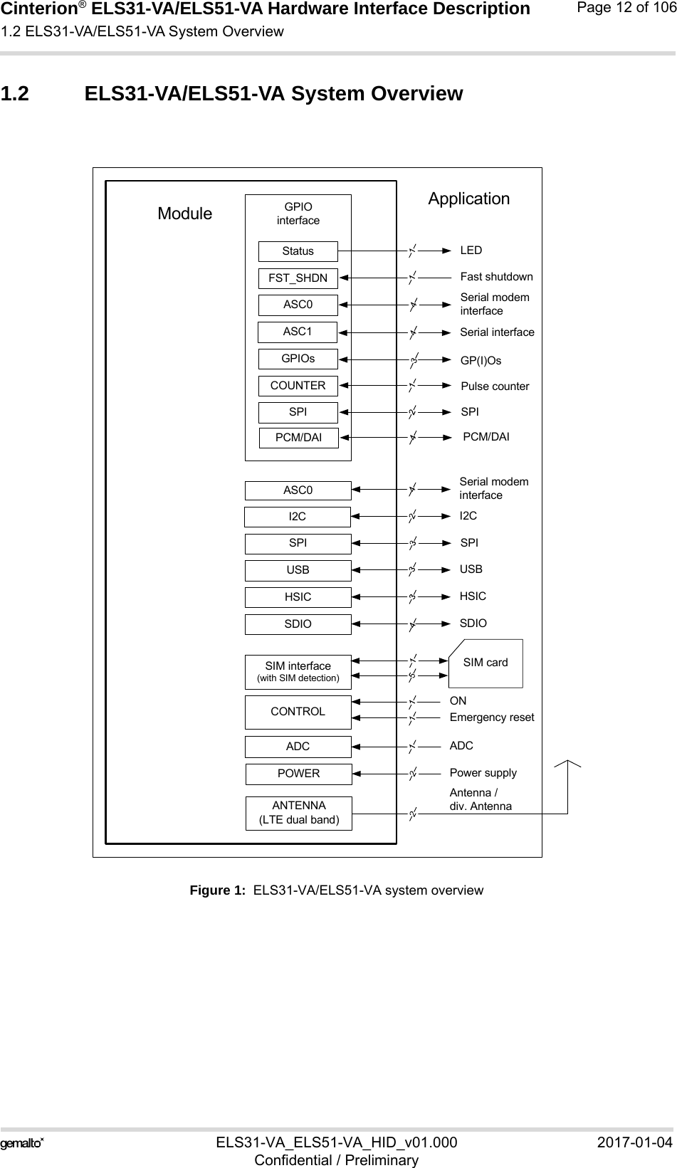
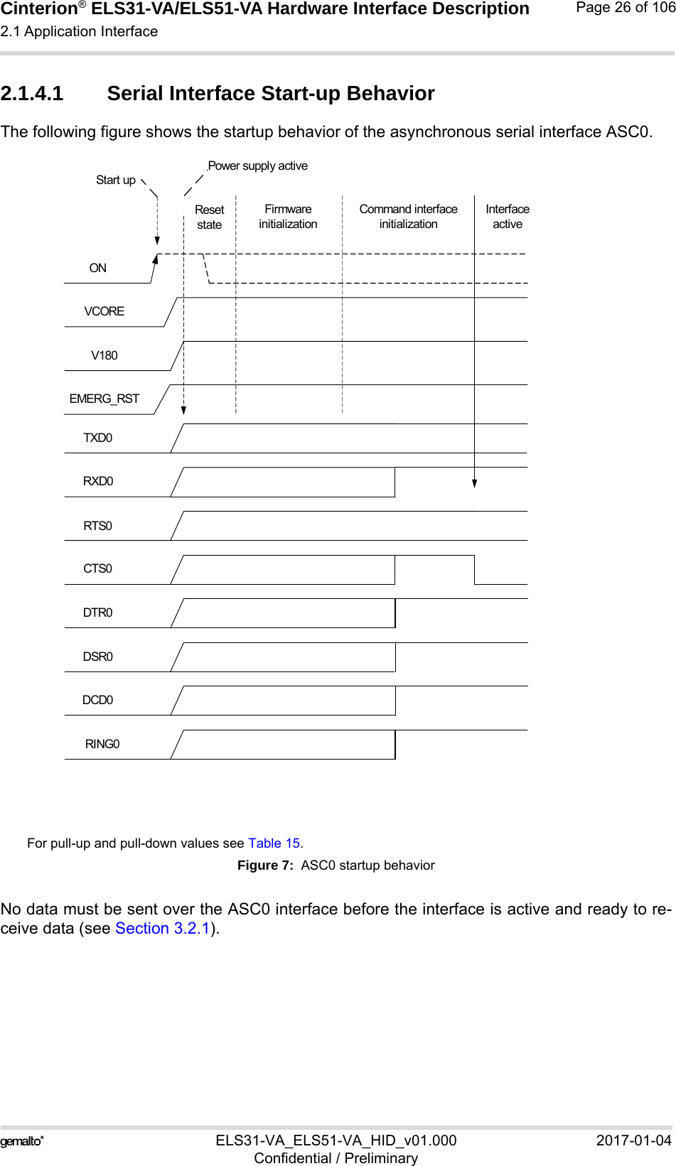
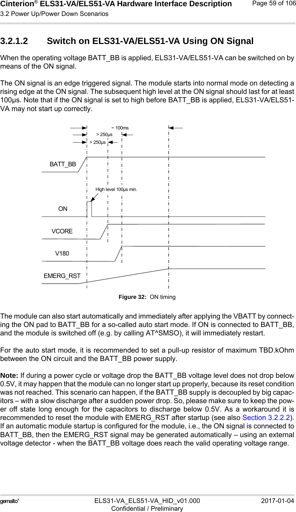
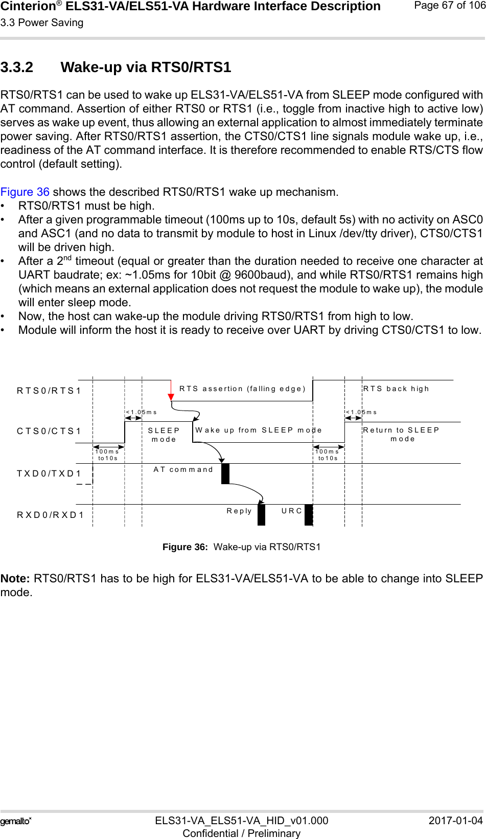
![Cinterion® ELS31-VA/ELS51-VA Hardware Interface Description1.1 Key Features at a Glance13ELS31-VA_ELS51-VA_HID_v01.000 2017-01-04Confidential / PreliminaryPage 10 of 106InterfacesModule interface Surface mount device with solderable connection pads (SMT application interface). Land grid array (LGA) technology ensures high solder joint reli-ability and allows the use of an optional module mounting socket.For more information on how to integrate SMT modules see also [4]. This application note comprises chapters on module mounting and application layout issues as well as on SMT application development equipment.USB USB 2.0 High Speed (480Mbit/s) device interface, Full Speed (12Mbit/s)compliant2 serial interfaces ASC0:• 8-wire modem interface with status and control lines, unbalanced, asyn-chronous• Default baud rate: 115,200 baud• Adjustable baud rates: 4,800 to 921,600, no autobauding support• Supports RTS0/CTS0 hardware flow control. • Indication of incoming data/SMS on RING0 (can be used to wake uphost from power down modes)ASC1 (shared with GPIO lines):• 4-wire, unbalanced asynchronous interface• Default baud rate: 115,200 baud• Adjustable baud rates: 4,800bps to 921,600bps• Supports RTS1/CTS1 hardware flow controlUICC interface Supported SIM/USIM cards: 3V, 1.8VEmbedded UICC Module is prepared for an embedded UICCGPIO interface 20 pads of the application interface programmable as GPIO pads (17) or GPO pads (3):GP(I)Os can be configured as COUNTER, FST_SHDN, ASC0, ASC1, SPI, and DAI signal linesProgramming is done via AT commandsI2C interface Supports I2C serial interfaceSPI interface Supports SPI interfaceSDIO ELS51-VA only:4 wire interface.HSIC ELS51-VA only:High Speed Interchip Communication interface. ADC Analog-to-Digital Converter with one unbalanced analog input.Digitial audio interface 4 GPIO lines can be configured as PCM/I2S lines for VoLTE communica-tion.Antenna interface pads 50Ω LTE main antenna, 50LTE diversity antennaFeature Implementation](https://usermanual.wiki/Gemalto-M2M/ELS31-VA.user-manual/User-Guide-3274854-Page-10.png)
![Cinterion® ELS31-VA/ELS51-VA Hardware Interface Description2.1 Application Interface56ELS31-VA_ELS51-VA_HID_v01.000 2017-01-04Confidential / PreliminaryPage 24 of 1062.1.3.2 Reducing Power ConsumptionWhile a USB connection is active, the module will never switch into SLEEP mode. Only if the USB interface is in Suspended state or Detached (i.e., VUSB_IN = 0) is the module able to switch into SLEEP mode thereby saving power. There are two possibilities to enable power re-duction mechanisms:• Recommended implementation of USB Suspend/Resume/Remote Wakeup:The USB host should be able to bring its USB interface into the Suspended state asdescribed in the “Universal Serial Bus Specification Revision 2.0“1. For this functionality towork, the VUSB_IN line should always be kept enabled. On incoming calls and other eventsELS31-VA/ELS51-VA will then generate a Remote Wakeup request to resume the USBhost controller.See also [5] (USB Specification Revision 2.0, Section 10.2.7, p.282):"If USB System wishes to place the bus in the Suspended state, it commands the Host Con-troller to stop all bus traffic, including SOFs. This causes all USB devices to enter the Sus-pended state. In this state, the USB System may enable the Host Controller to respond tobus wakeup events. This allows the Host Controller to respond to bus wakeup signaling torestart the host system."• Implementation for legacy USB applications not supporting USB Suspend/Resume:As an alternative to the regular USB suspend and resume mechanism it is possible toemploy the RING0 line to wake up the host application in case of incoming calls or eventssignalized by URCs while the USB interface is in Detached state (i.e., VUSB_IN = 0). Everywakeup event will force a new USB enumeration. Therefore, the external application has tocarefully consider the enumeration timings to avoid loosing any signalled events. For detailson this host wakeup functionality see Section 2.1.16.3. Note: Existing data connections will not be disconnected even if the USB interface is in de-tached state. URCs will be queued during detached state, but may be signaled to the host via host wakeup line RING0.1. The specification is ready for download on http://www.usb.org/developers/docs/](https://usermanual.wiki/Gemalto-M2M/ELS31-VA.user-manual/User-Guide-3274854-Page-24.png)
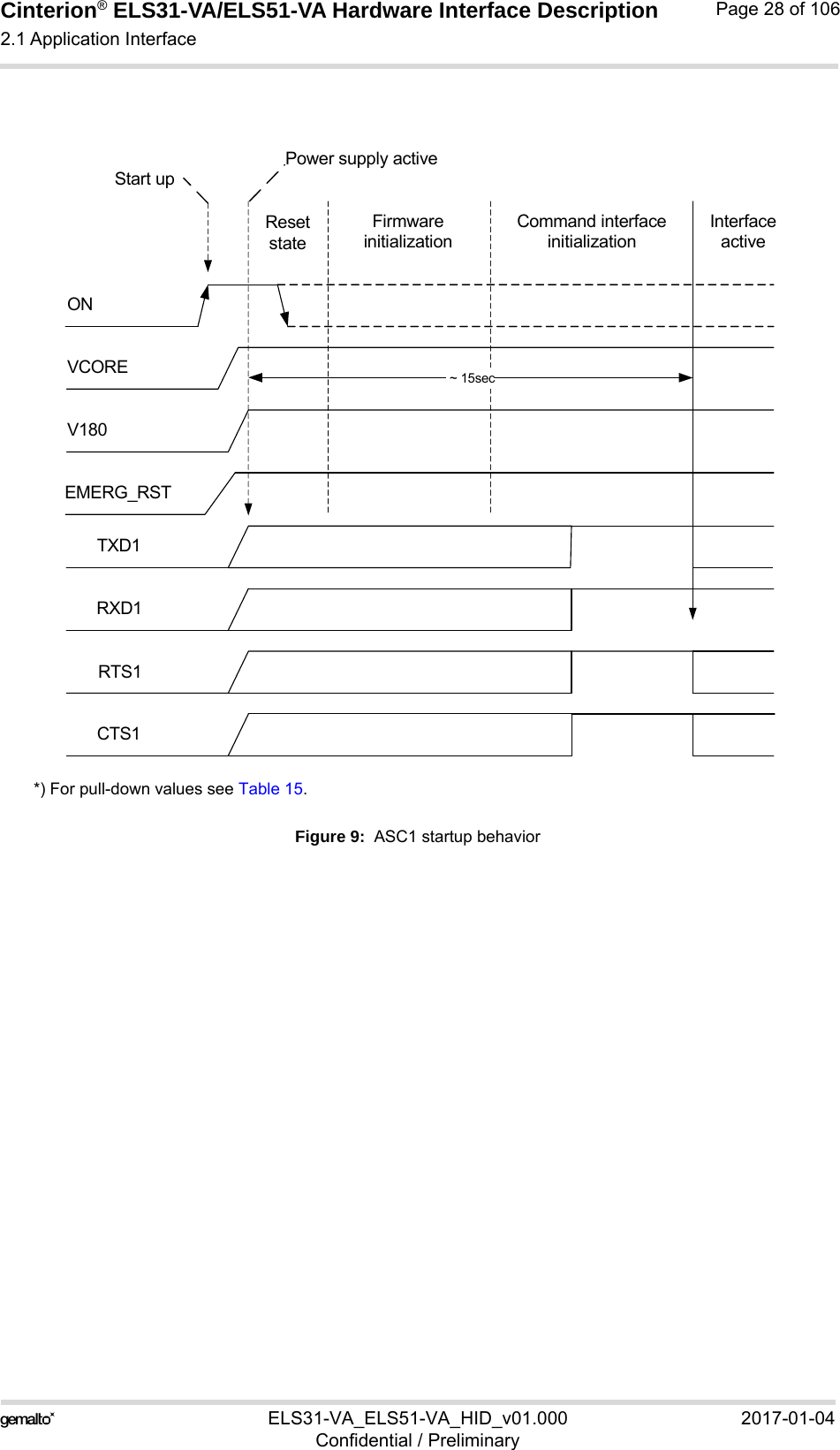
![Cinterion® ELS31-VA/ELS51-VA Hardware Interface Description2.1 Application Interface56ELS31-VA_ELS51-VA_HID_v01.000 2017-01-04Confidential / PreliminaryPage 27 of 1062.1.5 Serial Interface ASC1ELS31-VA/ELS51-VA provides a 4-wire unbalanced, asynchronous modem interface ASC1conforming to ITU-T V.24 protocol DCE signaling. The electrical characteristics do not complywith ITU-T V.28. The significant levels are 0V (for low data bit or active state) and 1.8V (for highdata bit or inactive state). For electrical characteristics please refer to Table 2. For an illustra-tion of the interface line’s startup behavior see Figure 9. ASC1 can only be used as data inter-face.The ASC1 interface lines are originally available as GPIO lines. If configured as ASC1 lines, the GPIO lines are assigned as follows: GPIO16 --> RXD1, GPIO17 --> TXD1, GPIO18 --> RTS1 and GPIO19 --> CTS1. Configuration is done by AT command (see [1]: AT^SCFG). The configuration is non-volatile and becomes active after a module restart.ELS51-VA is designed for use as a DCE. Based on the conventions for DCE-DTE connectionsit communicates with the customer application (DTE) using the following signals:• Port TXD @ application sends data to module’s TXD1 signal line• Port RXD @ application receives data from the module’s RXD1 signal lineFigure 8: Serial interface ASC1Features• Includes only the data lines TXD1 and RXD1 plus RTS1 and CTS1 for hardware hand-shake. • On ASC1 no RING line is available.• Configured for 8 data bits, no parity and 1 or 2 stop bits.• ASC1 can be operated at fixed bit rates from 4800 bps to 921600 bps.• Supports RTS1/CTS1 hardware flow control. Communication is possible by using only RXDand TXD lines, if RTS1 is pulled low.• Wake up from SLEEP mode by RTS0 activation (high to low transition; see Section 3.3.2).AT commands for signaling are not supported on ASC1 interface. ASC1 is intended only fordata transfer in a Linux environment.The following figure shows the startup behavior of the asynchronous serial interface ASC1.](https://usermanual.wiki/Gemalto-M2M/ELS31-VA.user-manual/User-Guide-3274854-Page-27.png)
![Cinterion® ELS31-VA/ELS51-VA Hardware Interface Description2.1 Application Interface56ELS31-VA_ELS51-VA_HID_v01.000 2017-01-04Confidential / PreliminaryPage 31 of 1062.1.7 Digital Audio InterfaceELS31-VA/ELS51-VA supports a digital audio interface that can be employed either as pulse code modulation interface (see Section 2.1.8) or as inter IC sound interface (see Section 2.1.9). Operation of these interface variants is mutually exclusive, and can be configured by AT com-mand (see [1])). Default setting is pulse code modulation.2.1.8 Pulse Code Modulation Interface (PCM)Note: ELS31-VA/ELS51-VA's PCM interface is reserved for future use. Usage as digital audio interface is currently not supported.ELS31-VA/ELS51-VA's PCM interface can be used to connect audio devices capable of pulse code modulation. The PCM functionality is limited to the use of covers the use of narrowband codecs with 8kHz sample rate and wideband codecs with 16kHz sample rate onlyas well. Con-figured for wideband the The PCM interface runs at 16 kHz sample rate (62.5µs frame length), while the signal processing maintains this rate in a wideband AMR call or samples automati-cally down to 8kHz in a narrowband call. Therefore, the PCM sample rate is independent of the audio bandwidth of the call.The PCM interface has the following implementation:•Slave mode• Short frame synchronization, long frame synchronization• 8kHz and 16kHz sample rate• 256kHz, 512kHz, 2048kHz bit clock at 8kHz sample rate• 256kHz, 512kHz, 1024kHz, 4096kHz bit clock at 16kHz sample rateFor the PCM configuration the AT^SAIC command parameters <clock>, <mode>, <frame_-mode>, <ext_clk_mode> and <sample_rate> (see [1]) cannot be configured in any combina-tion. The following notes, must be considered while configuring the PCM interface:ELS31-VA/ELS51-VA’s digital audio interface can only be operated in slave mode. Therefore, the <mode> parameter must be set to <1>, and the <ext_clk_mode> be set to not permanent resp. off. Further, while in slave mode the <clock>, <frame_mode> and <sample_rate> must be set according to the characteristics of the external master. There is no automatic detection of the received clock frequency, frame length and sample rate.Four GPIOs can be configured by AT command as PCM signals: GPIO20 --> PCM_I2S_OUT, GPIO21--> PCM_I2S_IN, GPIO22 --> PCM_I2S_FSC and GPIO23 --> PCM_I2S_CLK. The setting is non-volatile and becomes active after a module restart (see also [1]).Table 5 describes the available DAI/PCM lines at the digital audio interface. For electrical de-tails see Section 2.1.2.](https://usermanual.wiki/Gemalto-M2M/ELS31-VA.user-manual/User-Guide-3274854-Page-31.png)
![Cinterion® ELS31-VA/ELS51-VA Hardware Interface Description2.1 Application Interface56ELS31-VA_ELS51-VA_HID_v01.000 2017-01-04Confidential / PreliminaryPage 32 of 106Note: PCM data is always formatted as 16-bit uncompressed two’s complement. Also, all PCM data and frame synchronization signals are written to the PCM bus on the rising clock edge and read on the falling edge.The timing of a PCM short frame is shown in Figure 11.Figure 11: PCM timing short frame (4096KHz, 16kHz sample rate)Configured to short frame synchronization, the pulse on PCM_I2S_FSC should be one clock period wide and occur one clock before the data, using long frame the pulse should have a duty cycle of 50% starting with the first data bit. Characteristics of Audio ModesELS31-VA/ELS51-VA has various audio modes selectable with AT^SNFS (for details on AT^SNFS see [1]).Audio mode 1 with its default settings is used for type approval with the Votronic handset via the DSB75 codec adapter. The handset is adjusted for the type 3.2 low-leakage ear simulator for narrowband and wideband calls. The other modes are customer specific modes, and can as such be prepared for specific re-quirements. Table 5: Overview of PCM pin functionsSignal name on B2B connectorSMT application interfaceSignal configuration inactiveSignal direction: SlaveDescriptionPCM_I2S_OUT PD O PCM data from ELS31-VA/ELS51-VA to external codecPCM_I2S_IN PD I PCM data from external codec to ELS31-VA/ELS51-VA PCM_I2S_FSC PD I Frame synchronization signal from external codecPCM_I2S_CLK PD I Bit clock from external codecMSBMSBLSBLSB14 1314 1311121222MSBMSB62.5 µsPCM_I2S_CLKPCM_I2S_FSCPCM_I2S_OUTPCM_I2S_IN](https://usermanual.wiki/Gemalto-M2M/ELS31-VA.user-manual/User-Guide-3274854-Page-32.png)
![Cinterion® ELS31-VA/ELS51-VA Hardware Interface Description2.1 Application Interface56ELS31-VA_ELS51-VA_HID_v01.000 2017-01-04Confidential / PreliminaryPage 33 of 1062.1.9 Inter IC Sound Interface (I2S)The I2S Interface is a standardized bidirectional I2S ("Inter-IC Sound Interface") based digital audio interface for transmission of mono voice signals for telephony services.The I2S interface can be enabled and configured using the AT command AT^SAIC (see [1]). An activation is possible only out of call and out of tone presentation. The I2S properties and capabilities comply with the requirements laid out in the Phillips I2S Bus Specifications, revised June 5, 1996.The I2S interface has the following characteristics:• Bit clock mode: Slave, requires external master clock input • Sampling rate: 8KHz (narrowband), 16KHz (wideband)• 256kHz bit clock at 8kHz sample rate• 512kHz bit clock at 16kHz sample rate• Frame length: 32 bit stereo voice signal (16 bit word length)The digital audio interface lines available for the PCM interface are also available for the I2S interface. In I2S mode they have the same electrical characteristics. Table 6 lists the available I2S interface signals, Figure 12 shows the I2S timing. Figure 12: I2S timing (slave mode)Table 6: Overview of I2S pin functionsSignal name on SMT application interfaceSignal configuration inactiveSignal direction: SlaveDescriptionPCM_I2S_OUT PD O I2S data from ELS31-VA/ELS51-VA to external codecPCM_I2S_IN PD I I2S data from external codec to ELS31-VA/ELS51-VA PCM_I2S_FSC PD I Frame synchronization signal from external codec Word alignment (WS)PCM_I2S_CLK PD I Bit clock from external codecPCM_I2S_CLKPCM_I2S_OUTPCM_I2S_INPCM_I2S_FSCMSBMSBLSBLSB14 1314 1311121222MSBMSB125 µs](https://usermanual.wiki/Gemalto-M2M/ELS31-VA.user-manual/User-Guide-3274854-Page-33.png)
![Cinterion® ELS31-VA/ELS51-VA Hardware Interface Description2.1 Application Interface56ELS31-VA_ELS51-VA_HID_v01.000 2017-01-04Confidential / PreliminaryPage 34 of 1062.1.10 GPIO InterfaceELS31-VA/ELS51-VA offers a GPIO interface with 17 GPIO and 3 GPO lines. The lines areshared with other interfaces or functions: Fast shutdown (see Section 2.1.16.4), status LED(see Section 2.1.16.1), a pulse counter (see Section 2.1.13), ASC0 (see Section 2.1.4), ASC1(see Section 2.1.5), SPI (see Section 2.1.12), HSIC (see Section 2.1.14), and digital audio in-terface (DAI; see Section 2.1.7).The following table shows the configuration variants for the GPIO pads. All variants are mutu-ally exclusive, i.e. a pad configured for instance as Status LED is locked for alternative usage.After startup, the above mentioned alternative GPIO line assignments can be configured usingAT commands (see [1]). The configuration is non-volatile and available after module restart.Notes:• GPO5, GPO23 and GPO26 are GPOs only.Table 7: GPIO lines and possible alternative assignmentGPIO Fast Shutdown Status LED Pulse Counter ASC0 ASC1 SPI HSIC PCMGPIO1 DTR0GPIO2 DCD0GPIO3 DSR0GPIO4 FST_SHDNGPO5 LEDGPIO6GPIO7GPIO8 COUNTERGPIO16 RXD1 AP_WAKEUPGPIO17 TXD1 HOST_ACTIVEGPIO18 RTS1 CP_WAKEUPGPIO19 CTS1 SUSPENDGPIO20 PCM_I2S_OUTGPIO21 PCM_I2S_INGPIO22 PCM_I2S_FSCGPO23 PCM_I2S_CLKGPIO24 RING0GPIO25GPO26 SPI_CS1GPIO27 SPI_CS2](https://usermanual.wiki/Gemalto-M2M/ELS31-VA.user-manual/User-Guide-3274854-Page-34.png)
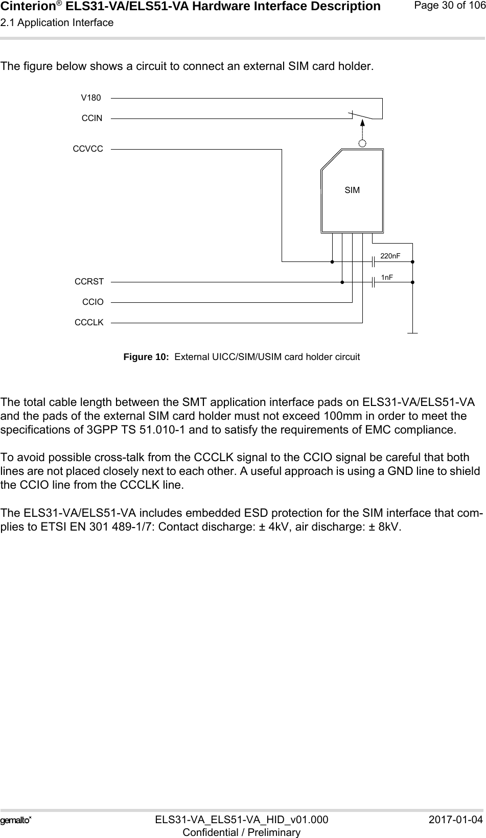
![Cinterion® ELS31-VA/ELS51-VA Hardware Interface Description2.1 Application Interface56ELS31-VA_ELS51-VA_HID_v01.000 2017-01-04Confidential / PreliminaryPage 36 of 1062.1.11 I2C InterfaceI2C is a serial, 8-bit oriented data transfer bus for bit rates up to 100kbps. It consists of two lines,the serial data line I2CDAT and the serial clock line I2CCLK. The module acts as a single mas-ter device, e.g. the clock I2CCLK is driven by the module. I2CDAT is a bi-directional line. Eachdevice connected to the bus is software addressable by a unique 7-bit address, and simplemaster/slave relationships exist at all times. The module operates as master-transmitter or asmaster-receiver. The customer application transmits or receives data only on request of themodule.To configure and activate the I2C bus use the AT^SSPI command. Detailed information on theAT^SSPI command as well explanations on the protocol and syntax required for data transmis-sion can be found in [1].The I2C interface can be powered via the V180 line of ELS31-VA/ELS51-VA. If connected tothe V180 line, the I2C interface will properly shut down when the module enters the PowerDown mode.In the application I2CDAT and I2CCLK lines need to be connected to a positive supply voltagevia a pull-up resistor. For electrical characteristics please refer to Table 2.Figure 14: I2C interface connected to V180Note: Good care should be taken when creating the PCB layout of the host application: Thetraces of I2CCLK and I2CDAT should be equal in length and as short as possible.I2CCLKI2CDATGNDI2CCLKI2CDATGNDModule ApplicationV180R pull upR pull upR pull upR pull up](https://usermanual.wiki/Gemalto-M2M/ELS31-VA.user-manual/User-Guide-3274854-Page-36.png)
![Cinterion® ELS31-VA/ELS51-VA Hardware Interface Description2.1 Application Interface56ELS31-VA_ELS51-VA_HID_v01.000 2017-01-04Confidential / PreliminaryPage 38 of 1062.1.12 SPI InterfaceThe ELS31-VA/ELS51-VA GPIO interface lines can be configured as Serial Peripheral Inter-face (SPI). The SPI is a synchronous serial interface for control and data transfer betweenELS31-VA/ELS51-VA and the external application. Only one application can be connected tothe SPI and the interface supports only master mode. The transmission rates are up to 6.5Mbit/s. The SPI interface comprises the two data lines SPI_MOSI and SPI_MISO, the clock lineSPI_CLK a well as the chip select lines SPI_CS1 and SPI_CS2.These two GPIO lines can be configured as SPI interface signals as follows: GPO26 --> SPI_CS1 and GPIO27 --> SPI_CS2. The configuration is done by AT command (see [1]). It is non-volatile and becomes active after a module restart.To configure and activate the SPI interface use the AT^SSPI command. Detailed informationon the AT^SSPI command as well explanations on the SPI modes required for data transmis-sion can be found in [1].In general, SPI supports four operation modes. The modes are different in clock phase andclock polarity. The module’s SPI mode can be configured by using the AT command AT^SSPI.Make sure the module and the connected slave device works with the same SPI mode.Figure 16 shows the characteristics of the four SPI modes. The SPI modes 0 and 3 are the mostcommon used modes. For electrical characteristics please refer to Table 2.Figure 16: Characteristics of SPI modesSPI MODE 0 SPI MODE 1SPI MODE 2 SPI MODE 3Clock phaseClock polaritySPI_CSSPI_MOSISPI_CLKSPI_MISOSPI_CSSPI_MOSISPI_CLKSPI_MISOSPI_CSSPI_MOSISPI_CLKSPI_MISOSPI_CSSPI_MOSISPI_CLKSPI_MISOSample SampleSample Sample](https://usermanual.wiki/Gemalto-M2M/ELS31-VA.user-manual/User-Guide-3274854-Page-38.png)
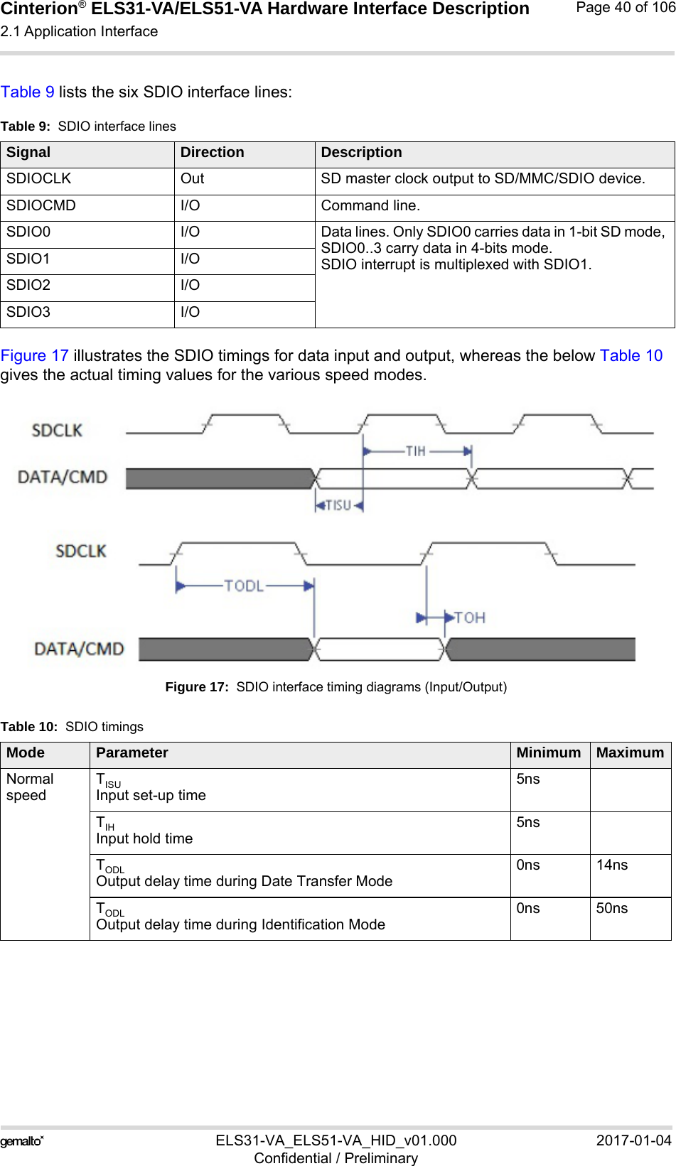
![Cinterion® ELS31-VA/ELS51-VA Hardware Interface Description2.1 Application Interface56ELS31-VA_ELS51-VA_HID_v01.000 2017-01-04Confidential / PreliminaryPage 39 of 1062.1.13 Pulse CounterThe GPIO8 line can be configured as pulse counter line COUNTER (for GPIOs see Section2.1.10). The pulse counter interface can be used, for example, as a clock - it is designed tomeasure signals from 0 to 1000 pulses per second. Note that the pulse counter works in batch-es of 8 pulses, i.e., the URC indicates the number of pulses counted in batches of 8 pulses. Formore information on how to use this feature see [1].2.1.14 HSIC Interface (ELS51-VA Only)The (USB) High Speed Inter Chip (HSIC) interface can be used between the module and an external application processor, and is compliant to the High Speed USB 2.0 interface with 480Mbit/s. The maximum distance between module processor and external application proces-sor should not exceed 100mm.The HSIC interface comprises two signal lines (strobe - HSIC_STRB - and data - HSIC_DATA) used in a source synchronous serial interface with a 240MHz clock to provide a 480Mbps USB interface. The HSIC_STRB and HSIC_DATA lines are high-speed signals and should be rout-ed as 50Ohm impedance traces. The trace length of these signals should be balanced to min-imize timing skew and be no longer than 100mm.The HSIC interface implementation complies with the USB HSIC standard “High-Speed Inter-Chip USB Electrical Specification”, Version 1, September 23, 20071.2.1.15 SDIO Interface (ELS51-VA Only)The Secure Digital Input Output (SDIO) interface can be used to for instance connect an SD card. The SDIO interface has the following features:1. The USB specifications are ready for download on http://www.usb.org/developers/docs/usb20_docs/Table 8: SDIO interface featuresFeature Description/ValueInterface Type SDIO/SD1 (1 data line), SDIO/SD4 (4 data lines), MMC4 (4 data lines)Voltage 1.8 VDMA Mode SDMA / ADMA1 / ADMA2Number of SLOTs 1Implement DDR mode YesCard inserted status YesSDIOCLK frequency Default Mode: 23 MHz maximumHigh Speed Mode: 46 MHz maximumUHS-I Mode: 92 MHzMax block length 2048 bytesSDIO interrupt support Yes, support SDIO/SD1, SDIO/SD4 mode interrupts](https://usermanual.wiki/Gemalto-M2M/ELS31-VA.user-manual/User-Guide-3274854-Page-39.png)
![Cinterion® ELS31-VA/ELS51-VA Hardware Interface Description2.1 Application Interface56ELS31-VA_ELS51-VA_HID_v01.000 2017-01-04Confidential / PreliminaryPage 43 of 1062.1.16.2 Power Indication CircuitIn Power Down mode the maximum voltage at any digital or analog interface line must not ex-ceed +0.3V (see also Section 2.1.2.1). Exceeding this limit for any length of time might causepermanent damage to the module. It is therefore recommended to implement a power indication signal that reports the module’spower state and shows whether it is active or in Power Down mode. While the module is inPower Down mode all signals with a high level from an external application need to be set tolow state or high impedance state. The sample power indication circuit illustrated in Figure 19denotes the module’s active state with a low signal and the module’s Power Down mode witha high signal or high impedance state.Figure 19: Power indication circuit2.1.16.3 Host WakeupIf no call, data or message transfer is in progress, the host may shut down its own USB inter-face to save power. If a call or other request (URC’s, messages) arrives, the host can be noti-fied of these events and be woken up again by a state transition of the ASC0 interface‘s RING0line. This functionality should only be used with legacy USB applications not supporting the rec-ommended USB suspend and resume mechanism as described in [5] (see also Section 2.1.3.2).For more information on how to configure the RING0 line by AT^SCFG command see [1].Possible RING0 line states are listed in Table 11.Table 11: Host wakeup lineSignal I/O DescriptionRING0 O Inactive to active low transition:0 = The host shall wake up1 = No wake up request 22k10k100k100k4.7kV180VCOREPower indicationExternal power supply](https://usermanual.wiki/Gemalto-M2M/ELS31-VA.user-manual/User-Guide-3274854-Page-43.png)
![Cinterion® ELS31-VA/ELS51-VA Hardware Interface Description2.1 Application Interface56ELS31-VA_ELS51-VA_HID_v01.000 2017-01-04Confidential / PreliminaryPage 45 of 1062.1.16.4 Fast ShutdownThe GPIO4 interface line can be configured as fast shutdown signal line FST_SHDN. The con-figured FST_SHDN line is an active low control signal. Before setting the FST_SHDN line to low, the ON signal should be set to low (see Figure 21). By default, the fast shutdown feature is disabled. It has to be enabled using the AT command AT^SCFG "MEShutdown/Fso". For details see [1].If enabled, a low impulse of 10 milliseconds on the FST_SHDN line starts the fast shutdown procedure.The fast shutdown procedure still finishes any data activities on the module‘s flash file system, thus ensuring data integrity, but the module will no longer deregister gracefully from the network. On-going flash access cycles (writing/deleting) will be finalized within less than 200 milliseconds. If the module is in power sleep mode, the 200 milliseconds maximum shut-down time will start after the module wakes up from sleep mode.Figure 21: Fast shutdown timingPlease note that if enabled, the normal software controlled shutdown using AT^SMSO will alsobe a fast shutdown, i.e., without network deregistration. However, in this case no URCs includ-ing shutdown URCs will be provided by the AT^SMSO command.BATT+ONVCOREV180Fast shut down procedure Power downEMERG_RSTFST_SHDNmax. 200ms min. 10ms](https://usermanual.wiki/Gemalto-M2M/ELS31-VA.user-manual/User-Guide-3274854-Page-45.png)
![Cinterion® ELS31-VA/ELS51-VA Hardware Interface Description2.3 Sample Application56ELS31-VA_ELS51-VA_HID_v01.000 2017-01-04Confidential / PreliminaryPage 54 of 1062.3 Sample ApplicationFigure 29 shows a typical example of how to integrate a ELS31-VA/ELS51-VA module with anapplication. Usage of the various host interfaces depends on the desired features of the appli-cation.Because of the high RF field density inside the module, it cannot be guaranteed that no selfinterference might occur, depending on frequency and the applications grounding concept. Thepotential interferers may be minimized by placing small capacitors (47pF) at suspected lines(e.g. RXD0, or ON). While developing SMT applications it is strongly recommended to provide test pointsfor certain signals, i.e., lines to and from the module - for debug and/or test purposes.The SMT application should allow for an easy access to these signals. For details onhow to implement test points see [4].The EMC measures are best practice recommendations. In fact, an adequate EMC strategy foran individual application is very much determined by the overall layout and, especially, the po-sition of components. For example, mounting the internal acoustic transducers directly on thePCB eliminates the need to use the ferrite beads shown in the sample schematic. Depending on the micro controller used by an external application the module‘s digital input and output lines may require level conversion. Section 2.3.2 shows a possible sample level conversion circuit.Note: ELS31-VA/ELS51-VA is not intended for use with cables longer than 3m.DisclaimerNo warranty, either stated or implied, is provided on the sample schematic diagram shown inFigure 29 and the information detailed in this section. As functionality and compliance with na-tional regulations depend to a great amount on the used electronic components and the indi-vidual application layout manufacturers are required to ensure adequate design and operatingsafeguards for their products using ELS31-VA/ELS51-VA modules.](https://usermanual.wiki/Gemalto-M2M/ELS31-VA.user-manual/User-Guide-3274854-Page-54.png)
![Cinterion® ELS31-VA/ELS51-VA Hardware Interface Description3 Operating Characteristics76ELS31-VA_ELS51-VA_HID_v01.000 2017-01-04Confidential / PreliminaryPage 57 of 1063 Operating Characteristics3.1 Operating ModesThe table below briefly summarizes the various operating modes referred to throughout thedocument. Table 14: Overview of operating modesMode FunctionNormal opera-tionLTE IDLE No data transfer is in progress and the USB connection is suspended by host (or is not present) and no active communication via ASC0/ASC1. For power saving issues see Section 3.3. In IDLE mode, the software can be active or in SLEEP state.LTE DATA LTE data transfer in progress. Power consumption depends on network settings and data transfer rate. Power DownNormal shutdown after sending the power down command. Software is not active. Inter-faces are not accessible. Operating voltage remains applied.Airplane modeAirplane mode shuts down the radio part of the module, causes the module to log off from the LTE network and disables all AT commands whose execution requires a radio connec-tion.Airplane mode can be controlled by AT command (see [1]).In Airplane mode, the software can be active or in SLEEP state.](https://usermanual.wiki/Gemalto-M2M/ELS31-VA.user-manual/User-Guide-3274854-Page-57.png)
![Cinterion® ELS31-VA/ELS51-VA Hardware Interface Description3.2 Power Up/Power Down Scenarios76ELS31-VA_ELS51-VA_HID_v01.000 2017-01-04Confidential / PreliminaryPage 58 of 1063.2 Power Up/Power Down ScenariosDo not turn on the ELS31-VA/ELS51-VA while it is beyond the safety limits of voltage and tem-perature stated in Section 2.1.2.1. ELS31-VA/ELS51-VA will immediately switch off when theseconditions are detected. In extreme cases this can cause permanent damage to the module.3.2.1 Turn on ELS31-VA/ELS51-VAELS31-VA/ELS51-VA can be turned on as described in the following sections:• Connecting the operating voltage BATT_BB and BATT_RF (see Section 3.2.1.1).• Hardware driven switch on by ON line: Starts Normal mode (see Section 3.2.1.2).After startup or restart, the module will send the URC ^SYSSTART that notifies the host appli-cation that the first AT command can be sent to the module (see also [1]).3.2.1.1 Connecting ELS31-VA/ELS51-VA BATT LinesFigure 31 shows sample external application circuits that allow to connect (and also to tempo-rarily disconnect) the module‘s BATT_BB and BATT_RF lines from the external application‘spower supply. Figure 31 illustrates the application of power using an externally controlled microcontroller. Thetransistor T2 mentioned in Figure 31 should have an RDS_ON value < 50m in order to minimizevoltage drops. Such circuits could be useful to maximize power savings for battery driven applications or tocompletely switch off and restart the module after a firmware update.After connecting the BATT_BB and BATT_RF lines the module can then be (re-)started as de-scribed in Section 3.2.1.2.Figure 31: Sample circuit for applying power using an external µC3.8VModulePlace C2-C5 close to moduleµcontrollerENABLEBATT_BB/RFBATT_INC1100nFC2 47µF,X5RC3 47µF,X5RC4 47µF,X5RC5 47µF,X5RC6 47µF,X5RR1100kR2100kR3100kR610kT1BC857T2IRML6401](https://usermanual.wiki/Gemalto-M2M/ELS31-VA.user-manual/User-Guide-3274854-Page-58.png)
![Cinterion® ELS31-VA/ELS51-VA Hardware Interface Description3.2 Power Up/Power Down Scenarios76ELS31-VA_ELS51-VA_HID_v01.000 2017-01-04Confidential / PreliminaryPage 60 of 1063.2.2 Restart ELS31-VA/ELS51-VAAfter startup ELS31-VA/ELS51-VA can be re-started as described in the following sections:• Software controlled reset by AT+CFUN command: Starts Normal mode (see Section3.2.2.1)• Hardware controlled reset by EMERG_RST line: Starts Normal mode (see Section 3.2.2.2)3.2.2.1 Restart ELS31-VA/ELS51-VA via AT+CFUN CommandTo reset and restart the ELS31-VA/ELS51-VA module use the command AT+CFUN. See [1]for details.3.2.2.2 Restart ELS31-VA/ELS51-VA Using EMERG_RSTThe EMERG_RST signal is internally connected to the central GSM processor. A low level formore than 10 milliseconds sets the processor and with it all the other signal pads to their re-spective reset state. The reset state is described in Section 3.2.3 as well as in the figures show-ing the startup behavior of an interface.After releasing the EMERG-RST line, i.e., with a change of the signal level from low to high,the module restarts. The other signals continue from their reset state as if the module wasswitched on by the ON signal. Figure 33: Emergency restart timingBATT_BBONEMERG_RSTVCOREV180>10msSystem startedSystem started againReset stateIgnition](https://usermanual.wiki/Gemalto-M2M/ELS31-VA.user-manual/User-Guide-3274854-Page-60.png)
![Cinterion® ELS31-VA/ELS51-VA Hardware Interface Description3.2 Power Up/Power Down Scenarios76ELS31-VA_ELS51-VA_HID_v01.000 2017-01-04Confidential / PreliminaryPage 64 of 1063.2.5 Automatic ShutdownAutomatic shutdown takes effect if the following event occurs:• The ELS31-VA/ELS51-VA board is exceeding the critical limits of overtemperature or under-temperature (see Section 3.2.5.1)• Undervoltage or overvoltage is detected (see Section 3.2.5.2 and Section 3.2.5.3)The automatic shutdown procedure is equivalent to the power-down initiated with an AT com-mand, i.e. ELS31-VA/ELS51-VA logs off from the network and the software enters a secure stateavoiding loss of data. 3.2.5.1 Thermal ShutdownThe board temperature is constantly monitored by an internal NTC resistor located on the PCB.The values detected by the NTC resistor are measured directly on the board and therefore, arenot fully identical with the ambient temperature. Each time the board temperature goes out of range or back to normal, ELS31-VA/ELS51-VA in-stantly displays an alert (if enabled).• URCs indicating the level "1" or "-1" allow the user to take appropriate precautions, such asprotecting the module from exposure to extreme conditions. The presentation of the URCsdepends on the settings selected with the AT^SCTM write command (for details see [1]):AT^SCTM=1: Presentation of URCs is always enabled. AT^SCTM=0 (default): Presentation of URCs is enabled during the 2 minute guard periodafter start-up of ELS31-VA/ELS51-VA. After expiry of the 2 minute guard period, the presen-tation of URCs will be disabled, i.e. no URCs with alert levels "1" or ''-1" will be generated.• URCs indicating the level "2" or "-2" are instantly followed by an orderly shutdown. The pre-sentation of these URCs is always enabled, i.e. they will be output even though the factorysetting AT^SCTM=0 was never changed.The maximum temperature ratings are stated in Section 3.5. Refer to Table 16 for the associ-ated URCs. Table 16: Temperature dependent behaviorSending temperature alert (2min after module start-up, otherwise only if URC presentation enabled)^SCTM_B: 1 Board close to overtemperature limit.^SCTM_B: -1 Board close to undertemperature limit.^SCTM_B: 0 Board back to non-critical temperature range.Automatic shutdown (URC appears no matter whether or not presentation was enabled)^SCTM_B: 2 Alert: Board equal or beyond overtemperature limit. ELS31-VA/ELS51-VA switches off.^SCTM_B: -2 Alert: Board equal or below undertemperature limit. ELS31-VA/ELS51-VA switches off.](https://usermanual.wiki/Gemalto-M2M/ELS31-VA.user-manual/User-Guide-3274854-Page-64.png)
![Cinterion® ELS31-VA/ELS51-VA Hardware Interface Description3.2 Power Up/Power Down Scenarios76ELS31-VA_ELS51-VA_HID_v01.000 2017-01-04Confidential / PreliminaryPage 65 of 1063.2.5.2 Undervoltage ShutdownThe undervoltage shutdown threshold is the specified minimum supply voltage VBATT+ given inTable 2. When the average supply voltage measured by ELS31-VA/ELS51-VA approaches theundervoltage shutdown threshold (i.e., 0.05V offset) the module will send the following URC: ^SBC: Undervoltage WarningThe undervoltage warning is sent only once - until the next time the module is close to the un-dervoltage shutdown threshold. If the voltage continues to drop below the specified undervoltage shutdown threshold, the mod-ule will send the following URC:^SBC: Undervoltage ShutdownThis alert is sent only once before the module shuts down cleanly without sending any furthermessages.This type of URC does not need to be activated by the user. It will be output automatically whenfault conditions occur.Note: For battery powered applications it is strongly recommended to implement a BATT+ con-necting circuit as described in Section 3.2.1.1 in order to not only be able save power, but alsoto restart the module after an undervoltage shutdown where the battery is deeply discharged.Also note that the undervoltage threshold is calculated for max. 400mV voltage drops duringtransmit burst. Power supply sources for external applications should be designed to tolerate400mV voltage drops without crossing the lower limit of 3.3 V. For external applications oper-ating at the limit of the allowed tolerance the default undervoltage threshold may be adaptedby subtracting an offset. For details see [1]: AT^SCFG= "MEShutdown/sVsup/threshold".3.2.5.3 Overvoltage ShutdownThe overvoltage shutdown threshold is the specified maximum supply voltage VBATT+ given inTable 2. When the average supply voltage measured by ELS31-VA/ELS51-VA approaches theovervoltage shutdown threshold (i.e., 0.05V offset) the module will send the following URC:^SBC: Overvoltage WarningThe overvoltage warning is sent only once - until the next time the module is close to the over-voltage shutdown threshold. If the voltage continues to rise above the specified overvoltage shutdown threshold, the modulewill send the following URC:^SBC: Overvoltage ShutdownThis alert is sent only once before the module shuts down cleanly without sending any furthermessages.This type of URC does not need to be activated by the user. It will be output automatically whenfault conditions occur.Keep in mind that several module components are directly linked to BATT+ and, therefore, thesupply voltage remains applied at major parts of ELS31-VA/ELS51-VA. Especially the poweramplifier linked to BATT+RF is very sensitive to high voltage and might even be destroyed.](https://usermanual.wiki/Gemalto-M2M/ELS31-VA.user-manual/User-Guide-3274854-Page-65.png)
![Cinterion® ELS31-VA/ELS51-VA Hardware Interface Description3.3 Power Saving76ELS31-VA_ELS51-VA_HID_v01.000 2017-01-04Confidential / PreliminaryPage 66 of 1063.3 Power SavingELS31-VA/ELS51-VA can be configured in two ways to control power consumption:• Being set by configuration, it is possible to specify a so-called power saving mode for themodule (for details on the command see [1]). The module's UART interfaces (ASC0 andASC1) are then deactivated and will only periodically be activated to be able to listen to net-work paging messages as described in Section 3.3.1. See Section 3.3.2 for a descriptionof how to immediately wake up ELS31-VA/ELS51-VA again using RTS0. Note: RTS0/RTS1 must to be set to high before the ELS31-VA/ELS51-VA can change intopower saving mode. Also note that the AT^SPOW setting has no effect on the USB inter-face. As long as the USB connection is active, the module will not change into its SLEEPstate to reduce its functionality to a minimum and thus minimizing its current consumption.To enable switching into SLEEP mode, the USB connection must therefore either not bepresent at all or the USB host must bring its USB interface into Suspend state. Also, VUS-B_IN should always be kept enabled for this functionality. See “Universal Serial Bus Spec-ification Revision 2.0”1 for a description of the Suspend state. • Being triggered by LTE network protocol while attached to LTE networks3.3.1 Power Saving while Attached to LTE NetworksThe power saving possibilities while attached to a LTE network depend on the paging timingcycle of the base station. During normal LTE operation, i.e., the module is connected to a LTE network, the duration ofa power saving period varies. It may be calculated using the following formula:t = DRX Cycle Value* 10 ms DRX (Discontinuous Reception) value in LTE networks is any of the four values: 32, 64, 128and 256, thus resulting in power saving intervals between 0.32 and 2.56 seconds. The DRXvalue of the base station is assigned by the LTE network operator. In the pauses between listening to paging messages, the module resumes power saving, asshown in Figure 35. Figure 35: Power saving and paging in LTE networksThe varying pauses explain the different potential for power saving. The longer the pause theless power is consumed.Generally, power saving depends on the module’s application scenario and may differ from theabove mentioned normal operation. The power saving interval may be shorter than 0.64 sec-onds or longer than 5.12 seconds.1. The specification is ready for download on http://www.usb.org/developers/docs/Power SavingPagingDRX Cycle0.32 - 2.56sPower SavingPagingDRX Cycle0.32 - 2.56sPower SavingPagingDRX Cycle0.32 - 2.56sPower SavingPagingDRX Cycle0.32 - 2.56s](https://usermanual.wiki/Gemalto-M2M/ELS31-VA.user-manual/User-Guide-3274854-Page-66.png)
![Cinterion® ELS31-VA/ELS51-VA Hardware Interface Description3.4 Power Supply76ELS31-VA_ELS51-VA_HID_v01.000 2017-01-04Confidential / PreliminaryPage 69 of 1063.4.1 Power Supply RatingsTable 17 and Table 18 assemble various voltage supply and current consumption ratings of themodule.Table 17: Voltage supply ratingsDescription Conditions Min Typ Max UnitBATT_BBBATT_RFSupply voltage Directly measured at Module.Voltage must stay within the min/max values, including voltage drop, ripple, spikes3.3 4.5 VVoltage ripple Normal condition, power control level for Pout max@ f <= 250 kHz@ f > 250 kHz11030mVppmVppTable 18: Current consumption ratingsDescription Conditions Power [mW] Typical rating@ 3.8V [mA]IBATT+ Power Down Mode <15µAAiplane Mode 9.2 2.4LTE Idle RRC Paging cycle @ 2.56 s 15.2 4.0RRC Paging cycle @ 1.28 s 20.9 5.5LTE Data LTE cDRX modeNo trafficcDRX period 320ms238 62.5Cell search 38 10](https://usermanual.wiki/Gemalto-M2M/ELS31-VA.user-manual/User-Guide-3274854-Page-69.png)
![Cinterion® ELS31-VA/ELS51-VA Hardware Interface Description3.5 Operating Temperatures76ELS31-VA_ELS51-VA_HID_v01.000 2017-01-04Confidential / PreliminaryPage 71 of 1063.5 Operating TemperaturesPlease note that the module’s lifetime, i.e., the MTTF (mean time to failure) may be reduced, ifoperated outside the extended temperature range. See also Section 3.2.5 for information about the NTC for on-board temperature measurement,automatic thermal shutdown and alert messages.Note: Within the specified operating temperature ranges the board temperature may vary to agreat extent depending on operating mode, used frequency band, radio output power and cur-rent supply voltage.For more information regarding the module’s thermal behavior please refer to [3]. Table 19: Board temperatureParameter Min Typ Max UnitNormal operation -30 +25 +85 °CExtended operation11. Extended operation allows normal mode speech calls or data transmission for limited time until automatic thermal shutdown takes effect. Within the extended temperature range (outside the normal operating temperature range) the specified electrical characteristics may be in- or decreased.-40 +90 °CAutomatic shutdown2Temperature measured on ELS31-VA/ELS51-VAboard2. Due to temperature measurement uncertainty, a tolerance of ±3°C on the thresholds may occur.<-40 --- >+90 °C](https://usermanual.wiki/Gemalto-M2M/ELS31-VA.user-manual/User-Guide-3274854-Page-71.png)
![Cinterion® ELS31-VA/ELS51-VA Hardware Interface Description4.2 Mounting ELS31-VA/ELS51-VA onto the Application Platform92ELS31-VA_ELS51-VA_HID_v01.000 2017-01-04Confidential / PreliminaryPage 79 of 1064.2 Mounting ELS31-VA/ELS51-VA onto the Application Plat-formThis section describes how to mount ELS31-VA/ELS51-VA onto the PCBs (=printed circuit boards), including land pattern and stencil design, board-level characterization, soldering con-ditions, durability and mechanical handling. For more information on issues related to SMT module integration see also [4].Note: To avoid short circuits between signal tracks on an external application's PCB and vari-ous markings at the bottom side of the module, it is recommended not to route the signal tracks on the top layer of an external PCB directly under the module, or at least to ensure that signal track routes are sufficiently covered with solder resist.4.2.1 SMT PCB Assembly4.2.1.1 Land Pattern and StencilThe land pattern and stencil design as shown below is based on Gemalto characterizations for lead-free solder paste on a four-layer test PCB and a 120 micron thick stencil. The land pattern given in Figure 43 reflects the module‘s pad layout, including signal pads and ground pads (for pad assignment see Section 2.1.1).Figure 43: Land pattern (top view)](https://usermanual.wiki/Gemalto-M2M/ELS31-VA.user-manual/User-Guide-3274854-Page-79.png)
![Cinterion® ELS31-VA/ELS51-VA Hardware Interface Description4.2 Mounting ELS31-VA/ELS51-VA onto the Application Platform92ELS31-VA_ELS51-VA_HID_v01.000 2017-01-04Confidential / PreliminaryPage 81 of 1064.2.1.2 Board Level CharacterizationBoard level characterization issues should also be taken into account if devising an SMT pro-cess.Characterization tests should attempt to optimize the SMT process with regard to board level reliability. This can be done by performing the following physical tests on sample boards: Peel test, bend test, tensile pull test, drop shock test and temperature cycling. Sample surface mount checks are described in [4].It is recommended to characterize land patterns before an actual PCB production, taking indi-vidual processes, materials, equipment, stencil design, and reflow profile into account. For land and stencil pattern design recommendations see also Section 4.2.1.1. Optimizing the solder stencil pattern design and print process is necessary to ensure print uniformity, to decrease sol-der voids, and to increase board level reliability.Daisy chain modules for SMT characterization are available on request. For details refer to [4].Generally, solder paste manufacturer recommendations for screen printing process parame-ters and reflow profile conditions should be followed. Maximum ratings are described in Section 4.2.3.4.2.2 Moisture Sensitivity LevelELS31-VA/ELS51-VA comprises components that are susceptible to damage induced by ab-sorbed moisture.Gemalto M2M’s ELS31-VA/ELS51-VA module complies with the latest revision of the IPC/JE-DEC J-STD-020 Standard for moisture sensitive surface mount devices and is classified as MSL 4.For additional MSL (=moisture sensitivity level) related information see Section 4.2.4 and Sec-tion 4.3.2.](https://usermanual.wiki/Gemalto-M2M/ELS31-VA.user-manual/User-Guide-3274854-Page-81.png)
![Cinterion® ELS31-VA/ELS51-VA Hardware Interface Description4.2 Mounting ELS31-VA/ELS51-VA onto the Application Platform92ELS31-VA_ELS51-VA_HID_v01.000 2017-01-04Confidential / PreliminaryPage 82 of 1064.2.3 Soldering Conditions and Temperature4.2.3.1 Reflow ProfileFigure 45: Reflow Profile Table 23: Reflow temperature ratings11. Please note that the reflow profile features and ratings listed above are based on the joint industry stan-dard IPC/JEDEC J-STD-020D.1, and are as such meant as a general guideline. For more information on reflow profiles and their optimization please refer to [4].Profile Feature Pb-Free AssemblyPreheat & SoakTemperature Minimum (TSmin)Temperature Maximum (TSmax)Time (tSmin to tSmax) (tS)150°C200°C60-120 secondsAverage ramp up rate (TSmax to TP) 3K/second max.Liquidous temperature (TL)Time at liquidous (tL)217°C60-90 secondsPeak package body temperature (TP) 245°C +0/-10°CTime (tP) within 5 °C of the peak package body temperature (TP)20 seconds max.Average ramp-down rate (TP to TSmax) 3 K/second max.Time 25°C to maximum temperature 6 minutes max.TLTPtPtLtS Preheatt to maximum TimeTemperatureTSminTSmax](https://usermanual.wiki/Gemalto-M2M/ELS31-VA.user-manual/User-Guide-3274854-Page-82.png)
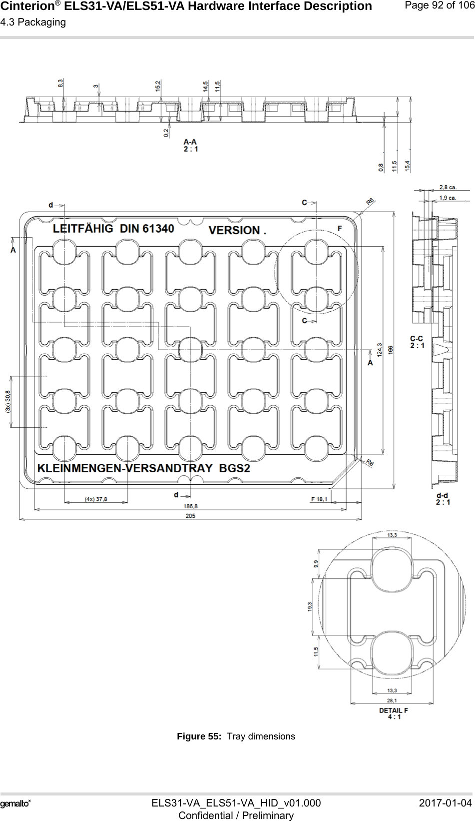
![Cinterion® ELS31-VA/ELS51-VA Hardware Interface Description4.3 Packaging92ELS31-VA_ELS51-VA_HID_v01.000 2017-01-04Confidential / PreliminaryPage 91 of 1064.3.3 TraysIf small module quantities are required, e.g., for test and evaluation purposes, ELS31-VA/ELS51-VA may be dis-tributed in trays (for dimensions see Figure 55). The small quantity trays are an alternative to the single-feed tape carriers normally used. However, the trays are not designed for machine processing. They contain modules to be (hand) soldered onto an external application (for in-formation on hand soldering see [4]).Figure 52: Small quantity trayTrays are packed and shipped in the same way as tape carriers, including a moisture barrier bag with desiccant and humidity indicator card as well as a transportation box (see also Section 4.3.2).Figure 53: Tray to ship odd module amountsFigure 54: Trays with packaging materials1:1,5](https://usermanual.wiki/Gemalto-M2M/ELS31-VA.user-manual/User-Guide-3274854-Page-91.png)
![Cinterion® ELS31-VA/ELS51-VA Hardware Interface Description6.2 Related Documents103ELS31-VA_ELS51-VA_HID_v01.000 2017-01-04Confidential / PreliminaryPage 100 of 1066.2 Related Documents[1] ELS31-VA/ELS51-VA AT Command Set[2] ELS31-VA/ELS51-VA Release Note[3] Application Note 40: Thermal Solutions[4] Application Note 48: SMT Module Integration[5] Universal Serial Bus Specification Revision 2.0, April 27, 20006.3 Terms and AbbreviationsAbbreviation DescriptionADC Analog-to-digital converterAGC Automatic Gain ControlANSI American National Standards InstituteARFCN Absolute Radio Frequency Channel NumberARP Antenna Reference PointASC0/ASC1 Asynchronous Controller. Abbreviations used for first and second serial interface of the moduleB Thermistor ConstantBER Bit Error RateBTS Base Transceiver StationCB or CBM Cell Broadcast MessageCE Conformité Européene (European Conformity)CHAP Challenge Handshake Authentication ProtocolCPU Central Processing UnitCS Coding SchemeCSD Circuit Switched DataCTS Clear to SendDAC Digital-to-Analog ConverterDAI Digital Audio InterfacedBm0 Digital level, 3.14dBm0 corresponds to full scale, see ITU G.711, A-lawDCE Data Communication Equipment (typically modems, e.g. Gemalto M2M module)DCS 1800 Digital Cellular System, also referred to as PCNDRX Discontinuous ReceptionDSB Development Support BoxDSP Digital Signal ProcessorDSR Data Set ReadyDTE Data Terminal Equipment (typically computer, terminal, printer or, for example, GSM application)](https://usermanual.wiki/Gemalto-M2M/ELS31-VA.user-manual/User-Guide-3274854-Page-100.png)