Gemalto M2M ELS31-VA CAT 1 LTE Module User Manual hid elsx1 va
Gemalto M2M GmbH CAT 1 LTE Module hid elsx1 va
Contents
- 1. user manual
- 2. User Manual
user manual
M2M.GEMALTO.COM
Cinterion® ELS31-VA/ELS51-VA
Hardware Interface Description
Version: 01.000
DocId: ELS31-VA_ELS51-VA_HID_v01.000

GENERAL NOTE
THE USE OF THE PRODUCT INCLUDING THE SOFTWARE AND DOCUMENTATION (THE "PROD-
UCT") IS SUBJECT TO THE RELEASE NOTE PROVIDED TOGETHER WITH PRODUCT. IN ANY
EVENT THE PROVISIONS OF THE RELEASE NOTE SHALL PREVAIL. THIS DOCUMENT CONTAINS
INFORMATION ON GEMALTO M2M PRODUCTS. THE SPECIFICATIONS IN THIS DOCUMENT ARE
SUBJECT TO CHANGE AT GEMALTO M2M'S DISCRETION. GEMALTO M2M GMBH GRANTS A NON-
EXCLUSIVE RIGHT TO USE THE PRODUCT. THE RECIPIENT SHALL NOT TRANSFER, COPY,
MODIFY, TRANSLATE, REVERSE ENGINEER, CREATE DERIVATIVE WORKS; DISASSEMBLE OR
DECOMPILE THE PRODUCT OR OTHERWISE USE THE PRODUCT EXCEPT AS SPECIFICALLY
AUTHORIZED. THE PRODUCT AND THIS DOCUMENT ARE PROVIDED ON AN "AS IS" BASIS ONLY
AND MAY CONTAIN DEFICIENCIES OR INADEQUACIES. TO THE MAXIMUM EXTENT PERMITTED
BY APPLICABLE LAW, GEMALTO M2M GMBH DISCLAIMS ALL WARRANTIES AND LIABILITIES.
THE RECIPIENT UNDERTAKES FOR AN UNLIMITED PERIOD OF TIME TO OBSERVE SECRECY
REGARDING ANY INFORMATION AND DATA PROVIDED TO HIM IN THE CONTEXT OF THE DELIV-
ERY OF THE PRODUCT. THIS GENERAL NOTE SHALL BE GOVERNED AND CONSTRUED
ACCORDING TO GERMAN LAW.
Copyright
Transmittal, reproduction, dissemination and/or editing of this document as well as utilization of its con-
tents and communication thereof to others without express authorization are prohibited. Offenders will be
held liable for payment of damages. All rights created by patent grant or registration of a utility model or
design patent are reserved.
Copyright © 2017, Gemalto M2M GmbH, a Gemalto Company
Trademark Notice
Gemalto, the Gemalto logo, are trademarks and service marks of Gemalto and are registered in certain
countries. Microsoft and Windows are either registered trademarks or trademarks of Microsoft Corpora-
tion in the United States and/or other countries. All other registered trademarks or trademarks mentioned
in this document are property of their respective owners.
ELS31-VA_ELS51-VA_HID_v01.000 2017-01-04
Confidential / Preliminary
Cinterion® ELS31-VA/ELS51-VA Hardware Interface Description
2
Page 2 of 106
Document Name: Cinterion® ELS31-VA/ELS51-VA Hardware Interface Description
Version: 01.000
Date: 2017-01-04
DocId: ELS31-VA_ELS51-VA_HID_v01.000
Status: Confidential / Preliminary

Cinterion® ELS31-VA/ELS51-VA Hardware Interface Description
Contents
106
ELS31-VA_ELS51-VA_HID_v01.000 2017-01-04
Confidential / Preliminary
Page 3 of 106
Contents
1 Introduction ................................................................................................................. 9
1.1 Key Features at a Glance .................................................................................. 9
1.2 ELS31-VA/ELS51-VA System Overview ......................................................... 12
1.3 Circuit Concept ................................................................................................ 13
2 Interface Characteristics .......................................................................................... 14
2.1 Application Interface ........................................................................................ 14
2.1.1 Pad Assignment.................................................................................. 14
2.1.2 Signal Properties................................................................................. 16
2.1.2.1 Absolute Maximum Ratings ................................................ 21
2.1.3 USB Interface...................................................................................... 22
2.1.3.1 Interface implementation..................................................... 23
2.1.3.2 Reducing Power Consumption............................................ 24
2.1.4 Serial Interface ASC0 ......................................................................... 25
2.1.4.1 Serial Interface Start-up Behavior ....................................... 26
2.1.5 Serial Interface ASC1 ......................................................................... 27
2.1.6 UICC/SIM/USIM Interface................................................................... 29
2.1.7 Digital Audio Interface......................................................................... 31
2.1.8 Pulse Code Modulation Interface (PCM) ............................................ 31
2.1.9 Inter IC Sound Interface (I2S).............................................................. 33
2.1.10 GPIO Interface .................................................................................... 34
2.1.11 I2C Interface ........................................................................................ 36
2.1.12 SPI Interface ....................................................................................... 38
2.1.13 Pulse Counter ..................................................................................... 39
2.1.14 HSIC Interface (ELS51-VA Only)........................................................ 39
2.1.15 SDIO Interface (ELS51-VA Only)........................................................ 39
2.1.16 Control Signals.................................................................................... 42
2.1.16.1 Status LED .......................................................................... 42
2.1.16.2 Power Indication Circuit ...................................................... 43
2.1.16.3 Host Wakeup....................................................................... 43
2.1.16.4 Fast Shutdown .................................................................... 45
2.2 RF Antenna Interface....................................................................................... 46
2.2.1 Antenna Interface Specifications ........................................................ 46
2.2.2 Antenna Installation ............................................................................ 47
2.2.3 RF Line Routing Design...................................................................... 48
2.2.3.1 RF Interface Signals Circuit Diagram Example................... 48
2.2.3.2 Line Arrangement Examples ............................................... 49
2.3 Sample Application .......................................................................................... 54
2.3.1 Prevent Back Powering....................................................................... 56
2.3.2 Sample Level Conversion Circuit........................................................ 56

Cinterion® ELS31-VA/ELS51-VA Hardware Interface Description
Contents
106
ELS31-VA_ELS51-VA_HID_v01.000 2017-01-04
Confidential / Preliminary
Page 4 of 106
3 Operating Characteristics ........................................................................................ 57
3.1 Operating Modes ............................................................................................. 57
3.2 Power Up/Power Down Scenarios................................................................... 58
3.2.1 Turn on ELS31-VA/ELS51-VA ............................................................ 58
3.2.1.1 Connecting ELS31-VA/ELS51-VA BATT Lines.................... 58
3.2.1.2 Switch on ELS31-VA/ELS51-VA Using ON Signal .............. 59
3.2.2 Restart ELS31-VA/ELS51-VA............................................................. 60
3.2.2.1 Restart ELS31-VA/ELS51-VA via AT+CFUN Command ..... 60
3.2.2.2 Restart ELS31-VA/ELS51-VA Using EMERG_RST ............ 60
3.2.3 Signal States after First Startup .......................................................... 62
3.2.4 Turn off ELS31-VA/ELS51-VA ............................................................ 63
3.2.4.1 Switch off ELS31-VA/ELS51-VA Using AT Command ......... 63
3.2.5 Automatic Shutdown ........................................................................... 64
3.2.5.1 Thermal Shutdown .............................................................. 64
3.2.5.2 Undervoltage Shutdown...................................................... 65
3.2.5.3 Overvoltage Shutdown........................................................ 65
3.3 Power Saving................................................................................................... 66
3.3.1 Power Saving while Attached to LTE Networks.................................. 66
3.3.2 Wake-up via RTS0/RTS1.................................................................... 67
3.4 Power Supply................................................................................................... 68
3.4.1 Power Supply Ratings......................................................................... 69
3.4.2 Minimizing Power Losses ................................................................... 70
3.4.3 Measuring the Supply Voltage (BATT_BB)......................................... 70
3.4.4 Monitoring Power Supply by AT Command ........................................ 70
3.5 Operating Temperatures.................................................................................. 71
3.6 Electrostatic Discharge .................................................................................... 72
3.6.1 ESD Protection for Antenna Interface................................................. 72
3.7 Blocking against RF on Interface Lines ........................................................... 73
3.8 Reliability Characteristics................................................................................. 76
4 Mechanical Dimensions, Mounting and Packaging............................................... 77
4.1 Mechanical Dimensions of ELS31-VA/ELS51-VA ........................................... 77
4.2 Mounting ELS31-VA/ELS51-VA onto the Application Platform........................ 79
4.2.1 SMT PCB Assembly ........................................................................... 79
4.2.1.1 Land Pattern and Stencil..................................................... 79
4.2.1.2 Board Level Characterization.............................................. 81
4.2.2 Moisture Sensitivity Level ................................................................... 81
4.2.3 Soldering Conditions and Temperature .............................................. 82
4.2.3.1 Reflow Profile ...................................................................... 82
4.2.3.2 Maximum Temperature and Duration.................................. 83
4.2.4 Durability and Mechanical Handling.................................................... 84
4.2.4.1 Storage Conditions.............................................................. 84
4.2.4.2 Processing Life.................................................................... 85
4.2.4.3 Baking ................................................................................. 85
4.2.4.4 Electrostatic Discharge ....................................................... 85

Cinterion® ELS31-VA/ELS51-VA Hardware Interface Description
Contents
106
ELS31-VA_ELS51-VA_HID_v01.000 2017-01-04
Confidential / Preliminary
Page 5 of 106
4.3 Packaging ........................................................................................................ 86
4.3.1 Tape and Reel .................................................................................... 86
4.3.1.1 Orientation........................................................................... 86
4.3.1.2 Barcode Label ..................................................................... 87
4.3.2 Shipping Materials .............................................................................. 88
4.3.2.1 Moisture Barrier Bag ........................................................... 88
4.3.2.2 Transportation Box .............................................................. 90
4.3.3 Trays ................................................................................................... 91
5 Regulatory and Type Approval Information ........................................................... 93
5.1 Directives and Standards................................................................................. 93
5.2 SAR requirements specific to portable mobiles ............................................... 95
5.3 Reference Equipment for Type Approval......................................................... 96
5.4 Compliance with FCC and IC Rules and Regulations ..................................... 97
6 Document Information.............................................................................................. 99
6.1 Revision History ............................................................................................... 99
6.2 Related Documents ....................................................................................... 100
6.3 Terms and Abbreviations ............................................................................... 100
6.4 Safety Precaution Notes ................................................................................ 103
7 Appendix.................................................................................................................. 104
7.1 List of Parts and Accessories......................................................................... 104

Cinterion® ELS31-VA/ELS51-VA Hardware Interface Description
Tables
106
ELS31-VA_ELS51-VA_HID_v01.000 2017-01-04
Confidential / Preliminary
Page 6 of 106
Tables
Table 1: Pad assignments............................................................................................ 15
Table 2: Signal properties ............................................................................................ 16
Table 3: Absolute maximum ratings............................................................................. 21
Table 4: Signals of the SIM interface (SMT application interface) ............................... 29
Table 5: Overview of PCM pin functions...................................................................... 32
Table 6: Overview of I2S pin functions ......................................................................... 33
Table 7: GPIO lines and possible alternative assignment............................................ 34
Table 8: SDIO interface features.................................................................................. 39
Table 9: SDIO interface lines ....................................................................................... 40
Table 10: SDIO timings.................................................................................................. 40
Table 11: Host wakeup line............................................................................................ 43
Table 12: Return loss in the active band........................................................................ 46
Table 13: RF Antenna interface LTE.............................................................................. 46
Table 14: Overview of operating modes ........................................................................ 57
Table 15: Signal states................................................................................................... 62
Table 16: Temperature dependent behavior.................................................................. 64
Table 17: Voltage supply ratings.................................................................................... 69
Table 18: Current consumption ratings.......................................................................... 69
Table 19: Board temperature ......................................................................................... 71
Table 20: Electrostatic values ........................................................................................ 72
Table 21: EMI measures on the application interface.................................................... 74
Table 22: Summary of reliability test conditions............................................................. 76
Table 23: Reflow temperature ratings............................................................................ 82
Table 24: Storage conditions ......................................................................................... 84
Table 25: Directives ....................................................................................................... 93
Table 26: Standards of North American type approval .................................................. 93
Table 27: Standards of Verizon type approval............................................................... 93
Table 28: Standards of GCF type approval.................................................................... 93
Table 29: Requirements of quality ................................................................................. 93
Table 30: Standards of the Ministry of Information Industry of the
People’s Republic of China............................................................................ 94
Table 31: Toxic or hazardous substances or elements with defined concentration
limits............................................................................................................... 94
Table 32: Antenna gain limits for FCC and IC................................................................ 97
Table 33: List of parts and accessories........................................................................ 104
Table 34: Molex sales contacts (subject to change) .................................................... 105

Cinterion® ELS31-VA/ELS51-VA Hardware Interface Description
Figures
106
ELS31-VA_ELS51-VA_HID_v01.000 2017-01-04
Confidential / Preliminary
Page 7 of 106
Figures
Figure 1: ELS31-VA/ELS51-VA system overview......................................................... 12
Figure 2: ELS31-VA/ELS51-VA baseband block diagram ............................................ 13
Figure 3: Numbering plan for connecting pads (bottom view)....................................... 14
Figure 4: USB circuit ..................................................................................................... 22
Figure 5: USB Additional ESD Protection Implementation............................................ 23
Figure 6: Serial interface ASC0..................................................................................... 25
Figure 7: ASC0 startup behavior................................................................................... 26
Figure 8: Serial interface ASC1..................................................................................... 27
Figure 9: ASC1 startup behavior................................................................................... 28
Figure 10: External UICC/SIM/USIM card holder circuit ................................................. 30
Figure 11: PCM timing short frame (4096KHz, 16kHz sample rate) ............................... 32
Figure 12: I2S timing (slave mode) .................................................................................. 33
Figure 13: GPIO startup behavior ................................................................................... 35
Figure 14: I2C interface connected to V180 .................................................................... 36
Figure 15: I2C startup behavior ....................................................................................... 37
Figure 16: Characteristics of SPI modes......................................................................... 38
Figure 17: SDIO interface timing diagrams (Input/Output).............................................. 40
Figure 18: Status signaling with LED driver .................................................................... 42
Figure 19: Power indication circuit .................................................................................. 43
Figure 20: Wake-up via RING0 ....................................................................................... 44
Figure 21: Fast shutdown timing ..................................................................................... 45
Figure 22: Antenna pads (bottom view) .......................................................................... 47
Figure 23: RF interface signals example......................................................................... 48
Figure 24: Embedded Stripline with 65µm prepreg (1080) and 710µm core .................. 49
Figure 25: Micro-Stripline on 1.0mm standard FR4 2-layer PCB - example 1 ................ 50
Figure 26: Micro-Stripline on 1.0mm Standard FR4 PCB - example 2............................ 51
Figure 27: Micro-Stripline on 1.5mm Standard FR4 PCB - example 1............................ 52
Figure 28: Micro-Stripline on 1.5mm Standard FR4 PCB - example 2............................ 53
Figure 29: Schematic diagram of ELS31-VA/ELS51-VA sample application .................. 55
Figure 30: Sample level conversion circuit...................................................................... 56
Figure 31: Sample circuit for applying power using an external µC ................................ 58
Figure 32: ON timing ....................................................................................................... 59
Figure 33: Emergency restart timing ............................................................................... 60
Figure 34: Switch off behavior......................................................................................... 63
Figure 35: Power saving and paging in LTE networks.................................................... 66
Figure 36: Wake-up via RTS0/RTS1............................................................................... 67
Figure 37: Position of reference points BATT_BB/BATT_RF and GND.......................... 70
Figure 38: ESD protection for RF antenna interface ....................................................... 72
Figure 39: EMI circuits..................................................................................................... 73
Figure 40: ELS31-VA/ELS51-VA– top and bottom view ................................................. 77
Figure 41: Dimensions of ELS31-VA/ELS51-VA (all dimensions in mm)........................ 78
Figure 42: Dimensions of ELS31-VA/ELS51-VA (all dimensions in mm) - bottom view . 78
Figure 43: Land pattern (top view) .................................................................................. 79
Figure 44: Recommended design for 120 micron thick stencil (top view, dual design)... 80
Figure 45: Reflow Profile................................................................................................. 82
Figure 46: Carrier tape .................................................................................................... 86
Figure 47: Reel direction ................................................................................................. 86
Figure 48: Barcode label on tape reel ............................................................................. 87
Figure 49: Moisture barrier bag (MBB) with imprint......................................................... 88

Cinterion® ELS31-VA/ELS51-VA Hardware Interface Description
Figures
106
ELS31-VA_ELS51-VA_HID_v01.000 2017-01-04
Confidential / Preliminary
Page 8 of 106
Figure 50: Moisture Sensitivity Label .............................................................................. 89
Figure 51: Humidity Indicator Card - HIC ........................................................................ 90
Figure 52: Small quantity tray.......................................................................................... 91
Figure 53: Tray to ship odd module amounts.................................................................. 91
Figure 54: Trays with packaging materials...................................................................... 91
Figure 55: Tray dimensions............................................................................................. 92
Figure 56: Reference equipment for Type Approval ....................................................... 96
Cinterion® ELS31-VA/ELS51-VA Hardware Interface Description
1 Introduction
13
ELS31-VA_ELS51-VA_HID_v01.000 2017-01-04
Confidential / Preliminary
Page 9 of 106
1 Introduction
This document1 describes the hardware of the Cinterion® ELS31-VA and ELS51-VA modules
for Verizon Networks. It helps you quickly retrieve interface specifications, electrical and me-
chanical details and information on the requirements to be considered for integrating further
components.
The ELS31-VA and ELS51-VA modules include a baseband, a complete dual band RF front-
end, memory and required circuitry to meet 3GPP E-UTRA (Long Term Evolution - LTE, Re-
lease 10 set of specifications) and Verizon Wireless LTE UE specifications.
The module variants differentiate a follows:
- ELS31-VA provides LTE connectivity with IP Services
- ELS51-VA adds a Linux execution environment available for customer applications
1.1 Key Features at a Glance
1. The document is effective only if listed in the appropriate Release Notes as part of the technical docu-
mentation delivered with your Gemalto M2M product.
Feature Implementation
General
Frequency bands LTE dualband: B4, B13
Output power Class 3 (+23dBm +-2dB) for LTE AWS, LTE B4
Class 3 (+23dBm +-2dB) for LTE 700, LTE FDD B13
Power supply 3.3V to 4.5V
Operating temperature
(board temperature)
Normal operation: -30°C to +80°C
Extended operation: -40°C to +90°C
Physical Dimensions: 27.60mm x 18.80mm x 2.05mm
Weight: approx. 3g
RoHS All hardware components fully compliant with EU RoHS Directive
LTE features
3GPP Release 9 DL 10Mbps, UL 5Mbps
LTE Cat. 1 data rates
SMS Point-to-point MT and MO
Text mode
Storage in mobile equipment
Software
AT commands Hayes, 3GPP TS 27.007, TS 27.005, product specific
SIM Application Toolkit SAT Release 99
Firmware update Generic update from host application over ASC0 or USB modem
OTA over ASC0 and over USB

Cinterion® ELS31-VA/ELS51-VA Hardware Interface Description
1.1 Key Features at a Glance
13
ELS31-VA_ELS51-VA_HID_v01.000 2017-01-04
Confidential / Preliminary
Page 10 of 106
Interfaces
Module interface Surface mount device with solderable connection pads (SMT application
interface). Land grid array (LGA) technology ensures high solder joint reli-
ability and allows the use of an optional module mounting socket.
For more information on how to integrate SMT modules see also [4]. This
application note comprises chapters on module mounting and application
layout issues as well as on SMT application development equipment.
USB USB 2.0 High Speed (480Mbit/s) device interface, Full Speed (12Mbit/s)
compliant
2 serial interfaces ASC0:
• 8-wire modem interface with status and control lines, unbalanced, asyn-
chronous
• Default baud rate: 115,200 baud
• Adjustable baud rates: 4,800 to 921,600, no autobauding support
• Supports RTS0/CTS0 hardware flow control.
• Indication of incoming data/SMS on RING0 (can be used to wake up
host from power down modes)
ASC1 (shared with GPIO lines):
• 4-wire, unbalanced asynchronous interface
• Default baud rate: 115,200 baud
• Adjustable baud rates: 4,800bps to 921,600bps
• Supports RTS1/CTS1 hardware flow control
UICC interface Supported SIM/USIM cards: 3V, 1.8V
Embedded UICC Module is prepared for an embedded UICC
GPIO interface 20 pads of the application interface programmable as GPIO pads (17) or
GPO pads (3):
GP(I)Os can be configured as COUNTER, FST_SHDN, ASC0, ASC1, SPI,
and DAI signal lines
Programming is done via AT commands
I2C interface Supports I2C serial interface
SPI interface Supports SPI interface
SDIO ELS51-VA only:
4 wire interface.
HSIC ELS51-VA only:
High Speed Interchip Communication interface.
ADC Analog-to-Digital Converter with one unbalanced analog input.
Digitial audio interface 4 GPIO lines can be configured as PCM/I2S lines for VoLTE communica-
tion.
Antenna interface pads 50Ω LTE main antenna, 50LTE diversity antenna
Feature Implementation

Cinterion® ELS31-VA/ELS51-VA Hardware Interface Description
1.1 Key Features at a Glance
13
ELS31-VA_ELS51-VA_HID_v01.000 2017-01-04
Confidential / Preliminary
Page 11 of 106
Power on/off, Reset
Power on/off Switch-on by hardware signal ON
Switch-off by AT command
Switch off by hardware signal GPIO4/FST_SHDN instead of AT command
Automatic switch-off in case of critical temperature and voltage conditions
Reset Orderly shutdown and reset by AT command
Emergency reset by hardware signal EMERG_RST
Evaluation kit
Evaluation module ELS31-VA/ELS51-VA module soldered onto a dedicated PCB that can be
connected to an adapter in order to be mounted onto the DSB75.
DSB75 DSB75 Development Support Board designed to test and type approve
Gemalto M2M modules and provide a sample configuration for application
engineering. A special adapter is required to connect the ELS31-VA/ELS51-
VA evaluation module to the DSB75.
Feature Implementation
Cinterion® ELS31-VA/ELS51-VA Hardware Interface Description
1.2 ELS31-VA/ELS51-VA System Overview
13
ELS31-VA_ELS51-VA_HID_v01.000 2017-01-04
Confidential / Preliminary
Page 12 of 106
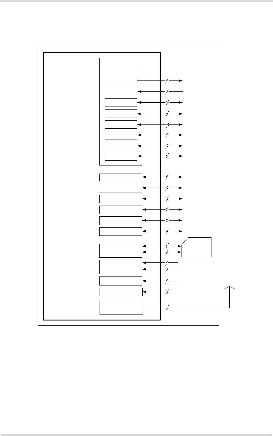
1.2 ELS31-VA/ELS51-VA System Overview
Figure 1: ELS31-VA/ELS51-VA system overview
GPIO
interface
I2C
USB
ASC0
ASC0
CONTROL
POWER
ANTENNA
(LTE dual band)
Module
SIM interface
(with SIM detection)
SIM card
Application
Power supply
Emergency reset
ON
Serial modem
interface
Serial modem
interface
I2C
USB
Antenna /
div. Antenna
GPIOs
Status LED
FST_SHDN Fast shutdown
ADC ADC
COUNTER Pulse counter
GP(I)Os
HSIC
SDIO
HSIC
SDIO
SPI SPI
SPI SPI
ASC1 Serial interface
PCM/DAI PCM/DAI
Cinterion® ELS31-VA/ELS51-VA Hardware Interface Description
1.3 Circuit Concept
13
ELS31-VA_ELS51-VA_HID_v01.000 2017-01-04
Confidential / Preliminary
Page 13 of 106
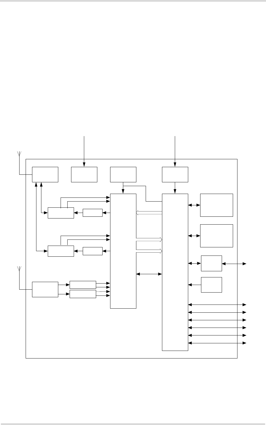
1.3 Circuit Concept
The following figure shows block diagram of the ELS31-VA/ELS51-VA module and illustrate
the major functional components (see Figure 2):
Baseband block:
• baseband processor and power management
• serial NOR flash and LPDDR RAM memory
• Application interface (SMT with connecting pads)
LTE RF section:
• RF transceiver
• RF power amplifier/front-end module and duplexers
• Receive SAW filters
Figure 2: ELS31-VA/ELS51-VA baseband block diagram
SPDT
RF Switch
B13 Duplexer
B4 Duplexer
SPDT
RF Switch
PA DC/DC PMIC
B13 SAW
B4 SAW
SQN3241
B13 PA
B4 PA
Primary
Antenna
Diversity
Antenna
TCXO
Control
RXIF1
RXIF2
TXIF
CLKREF
512Mbit LPDDR
SPI Flash
ELS31-V 256Mbit
ELS51-V 512Mbit
SIM
Level
Shifter
32.768kHz
Xtal
SQN3223
GPIO
SPI
UARTS
USB
HSIC
SDIO
SIM
Cinterion® ELS31-VA/ELS51-VA Hardware Interface Description
2 Interface Characteristics
56
ELS31-VA_ELS51-VA_HID_v01.000 2017-01-04
Confidential / Preliminary
Page 14 of 106
2 Interface Characteristics
ELS31-VA/ELS51-VA is equipped with an SMT application interface that connects to the exter-
nal application. The SMT application interface incorporates the various application interfaces
as well as the RF antenna interfaces.
2.1 Application Interface
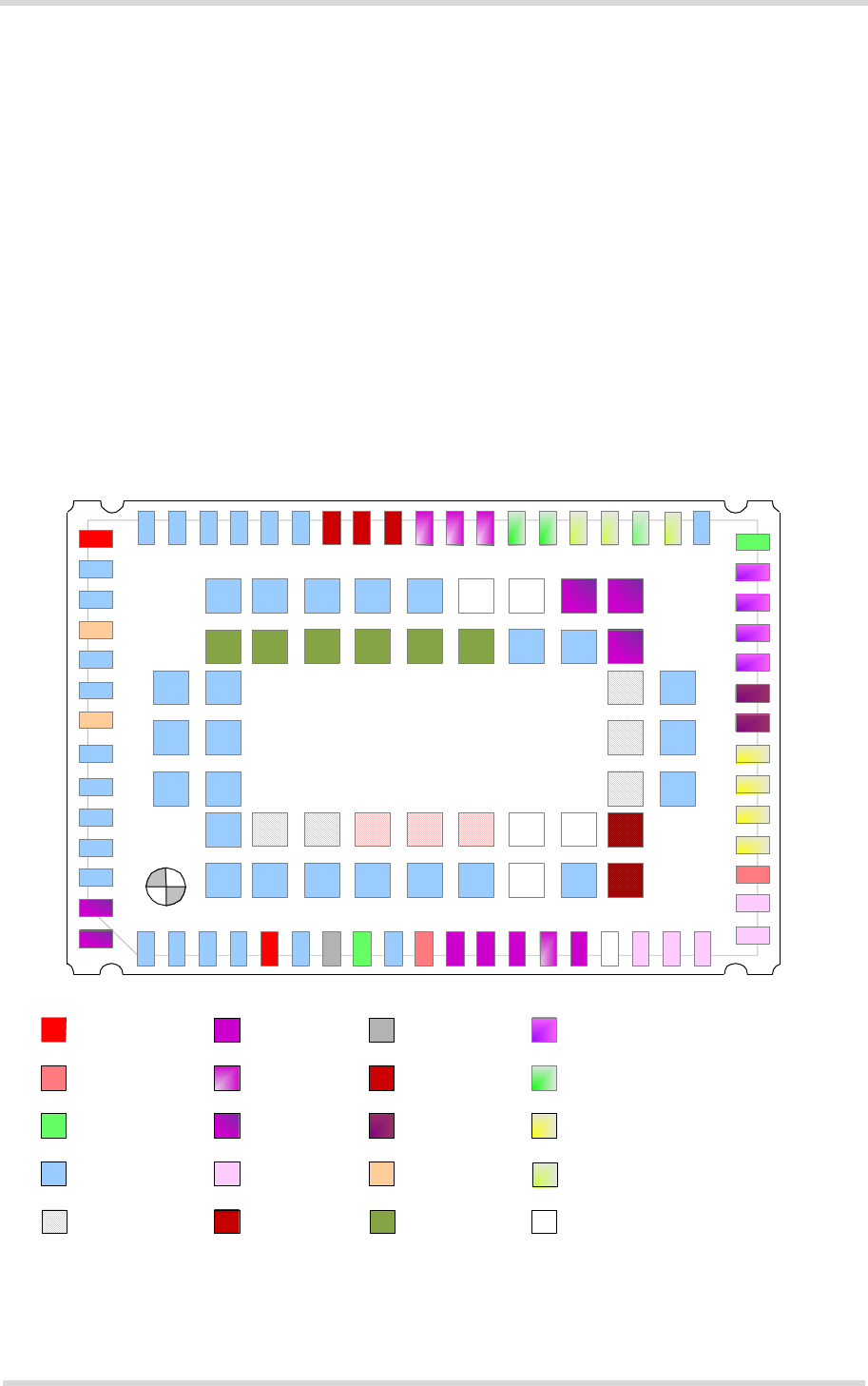
2.1.1 Pad Assignment
The SMT application interface on the ELS31-VA/ELS51-VA provides connecting pads to inte-
grate the module into external applications. Figure 3 shows the connecting pads’ numbering
plan, the following Table 1 lists the pads’ assignments.
Figure 3: Numbering plan for connecting pads (bottom view)
53
65
64
63
62
61
60
59
58
57
56
55
54
66
33
21
22
23
24
25
26
27
28
29
30
31
32
20
106
9291
9897969594
9089
85 86
93
74
99
87 88
8483
7978777675
8281
80
727170696867
105104103102101100
73
44
19181716151413121110987654321
3435363839404142434546474849505152
Supply pads : BATT+
Control pads
GND pads
ASC0 pads
SPI pads
SIM pads RF antenna pad
I2C pads
ADC pad
Supply pads : Other
Combined GPIO /DAI pads
Combined GPIO /Control pads
(LED, COUNTER, FST_SHDN)
Do not use
Not connected
Reserved
USB pads
Combined GPIO/ASC1/HSIC pads
Combined GPIO /
ASC0 pads
250
251
252
245
249
248
247
246
Test points , do not
use HSIC pads
37
SDIO pads
35
GPIO pads

Cinterion® ELS31-VA/ELS51-VA Hardware Interface Description
2.1 Application Interface
56
ELS31-VA_ELS51-VA_HID_v01.000 2017-01-04
Confidential / Preliminary
Page 15 of 106
Signal pads that are not used should not be connected to an external application.
Please note that the reference voltages listed in Table 2 are the values measured directly on
the ELS31-VA/ELS51-VA module. They do not apply to the accessories connected.
Table 1: Pad assignments
Pad no. Signal name Pad no. Signal name Pad no. Signal name
1 GND 23 GPIO20/PCM_I2S_OUT 45 USB_DP
2 GND 24 GPIO22/PCM_I2S_FSC 46 USB_DN
3 GND 25 GPIO21/PCM_I2S_IN 47 GND
4 GND 26 GPO23/PCM_I2S_CLK 48 GND
5 BATT_RF 27 I2CDAT 49 GND
6 GND 28 I2CCLK 50 GND
7 ADC1 29 GPIO17/TXD1/HOST_ACTIVE 51 GND
8 ON 30 GPIO16/RXD1/AP_WAKEUP 52 GND
9 GND 31 GPIO18/RTS1/CP_WAKEUP 53 BATT_BB
10 V180 32 GPIO19/CTS1/SUSPEND 54 GND
11 RXD0 33 EMERG_RST 55 GND
12 CTS0 34 GND 56 DIV_ANT
13 TXD0 35 GPIO25 57 GND
14 RING0/GPIO24 36 GPIO8/COUNTER 58 GND
15 RTS0 37 GPIO7 59 RF_OUT
16 Not connected 38 GPIO6 60 GND
17 CCRST 39 LED/GPO5 61 GND
18 CCIN 40 GPIO4/FST_SHDN 62 GND
19 CCIO 41 DSR0/GPIO3 63 GND
20 CCVCC 42 DCD0/GPIO2 64 GND
21 CCCLK 43 DTR0/GPIO1 65 GPIO27/SPI_CS2
22 VCORE 44 VUSB 66 GPO26/SPI_CS1
Centrally located pads
67 GND 83 Do not use (test) 99 GND
68 GND 84 GND 100 GND
69 GND 85 GND 101 GND
70 GND 86 GND 102 GND
71 GND 87 Do not use (test) 103 GND
72 Not connected 88 GND 104 Not connected
73 GND 89 GND 105 Not connected
74 Do not use (test) 90 GND 106 SPI_MOSI
75 Do not use (test) 91 Do not use (test) 245 GND
76 Do not use (test) 92 GND 246 HSIC_DATA
77 Do not use (test) 93 SDIO0 247 HSIC_STRB
78 Do not use (test) 94 SDIOCLK 248 SPI_CLK
79 Not connected 95 SDIO1 249 SPI_MISO
80 Do not use 96 SDIO2 250 GND
81 GND 97 SDIO3 251 SDIOCMD
82 GND 98 GND 252 GND

Cinterion® ELS31-VA/ELS51-VA Hardware Interface Description
2.1 Application Interface
56
ELS31-VA_ELS51-VA_HID_v01.000 2017-01-04
Confidential / Preliminary
Page 16 of 106
2.1.2 Signal Properties
Table 2: Signal properties
Function Signal name IO Signal form and level Comment
Power
supply
BATT_BB
BATT_RF
IV
Imax = 4.5V
VInorm = 3.8V
VImin = 3.3V
Imax=720mA nominal voltage 3.8V
- 300 mA for BATT_RF
- 420 mA for BATT_BB
Lines of BATT+ and GND
must be connected in
parallel for supply pur-
poses because higher
peak currents may occur.
Minimum voltage must
not fall below 3.3V includ-
ing drop, ripple, spikes
and not rise above 4.5V.
Power
supply
GND Ground Application Ground
External
supply
voltage
V180 O VOnorm = 1.80V
VOmin = 1.71 V
VOmax = 1.89V
IOmax = 50mA
CLmax = 2µF
V180 may be used to
supply level shifters at
the interfaces or to supply
external application cir-
cuits.
If unused keep line open.
VCORE O VOnorm = 1.1V
VOmin= 1.09
VOmax= 1.12
IOmax = 50mA
CLmax = 100nF
Ignition ON I BATT_BB= 4.5V
VIHmax = 5.5V
VIHmin = 2.16V
VILmax = 1.79V
VILmin=0V
BATT_BB= 3.3V
VIHmax = 5.5V
VIHmin = 1.7V
VILmax = 1.3V
VILmin = 0V
Min low time before rising edge
<=100µs
Rin = 380k
ON ___|--|____ high level min. 100µs
Edge triggered signal to
switch the module on.
Set this signal low before
and after the startup
impulse. Input is Schmitt
Trigger.
The ON signal can be
connected to BATT_BB.
In this case, the module
cannot be switched off by
a fast shutdown, but can
only be switched off by
disconnecting BATT_BB.
Emergency
restart
EMERG_RST I VIHmax = 5.5V
VIHmin = 0.85V
VILmax =0.65V
VILmin= 0V
Internal pull-up resistor
Low impulse width > 10ms
Pulse triggered signal to
reset the module. This
line must be driven low by
an open drain or open
collector driver con-
nected to GND. See also
Section 3.2.2.2.
If unused keep line open.
Cinterion® ELS31-VA/ELS51-VA Hardware Interface Description
2.1 Application Interface
56
ELS31-VA_ELS51-VA_HID_v01.000 2017-01-04
Confidential / Preliminary
Page 17 of 106
Fast
shutdown
FST_SHDN I VILmax = 0.63V
VIHmin = 1.17V
VIHmax = 1.85V
~~|___|~~ low impulse width > 10ms
This line must be driven
low.
If unused keep line open.
Note that the fast shut-
down line is originally
available as GPIO line. If
configured as fast shut-
down, the GPIO line is
assigned as follows:
GPIO4 --> FST_SHDN
USB VUSB_IN I VImin = 3V
VImax = 5.25V
Active and suspend current:
Imax < 100µA
All electrical characteris-
tics according to USB
Implementers' Forum,
USB 2.0 Specification.
If unused keep lines
open.
USB_DN I/O Full and high speed signal characteris-
tics according USB 2.0 Specification.
USB_DP
Serial
Interface
ASC0
RXD0 O VOLmax = 0.45V
VOHmin = 1.35V
VOHmax = 1.85V
VILmax = 0.63V
VILmin = -0.3V
VIHmin = 1.17V
VIHmax = 1.85V
If unused keep lines
open.
By delivery default, lines
are available as ASC0
interface lines.
If configured for use as
GPIOs the assignment is
as follows:
DTR0 --> GPIO1
DCD0 --> GPIO2
DSR0 --> GPIO3
RING0 --> GPIO24
CTS0 O
RING0 O
TXD0 I
RTS0 I
DTR0 I
DCD0 O
DSR0 O
Serial
Interface
ASC1
RXD1 O VOLmax = 0.45V
VOHmin = 1.35V
VOHmax = 1.85V
VILmax = 0.63V
VILmin = -0.3V
VIHmin = 1.17V
VIHmax = 1.85V
If unused keep lines
open.
By delivery default, ASC1
interface lines are avail-
able as GPIO lines.
If configured as ASC1
lines, the GPIO lines are
assigned as follows:
GPIO16 --> RXD1
GPIO17 --> TXD1
GPIO18 --> RTS1
GPIO19 --> CTS1
ASC1 is available as data
interface.
CTS1 O
TXD1 I
RTS1 I
Table 2: Signal properties (Continued)
Function Signal name IO Signal form and level Comment
Cinterion® ELS31-VA/ELS51-VA Hardware Interface Description
2.1 Application Interface
56
ELS31-VA_ELS51-VA_HID_v01.000 2017-01-04
Confidential / Preliminary
Page 18 of 106
I2C I2CCLK IO VOLmax = 0.45V
VOHmin = 1.35V
VOHmax = 1.85V
VILmax = 0.63V
VILmin = -0.3V
VIHmin = 1.17V
VIHmax = 1.85V
According to the I2C Bus
Specification Version 2.1
for the fast mode a rise
time of max. 300ns is per-
mitted. There is also a
maximum VOL=0.4V at
3mA specified.
Minimum R external pull-
up (connected to V180
power supply) is 391
Ohms. The value of the
pull-up depends on the
capacitive load of the
whole system (I2C Slave
+ lines).
The maximum sink cur-
rent of I2CDAT and
I2CCLK is 4.6mA.
If lines are unused keep
lines open.
I2CDAT IO
SPI SPI_CLK O VOLmax = 0.45V
VOHmin = 1.35V
VOHmax = 1.85V
VILmax = 0.63V
VILmin = -0.3V
VIHmin = 1.17V
VIHmax = 1.85V
If lines are unused keep
lines open.
By delivery default, the
SPI CS interface lines are
available as GPIO lines.
If configured as SPI lines,
the GPIO lines are
assigned as follows:
GPO26 --> SPI_CS1
GPIO27 --> SPI_CS2
SPI_MOSI O
SPI_MISO I
SPI_CS1
SPI_CS2
O
GPIO inter-
face
GPIO1-4
GPIO6-22
GPIO24,25,
27
IO VOLmax = 0.45V
VOHmin = 1.35V
VOHmax = 1.85V
VILmax = 0.63V
VILmin = -0.3V
VIHmin = 1.17V
VIHmax = 1.85V
If unused keep line open.
Please note that some
GPIO lines are or can be
can be configured by AT
command for alternative
functions:
GPIO1-GPIO3: ASC0
control lines DTR0,
DCD0, and DSR0
GPIO4: FST_SHDN
GPO5: LED
GPIO8: Pulse Counter
GPIO16-GPIO19: ASC1,
HSIC control lines
GPIO20-GPO23: PCM/
I2S lines
GPIO24: ASC0 control
line RING0
GPO26-GPIO27: SPI CS
signals
GPO5,23,26 O
Table 2: Signal properties (Continued)
Function Signal name IO Signal form and level Comment

Cinterion® ELS31-VA/ELS51-VA Hardware Interface Description
2.1 Application Interface
56
ELS31-VA_ELS51-VA_HID_v01.000 2017-01-04
Confidential / Preliminary
Page 19 of 106
Status LED LED O VOLmax = 0.45V
VOHmin = 1.35V
VOHmax = 1.85V
If unused keep line open.
By delivery default, the
line is available as LED
line.
If configured for use as
GPIO line, the LED line is
assigned as follows:
LED --> GPO5
Pulse
counter
COUNTER I VOLmax = 0.45V
VOHmin = 1.35V
VOHmax = 1.85V
VILmax = 0.63V
VILmin = -0.3V
VIHmin = 1.17V
VIHmax = 1.85V
If unused keep line open.
By delivery default, the
COUNTER line is origi-
nally available as GPIO
line. If configured for use
as COUNTER line, the
GPIO line is assigned as
follows:
GPIO8 --> COUNTER
ADC
(Analog-to-
Digital con-
verter)
ADC1 I RI = 10kOhm
VI = 0V ... 2.0V
Resolution 1024 steps
Tolerance +/-2%
ADC1 can be used as
input for external mea-
surements.
If unused keep line open.
SIM card
detection
CCIN I RI 90kOhm
VILmax = 0.63V
VIHmin = 1.17V
VIHmax = 1.85V
CCIN = High, SIM card
inserted.
For details please refer to
Section 2.1.6.
If unused keep line open.
3V SIM
Card Inter-
face
CCRST O VOHtypical = 2.065V
VOHmax = 2.95V
VOLtypical = 0.1V @1mA
VOLmax = 0.3V
Maximum cable length or
copper track to SIM card
holder should not exceed
100mm.
CCIO I/O VILmax = 0.44V
VILmin = -0.15V
VIHmin = 2.065V
VIHmax = 3.15V
VOLtypical = 0.1V @1mA
VOLmax = 0.3V
VOHmin = 2.065V at I = -10µA
VOHmax = 2.95V
CCCLK O VOHtypical = 2.065V
VOHmax = 2.95V
VOLtypical = 0.1V @1mA
VOLmax = 0.3V
CCVCC O VOmin = 2.85V
VOtyp = 2.95V
VOmax = 3.10V
IOmax = -50mA
Table 2: Signal properties (Continued)
Function Signal name IO Signal form and level Comment

Cinterion® ELS31-VA/ELS51-VA Hardware Interface Description
2.1 Application Interface
56
ELS31-VA_ELS51-VA_HID_v01.000 2017-01-04
Confidential / Preliminary
Page 20 of 106
1.8V SIM
Card Inter-
face
CCRST O VOHtypical = 1.26V
VOHmax = 1.8V
VOLtypical = 0.1V @1mA
VOLmax = 0.3V
CCIO I/O VILmax = 0.27V
VILmin=-0.15V
VIHmin = 1.26V
VIHmax = 2V
VOLtypical = 0.1V @1mA
VOLmax = 0.3V
VOHmin = 1.26V at I = -10µA
VOHmax = 1.85V
CCCLK O VOHtypical = 1.26V
VOHmax = 1.8V
VOLtypical = 0.1V @1mA
VOLmax = 0.3V
CCVCC O VOmin = 1.7V
VOtyp = 1.80V
VOmax = 1.9V
IOmax = -50mA
HSIC HSIC_DATA
HSIC_STRB
IO Signal characteristics according to
“High-Speed Inter-Chip USB Electrical
Specification”, Version 1, September
23, 2007
HSIC available with
ELS51-VA only.
See also Section 2.1.14.
SDIO SDIOCMD
SDIOCLK
SDIO0
SDIO1
SDIO2
SDIO3
IO VOLmax = 0.45V
VOHmin = 1.35V
VOHmax = 1.85V
VILmax = 0.63V
VIHmin = 1.17V
VIHmax = 1.85V
SDIO available with
ELS51-VA only.
See also Section 2.1.15.
Digital
audio
interface
(PCM/I2S)
PCM_I2S_-
CLK
IV
ILmax = 0.63V
VIHmin = 1.17V
VIHmax = 1.85V
If unused keep line open.
Note that the PCM inter-
face lines are originally
available as GPIO lines.
If configured as PCM
lines, the GPIO lines are
assigned as follows:
GPIO23 --> PCM_I2S_-
CLK
GPIO22 --> PCM_I2S_
FSC
GPIO20 --> PCM_I2S_
OUT
GPIO21 --> PCM_I2S_
IN
PCM_I2S_
FSC
I
PCM_I2S_
IN
I
PCM_I2S_
OUT
OV
OLmax = 0.45V
VOHmin = 1.35V
VOHmax = 1.85V
Table 2: Signal properties (Continued)
Function Signal name IO Signal form and level Comment

Cinterion® ELS31-VA/ELS51-VA Hardware Interface Description
2.1 Application Interface
56
ELS31-VA_ELS51-VA_HID_v01.000 2017-01-04
Confidential / Preliminary
Page 21 of 106
2.1.2.1 Absolute Maximum Ratings
The absolute maximum ratings stated in Table 3 are stress ratings under any conditions.
Stresses beyond any of these limits will cause permanent damage to ELS31-VA/ELS51-VA.
Table 3: Absolute maximum ratings
Parameter Min Max Unit
Supply voltage BATT+BB, BATT+RF -0.3 +4.5 V
Voltage at all digital lines in Power Down mode -0.3 +0.3 V
Voltage at digital lines in normal operation -0.2 2.0 V
Voltage at SIM/USIM interface, CCVCC in normal operation -0.5 +3.6 V
Voltage at ADC line in normal operation 0 2 V
Voltage at analog lines in Power Down mode -0.3 +0.3 V
V180 in normal operation +1.7 +1.9 V
Current at V180 in normal operation 50 mA
Current at VCORE in normal operation 50 mA
Cinterion® ELS31-VA/ELS51-VA Hardware Interface Description
2.1 Application Interface
56
ELS31-VA_ELS51-VA_HID_v01.000 2017-01-04
Confidential / Preliminary
Page 22 of 106
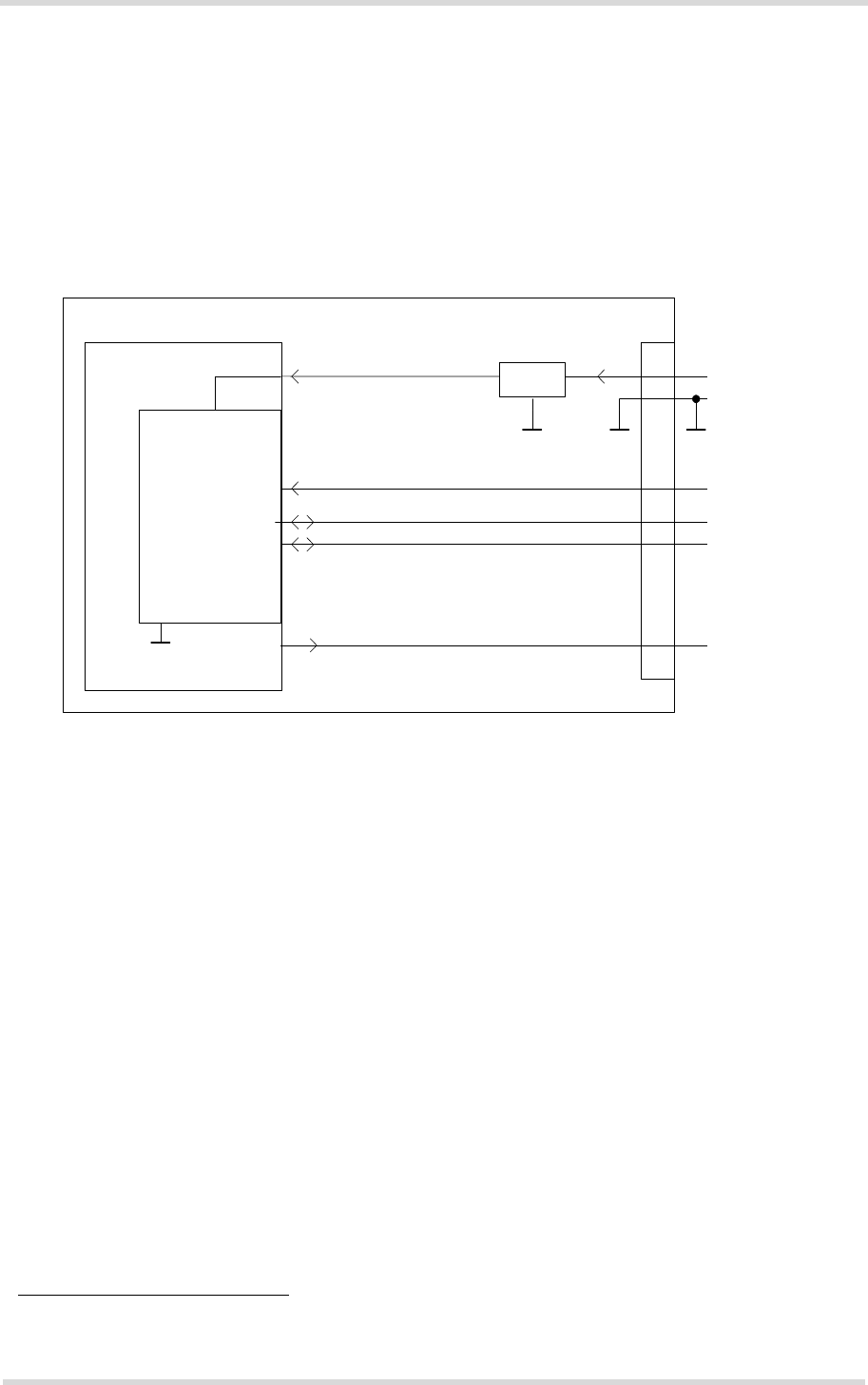
2.1.3 USB Interface
ELS31-VA/ELS51-VA supports a USB 2.0 High Speed (480Mbit/s) device interface that is Full
Speed (12Mbit/s) compliant. The USB interface is primarily intended for use as command and
data interface and for downloading firmware.
The VUSB line is used for cable detection only, this is to be supplied by the external device. The
USB circuitry in the ELS31-VA/ELS51-VA is designed to meet the USB 2.0 specification for
self-power.2.0”1.
Figure 4: USB circuit
To properly connect the module's USB interface to the external application, a USB 2.0 compat-
ible connector and cable or hardware design is required. For more information on the USB re-
lated signals see Table 2. Furthermore, the USB modem driver distributed with ELS31-VA/
ELS51-VA needs to be installed.
1. The specification is ready for download on http://www.usb.org/developers/docs/
VBUS
DP
DN
VREG (3V075)
BATT+
USB_DP2)
lin. reg.
GND
Module
Detection only VUSB_IN
USB part1)
RING0
Host wakeup
1) It is recommended to add EMI suppression filter (see section 2.1.3.1)
USB_DN2)
2) If the USB interface is operated in High Speed mode (480MHz), it is recommended to take
special care routing the data lines USB_DP and USB_DN. Application layout should in this
case implement a differential impedance of 90Ohm for proper signal integrity.
SMT
Cinterion® ELS31-VA/ELS51-VA Hardware Interface Description
2.1 Application Interface
56
ELS31-VA_ELS51-VA_HID_v01.000 2017-01-04
Confidential / Preliminary
Page 23 of 106
2.1.3.1 Interface implementation
Figure 5 shows a standard USB interfacing circuit for "off board" interfacing (connection directly
to a USB connector).
If the USB interface is directly wired to a Host interface, the additional ESD protection (U1 on
Figure 5) is not necessary, as the final product will not be a "hot swappable" item. The filter is
used to offer high impedance to higher frequency components of the USB signals. This helps
reduce any potential RF noise coming from these USB wires.
Figure 5: USB Additional ESD Protection Implementation
The digital signals USB_DP and USB_DN are sensitive to track design. Make sure these sig-
nals are routed with 90 Ohms differential resistance. If the host product is containing other USB
interfaces, then ensure that the rules used to design those are replicated here too. An overvolt-
age protection device U1 is recommended, such as ESD5V3U2U-03F.
USB_DP
USB_DN
GND
VUSB
GND
1
12
3
12
342
3
4
65
45
46
ELS31
ELS51
J1
USB-Type B
F1
U1

Cinterion® ELS31-VA/ELS51-VA Hardware Interface Description
2.1 Application Interface
56
ELS31-VA_ELS51-VA_HID_v01.000 2017-01-04
Confidential / Preliminary
Page 24 of 106
2.1.3.2 Reducing Power Consumption
While a USB connection is active, the module will never switch into SLEEP mode. Only if the
USB interface is in Suspended state or Detached (i.e., VUSB_IN = 0) is the module able to
switch into SLEEP mode thereby saving power. There are two possibilities to enable power re-
duction mechanisms:
• Recommended implementation of USB Suspend/Resume/Remote Wakeup:
The USB host should be able to bring its USB interface into the Suspended state as
described in the “Universal Serial Bus Specification Revision 2.0“1. For this functionality to
work, the VUSB_IN line should always be kept enabled. On incoming calls and other events
ELS31-VA/ELS51-VA will then generate a Remote Wakeup request to resume the USB
host controller.
See also [5] (USB Specification Revision 2.0, Section 10.2.7, p.282):
"If USB System wishes to place the bus in the Suspended state, it commands the Host Con-
troller to stop all bus traffic, including SOFs. This causes all USB devices to enter the Sus-
pended state. In this state, the USB System may enable the Host Controller to respond to
bus wakeup events. This allows the Host Controller to respond to bus wakeup signaling to
restart the host system."
• Implementation for legacy USB applications not supporting USB Suspend/Resume:
As an alternative to the regular USB suspend and resume mechanism it is possible to
employ the RING0 line to wake up the host application in case of incoming calls or events
signalized by URCs while the USB interface is in Detached state (i.e., VUSB_IN = 0). Every
wakeup event will force a new USB enumeration. Therefore, the external application has to
carefully consider the enumeration timings to avoid loosing any signalled events. For details
on this host wakeup functionality see Section 2.1.16.3.
Note: Existing data connections will not be disconnected even if the USB interface is in de-
tached state. URCs will be queued during detached state, but may be signaled to the host via
host wakeup line RING0.
1. The specification is ready for download on http://www.usb.org/developers/docs/
Cinterion® ELS31-VA/ELS51-VA Hardware Interface Description
2.1 Application Interface
56
ELS31-VA_ELS51-VA_HID_v01.000 2017-01-04
Confidential / Preliminary
Page 25 of 106
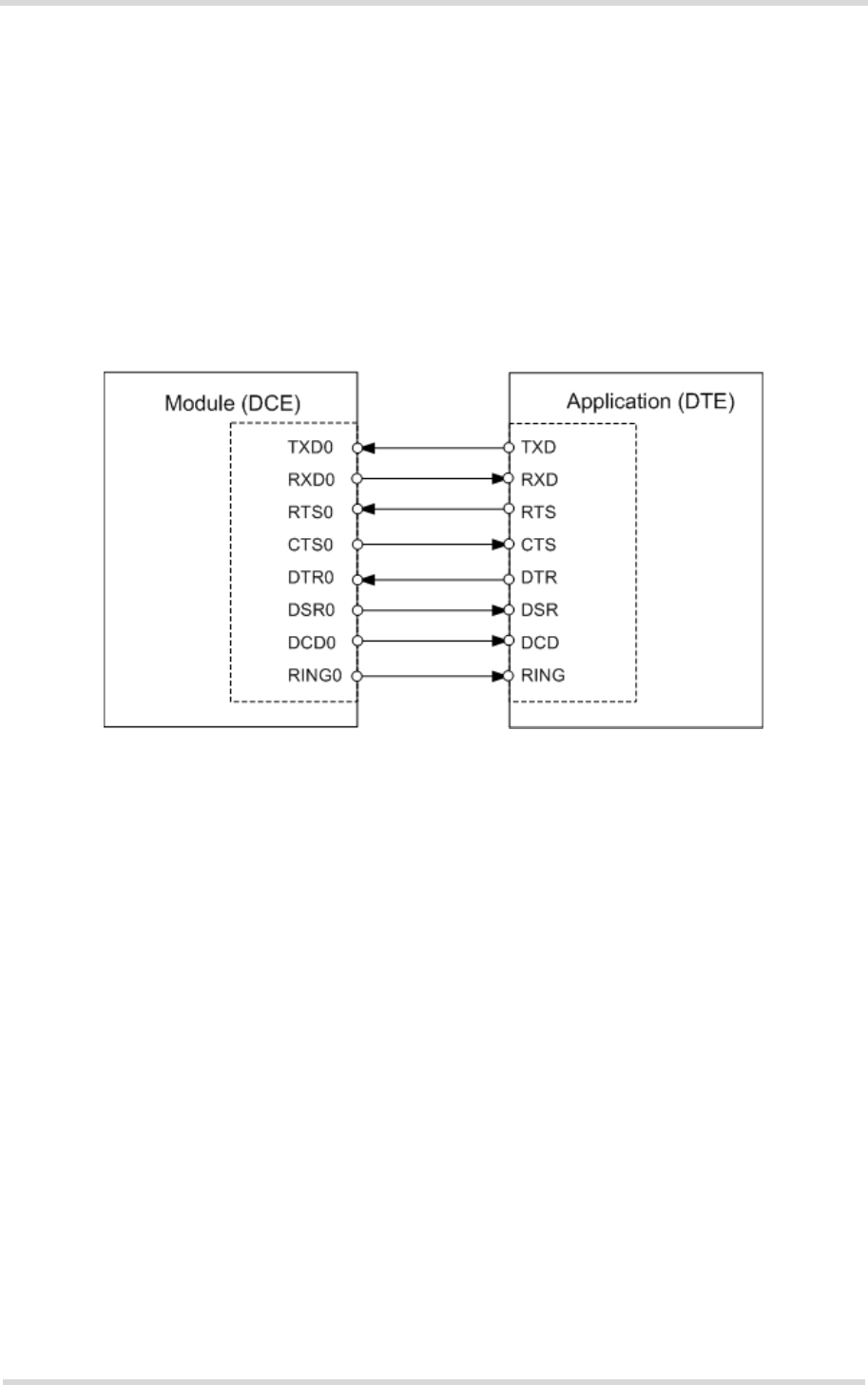
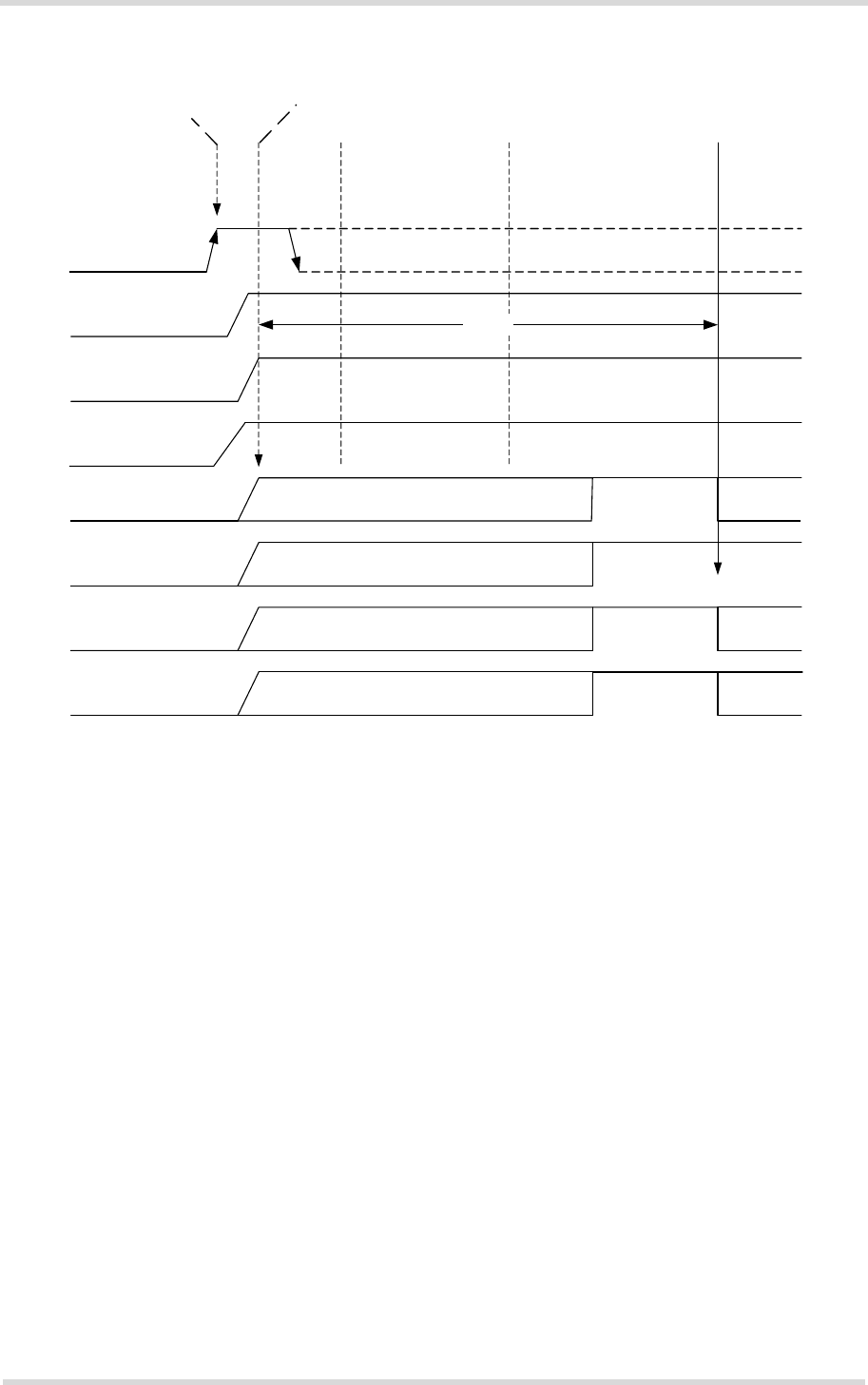
2.1.4 Serial Interface ASC0
ELS31-VA/ELS51-VA offers an 8-wire unbalanced, asynchronous modem interface ASC0 con-
forming to ITU-T V.24 protocol DCE signalling. The electrical characteristics do not comply with
ITU-T V.28. The significant levels are 0V (for low data bit or active state) and 1.8V (for high data
bit or inactive state). For electrical characteristics please refer to Table 2. For an illustration of
the interface line’s startup behavior see Figure 7.
ELS31-VA/ELS51-VA is designed for use as a DCE. Based on the conventions for DCE-DTE
connections it communicates with the customer application (DTE) using the following signals:
• Port TXD @ application sends data to the module’s TXD0 signal line
• Port RXD @ application receives data from the module’s RXD0 signal line
Figure 6: Serial interface ASC0
Features:
• Includes the data lines TXD0 and RXD0, the status lines RTS0 and CTS0 and, in addition,
the modem control lines DTR0, DSR0, DCD0 and RING0.
• Configured for 8 data bits, no parity and 1 stop bit.
• ASC0 can be operated at fixed bit rates from 4800bps up to 921600bps.
• Supports RTS0/CTS0 hardware flow control. Communication is possible by using only RXD
and TXD lines, if RTS0 is pulled low.
• Wake up from SLEEP mode by RTS0 activation (high to low transition; see Section 3.3.2).
The ASC0 interface is dedicated to signaling via AT commands (3GPP standard 27.007 + mod-
ule specific AT commands).
Note: The ASC0 modem control lines DTR0, DCD0, DSR0 and RING0 can also be configured
as GPIO lines. If configured as GPIO lines, these GPIO lines are assigned as follows:
DTR0 --> GPIO1, DCD0 --> GPIO2, DSR0 --> GPIO3 and RING0 --> GPIO24.
Cinterion® ELS31-VA/ELS51-VA Hardware Interface Description
2.1 Application Interface
56
ELS31-VA_ELS51-VA_HID_v01.000 2017-01-04
Confidential / Preliminary
Page 26 of 106
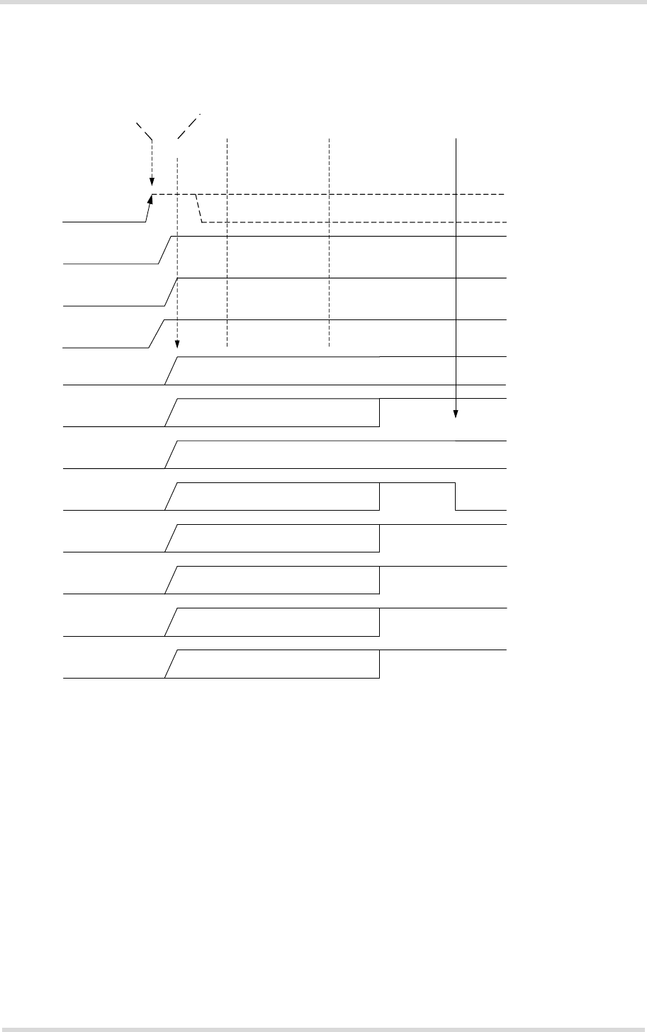
2.1.4.1 Serial Interface Start-up Behavior
The following figure shows the startup behavior of the asynchronous serial interface ASC0.
For pull-up and pull-down values see Table 15.
Figure 7: ASC0 startup behavior
No data must be sent over the ASC0 interface before the interface is active and ready to re-
ceive data (see Section 3.2.1).
TXD0
RXD0
RTS0
CTS0
DTR0
DSR0
DCD0
RING0
ON
EMERG_RST
Power supply active
Start up
Firmware
initialization
Command interface
initialization
Interface
active
V180
VCORE
Reset
state
Cinterion® ELS31-VA/ELS51-VA Hardware Interface Description
2.1 Application Interface
56
ELS31-VA_ELS51-VA_HID_v01.000 2017-01-04
Confidential / Preliminary
Page 27 of 106
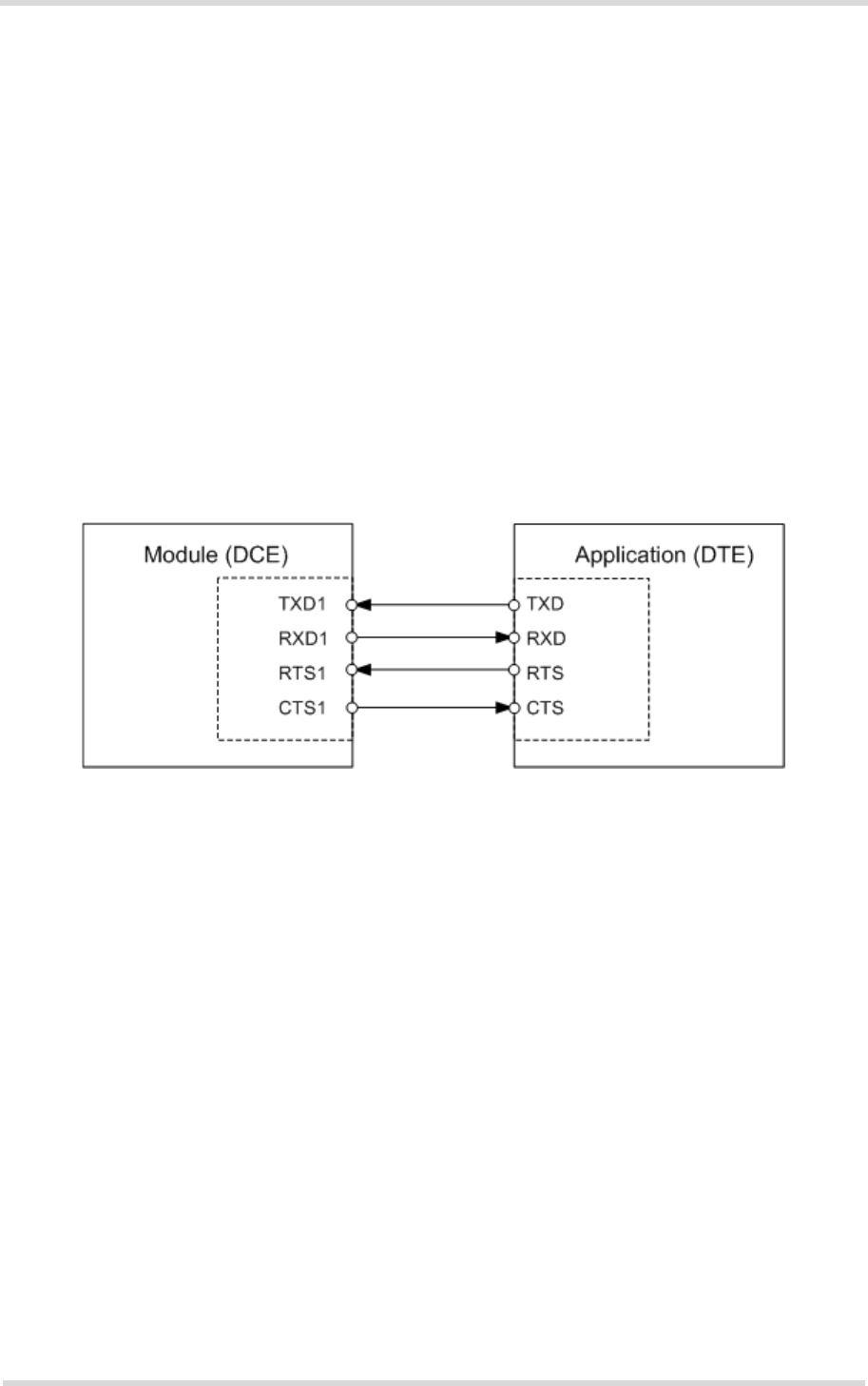
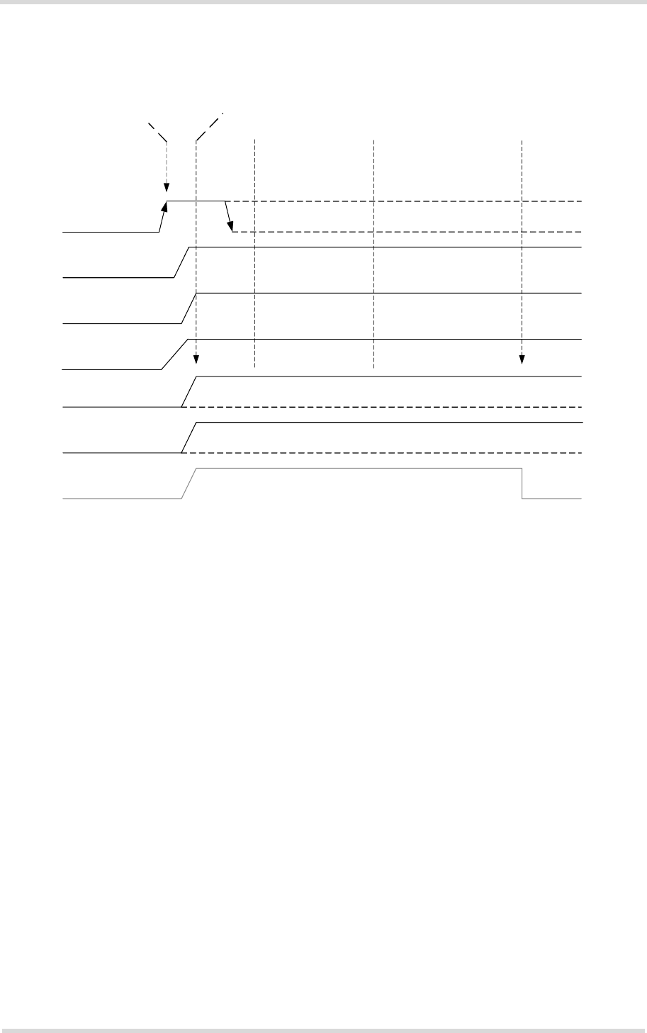
2.1.5 Serial Interface ASC1
ELS31-VA/ELS51-VA provides a 4-wire unbalanced, asynchronous modem interface ASC1
conforming to ITU-T V.24 protocol DCE signaling. The electrical characteristics do not comply
with ITU-T V.28. The significant levels are 0V (for low data bit or active state) and 1.8V (for high
data bit or inactive state). For electrical characteristics please refer to Table 2. For an illustra-
tion of the interface line’s startup behavior see Figure 9. ASC1 can only be used as data inter-
face.
The ASC1 interface lines are originally available as GPIO lines. If configured as ASC1 lines,
the GPIO lines are assigned as follows: GPIO16 --> RXD1, GPIO17 --> TXD1, GPIO18 -->
RTS1 and GPIO19 --> CTS1. Configuration is done by AT command (see [1]: AT^SCFG). The
configuration is non-volatile and becomes active after a module restart.
ELS51-VA is designed for use as a DCE. Based on the conventions for DCE-DTE connections
it communicates with the customer application (DTE) using the following signals:
• Port TXD @ application sends data to module’s TXD1 signal line
• Port RXD @ application receives data from the module’s RXD1 signal line
Figure 8: Serial interface ASC1
Features
• Includes only the data lines TXD1 and RXD1 plus RTS1 and CTS1 for hardware hand-
shake.
• On ASC1 no RING line is available.
• Configured for 8 data bits, no parity and 1 or 2 stop bits.
• ASC1 can be operated at fixed bit rates from 4800 bps to 921600 bps.
• Supports RTS1/CTS1 hardware flow control. Communication is possible by using only RXD
and TXD lines, if RTS1 is pulled low.
• Wake up from SLEEP mode by RTS0 activation (high to low transition; see Section 3.3.2).
AT commands for signaling are not supported on ASC1 interface. ASC1 is intended only for
data transfer in a Linux environment.
The following figure shows the startup behavior of the asynchronous serial interface ASC1.
Cinterion® ELS31-VA/ELS51-VA Hardware Interface Description
2.1 Application Interface
56
ELS31-VA_ELS51-VA_HID_v01.000 2017-01-04
Confidential / Preliminary
Page 28 of 106
*) For pull-down values see Table 15.
Figure 9: ASC1 startup behavior
TXD1
RXD1
RTS1
CTS1
ON
Power supply active
Start up
Firmware
initialization
Command interface
initialization
Interface
active
V180
VCORE
EMERG_RST
Reset
state
~ 15sec
Cinterion® ELS31-VA/ELS51-VA Hardware Interface Description
2.1 Application Interface
56
ELS31-VA_ELS51-VA_HID_v01.000 2017-01-04
Confidential / Preliminary
Page 29 of 106
2.1.6 UICC/SIM/USIM Interface
ELS31-VA/ELS51-VA has an integrated UICC/SIM/USIM interface compatible with the 3GPP
31.102 and ETSI 102 221. This is wired to the host interface in order to be connected to an
external SIM card holder. Five pads on the SMT application interface are reserved for the SIM
interface.
The UICC/SIM/USIM interface supports 3V and 1.8V SIM cards. Please refer to Table 2 for
electrical specifications of the UICC/SIM/USIM interface lines depending on whether a 3V or
1.8V SIM card is used.
The CCIN signal serves to detect whether a tray (with SIM card) is present in the card holder.
The CCIN signal must be connected to V180 for the detection to work on the module. Other-
wise the SIM card can never be detected by the module.
Using the CCIN signal is mandatory for compliance with the GSM 11.11 recommendation if the
mechanical design of the host application allows the user to remove the SIM card during oper-
ation. To take advantage of this feature, an appropriate SIM card detect switch is required on
the card holder. For example, this is true for the model supplied by Molex, which has been test-
ed to operate with ELS31-VA/ELS51-VA and is part of the Gemalto M2M reference equipment
submitted for type approval. See Section 7.1 for Molex ordering numbers.
Note: No guarantee can be given, nor any liability accepted, if loss of data is encountered after
removing the SIM card during operation. Also, no guarantee can be given for properly initializ-
ing any SIM card that the user inserts after having removed the SIM card during operation. In
this case, the application must restart ELS31-VA/ELS51-VA.
Table 4: Signals of the SIM interface (SMT application interface)
Signal Description
GND Separate ground connection for SIM card to improve EMC.
CCCLK Chipcard clock
CCVCC SIM supply voltage.
CCIO Serial data line, input and output.
CCRST Chipcard reset
CCIN Input on the baseband processor for detecting a SIM card tray in the holder. If the SIM is
removed during operation the SIM interface is shut down immediately to prevent destruc-
tion of the SIM. The CCIN signal is by default low and will change to high level if a SIM card
is inserted.
The CCIN signal is mandatory for applications that allow the user to remove the SIM card
during operation.
The CCIN signal is solely intended for use with a SIM card. It must not be used for any other
purposes. Failure to comply with this requirement may invalidate the type approval of
ELS31-VA/ELS51-VA.
Cinterion® ELS31-VA/ELS51-VA Hardware Interface Description
2.1 Application Interface
56
ELS31-VA_ELS51-VA_HID_v01.000 2017-01-04
Confidential / Preliminary
Page 30 of 106
The figure below shows a circuit to connect an external SIM card holder.
Figure 10: External UICC/SIM/USIM card holder circuit
The total cable length between the SMT application interface pads on ELS31-VA/ELS51-VA
and the pads of the external SIM card holder must not exceed 100mm in order to meet the
specifications of 3GPP TS 51.010-1 and to satisfy the requirements of EMC compliance.
To avoid possible cross-talk from the CCCLK signal to the CCIO signal be careful that both
lines are not placed closely next to each other. A useful approach is using a GND line to shield
the CCIO line from the CCCLK line.
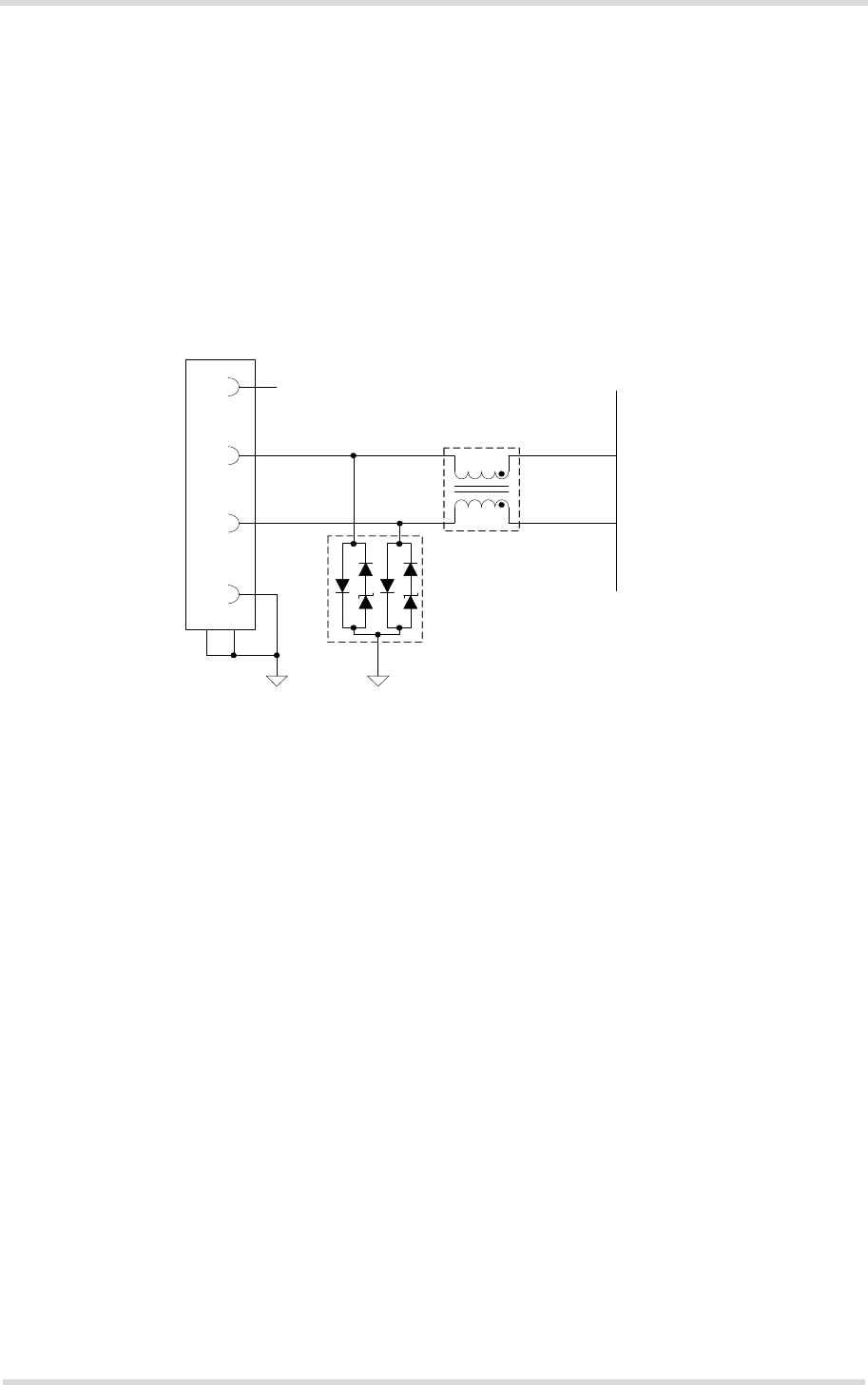
The ELS31-VA/ELS51-VA includes embedded ESD protection for the SIM interface that com-
plies to ETSI EN 301 489-1/7: Contact discharge: ± 4kV, air discharge: ± 8kV.
SIM
CCVCC
CCRST
CCIO
CCCLK
220nF
1nF
CCIN
V180

Cinterion® ELS31-VA/ELS51-VA Hardware Interface Description
2.1 Application Interface
56
ELS31-VA_ELS51-VA_HID_v01.000 2017-01-04
Confidential / Preliminary
Page 31 of 106
2.1.7 Digital Audio Interface
ELS31-VA/ELS51-VA supports a digital audio interface that can be employed either as pulse
code modulation interface (see Section 2.1.8) or as inter IC sound interface (see Section 2.1.9).
Operation of these interface variants is mutually exclusive, and can be configured by AT com-
mand (see [1])). Default setting is pulse code modulation.
2.1.8 Pulse Code Modulation Interface (PCM)
Note: ELS31-VA/ELS51-VA's PCM interface is reserved for future use. Usage as digital audio
interface is currently not supported.
ELS31-VA/ELS51-VA's PCM interface can be used to connect audio devices capable of pulse
code modulation. The PCM functionality is limited to the use of covers the use of narrowband
codecs with 8kHz sample rate and wideband codecs with 16kHz sample rate onlyas well. Con-
figured for wideband the The PCM interface runs at 16 kHz sample rate (62.5µs frame length),
while the signal processing maintains this rate in a wideband AMR call or samples automati-
cally down to 8kHz in a narrowband call. Therefore, the PCM sample rate is independent of the
audio bandwidth of the call.
The PCM interface has the following implementation:
•Slave mode
• Short frame synchronization, long frame synchronization
• 8kHz and 16kHz sample rate
• 256kHz, 512kHz, 2048kHz bit clock at 8kHz sample rate
• 256kHz, 512kHz, 1024kHz, 4096kHz bit clock at 16kHz sample rate
For the PCM configuration the AT^SAIC command parameters <clock>, <mode>, <frame_-
mode>, <ext_clk_mode> and <sample_rate> (see [1]) cannot be configured in any combina-
tion. The following notes, must be considered while configuring the PCM interface:
ELS31-VA/ELS51-VA’s digital audio interface can only be operated in slave mode. Therefore,
the <mode> parameter must be set to <1>, and the <ext_clk_mode> be set to not permanent
resp. off. Further, while in slave mode the <clock>, <frame_mode> and <sample_rate> must
be set according to the characteristics of the external master. There is no automatic detection
of the received clock frequency, frame length and sample rate.
Four GPIOs can be configured by AT command as PCM signals: GPIO20 --> PCM_I2S_OUT,
GPIO21--> PCM_I2S_IN, GPIO22 --> PCM_I2S_FSC and GPIO23 --> PCM_I2S_CLK. The
setting is non-volatile and becomes active after a module restart (see also [1]).
Table 5 describes the available DAI/PCM lines at the digital audio interface. For electrical de-
tails see Section 2.1.2.
Cinterion® ELS31-VA/ELS51-VA Hardware Interface Description
2.1 Application Interface
56
ELS31-VA_ELS51-VA_HID_v01.000 2017-01-04
Confidential / Preliminary
Page 32 of 106
Note: PCM data is always formatted as 16-bit uncompressed two’s complement. Also, all PCM
data and frame synchronization signals are written to the PCM bus on the rising clock edge and
read on the falling edge.
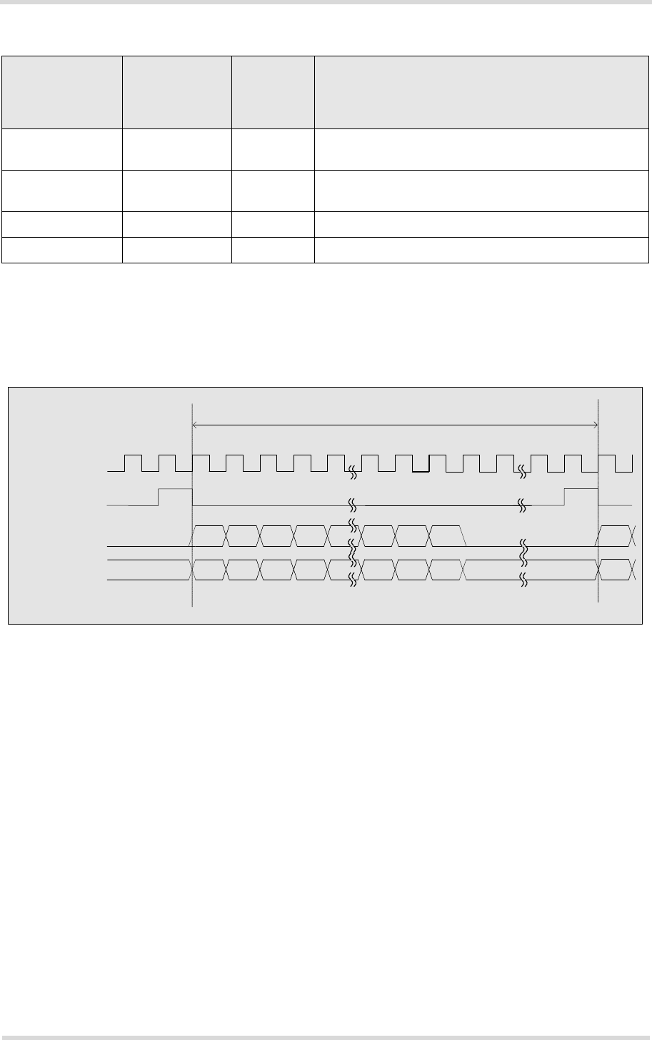
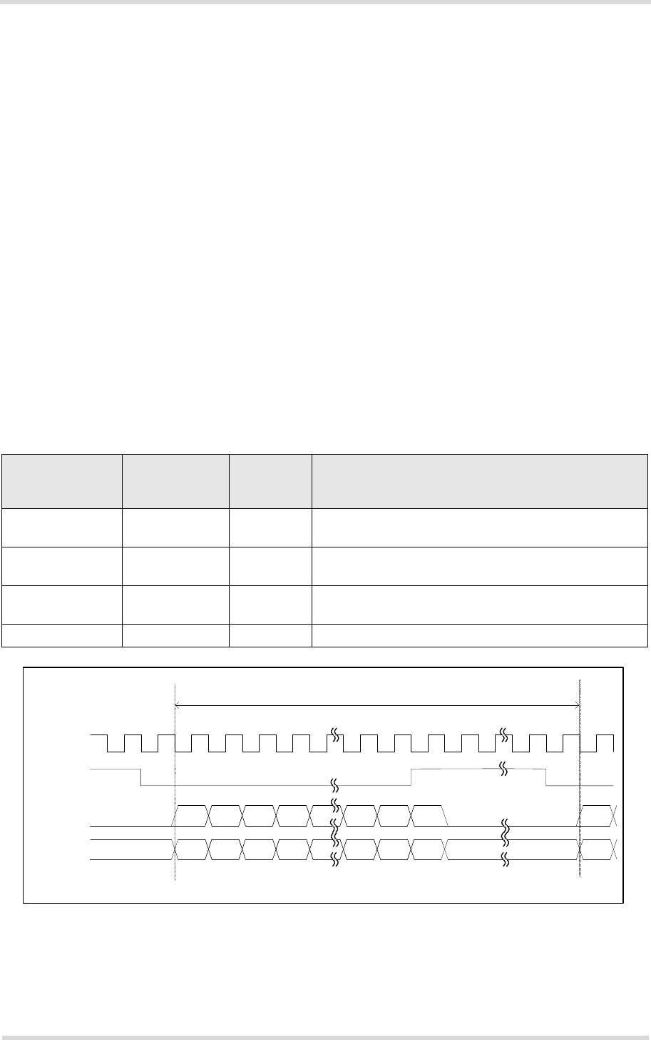
The timing of a PCM short frame is shown in Figure 11.
Figure 11: PCM timing short frame (4096KHz, 16kHz sample rate)
Configured to short frame synchronization, the pulse on PCM_I2S_FSC should be one clock
period wide and occur one clock before the data, using long frame the pulse should have a duty
cycle of 50% starting with the first data bit.
Characteristics of Audio Modes
ELS31-VA/ELS51-VA has various audio modes selectable with AT^SNFS (for details on
AT^SNFS see [1]).
Audio mode 1 with its default settings is used for type approval with the Votronic handset via
the DSB75 codec adapter. The handset is adjusted for the type 3.2 low-leakage ear simulator
for narrowband and wideband calls.
The other modes are customer specific modes, and can as such be prepared for specific re-
quirements.
Table 5: Overview of PCM pin functions
Signal name on
B2B connector
SMT application
interface
Signal
configuration
inactive
Signal
direction:
Slave
Description
PCM_I2S_OUT PD O PCM data from ELS31-VA/ELS51-VA to external
codec
PCM_I2S_IN PD I PCM data from external codec to ELS31-VA/
ELS51-VA
PCM_I2S_FSC PD I Frame synchronization signal from external codec
PCM_I2S_CLK PD I Bit clock from external codec
MSB
MSB
LSB
LSB
14 13
14 13
1
1
12
12
2
2
MSB
MSB
62.5 µs
PCM_I2S_CLK
PCM_I2S_FSC
PCM_I2S_OUT
PCM_I2S_IN
Cinterion® ELS31-VA/ELS51-VA Hardware Interface Description
2.1 Application Interface
56
ELS31-VA_ELS51-VA_HID_v01.000 2017-01-04
Confidential / Preliminary
Page 33 of 106
2.1.9 Inter IC Sound Interface (I2S)
The I2S Interface is a standardized bidirectional I2S ("Inter-IC Sound Interface") based digital
audio interface for transmission of mono voice signals for telephony services.
The I2S interface can be enabled and configured using the AT command AT^SAIC (see [1]).
An activation is possible only out of call and out of tone presentation. The I2S properties and
capabilities comply with the requirements laid out in the Phillips I2S Bus Specifications, revised
June 5, 1996.
The I2S interface has the following characteristics:
• Bit clock mode: Slave, requires external master clock input
• Sampling rate: 8KHz (narrowband), 16KHz (wideband)
• 256kHz bit clock at 8kHz sample rate
• 512kHz bit clock at 16kHz sample rate
• Frame length: 32 bit stereo voice signal (16 bit word length)
The digital audio interface lines available for the PCM interface are also available for the I2S
interface. In I2S mode they have the same electrical characteristics.
Table 6 lists the available I2S interface signals, Figure 12 shows the I2S timing.
Figure 12: I2S timing (slave mode)
Table 6: Overview of I2S pin functions
Signal name on
SMT application
interface
Signal
configuration
inactive
Signal
direction:
Slave
Description
PCM_I2S_OUT PD O I2S data from ELS31-VA/ELS51-VA to external
codec
PCM_I2S_IN PD I I2S data from external codec to ELS31-VA/ELS51-
VA
PCM_I2S_FSC PD I Frame synchronization signal from external codec
Word alignment (WS)
PCM_I2S_CLK PD I Bit clock from external codec
PCM_I2S_CLK
PCM_I2S_OUT
PCM_I2S_IN
PCM_I2S_FSC
MSB
MSB
LSB
LSB
14 13
14 13
1
1
12
12
2
2
MSB
MSB
125 µs
Cinterion® ELS31-VA/ELS51-VA Hardware Interface Description
2.1 Application Interface
56
ELS31-VA_ELS51-VA_HID_v01.000 2017-01-04
Confidential / Preliminary
Page 34 of 106
2.1.10 GPIO Interface
ELS31-VA/ELS51-VA offers a GPIO interface with 17 GPIO and 3 GPO lines. The lines are
shared with other interfaces or functions: Fast shutdown (see Section 2.1.16.4), status LED
(see Section 2.1.16.1), a pulse counter (see Section 2.1.13), ASC0 (see Section 2.1.4), ASC1
(see Section 2.1.5), SPI (see Section 2.1.12), HSIC (see Section 2.1.14), and digital audio in-
terface (DAI; see Section 2.1.7).
The following table shows the configuration variants for the GPIO pads. All variants are mutu-
ally exclusive, i.e. a pad configured for instance as Status LED is locked for alternative usage.
After startup, the above mentioned alternative GPIO line assignments can be configured using
AT commands (see [1]). The configuration is non-volatile and available after module restart.
Notes:
• GPO5, GPO23 and GPO26 are GPOs only.
Table 7: GPIO lines and possible alternative assignment
GPIO Fast
Shutdown Status
LED Pulse
Counter ASC0 ASC1 SPI HSIC PCM
GPIO1 DTR0
GPIO2 DCD0
GPIO3 DSR0
GPIO4 FST_SHDN
GPO5 LED
GPIO6
GPIO7
GPIO8 COUNTER
GPIO16 RXD1 AP_WAKEUP
GPIO17 TXD1 HOST_ACTIVE
GPIO18 RTS1 CP_WAKEUP
GPIO19 CTS1 SUSPEND
GPIO20 PCM_I2S_OUT
GPIO21 PCM_I2S_IN
GPIO22 PCM_I2S_FSC
GPO23 PCM_I2S_CLK
GPIO24 RING0
GPIO25
GPO26 SPI_CS1
GPIO27 SPI_CS2
Cinterion® ELS31-VA/ELS51-VA Hardware Interface Description
2.1 Application Interface
56
ELS31-VA_ELS51-VA_HID_v01.000 2017-01-04
Confidential / Preliminary
Page 35 of 106
The following figure shows the startup behavior of the GPIO interface. With an active state of
the ASC0 interface line CTS0, the initialization of the GPIO interface lines is also finished.
*) For pull down values see Table 15.
Figure 13: GPIO startup behavior
GPIO1 - 8 Hi-Z
CTS0
ON
EMERG_RST
Power supply active
Start up
Firmware
initialization
Command interface
initialization
Interface
active
V180
VCORE
GPIO16 - 27 Hi-Z
Reset
state
Cinterion® ELS31-VA/ELS51-VA Hardware Interface Description
2.1 Application Interface
56
ELS31-VA_ELS51-VA_HID_v01.000 2017-01-04
Confidential / Preliminary
Page 36 of 106
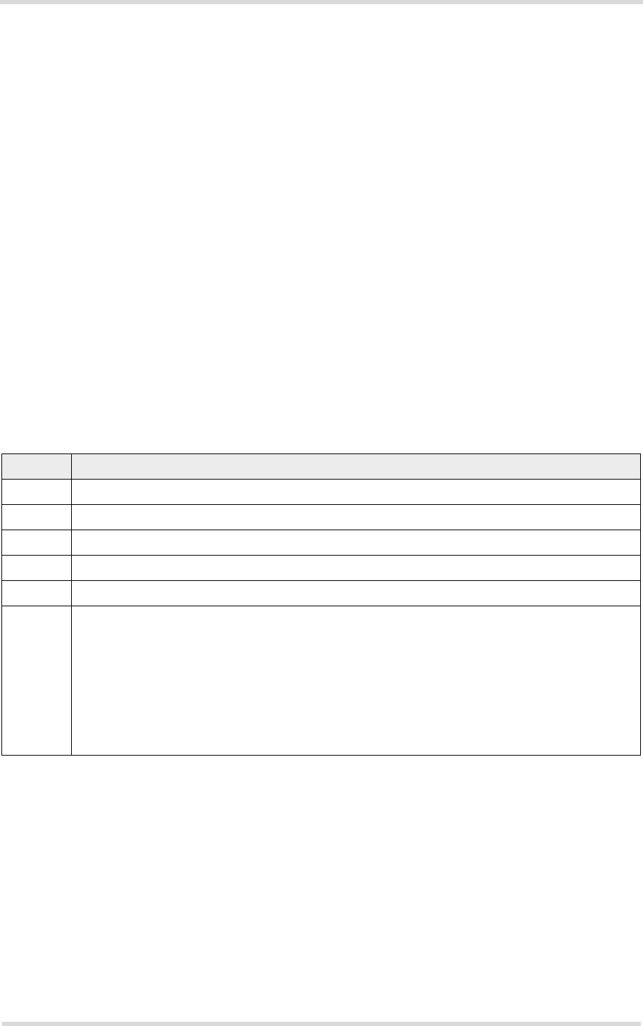
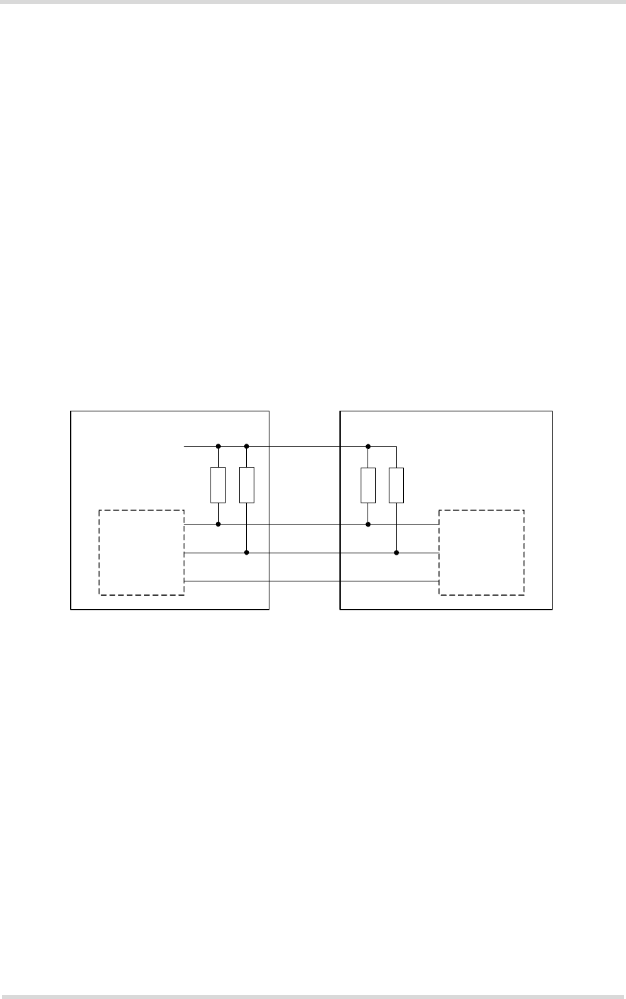
2.1.11 I2C Interface
I2C is a serial, 8-bit oriented data transfer bus for bit rates up to 100kbps. It consists of two lines,
the serial data line I2CDAT and the serial clock line I2CCLK. The module acts as a single mas-
ter device, e.g. the clock I2CCLK is driven by the module. I2CDAT is a bi-directional line. Each
device connected to the bus is software addressable by a unique 7-bit address, and simple
master/slave relationships exist at all times. The module operates as master-transmitter or as
master-receiver. The customer application transmits or receives data only on request of the
module.
To configure and activate the I2C bus use the AT^SSPI command. Detailed information on the
AT^SSPI command as well explanations on the protocol and syntax required for data transmis-
sion can be found in [1].
The I2C interface can be powered via the V180 line of ELS31-VA/ELS51-VA. If connected to
the V180 line, the I2C interface will properly shut down when the module enters the Power
Down mode.
In the application I2CDAT and I2CCLK lines need to be connected to a positive supply voltage
via a pull-up resistor. For electrical characteristics please refer to Table 2.
Figure 14: I2C interface connected to V180
Note: Good care should be taken when creating the PCB layout of the host application: The
traces of I2CCLK and I2CDAT should be equal in length and as short as possible.
I2CCLK
I2CDAT
GND
I2CCLK
I2CDAT
GND
Module Application
V180
R pull up
R pull up
R pull up
R pull up
Cinterion® ELS31-VA/ELS51-VA Hardware Interface Description
2.1 Application Interface
56
ELS31-VA_ELS51-VA_HID_v01.000 2017-01-04
Confidential / Preliminary
Page 37 of 106
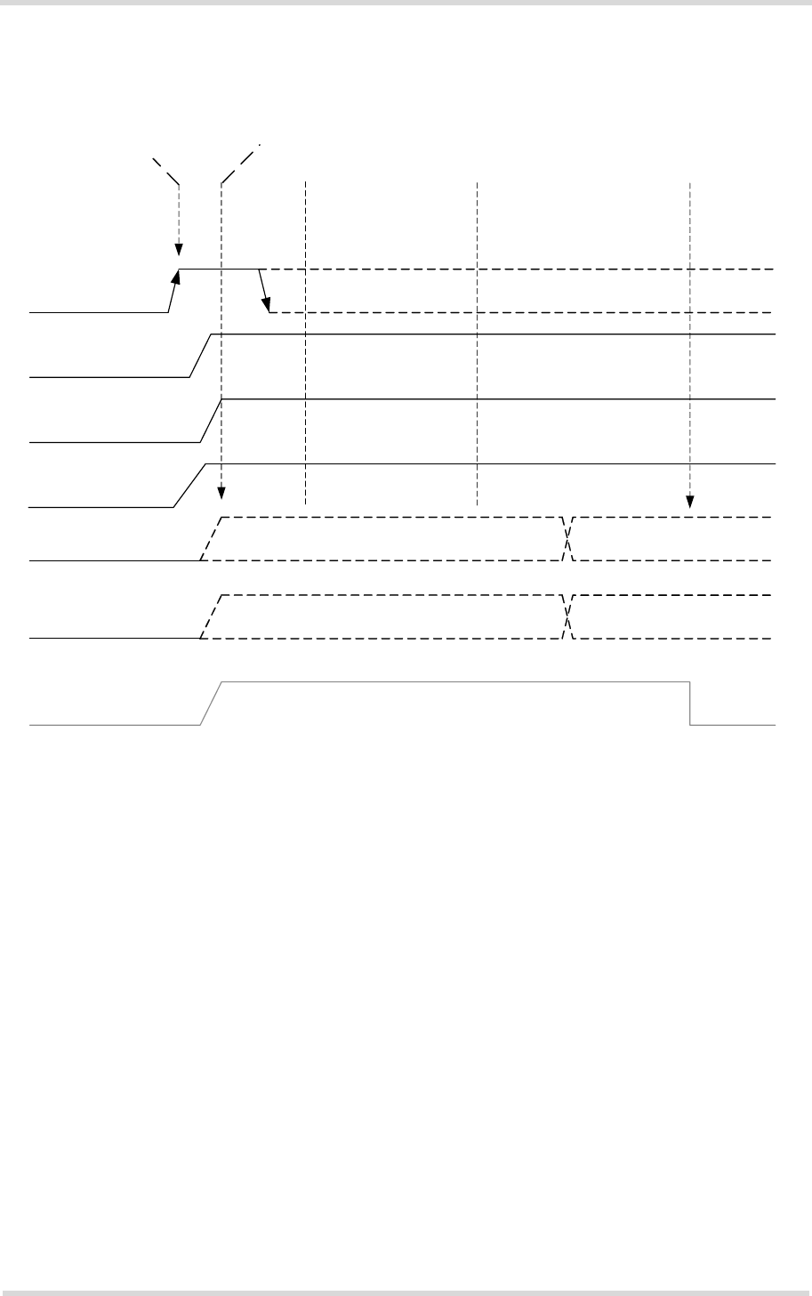
The following figure shows the startup behavior of the I2C interface. With an active state of the
ASC0 interface (i.e. CTS0 is at low level) the initialization of the I2C interface is also finished.
Figure 15: I2C startup behavior
I2CCLK
I2CDAT
Open drain
Open drain
(external pull up)
(external pull up)
CTS0
ON
EMERG_RST
Power supply active
Start up
Firmware
initialization
Command interface
initialization
Interface
active
V180
VCORE
Reset
state
Cinterion® ELS31-VA/ELS51-VA Hardware Interface Description
2.1 Application Interface
56
ELS31-VA_ELS51-VA_HID_v01.000 2017-01-04
Confidential / Preliminary
Page 38 of 106
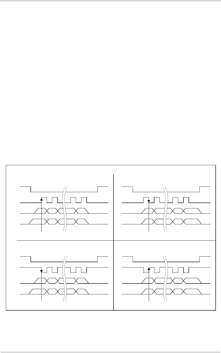
2.1.12 SPI Interface
The ELS31-VA/ELS51-VA GPIO interface lines can be configured as Serial Peripheral Inter-
face (SPI). The SPI is a synchronous serial interface for control and data transfer between
ELS31-VA/ELS51-VA and the external application. Only one application can be connected to
the SPI and the interface supports only master mode. The transmission rates are up to 6.5Mbit/
s. The SPI interface comprises the two data lines SPI_MOSI and SPI_MISO, the clock line
SPI_CLK a well as the chip select lines SPI_CS1 and SPI_CS2.
These two GPIO lines can be configured as SPI interface signals as follows: GPO26 -->
SPI_CS1 and GPIO27 --> SPI_CS2. The configuration is done by AT command (see [1]). It is
non-volatile and becomes active after a module restart.
To configure and activate the SPI interface use the AT^SSPI command. Detailed information
on the AT^SSPI command as well explanations on the SPI modes required for data transmis-
sion can be found in [1].
In general, SPI supports four operation modes. The modes are different in clock phase and
clock polarity. The module’s SPI mode can be configured by using the AT command AT^SSPI.
Make sure the module and the connected slave device works with the same SPI mode.
Figure 16 shows the characteristics of the four SPI modes. The SPI modes 0 and 3 are the most
common used modes. For electrical characteristics please refer to Table 2.
Figure 16: Characteristics of SPI modes
SPI MODE 0 SPI MODE 1
SPI MODE 2 SPI MODE 3
Clock phase
Clock polarity
SPI_CS
SPI_MOSI
SPI_CLK
SPI_MISO
SPI_CS
SPI_MOSI
SPI_CLK
SPI_MISO
SPI_CS
SPI_MOSI
SPI_CLK
SPI_MISO
SPI_CS
SPI_MOSI
SPI_CLK
SPI_MISO
Sample Sample
Sample Sample

Cinterion® ELS31-VA/ELS51-VA Hardware Interface Description
2.1 Application Interface
56
ELS31-VA_ELS51-VA_HID_v01.000 2017-01-04
Confidential / Preliminary
Page 39 of 106
2.1.13 Pulse Counter
The GPIO8 line can be configured as pulse counter line COUNTER (for GPIOs see Section
2.1.10). The pulse counter interface can be used, for example, as a clock - it is designed to
measure signals from 0 to 1000 pulses per second. Note that the pulse counter works in batch-
es of 8 pulses, i.e., the URC indicates the number of pulses counted in batches of 8 pulses. For
more information on how to use this feature see [1].
2.1.14 HSIC Interface (ELS51-VA Only)
The (USB) High Speed Inter Chip (HSIC) interface can be used between the module and an
external application processor, and is compliant to the High Speed USB 2.0 interface with
480Mbit/s. The maximum distance between module processor and external application proces-
sor should not exceed 100mm.
The HSIC interface comprises two signal lines (strobe - HSIC_STRB - and data - HSIC_DATA)
used in a source synchronous serial interface with a 240MHz clock to provide a 480Mbps USB
interface. The HSIC_STRB and HSIC_DATA lines are high-speed signals and should be rout-
ed as 50Ohm impedance traces. The trace length of these signals should be balanced to min-
imize timing skew and be no longer than 100mm.
The HSIC interface implementation complies with the USB HSIC standard “High-Speed Inter-
Chip USB Electrical Specification”, Version 1, September 23, 20071.
2.1.15 SDIO Interface (ELS51-VA Only)
The Secure Digital Input Output (SDIO) interface can be used to for instance connect an SD
card. The SDIO interface has the following features:
1. The USB specifications are ready for download on http://www.usb.org/developers/docs/usb20_docs/
Table 8: SDIO interface features
Feature Description/Value
Interface Type SDIO/SD1 (1 data line), SDIO/SD4 (4 data lines), MMC4 (4 data lines)
Voltage 1.8 V
DMA Mode SDMA / ADMA1 / ADMA2
Number of SLOTs 1
Implement DDR mode Yes
Card inserted status Yes
SDIOCLK frequency Default Mode: 23 MHz maximum
High Speed Mode: 46 MHz maximum
UHS-I Mode: 92 MHz
Max block length 2048 bytes
SDIO interrupt support Yes, support SDIO/SD1, SDIO/SD4 mode interrupts
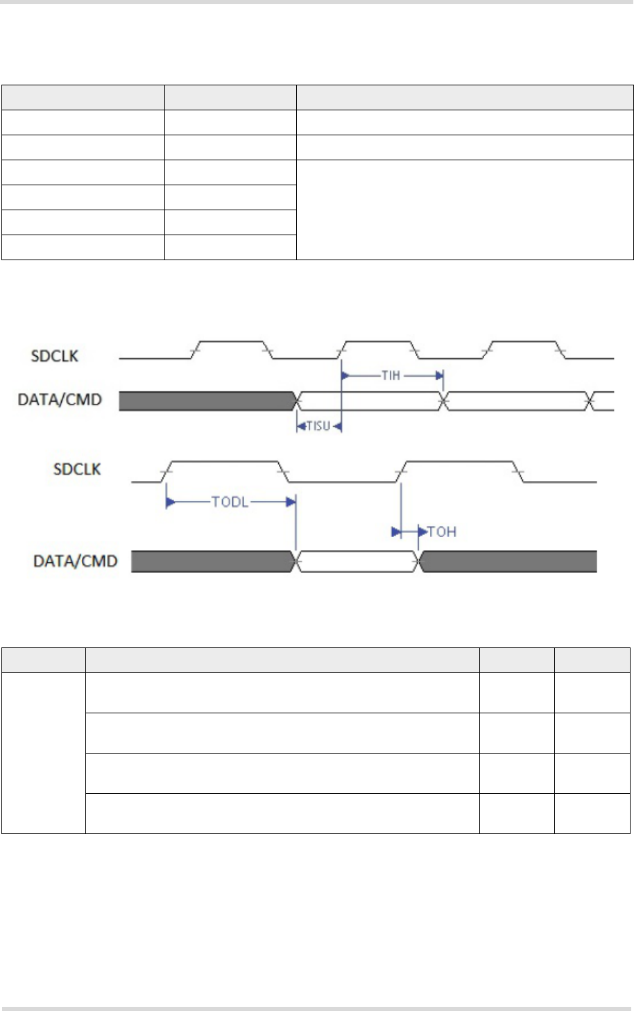
Cinterion® ELS31-VA/ELS51-VA Hardware Interface Description
2.1 Application Interface
56
ELS31-VA_ELS51-VA_HID_v01.000 2017-01-04
Confidential / Preliminary
Page 40 of 106
Table 9 lists the six SDIO interface lines:
Figure 17 illustrates the SDIO timings for data input and output, whereas the below Table 10
gives the actual timing values for the various speed modes.
Figure 17: SDIO interface timing diagrams (Input/Output)
Table 9: SDIO interface lines
Signal Direction Description
SDIOCLK Out SD master clock output to SD/MMC/SDIO device.
SDIOCMD I/O Command line.
SDIO0 I/O Data lines. Only SDIO0 carries data in 1-bit SD mode,
SDIO0..3 carry data in 4-bits mode.
SDIO interrupt is multiplexed with SDIO1.
SDIO1 I/O
SDIO2 I/O
SDIO3 I/O
Table 10: SDIO timings
Mode Parameter Minimum Maximum
Normal
speed
TISU
Input set-up time
5ns
TIH
Input hold time
5ns
TODL
Output delay time during Date Transfer Mode
0ns 14ns
TODL
Output delay time during Identification Mode
0ns 50ns
Cinterion® ELS31-VA/ELS51-VA Hardware Interface Description
2.1 Application Interface
56
ELS31-VA_ELS51-VA_HID_v01.000 2017-01-04
Confidential / Preliminary
Page 41 of 106
High speed TISU
Input set-up time
6ns
TIH
Input hold time
2ns
TODLY
Output delay time during Date Transfer Mode
0ns 14ns
TOH
Output hold time
2.5ns
USH-1 TISU
Input set-up time
3ns
TIH
Input hold time
0.8ns
TODLY
Output delay time during Date Transfer Mode (SDR12, SDR25)
0ns 14ns
TODLY
Output delay time during Date Transfer Mode (SDR50)
0ns 7.5ns
TOH
Output hold time
1.5ns
Table 10: SDIO timings
Mode Parameter Minimum Maximum
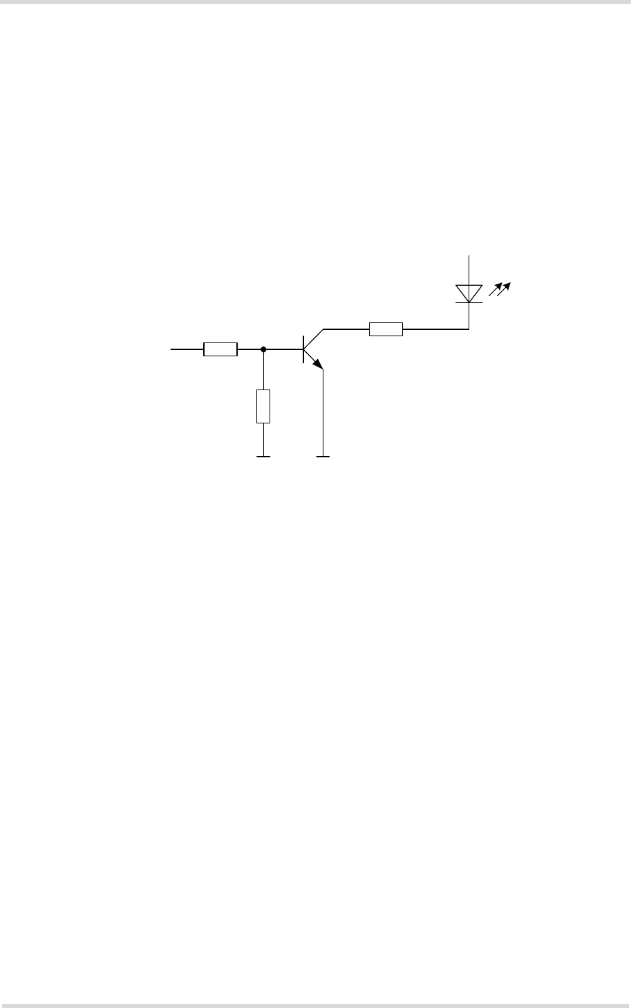
Cinterion® ELS31-VA/ELS51-VA Hardware Interface Description
2.1 Application Interface
56
ELS31-VA_ELS51-VA_HID_v01.000 2017-01-04
Confidential / Preliminary
Page 42 of 106
2.1.16 Control Signals
2.1.16.1 Status LED
The LED line can also be configured as GPO5 line, and can be used to drive a status LED that
indicates different operating modes of the module (for GPOs see Section 2.1.10). LED and
GPO functionality are mutually exclusive.
To take advantage of this function connect an LED to the LED/GPO5 line as shown in Figure
18.
Figure 18: Status signaling with LED driver
VCC
GPO5/
LED
LED
GNDGND
R1
R2
R3
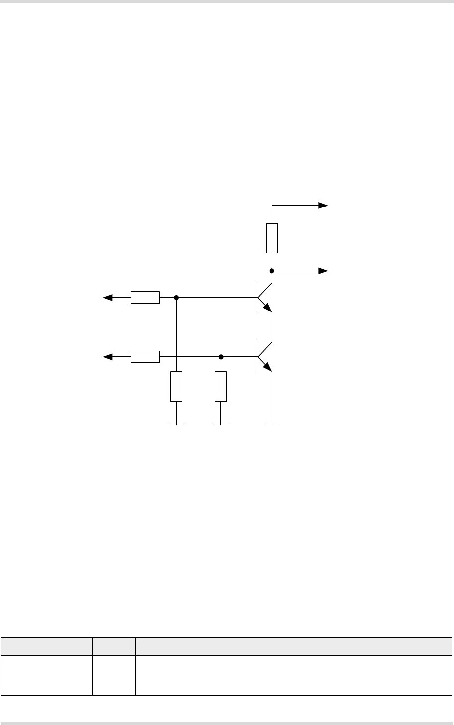
Cinterion® ELS31-VA/ELS51-VA Hardware Interface Description
2.1 Application Interface
56
ELS31-VA_ELS51-VA_HID_v01.000 2017-01-04
Confidential / Preliminary
Page 43 of 106
2.1.16.2 Power Indication Circuit
In Power Down mode the maximum voltage at any digital or analog interface line must not ex-
ceed +0.3V (see also Section 2.1.2.1). Exceeding this limit for any length of time might cause
permanent damage to the module.
It is therefore recommended to implement a power indication signal that reports the module’s
power state and shows whether it is active or in Power Down mode. While the module is in
Power Down mode all signals with a high level from an external application need to be set to
low state or high impedance state. The sample power indication circuit illustrated in Figure 19
denotes the module’s active state with a low signal and the module’s Power Down mode with
a high signal or high impedance state.
Figure 19: Power indication circuit
2.1.16.3 Host Wakeup
If no call, data or message transfer is in progress, the host may shut down its own USB inter-
face to save power. If a call or other request (URC’s, messages) arrives, the host can be noti-
fied of these events and be woken up again by a state transition of the ASC0 interface‘s RING0
line. This functionality should only be used with legacy USB applications not supporting the rec-
ommended USB suspend and resume mechanism as described in [5] (see also Section 2.1.3.2).
For more information on how to configure the RING0 line by AT^SCFG command see [1].
Possible RING0 line states are listed in Table 11.
Table 11: Host wakeup line
Signal I/O Description
RING0 O Inactive to active low transition:
0 = The host shall wake up
1 = No wake up request
22k
10k
100k
100k
4.7k
V180
VCORE
Power
indication
External
power supply
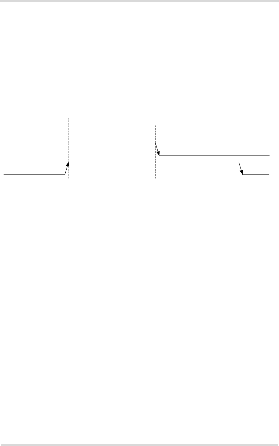
Cinterion® ELS31-VA/ELS51-VA Hardware Interface Description
2.1 Application Interface
56
ELS31-VA_ELS51-VA_HID_v01.000 2017-01-04
Confidential / Preliminary
Page 44 of 106
Figure 20 shows the described RING0 wake up mechanism:
• RING0 shall be high
• After a given programmable timeout with no activity on ASC0, RTS0 will be driven high and
the host will fall asleep if RING0 remains high (note: Host shall wait at least for one UART
character after RTS0 is driven high before entering sleep mode, to catch the last potential
character transmission over UART)
• The module will wake-up the host driving RING0 from high to low
• The Host will inform the module it is ready to receive over UART by driving RTS0 to low
Figure 20: Wake-up via RING0
RING0
Host wake-up event by
module
Host is ready to receive
over UART
RTS0
Host enters sleep mode
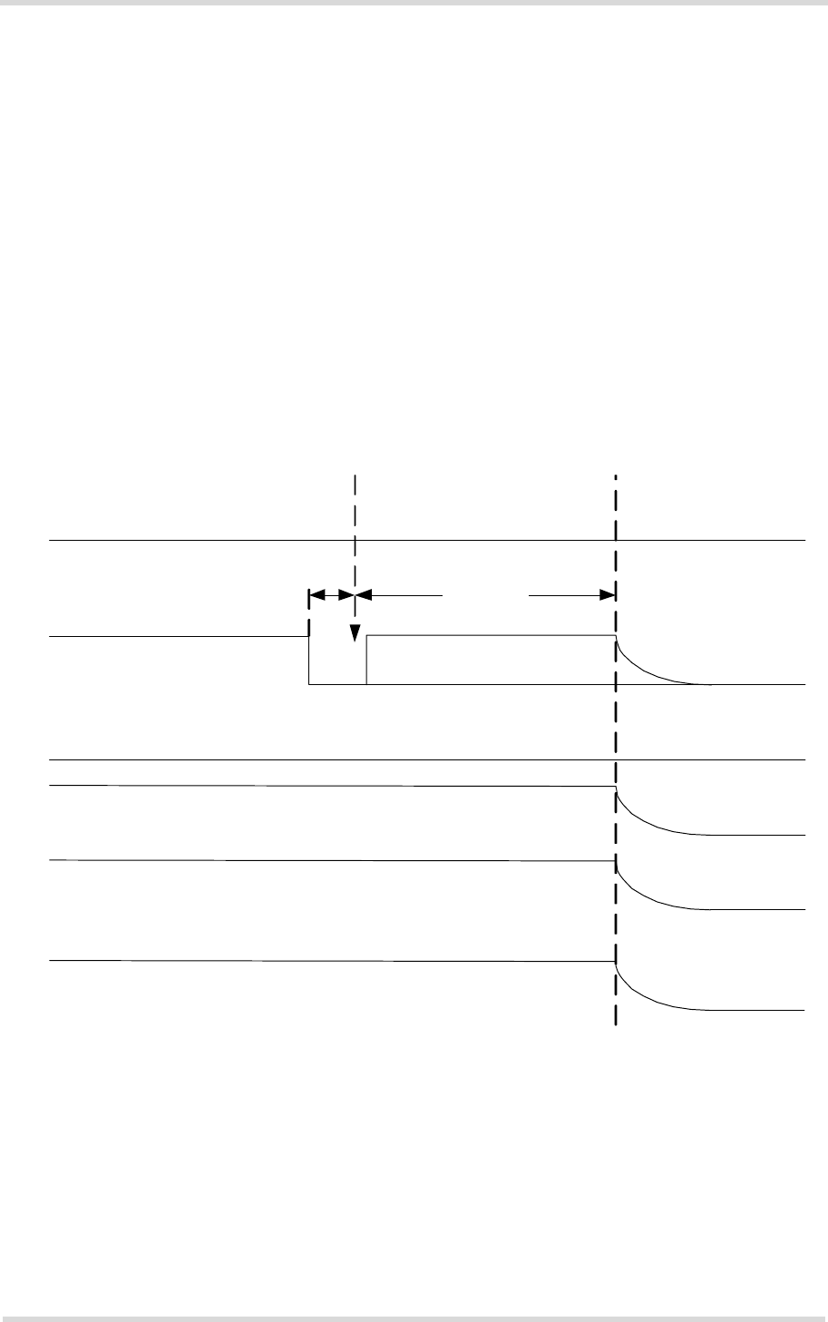
Cinterion® ELS31-VA/ELS51-VA Hardware Interface Description
2.1 Application Interface
56
ELS31-VA_ELS51-VA_HID_v01.000 2017-01-04
Confidential / Preliminary
Page 45 of 106
2.1.16.4 Fast Shutdown
The GPIO4 interface line can be configured as fast shutdown signal line FST_SHDN. The con-
figured FST_SHDN line is an active low control signal. Before setting the FST_SHDN line to
low, the ON signal should be set to low (see Figure 21).
By default, the fast shutdown feature is disabled. It has to be enabled using the AT command
AT^SCFG "MEShutdown/Fso". For details see [1].
If enabled, a low impulse of 10 milliseconds on the FST_SHDN line starts the fast shutdown
procedure.The fast shutdown procedure still finishes any data activities on the module‘s flash
file system, thus ensuring data integrity, but the module will no longer deregister gracefully from
the network. On-going flash access cycles (writing/deleting) will be finalized within less than
200 milliseconds. If the module is in power sleep mode, the 200 milliseconds maximum shut-
down time will start after the module wakes up from sleep mode.
Figure 21: Fast shutdown timing
Please note that if enabled, the normal software controlled shutdown using AT^SMSO will also
be a fast shutdown, i.e., without network deregistration. However, in this case no URCs includ-
ing shutdown URCs will be provided by the AT^SMSO command.
BATT+
ON
VCORE
V180
Fast shut down procedure Power down
EMERG_RST
FST_SHDN
max. 200ms
min. 10ms
Cinterion® ELS31-VA/ELS51-VA Hardware Interface Description
2.2 RF Antenna Interface
56
ELS31-VA_ELS51-VA_HID_v01.000 2017-01-04
Confidential / Preliminary
Page 46 of 106
2.2 RF Antenna Interface
The RF interface has an impedance of 50Ω. ELS31-VA/ELS51-VA is capable of sustaining a
total mismatch at the antenna line without any damage, even when transmitting at maximum
RF power.
The external antenna must be matched properly to achieve best performance regarding radi-
ated power, modulation accuracy and harmonic suppression. Antenna matching networks are
not included on the ELS31-VA/ELS51-VA module and should be placed in the host application
if the antenna does not have an impedance of 50Ω.
Regarding the return loss ELS31-VA/ELS51-VA provides the following values in the active
band:
2.2.1 Antenna Interface Specifications
ELS31-VA/ELS51-VA is equipped with two receiver ports. The sensitivity results according to
Table 13 are verified by using both antenna ports according to the recommendation given in
3GPP TS 36.521-1, Chapter 7.2. The sensitivity results also depend on the selected band-
width.
Table 12: Return loss in the active band
State of module Return loss of module Recommended return loss of application
Receive > 8dB > 12dB
Transmit not applicable > 12dB
Table 13: RF Antenna interface LTE
Parameter Conditions Min. Typical Max. Unit
LTE connectivity Band 4 and 13
Static Receiver input Sensi-
tivity @ ARP (ch. bandwidth
5MHz)
LTE Band 4 -99.3 -103 -- dBm
LTE Band 13 -99.3 -101 -- dBm
RF Power @ ARP with 50
Load
LTE Band 4 21 23 25 dBm
LTE Band 13 21 23 25 dBm
Cinterion® ELS31-VA/ELS51-VA Hardware Interface Description
2.2 RF Antenna Interface
56
ELS31-VA_ELS51-VA_HID_v01.000 2017-01-04
Confidential / Preliminary
Page 47 of 106
2.2.2 Antenna Installation
The antenna is connected by soldering the antenna pads (RF_OUT, pad #59 and DIV_ANT,
pad 56) its neighboring ground pads (GND, i.e., pads #55, #57, #58 and #60) directly to the
application’s PCB. The antenna pad is the antenna reference point (ARP) for ELS31-VA/ELS51-
VA. All RF data specified throughout this document is related to the ARP.
Figure 22: Antenna pads (bottom view)
The distance between the antenna RF pads and its neighboring GND pads has been optimized
for best possible impedance. On the application PCB, special attention should be paid to these
3 pads, in order to prevent mismatch.
The wiring of the antenna connection line, starting from the antenna pad to the application an-
tenna should result in a 50Ω line impedance. Line width and distance to the GND plane needs
to be optimized with regard to the PCB’s layer stack. Some examples are given in Section
2.2.3.
To prevent receiver desensitization due to interferences generated by fast transients like high
speed clocks on the application PCB, it is recommended to realize the antenna connection line
using embedded Stripline rather than Micro-Stripline technology. Please see Section 2.2.3.2
for an example.
For type approval purposes, the use of a 50Ω coaxial antenna connector (U.FL-R-SMT) might
be necessary. In this case the U.FL-R-SMT connector should be placed as close as possible
to ELS31-VA/ELS51-VA‘s antenna pad.
53
65
64
63
62
61
60
59
58
57
56
55
54
66
33
21
22
23
24
25
26
27
28
29
30
31
32
20
106
9291
9897969594
9089
85 86
93
74
99
87 88
8483
7978777675
8281
80
727170696867
105104103102101100
73
44
19181716151413121110987654321
343536373839404142434546474849505152
GND
GND
GND
GND
RF_OUT
DIV_ANT
251
250
252
245
249
248
247
246
Cinterion® ELS31-VA/ELS51-VA Hardware Interface Description
2.2 RF Antenna Interface
56
ELS31-VA_ELS51-VA_HID_v01.000 2017-01-04
Confidential / Preliminary
Page 48 of 106
2.2.3 RF Line Routing Design
2.2.3.1 RF Interface Signals Circuit Diagram Example
Figure 23 is a topology reference, and it is recommended not to deviate from this circuit for your
external application.
The RF inter-connects called RF Port 1 and RF Port 2 are examples only. Depending on the
RF antenna, the interfacing system will dictate the RF inter-connects.
Figure 23: RF interface signals example
Please be also aware of ESD protection required on the RF interface lines. ESD protection
might be utilized through the above pi-network (primarily intended for managing any additional
RF optimization needs), or by additional components in series with the pi-network illustrated
above. Please see Section 3.6.1 for further details.
Cinterion® ELS31-VA/ELS51-VA Hardware Interface Description
2.2 RF Antenna Interface
56
ELS31-VA_ELS51-VA_HID_v01.000 2017-01-04
Confidential / Preliminary
Page 49 of 106
2.2.3.2 Line Arrangement Examples
Several dedicated tools are available to calculate line arrangements for specific applications
and PCB materials - for example from http://www.polarinstruments.com/ (commercial software)
or from http://web.awrcorp.com/Usa/Products/Optional-Products/TX-Line/ (free software).
Embedded Stripline
This figure below shows a line arrangement example for embedded stripline with 65µm FR4
prepreg (type: 1080) and 710µm FR4 core (4-layer PCB).
Figure 24: Embedded Stripline with 65µm prepreg (1080) and 710µm core
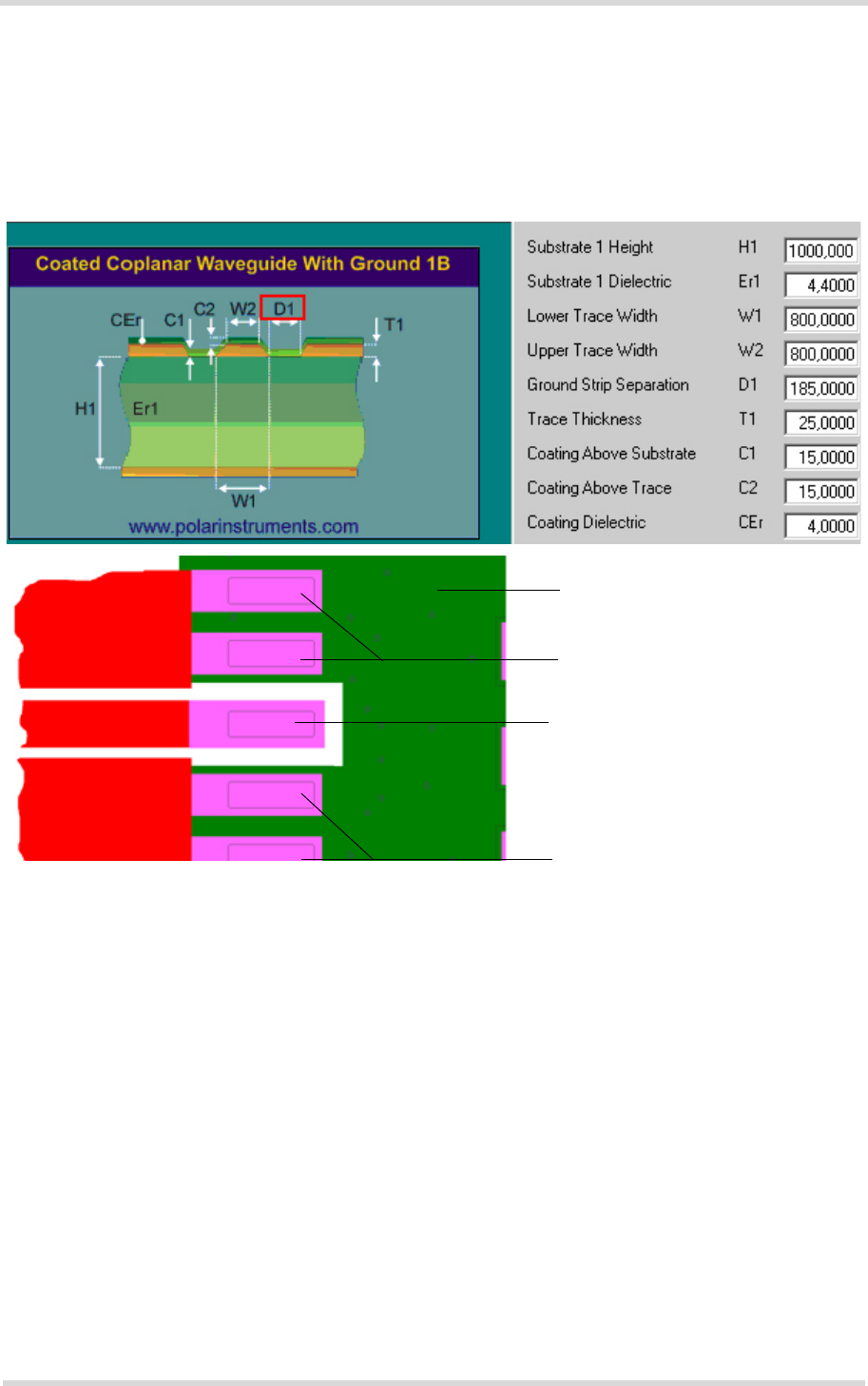
Cinterion® ELS31-VA/ELS51-VA Hardware Interface Description
2.2 RF Antenna Interface
56
ELS31-VA_ELS51-VA_HID_v01.000 2017-01-04
Confidential / Preliminary
Page 50 of 106
Micro-Stripline
This section gives two line arrangement examples for micro-stripline.
• Micro-Stripline on 1.0mm Standard FR4 2-Layer PCB
The following two figures show examples with different values for D1 (ground strip separa-
tion).
Figure 25: Micro-Stripline on 1.0mm standard FR4 2-layer PCB - example 1
Antenna line
Ground line
Ground line
Application board
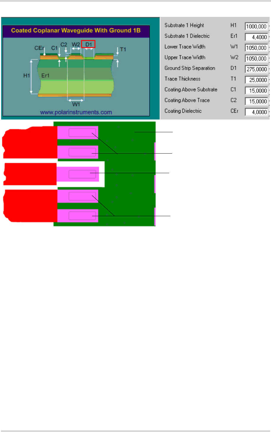
Cinterion® ELS31-VA/ELS51-VA Hardware Interface Description
2.2 RF Antenna Interface
56
ELS31-VA_ELS51-VA_HID_v01.000 2017-01-04
Confidential / Preliminary
Page 51 of 106
Figure 26: Micro-Stripline on 1.0mm Standard FR4 PCB - example 2
Antenna line
Ground line
Ground line
Application board
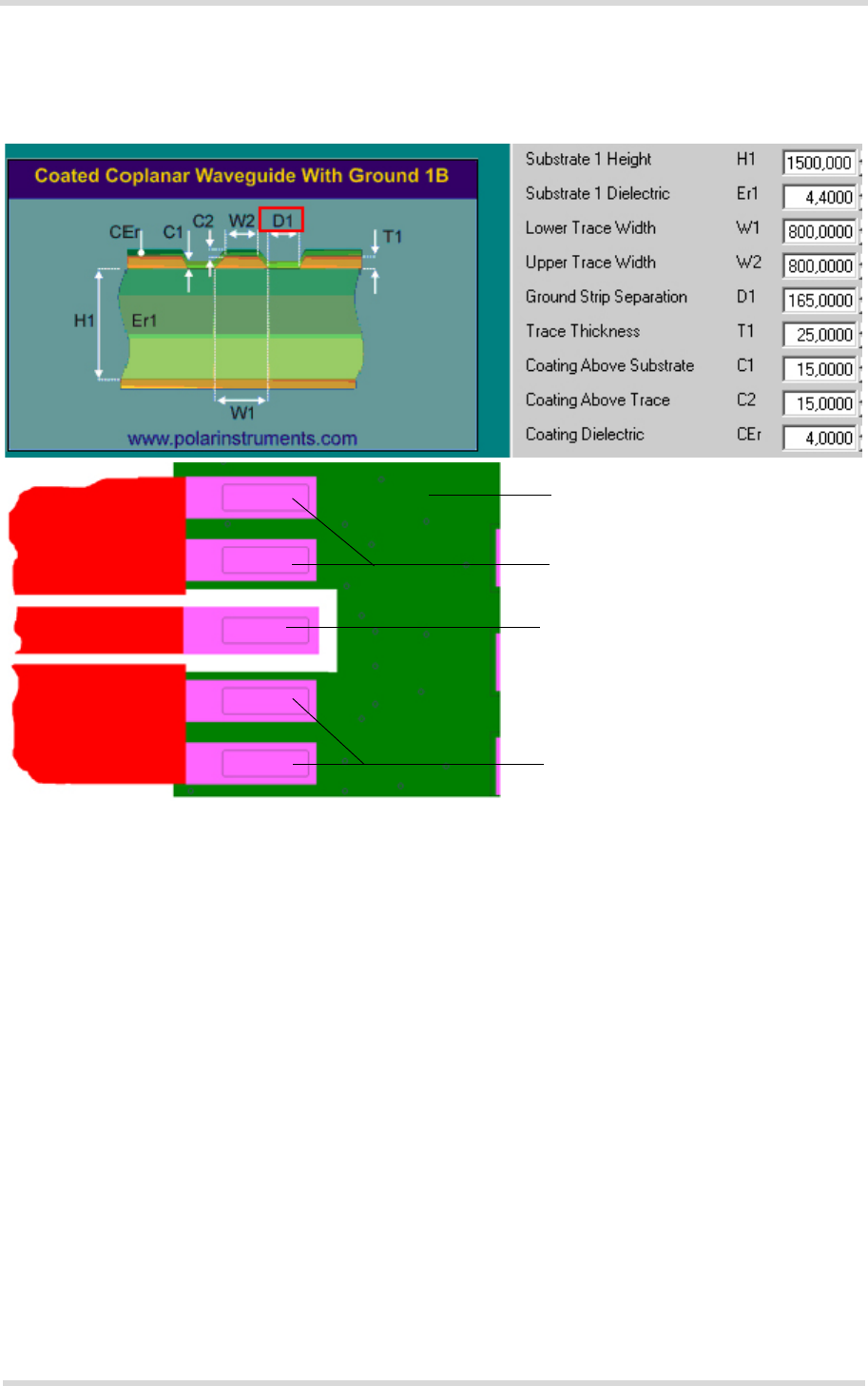
Cinterion® ELS31-VA/ELS51-VA Hardware Interface Description
2.2 RF Antenna Interface
56
ELS31-VA_ELS51-VA_HID_v01.000 2017-01-04
Confidential / Preliminary
Page 52 of 106
• Micro-Stripline on 1.5mm Standard FR4 2-Layer PCB
The following two figures show examples with different values for D1 (ground strip separa-
tion).
Figure 27: Micro-Stripline on 1.5mm Standard FR4 PCB - example 1
Antenna line
Ground line
Ground line
Application board
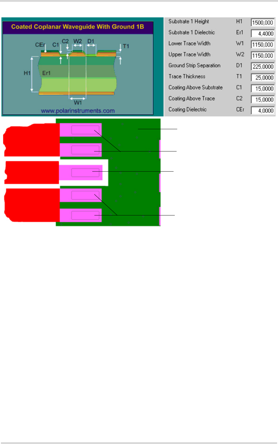
Cinterion® ELS31-VA/ELS51-VA Hardware Interface Description
2.2 RF Antenna Interface
56
ELS31-VA_ELS51-VA_HID_v01.000 2017-01-04
Confidential / Preliminary
Page 53 of 106
Figure 28: Micro-Stripline on 1.5mm Standard FR4 PCB - example 2
Antenna line
Ground line
Ground line
Application board

Cinterion® ELS31-VA/ELS51-VA Hardware Interface Description
2.3 Sample Application
56
ELS31-VA_ELS51-VA_HID_v01.000 2017-01-04
Confidential / Preliminary
Page 54 of 106
2.3 Sample Application
Figure 29 shows a typical example of how to integrate a ELS31-VA/ELS51-VA module with an
application. Usage of the various host interfaces depends on the desired features of the appli-
cation.
Because of the high RF field density inside the module, it cannot be guaranteed that no self
interference might occur, depending on frequency and the applications grounding concept. The
potential interferers may be minimized by placing small capacitors (47pF) at suspected lines
(e.g. RXD0, or ON).
While developing SMT applications it is strongly recommended to provide test points
for certain signals, i.e., lines to and from the module - for debug and/or test purposes.
The SMT application should allow for an easy access to these signals. For details on
how to implement test points see [4].
The EMC measures are best practice recommendations. In fact, an adequate EMC strategy for
an individual application is very much determined by the overall layout and, especially, the po-
sition of components. For example, mounting the internal acoustic transducers directly on the
PCB eliminates the need to use the ferrite beads shown in the sample schematic.
Depending on the micro controller used by an external application the module‘s digital input
and output lines may require level conversion. Section 2.3.2 shows a possible sample level
conversion circuit.
Note: ELS31-VA/ELS51-VA is not intended for use with cables longer than 3m.
Disclaimer
No warranty, either stated or implied, is provided on the sample schematic diagram shown in
Figure 29 and the information detailed in this section. As functionality and compliance with na-
tional regulations depend to a great amount on the used electronic components and the indi-
vidual application layout manufacturers are required to ensure adequate design and operating
safeguards for their products using ELS31-VA/ELS51-VA modules.
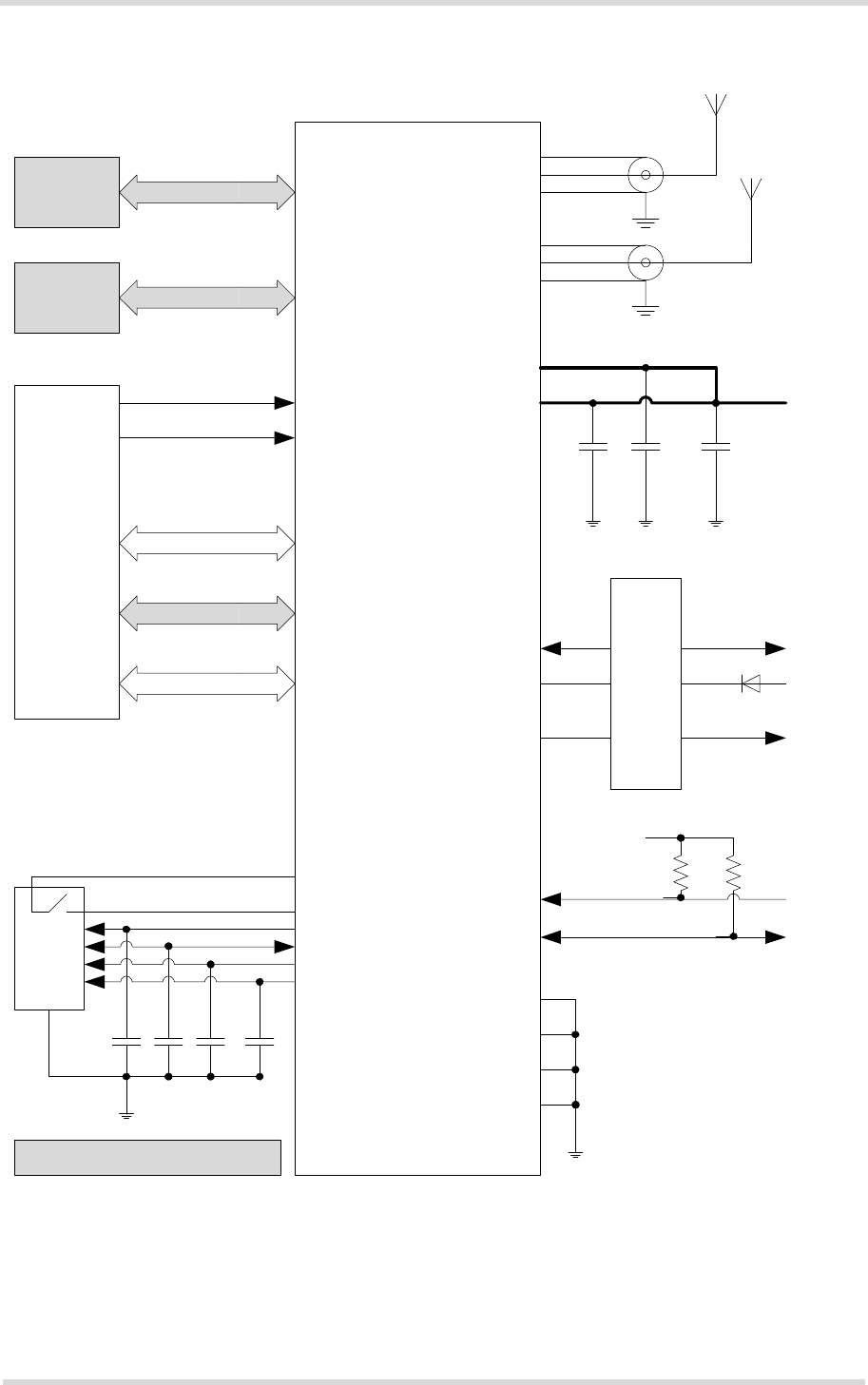
Cinterion® ELS31-VA/ELS51-VA Hardware Interface Description
2.3 Sample Application
56
ELS31-VA_ELS51-VA_HID_v01.000 2017-01-04
Confidential / Preliminary
Page 55 of 106
Figure 29: Schematic diagram of ELS31-VA/ELS51-VA sample application
ELS31/ELS51
Main Antenna
Div. Antenna
BATT+RF
BATT+BB
GPIOs
LED
COUNTER
I2CCLK
I2CDAT
GND
SDIO
HSIC
ON
FST_SHUTDOWN
ASC0
ASC1
USB
V180
CCIN
CCVCC
CCIO
CCRST
CCCLK
Power Supply
33pF 33pF + 150µF
Low ESR!
2k2 2k2
V180
Blocking
WiFi
µC
1nF 10pF10pF220nF
SIM
USB
Interfaces available only on ELS51
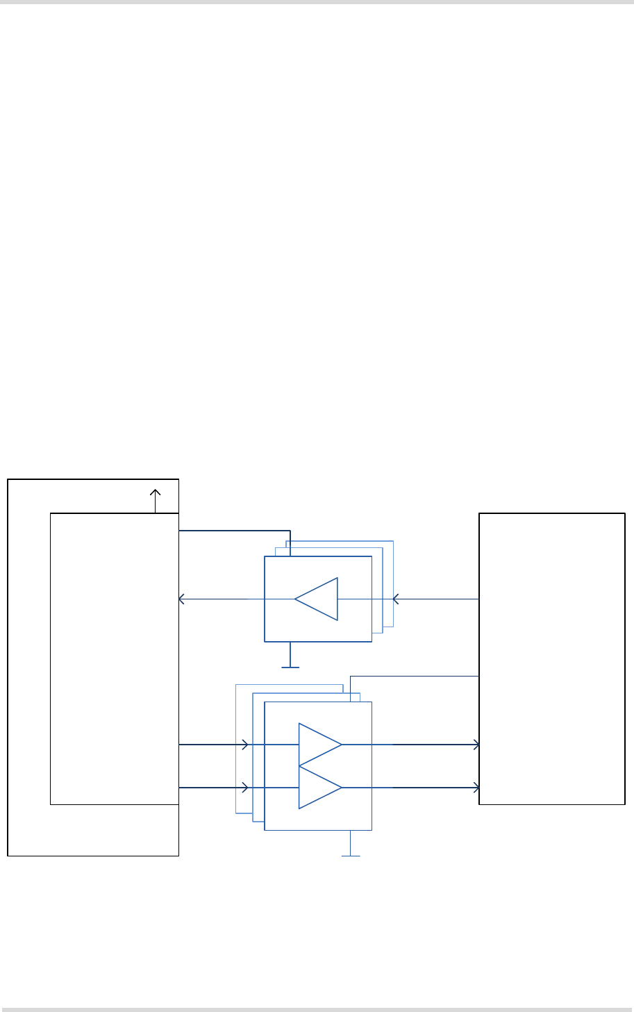
Cinterion® ELS31-VA/ELS51-VA Hardware Interface Description
2.3 Sample Application
56
ELS31-VA_ELS51-VA_HID_v01.000 2017-01-04
Confidential / Preliminary
Page 56 of 106
2.3.1 Prevent Back Powering
Because of the very low power consumption design, current flowing from any other source into
the module circuit must be avoided in any case, for example reverse current from high state
external control lines while the module is powered down. Therefore, the controlling application
must be designed to prevent reverse current flow. Otherwise there is the risk of undefined
states of the module during startup and shutdown or even of damaging the module.
A simple solution preventing back powering is the usage of V180 for level shifters, as Figure
30 shows.
While the module is in power down mode, V180 must have a level lower than 0.3V after
certain time. If this is not the case the module is fed back by the application interface - recog-
nizing such a fault state is possible by V180.
2.3.2 Sample Level Conversion Circuit
Depending on the micro controller used by an external application the module‘s digital input
and output lines (i.e., ASC0, ASC1 or GPIO lines) may require level conversion. The following
Figure 30 shows a sample circuit with recommended level shifters for an external application‘s
micro controller (with VLOGIC between 3.0V...3.6V). The level shifters can be used for digital
input and output lines with VOHmax=1.85V or VIHmax =1.85V.
Figure 30: Sample level conversion circuit
Note: Bidirectional level shifters without directions control signal are not suitable for RTS0 and
DCD0 as they may force the module into a wrong state while starting up.
5V tolerarant
Low level input
Low level input
Low level input
VCC
5V tolerant
VCC
E.g.,
74VHC1GT50
74LV1T34
E.g.,
74LVC2G34
NC7WZ16
External application
Micro controller
VLOGIC
(3.0V...3.6V)
Input lines,
e.g., µRXD, µCTS
Output lines,
e.g., µTXD, µRTS
V180 (1.8V)
Digital output lines,
e.g., RXDx, CTSx
Wireless module
Digital input lines,
e.g., TXDx, RTSx

Cinterion® ELS31-VA/ELS51-VA Hardware Interface Description
3 Operating Characteristics
76
ELS31-VA_ELS51-VA_HID_v01.000 2017-01-04
Confidential / Preliminary
Page 57 of 106
3 Operating Characteristics
3.1 Operating Modes
The table below briefly summarizes the various operating modes referred to throughout the
document.
Table 14: Overview of operating modes
Mode Function
Normal
opera-
tion
LTE IDLE No data transfer is in progress and the USB connection is suspended
by host (or is not present) and no active communication via ASC0/
ASC1. For power saving issues see Section 3.3. In IDLE mode, the
software can be active or in SLEEP state.
LTE DATA LTE data transfer in progress. Power consumption depends on network
settings and data transfer rate.
Power
Down
Normal shutdown after sending the power down command. Software is not active. Inter-
faces are not accessible. Operating voltage remains applied.
Airplane
mode
Airplane mode shuts down the radio part of the module, causes the module to log off from
the LTE network and disables all AT commands whose execution requires a radio connec-
tion.
Airplane mode can be controlled by AT command (see [1]).
In Airplane mode, the software can be active or in SLEEP state.
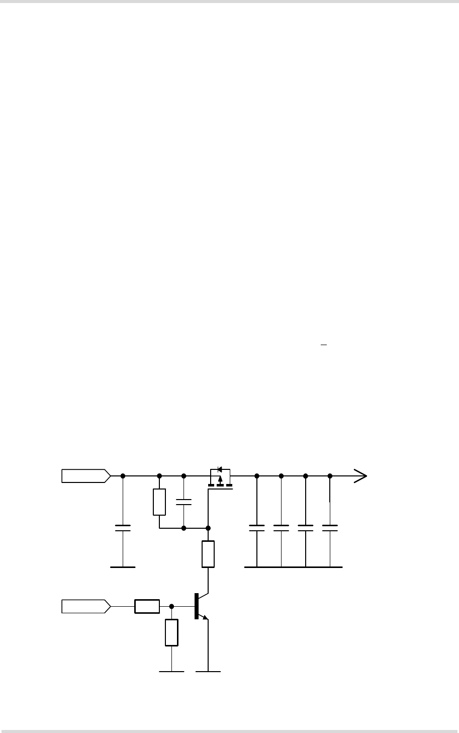
Cinterion® ELS31-VA/ELS51-VA Hardware Interface Description
3.2 Power Up/Power Down Scenarios
76
ELS31-VA_ELS51-VA_HID_v01.000 2017-01-04
Confidential / Preliminary
Page 58 of 106
3.2 Power Up/Power Down Scenarios
Do not turn on the ELS31-VA/ELS51-VA while it is beyond the safety limits of voltage and tem-
perature stated in Section 2.1.2.1. ELS31-VA/ELS51-VA will immediately switch off when these
conditions are detected. In extreme cases this can cause permanent damage to the module.
3.2.1 Turn on ELS31-VA/ELS51-VA
ELS31-VA/ELS51-VA can be turned on as described in the following sections:
• Connecting the operating voltage BATT_BB and BATT_RF (see Section 3.2.1.1).
• Hardware driven switch on by ON line: Starts Normal mode (see Section 3.2.1.2).
After startup or restart, the module will send the URC ^SYSSTART that notifies the host appli-
cation that the first AT command can be sent to the module (see also [1]).
3.2.1.1 Connecting ELS31-VA/ELS51-VA BATT Lines
Figure 31 shows sample external application circuits that allow to connect (and also to tempo-
rarily disconnect) the module‘s BATT_BB and BATT_RF lines from the external application‘s
power supply.
Figure 31 illustrates the application of power using an externally controlled microcontroller. The
transistor T2 mentioned in Figure 31 should have an RDS_ON value < 50m in order to minimize
voltage drops.
Such circuits could be useful to maximize power savings for battery driven applications or to
completely switch off and restart the module after a firmware update.
After connecting the BATT_BB and BATT_RF lines the module can then be (re-)started as de-
scribed in Section 3.2.1.2.
Figure 31: Sample circuit for applying power using an external µC
3.8V
Module
Place C2-C5 close to moduleµcontroller
ENABLE
BATT_BB/RF
BATT_IN
C1
100nF
C2 47µF,X5R
C3 47µF,X5R
C4 47µF,X5R
C5 47µF,X5R
C6 47µF,X5R
R1
100k
R2
100k
R3
100k
R6
10k
T1
BC857
T2
IRML6401
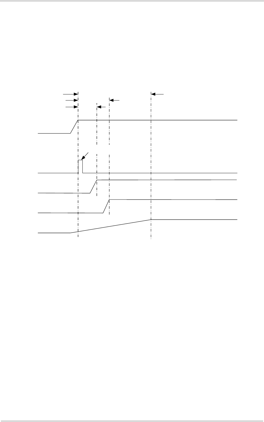
Cinterion® ELS31-VA/ELS51-VA Hardware Interface Description
3.2 Power Up/Power Down Scenarios
76
ELS31-VA_ELS51-VA_HID_v01.000 2017-01-04
Confidential / Preliminary
Page 59 of 106
3.2.1.2 Switch on ELS31-VA/ELS51-VA Using ON Signal
When the operating voltage BATT_BB is applied, ELS31-VA/ELS51-VA can be switched on by
means of the ON signal.
The ON signal is an edge triggered signal. The module starts into normal mode on detecting a
rising edge at the ON signal. The subsequent high level at the ON signal should last for at least
100µs. Note that if the ON signal is set to high before BATT_BB is applied, ELS31-VA/ELS51-
VA may not start up correctly.
Figure 32: ON timing
The module can also start automatically and immediately after applying the VBATT by connect-
ing the ON pad to BATT_BB for a so-called auto start mode. If ON is connected to BATT_BB,
and the module is switched off (e.g. by calling AT^SMSO), it will immediately restart.
For the auto start mode, it is recommended to set a pull-up resistor of maximum TBD.kOhm
between the ON circuit and the BATT_BB power supply.
Note: If during a power cycle or voltage drop the BATT_BB voltage level does not drop below
0.5V, it may happen that the module can no longer start up properly, because its reset condition
was not reached. This scenario can happen, if the BATT_BB supply is decoupled by big capac-
itors – with a slow discharge after a sudden power drop. So, please make sure to keep the pow-
er off state long enough for the capacitors to discharge below 0.5V. As a workaround it is
recommended to reset the module with EMERG_RST after startup (see also Section 3.2.2.2).
If an automatic module startup is configured for the module, i.e., the ON signal is connected to
BATT_BB, then the EMERG_RST signal may be generated automatically – using an external
voltage detector - when the BATT_BB voltage does reach the valid operating voltage range.
BATT_BB
ON
V180
VCORE
> 250µs
> 250µs
EMERG_RST
High level 100µs min.
~ 100ms
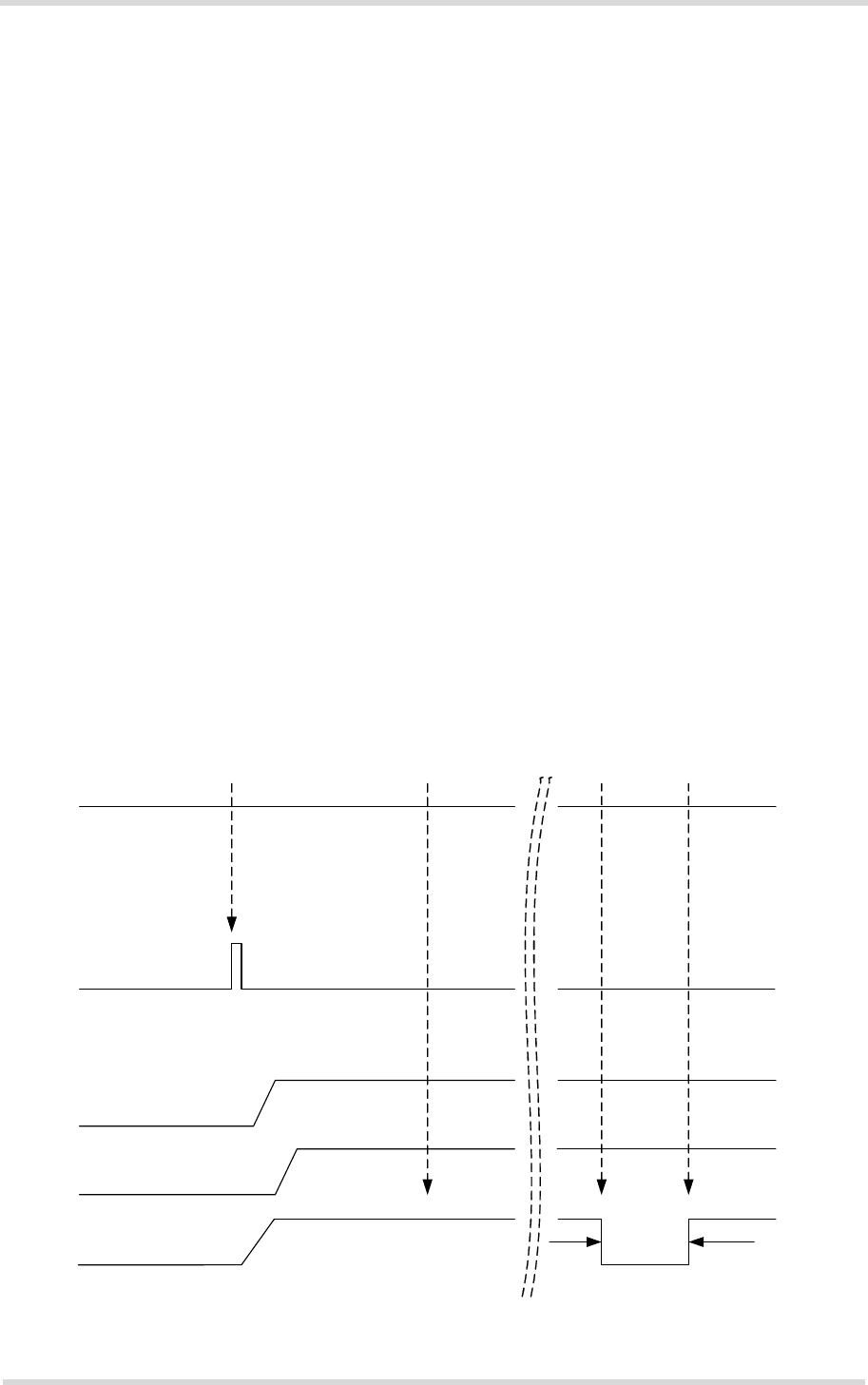
Cinterion® ELS31-VA/ELS51-VA Hardware Interface Description
3.2 Power Up/Power Down Scenarios
76
ELS31-VA_ELS51-VA_HID_v01.000 2017-01-04
Confidential / Preliminary
Page 60 of 106
3.2.2 Restart ELS31-VA/ELS51-VA
After startup ELS31-VA/ELS51-VA can be re-started as described in the following sections:
• Software controlled reset by AT+CFUN command: Starts Normal mode (see Section
3.2.2.1)
• Hardware controlled reset by EMERG_RST line: Starts Normal mode (see Section 3.2.2.2)
3.2.2.1 Restart ELS31-VA/ELS51-VA via AT+CFUN Command
To reset and restart the ELS31-VA/ELS51-VA module use the command AT+CFUN. See [1]
for details.
3.2.2.2 Restart ELS31-VA/ELS51-VA Using EMERG_RST
The EMERG_RST signal is internally connected to the central GSM processor. A low level for
more than 10 milliseconds sets the processor and with it all the other signal pads to their re-
spective reset state. The reset state is described in Section 3.2.3 as well as in the figures show-
ing the startup behavior of an interface.
After releasing the EMERG-RST line, i.e., with a change of the signal level from low to high,
the module restarts. The other signals continue from their reset state as if the module was
switched on by the ON signal.
Figure 33: Emergency restart timing
BATT_BB
ON
EMERG_RST
VCORE
V180
>10ms
System
started
System
started again
Reset
state
Ignition

Cinterion® ELS31-VA/ELS51-VA Hardware Interface Description
3.2 Power Up/Power Down Scenarios
76
ELS31-VA_ELS51-VA_HID_v01.000 2017-01-04
Confidential / Preliminary
Page 61 of 106
It is recommended to control this EMERG_RST line with an open collector transistor or an open
drain field-effect transistor.
Note: It is necessary to trigger EMERG_RST after a module turn off by a sudden (incomplete)
power drop, and before using ON to restart the module (see also Section 3.2.1.2).
Caution: Generally, use the EMERG_RST line only when, due to serious problems, the soft-
ware is not responding for more than 5 seconds. Pulling the EMERG_RST line causes the loss
of all information stored in the volatile memory. Therefore, this procedure is intended only for
use in case of emergency, e.g. if ELS31-VA/ELS51-VA does not respond, if restart or shutdown
via AT command fails.

Cinterion® ELS31-VA/ELS51-VA Hardware Interface Description
3.2 Power Up/Power Down Scenarios
76
ELS31-VA_ELS51-VA_HID_v01.000 2017-01-04
Confidential / Preliminary
Page 62 of 106
3.2.3 Signal States after First Startup
Table 15 lists the states each interface signal passes through during reset and first firmware
initialization. For further firmware startup initializations the values may differ because of differ-
ent GPIO line configurations.
The reset state is reached with the rising edge of an internal reset line - either with a normal
module startup after about 26 milliseconds (see Section 3.2.1) or after a restart (see Section
3.2.2). After the reset state has been reached the firmware initialization state begins. The firm-
ware and command interface initialization is completed as soon as the ASC0 interface line
CTS0 has turned low (see Section 2.1.4). Now, the module is ready to receive and transmit data.
Abbreviations used in above Table 15:
Table 15: Signal states
Signal name Default functionality Reset state First start up configuration
CCIO I O / L
CCRST I O / L
CCCLK O / L O / L
CCIN I I / PD
RXD0 I / PU O / H
TXD0 I I
CTS0 I O / H
RTS0 I I / PD
GPIO1/DTR0 DTR0 T / PD I / PU
GPIO2/DCD0 DCD0 T / PD O
GPIO3/DSR0 DSR0 T / PD O
GPIO4/FST_SHDN GPIO4 I / PD I / PU
GPO5/LED LED I / PD O
GPIO6 GPIO6 I / PD I / PD
GPIO7 GPIO7 I / PU I / PD
GPIO8/COUNTER GPIO8 I I / PD
GPIO16/RXD1 GPIO16 I I / PU
GPIO17/TXD1 GPIO17 I /PU I / PU
GPIO18/RTS1 GPIO18 I /PU I / PU
GPIO19/CTS1 GPIO19 I /PU I / PU
GPIO20/PCM_I2S_OUT GPIO20 I I / PD
GPIO21/PCM_I2S_IN GPIO21 I I / PD
GPIO22/PCM_I2S_FSC GPIO22 I I / PD
GPO23/PCM_I2S_CLK GPO23 I O / L
GPIO24/RING0 RING0 T / PD O
GPIO25 GPIO25 I I / PD
GPO26/SPI_CS1 GPO26 I O
GPIO27/SPI_CS2 GPIO27 I I / PD
I2CCLK I / PD T / OD
I2CDAT I / PD T / OD
L = Low level
H = High level
T = Tristate
I = Input
O = Output
OD = Open Drain
PD = Pull down
PU = Pull up
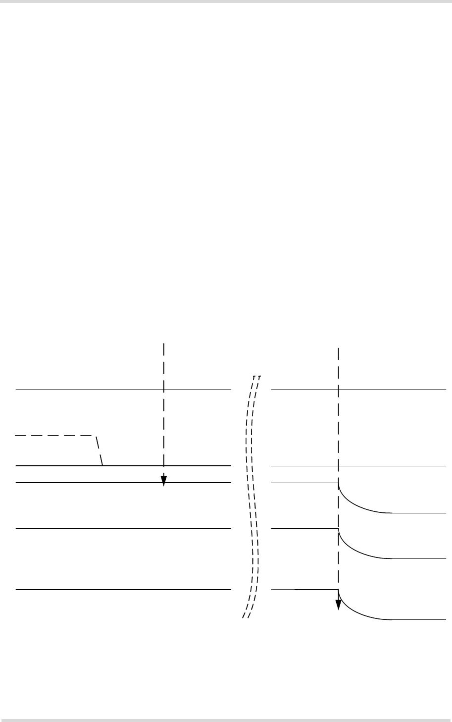
Cinterion® ELS31-VA/ELS51-VA Hardware Interface Description
3.2 Power Up/Power Down Scenarios
76
ELS31-VA_ELS51-VA_HID_v01.000 2017-01-04
Confidential / Preliminary
Page 63 of 106
3.2.4 Turn off ELS31-VA/ELS51-VA
To switch the module off the following procedures may be used:
•Software controlled shutdown procedure: Software controlled by sending an AT command
over the serial application interface. See Section 3.2.4.1.
•Hardware controlled shutdown procedure: Hardware controlled by employing the
FST_SHDN line. See Section 2.1.16.4.
•Automatic shutdown (software controlled): See Section 3.2.5
- Takes effect if ELS31-VA/ELS51-VA board temperature exceeds a critical limit.
3.2.4.1 Switch off ELS31-VA/ELS51-VA Using AT Command
The best and safest approach to powering down ELS31-VA/ELS51-VA is to issue the appropriate
AT command. This procedure lets ELS31-VA/ELS51-VA log off from the network and allows the
software to enter into a secure state and safe data before disconnecting the power supply. The
mode is referred to as Power Down mode. In this mode. Before issueing the switch off AT com-
mand, the ON signal should be set to low (see Figure 34). Otherwise there might be back pow-
ering at the ON line in Power Down mode.
While ELS31-VA/ELS51-VA is in Power Down mode the application interface is switched off and
must not be fed from any other voltage source. Therefore, your application must be designed
to avoid any current flow into any digital pads of the application interface.
Figure 34: Switch off behavior
BATT+
ON
VCORE
V180
AT^SMSO System power down procedure Power down
EMERG_RST

Cinterion® ELS31-VA/ELS51-VA Hardware Interface Description
3.2 Power Up/Power Down Scenarios
76
ELS31-VA_ELS51-VA_HID_v01.000 2017-01-04
Confidential / Preliminary
Page 64 of 106
3.2.5 Automatic Shutdown
Automatic shutdown takes effect if the following event occurs:
• The ELS31-VA/ELS51-VA board is exceeding the critical limits of overtemperature or under-
temperature (see Section 3.2.5.1)
• Undervoltage or overvoltage is detected (see Section 3.2.5.2 and Section 3.2.5.3)
The automatic shutdown procedure is equivalent to the power-down initiated with an AT com-
mand, i.e. ELS31-VA/ELS51-VA logs off from the network and the software enters a secure state
avoiding loss of data.
3.2.5.1 Thermal Shutdown
The board temperature is constantly monitored by an internal NTC resistor located on the PCB.
The values detected by the NTC resistor are measured directly on the board and therefore, are
not fully identical with the ambient temperature.
Each time the board temperature goes out of range or back to normal, ELS31-VA/ELS51-VA in-
stantly displays an alert (if enabled).
• URCs indicating the level "1" or "-1" allow the user to take appropriate precautions, such as
protecting the module from exposure to extreme conditions. The presentation of the URCs
depends on the settings selected with the AT^SCTM write command (for details see [1]):
AT^SCTM=1: Presentation of URCs is always enabled.
AT^SCTM=0 (default): Presentation of URCs is enabled during the 2 minute guard period
after start-up of ELS31-VA/ELS51-VA. After expiry of the 2 minute guard period, the presen-
tation of URCs will be disabled, i.e. no URCs with alert levels "1" or ''-1" will be generated.
• URCs indicating the level "2" or "-2" are instantly followed by an orderly shutdown. The pre-
sentation of these URCs is always enabled, i.e. they will be output even though the factory
setting AT^SCTM=0 was never changed.
The maximum temperature ratings are stated in Section 3.5. Refer to Table 16 for the associ-
ated URCs.
Table 16: Temperature dependent behavior
Sending temperature alert (2min after module start-up, otherwise only if URC presentation enabled)
^SCTM_B: 1 Board close to overtemperature limit.
^SCTM_B: -1 Board close to undertemperature limit.
^SCTM_B: 0 Board back to non-critical temperature range.
Automatic shutdown (URC appears no matter whether or not presentation was enabled)
^SCTM_B: 2 Alert: Board equal or beyond overtemperature limit. ELS31-VA/ELS51-VA switches
off.
^SCTM_B: -2 Alert: Board equal or below undertemperature limit. ELS31-VA/ELS51-VA switches
off.

Cinterion® ELS31-VA/ELS51-VA Hardware Interface Description
3.2 Power Up/Power Down Scenarios
76
ELS31-VA_ELS51-VA_HID_v01.000 2017-01-04
Confidential / Preliminary
Page 65 of 106
3.2.5.2 Undervoltage Shutdown
The undervoltage shutdown threshold is the specified minimum supply voltage VBATT+ given in
Table 2. When the average supply voltage measured by ELS31-VA/ELS51-VA approaches the
undervoltage shutdown threshold (i.e., 0.05V offset) the module will send the following URC:
^SBC: Undervoltage Warning
The undervoltage warning is sent only once - until the next time the module is close to the un-
dervoltage shutdown threshold.
If the voltage continues to drop below the specified undervoltage shutdown threshold, the mod-
ule will send the following URC:
^SBC: Undervoltage Shutdown
This alert is sent only once before the module shuts down cleanly without sending any further
messages.
This type of URC does not need to be activated by the user. It will be output automatically when
fault conditions occur.
Note: For battery powered applications it is strongly recommended to implement a BATT+ con-
necting circuit as described in Section 3.2.1.1 in order to not only be able save power, but also
to restart the module after an undervoltage shutdown where the battery is deeply discharged.
Also note that the undervoltage threshold is calculated for max. 400mV voltage drops during
transmit burst. Power supply sources for external applications should be designed to tolerate
400mV voltage drops without crossing the lower limit of 3.3 V. For external applications oper-
ating at the limit of the allowed tolerance the default undervoltage threshold may be adapted
by subtracting an offset. For details see [1]: AT^SCFG= "MEShutdown/sVsup/threshold".
3.2.5.3 Overvoltage Shutdown
The overvoltage shutdown threshold is the specified maximum supply voltage VBATT+ given in
Table 2. When the average supply voltage measured by ELS31-VA/ELS51-VA approaches the
overvoltage shutdown threshold (i.e., 0.05V offset) the module will send the following URC:
^SBC: Overvoltage Warning
The overvoltage warning is sent only once - until the next time the module is close to the over-
voltage shutdown threshold.
If the voltage continues to rise above the specified overvoltage shutdown threshold, the module
will send the following URC:
^SBC: Overvoltage Shutdown
This alert is sent only once before the module shuts down cleanly without sending any further
messages.
This type of URC does not need to be activated by the user. It will be output automatically when
fault conditions occur.
Keep in mind that several module components are directly linked to BATT+ and, therefore, the
supply voltage remains applied at major parts of ELS31-VA/ELS51-VA. Especially the power
amplifier linked to BATT+RF is very sensitive to high voltage and might even be destroyed.
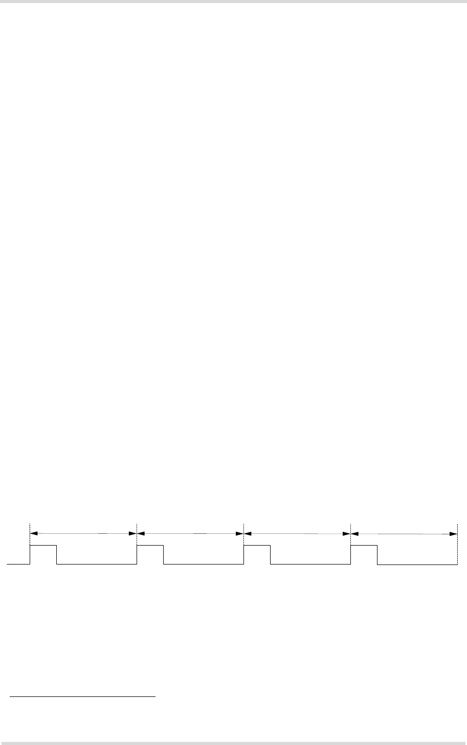
Cinterion® ELS31-VA/ELS51-VA Hardware Interface Description
3.3 Power Saving
76
ELS31-VA_ELS51-VA_HID_v01.000 2017-01-04
Confidential / Preliminary
Page 66 of 106
3.3 Power Saving
ELS31-VA/ELS51-VA can be configured in two ways to control power consumption:
• Being set by configuration, it is possible to specify a so-called power saving mode for the
module (for details on the command see [1]). The module's UART interfaces (ASC0 and
ASC1) are then deactivated and will only periodically be activated to be able to listen to net-
work paging messages as described in Section 3.3.1. See Section 3.3.2 for a description
of how to immediately wake up ELS31-VA/ELS51-VA again using RTS0.
Note: RTS0/RTS1 must to be set to high before the ELS31-VA/ELS51-VA can change into
power saving mode. Also note that the AT^SPOW setting has no effect on the USB inter-
face. As long as the USB connection is active, the module will not change into its SLEEP
state to reduce its functionality to a minimum and thus minimizing its current consumption.
To enable switching into SLEEP mode, the USB connection must therefore either not be
present at all or the USB host must bring its USB interface into Suspend state. Also, VUS-
B_IN should always be kept enabled for this functionality. See “Universal Serial Bus Spec-
ification Revision 2.0”1 for a description of the Suspend state.
• Being triggered by LTE network protocol while attached to LTE networks
3.3.1 Power Saving while Attached to LTE Networks
The power saving possibilities while attached to a LTE network depend on the paging timing
cycle of the base station.
During normal LTE operation, i.e., the module is connected to a LTE network, the duration of
a power saving period varies. It may be calculated using the following formula:
t = DRX Cycle Value* 10 ms
DRX (Discontinuous Reception) value in LTE networks is any of the four values: 32, 64, 128
and 256, thus resulting in power saving intervals between 0.32 and 2.56 seconds. The DRX
value of the base station is assigned by the LTE network operator.
In the pauses between listening to paging messages, the module resumes power saving, as
shown in Figure 35.
Figure 35: Power saving and paging in LTE networks
The varying pauses explain the different potential for power saving. The longer the pause the
less power is consumed.
Generally, power saving depends on the module’s application scenario and may differ from the
above mentioned normal operation. The power saving interval may be shorter than 0.64 sec-
onds or longer than 5.12 seconds.
1. The specification is ready for download on http://www.usb.org/developers/docs/
Power SavingPaging
DRX Cycle
0.32 - 2.56s
Power SavingPaging
DRX Cycle
0.32 - 2.56s
Power SavingPaging
DRX Cycle
0.32 - 2.56s
Power SavingPaging
DRX Cycle
0.32 - 2.56s
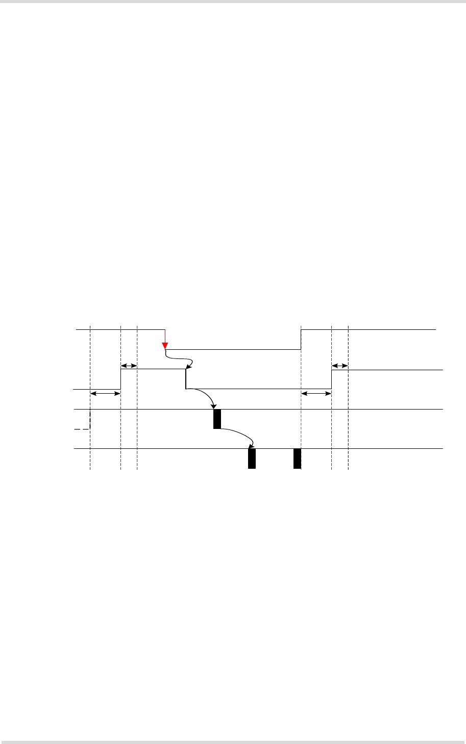
Cinterion® ELS31-VA/ELS51-VA Hardware Interface Description
3.3 Power Saving
76
ELS31-VA_ELS51-VA_HID_v01.000 2017-01-04
Confidential / Preliminary
Page 67 of 106
3.3.2 Wake-up via RTS0/RTS1
RTS0/RTS1 can be used to wake up ELS31-VA/ELS51-VA from SLEEP mode configured with
AT command. Assertion of either RTS0 or RTS1 (i.e., toggle from inactive high to active low)
serves as wake up event, thus allowing an external application to almost immediately terminate
power saving. After RTS0/RTS1 assertion, the CTS0/CTS1 line signals module wake up, i.e.,
readiness of the AT command interface. It is therefore recommended to enable RTS/CTS flow
control (default setting).
Figure 36 shows the described RTS0/RTS1 wake up mechanism.
• RTS0/RTS1 must be high.
• After a given programmable timeout (100ms up to 10s, default 5s) with no activity on ASC0
and ASC1 (and no data to transmit by module to host in Linux /dev/tty driver), CTS0/CTS1
will be driven high.
• After a 2nd timeout (equal or greater than the duration needed to receive one character at
UART baudrate; ex: ~1.05ms for 10bit @ 9600baud), and while RTS0/RTS1 remains high
(which means an external application does not request the module to wake up), the module
will enter sleep mode.
• Now, the host can wake-up the module driving RTS0/RTS1 from high to low.
• Module will inform the host it is ready to receive over UART by driving CTS0/CTS1 to low.
Figure 36: Wake-up via RTS0/RTS1
Note: RTS0/RTS1 has to be high for ELS31-VA/ELS51-VA to be able to change into SLEEP
mode.
RTS0/RTS1
CTS0/CTS1
TXD0/TXD1
RXD0/RXD1
AT command
Reply URC
RTS assertion (falling edge)
W ake up from SLEEP m ode R e turn to S L E E P
mode
RTS back high
<1.05ms
100ms
to1 0 s
100m s
to10s
<1.05ms
SLEEP
mode

Cinterion® ELS31-VA/ELS51-VA Hardware Interface Description
3.4 Power Supply
76
ELS31-VA_ELS51-VA_HID_v01.000 2017-01-04
Confidential / Preliminary
Page 68 of 106
3.4 Power Supply
ELS31-VA/ELS51-VA needs to be connected to a power supply at the SMT application inter-
face - 2 BATT lines and GND. There are two separate voltage domains for BATT:
• BATT_BB with a line mainly for the baseband power supply.
• BATT_RF with a line for the RF power amplifier supply.
Please note that throughout the document BATT refers to both voltage domains and power
supply lines - BATT_BB and BATT_RF.
The power supply of ELS31-VA/ELS51-VA has to be a single voltage source at BATT_BB and
BATT_RF. It must be able to provide the current for all operation modes of the module.
All the key functions for supplying power to the device are handled by the power management
section of the analog controller. This IC provides the following features:
• Stabilizes the supply voltages for the baseband using low drop linear voltage regulators and
a DC-DC step down switching regulator.
• Switches the module's power voltages for the power-up and -down procedures.
• SIM switch to provide SIM power supply.
Cinterion® ELS31-VA/ELS51-VA Hardware Interface Description
3.4 Power Supply
76
ELS31-VA_ELS51-VA_HID_v01.000 2017-01-04
Confidential / Preliminary
Page 69 of 106
3.4.1 Power Supply Ratings
Table 17 and Table 18 assemble various voltage supply and current consumption ratings of the
module.
Table 17: Voltage supply ratings
Description Conditions Min Typ Max Unit
BATT_BB
BATT_RF
Supply voltage Directly measured at Module.
Voltage must stay within the min/max
values, including voltage drop, ripple,
spikes
3.3 4.5 V
Voltage ripple Normal condition, power control level
for Pout max
@ f <= 250 kHz
@ f > 250 kHz
110
30
mVpp
mVpp
Table 18: Current consumption ratings
Description Conditions Power
[mW] Typical rating
@ 3.8V [mA]
IBATT+ Power Down Mode <15µA
Aiplane Mode 9.2 2.4
LTE Idle RRC Paging cycle @ 2.56 s 15.2 4.0
RRC Paging cycle @ 1.28 s 20.9 5.5
LTE Data LTE cDRX mode
No traffic
cDRX period
320ms
238 62.5
Cell search 38 10
Cinterion® ELS31-VA/ELS51-VA Hardware Interface Description
3.4 Power Supply
76
ELS31-VA_ELS51-VA_HID_v01.000 2017-01-04
Confidential / Preliminary
Page 70 of 106
3.4.2 Minimizing Power Losses
When designing the power supply for your application please pay specific attention to power
losses. Ensure that the input voltage of BATT_BB/BATT_RF never drops below 3.3V on the
ELS31-VA/ELS51-VA board.
3.4.3 Measuring the Supply Voltage (BATT_BB)
To measure the supply voltage of BATT_BB/BATT_RF it is possible to define three reference
points GND ,BATT_BB and BATT_RF. GND should be the module’s shielding, while BAT-
T_BB/BATT_RF should be a test pad on the external application the module is mounted on.
The external BATT_BB/NBATT_RF reference points have to be connected to and positioned
close to the SMT application interface’s BATT pads 5 (BATT_BB) or 53 (BATT_RF) as shown
in Figure 37.
Figure 37: Position of reference points BATT_BB/BATT_RF and GND
3.4.4 Monitoring Power Supply by AT Command
To monitor the supply voltage you can also use the AT^SBV command which returns the value
related to the reference points BATT_BB and GND.
The module continuously measures the voltage at intervals depending on the operating mode
of the RF interface. The duration of measuring ranges from 0.5 seconds in TALK/DATA mode
to 50 seconds when ELS31-VA/ELS51-VA is in IDLE mode or Limited Service (deregistered).
The displayed voltage (in mV) is averaged over the last measuring period before the AT^SBV
command was executed.
If the measured voltage drops below or rises above the voltage shutdown thresholds, the mod-
ule will send an "^SBC" URC and shut down (for details see Section 3.2.5).
Reference point GND:
Module shielding
Reference point BATT_BB/
BATT_RF:
External test pad connected
to and positioned closely to
BATT pad 5 or 53.
External application

Cinterion® ELS31-VA/ELS51-VA Hardware Interface Description
3.5 Operating Temperatures
76
ELS31-VA_ELS51-VA_HID_v01.000 2017-01-04
Confidential / Preliminary
Page 71 of 106
3.5 Operating Temperatures
Please note that the module’s lifetime, i.e., the MTTF (mean time to failure) may be reduced, if
operated outside the extended temperature range.
See also Section 3.2.5 for information about the NTC for on-board temperature measurement,
automatic thermal shutdown and alert messages.
Note: Within the specified operating temperature ranges the board temperature may vary to a
great extent depending on operating mode, used frequency band, radio output power and cur-
rent supply voltage.
For more information regarding the module’s thermal behavior please refer to [3].
Table 19: Board temperature
Parameter Min Typ Max Unit
Normal operation -30 +25 +85 °C
Extended operation1
1. Extended operation allows normal mode speech calls or data transmission for limited time until automatic
thermal shutdown takes effect. Within the extended temperature range (outside the normal operating
temperature range) the specified electrical characteristics may be in- or decreased.
-40 +90 °C
Automatic shutdown2
Temperature measured on ELS31-VA/ELS51-VA
board
2. Due to temperature measurement uncertainty, a tolerance of ±3°C on the thresholds may occur.
<-40 --- >+90 °C
Cinterion® ELS31-VA/ELS51-VA Hardware Interface Description
3.6 Electrostatic Discharge
76
ELS31-VA_ELS51-VA_HID_v01.000 2017-01-04
Confidential / Preliminary
Page 72 of 106
3.6 Electrostatic Discharge
The LTE module is not protected against Electrostatic Discharge (ESD) in general. Conse-
quently, it is subject to ESD handling precautions that typically apply to ESD sensitive compo-
nents. Proper ESD handling and packaging procedures must be applied throughout the
processing, handling and operation of any application that incorporates a ELS31-VA/ELS51-VA
module.
Special ESD protection complying to ETSI EN 301 489-01/-07 is provided for the SIM interface
as also mentioned in Section 2.1.6.
The remaining interfaces of ELS31-VA/ELS51-VA with the exception of the antenna interface
are not accessible to the user of the final product (since they are installed within the device)
and are therefore only protected according to the ANSI/ESDA/JEDEC JS-001-2011 require-
ments.
ELS31-VA/ELS51-VA has been tested according to following standards. Electrostatic values
can be gathered from the following table.
Note: The values may vary with the individual application design. For example, it matters
whether or not the application platform is grounded over external devices like a computer or
other equipment, such as the Gemalto reference application described in Chapter 5.3.
3.6.1 ESD Protection for Antenna Interface
The following Figure 38 shows how to implement an external ESD protection for the RF anten-
na interface with either a T pad or PI pad attenuator circuit (for RF line routing design see also
Section 2.2.3).
Figure 38: ESD protection for RF antenna interface
Possible inductors: Murata LQG15HS22NJ02D (22nH), and LQW15AN18NJ00 (18nH)
Table 20: Electrostatic values
Specification/Requirements Contact discharge Air discharge
ETSI EN 301 489-01/-07
SIM interface 4kV 8kV
ANSI/ESDA/JEDEC JS-001-2011
All other SMT interfaces 1kV Human Body Model n.a.
JEDEC JESD22-A114D (Human Body Model, Test conditions: 1.5 kΩ, 100 pF)
All other SMT interfaces 500VCharge Device Model (CDM) n.a.
Main
Antenna
18pF
22nH
RF_OUT
(Pad 59)
18pF
T pad attenuator circuit
Main
Antenna
18nH
RF_OUT
(Pad 59)
4.7pF
PI pad attenuator circuit
18nH
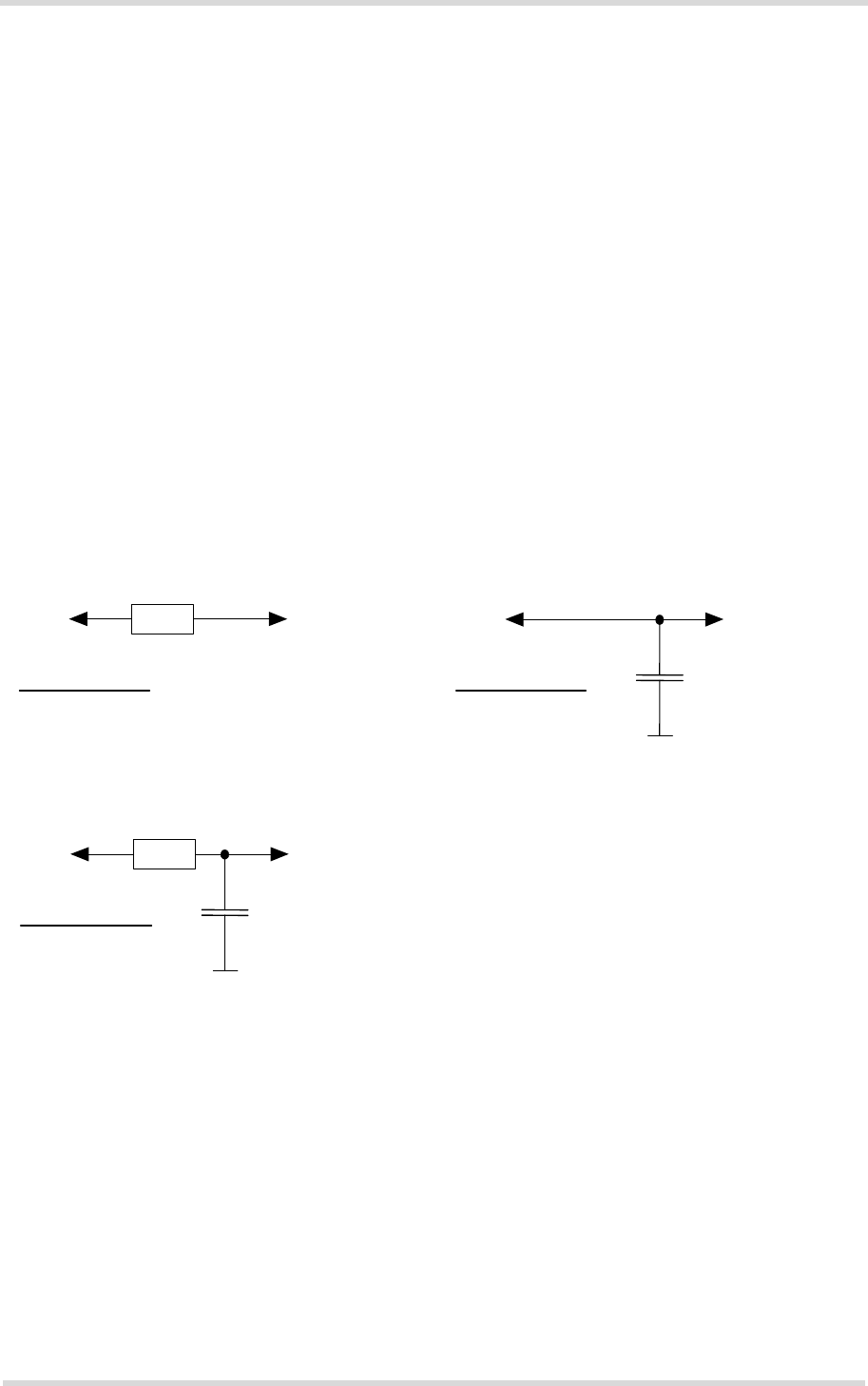
Cinterion® ELS31-VA/ELS51-VA Hardware Interface Description
3.7 Blocking against RF on Interface Lines
76
ELS31-VA_ELS51-VA_HID_v01.000 2017-01-04
Confidential / Preliminary
Page 73 of 106
3.7 Blocking against RF on Interface Lines
To reduce EMI issues there are serial resistors, or capacitors to GND, implemented on the
module for the ignition, emergency restart, and SIM interface lines (cp. Section 2.3). However,
all other signal lines have no EMI measures on the module and there are no blocking measures
at the module’s interface to an external application.
Dependent on the specific application design, it might be useful to implement further EMI mea-
sures on some signal lines at the interface between module and application. These measures
are described below.
There are five possible variants of EMI measures (A-C) that may be implemented between
module and external application depending on the signal line (see Figure 39 and Table 21). Pay
attention not to exceed the maximum input voltages and prevent voltage overshots if using in-
ductive EMC measures.
The maximum value of the serial resistor should be lower than 1k on the signal line. The max-
imum value of the capacitor should be lower than 50pF on the signal line. Please observe the
electrical specification of the module‘s SMT application interface and the external application‘s
interface.
Figure 39: EMI circuits
Note: In case the application uses an internal antenna that is implemented close to the ELS31-
VA/ELS51-VA / ELS51-VA module, Gemalto strongly recommends sufficient EMI measures,
e.g. of type B or C, for each digital input or output.
C
GND
SMT
R
Application
EMI measures A
SMT
R
Application
EMI measures C
C
GND
SMT Application
EMI measures B
Cinterion® ELS31-VA/ELS51-VA Hardware Interface Description
3.7 Blocking against RF on Interface Lines
76
ELS31-VA_ELS51-VA_HID_v01.000 2017-01-04
Confidential / Preliminary
Page 74 of 106
The following table lists EMI measures that may be implemented for each signal line at the
module‘s SMT application interface.
Table 21: EMI measures on the application interface
Signal name EMI measures Remark
ABC
CCIN x
CCRST xxxThe external capacitor should be not higher than
10pF. The value of the capacitor depends on the
external application.
CCIO x x x
CCCLK x x x
RXD0 x x x
TXD0 xxx
CTS0 xxx
RTS0 xxx
GPIO1/DTR0 x x x
GPIO2/DCD0 x x x
GPIO3/DSR0 x x x
GPIO4/FST_SHDN x x x
GPO5/LED x x x
GPIO6 xxx
GPIO7 xxx
GPIO8/COUNTER x x x
GPIO16/RXD1/AP_WAKEUP x x x
GPIO17/TXD1/HOST_ACTIVE x x x
GPIO18/RTS1/CP_WAKEUP x x x
GPIO19/CTS1/SUSPEND x x x
GPIO20/PCM_I2S_OUT x x x
GPIO21/PCM_I2S_IN x x x
GPIO22/PCM_I2S_FSC x x x
GPO23/PCM_I2S_CLK x x x
GPIO24/RING0 x x x
GPIO25 xxx
GPO26/SPI_CS1 x x x
GPIO27/SPI_CS2 x x x
I2CDAT x The rising signal edge is reduced with an addi-
tional capacitor.
I2CCLK x
V180 x
VCORE x
Cinterion® ELS31-VA/ELS51-VA Hardware Interface Description
3.7 Blocking against RF on Interface Lines
76
ELS31-VA_ELS51-VA_HID_v01.000 2017-01-04
Confidential / Preliminary
Page 75 of 106
BATT_RF x Measures required if BATT+RF is close to internal
LTE antenna -
e.g., 39pF blocking capacitor to ground
BATT_BB x
SDIOCMD xxx
SDIOCLK xxx
SDIO0 xxx
SDIO1 xxx
SDIO2 xxx
SDIO3 xxx
HSIC_DATA xxx
HSIC_STRB xxx
Table 21: EMI measures on the application interface
Signal name EMI measures Remark
ABC

Cinterion® ELS31-VA/ELS51-VA Hardware Interface Description
3.8 Reliability Characteristics
76
ELS31-VA_ELS51-VA_HID_v01.000 2017-01-04
Confidential / Preliminary
Page 76 of 106
3.8 Reliability Characteristics
The test conditions stated below are an extract of the complete test specifications.
Table 22: Summary of reliability test conditions
Type of test Conditions Standard
Vibration Frequency range: 10-20Hz; acceleration: 5g
Frequency range: 20-500Hz; acceleration: 20g
Duration: 2h per axis; 3 axes
DIN IEC 60068-2-61
1. For reliability tests in the frequency range 20-500Hz the Standard’s acceleration reference value was
increased to 20g.
Shock half-sinus Acceleration: 500g
Shock duration: 1ms
1 shock per axis
6 positions (± x, y and z)
DIN IEC 60068-2-27
Dry heat Temperature: +70 ±2°C
Test duration: 16h
Humidity in the test chamber: < 50%
EN 60068-2-2 Bb
ETS 300 019-2-7
Temperature
change (shock)
Low temperature: -40°C ±2°C
High temperature: +85°C ±2°C
Changeover time: < 30s (dual chamber system)
Test duration: 1h
Number of repetitions: 100
DIN IEC 60068-2-14 Na
ETS 300 019-2-7
Damp heat cyclic High temperature: +55°C ±2°C
Low temperature: +25°C ±2°C
Humidity: 93% ±3%
Number of repetitions: 6
Test duration: 12h + 12h
DIN IEC 60068-2-30 Db
ETS 300 019-2-5
Cold (constant
exposure)
Temperature: -40 ±2°C
Test duration: 16h
DIN IEC 60068-2-1
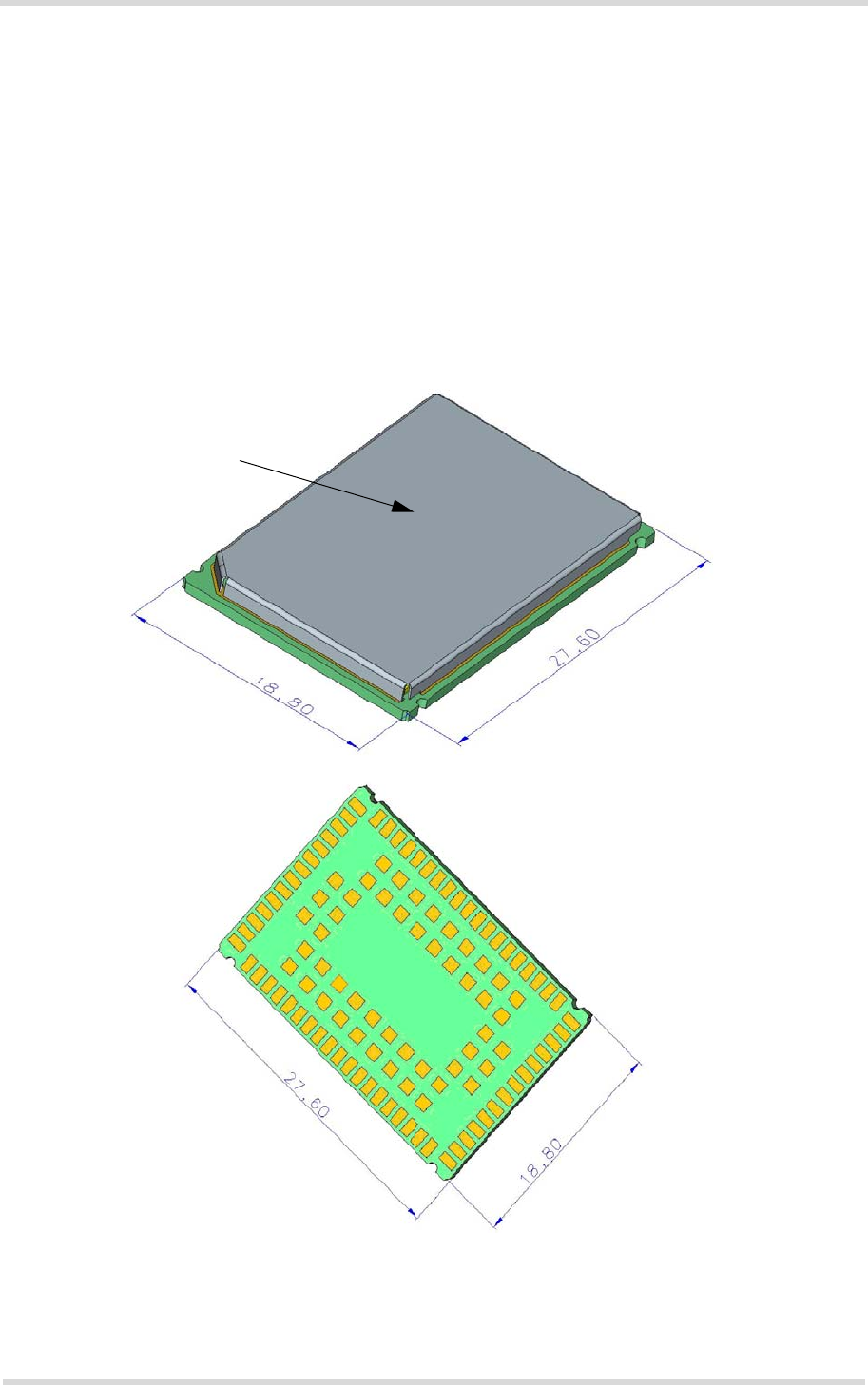
Cinterion® ELS31-VA/ELS51-VA Hardware Interface Description
4 Mechanical Dimensions, Mounting and Packaging
92
ELS31-VA_ELS51-VA_HID_v01.000 2017-01-04
Confidential / Preliminary
Page 77 of 106
4 Mechanical Dimensions, Mounting and Packaging
The following sections describe the mechanical dimensions of ELS31-VA/ELS51-VA and give
recommendations for integrating ELS31-VA/ELS51-VA into the host application.
4.1 Mechanical Dimensions of ELS31-VA/ELS51-VA
Figure 40 shows the top and bottom view of ELS31-VA/ELS51-VA and provides an overview
of the board's mechanical dimensions. For further details see Figure 41.
Figure 40: ELS31-VA/ELS51-VA– top and bottom view
Product label
Top view
Bottom view
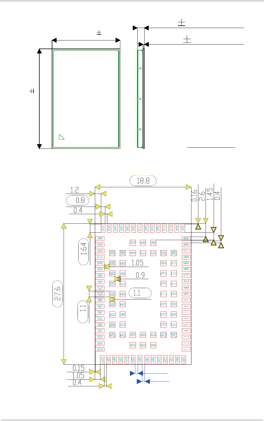
Cinterion® ELS31-VA/ELS51-VA Hardware Interface Description
4.1 Mechanical Dimensions of ELS31-VA/ELS51-VA
92
ELS31-VA_ELS51-VA_HID_v01.000 2017-01-04
Confidential / Preliminary
Page 78 of 106
Figure 41: Dimensions of ELS31-VA/ELS51-VA (all dimensions in mm)
Figure 42: Dimensions of ELS31-VA/ELS51-VA (all dimensions in mm) - bottom view
0.1
18.8
0.1
27.6
0.31 0.04(PCB)
2.05 0.1(TOTAL)
TOP VIEW
18.8
27.6
0.8
1.2
0.4
0.55
0.55
1.05
0.4
2.6
0.4
1.45
1.05
0.15
1.64
0.9
1.1
1.1
0.16
#0550.7*&8
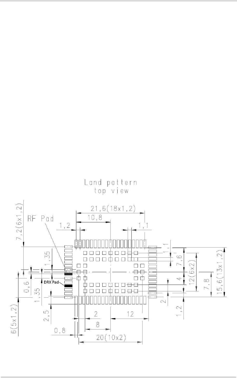
Cinterion® ELS31-VA/ELS51-VA Hardware Interface Description
4.2 Mounting ELS31-VA/ELS51-VA onto the Application Platform
92
ELS31-VA_ELS51-VA_HID_v01.000 2017-01-04
Confidential / Preliminary
Page 79 of 106
4.2 Mounting ELS31-VA/ELS51-VA onto the Application Plat-
form
This section describes how to mount ELS31-VA/ELS51-VA onto the PCBs (=printed circuit
boards), including land pattern and stencil design, board-level characterization, soldering con-
ditions, durability and mechanical handling. For more information on issues related to SMT
module integration see also [4].
Note: To avoid short circuits between signal tracks on an external application's PCB and vari-
ous markings at the bottom side of the module, it is recommended not to route the signal tracks
on the top layer of an external PCB directly under the module, or at least to ensure that signal
track routes are sufficiently covered with solder resist.
4.2.1 SMT PCB Assembly
4.2.1.1 Land Pattern and Stencil
The land pattern and stencil design as shown below is based on Gemalto characterizations for
lead-free solder paste on a four-layer test PCB and a 120 micron thick stencil.
The land pattern given in Figure 43 reflects the module‘s pad layout, including signal pads and
ground pads (for pad assignment see Section 2.1.1).
Figure 43: Land pattern (top view)
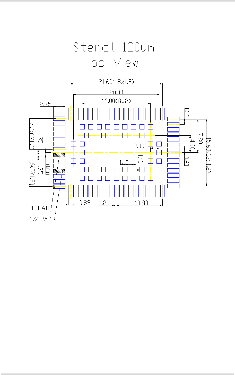
Cinterion® ELS31-VA/ELS51-VA Hardware Interface Description
4.2 Mounting ELS31-VA/ELS51-VA onto the Application Platform
92
ELS31-VA_ELS51-VA_HID_v01.000 2017-01-04
Confidential / Preliminary
Page 80 of 106
The stencil design illustrated in Figure 44 is recommended by Gemalto M2M as a result of ex-
tensive tests with Gemalto M2M Daisy Chain modules.
Figure 44: Recommended design for 120 micron thick stencil (top view, dual design)

Cinterion® ELS31-VA/ELS51-VA Hardware Interface Description
4.2 Mounting ELS31-VA/ELS51-VA onto the Application Platform
92
ELS31-VA_ELS51-VA_HID_v01.000 2017-01-04
Confidential / Preliminary
Page 81 of 106
4.2.1.2 Board Level Characterization
Board level characterization issues should also be taken into account if devising an SMT pro-
cess.
Characterization tests should attempt to optimize the SMT process with regard to board level
reliability. This can be done by performing the following physical tests on sample boards: Peel
test, bend test, tensile pull test, drop shock test and temperature cycling. Sample surface
mount checks are described in [4].
It is recommended to characterize land patterns before an actual PCB production, taking indi-
vidual processes, materials, equipment, stencil design, and reflow profile into account. For land
and stencil pattern design recommendations see also Section 4.2.1.1. Optimizing the solder
stencil pattern design and print process is necessary to ensure print uniformity, to decrease sol-
der voids, and to increase board level reliability.
Daisy chain modules for SMT characterization are available on request. For details refer to [4].
Generally, solder paste manufacturer recommendations for screen printing process parame-
ters and reflow profile conditions should be followed. Maximum ratings are described in Section
4.2.3.
4.2.2 Moisture Sensitivity Level
ELS31-VA/ELS51-VA comprises components that are susceptible to damage induced by ab-
sorbed moisture.
Gemalto M2M’s ELS31-VA/ELS51-VA module complies with the latest revision of the IPC/JE-
DEC J-STD-020 Standard for moisture sensitive surface mount devices and is classified as
MSL 4.
For additional MSL (=moisture sensitivity level) related information see Section 4.2.4 and Sec-
tion 4.3.2.
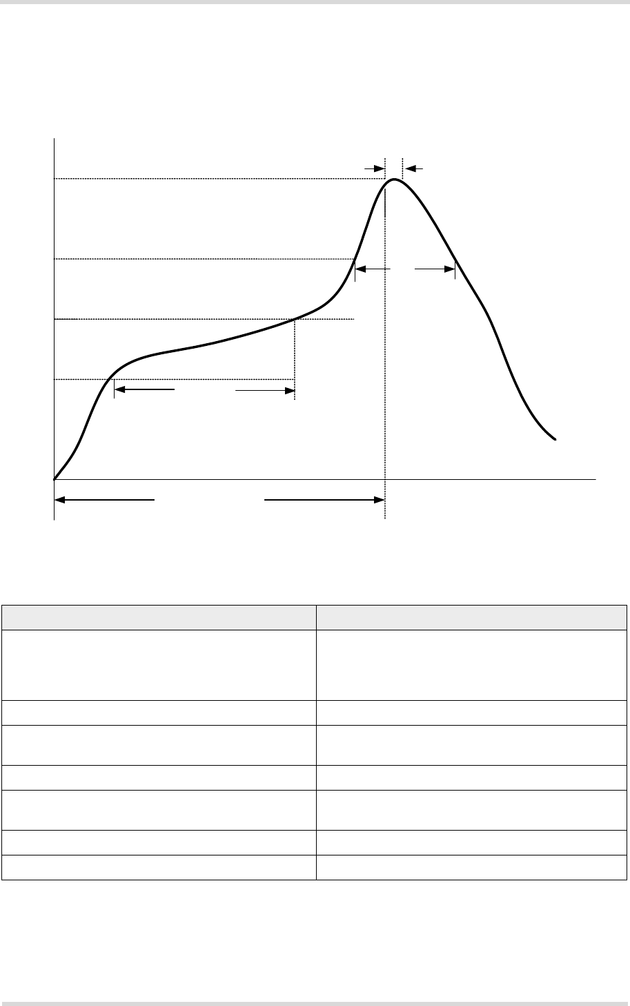
Cinterion® ELS31-VA/ELS51-VA Hardware Interface Description
4.2 Mounting ELS31-VA/ELS51-VA onto the Application Platform
92
ELS31-VA_ELS51-VA_HID_v01.000 2017-01-04
Confidential / Preliminary
Page 82 of 106
4.2.3 Soldering Conditions and Temperature
4.2.3.1 Reflow Profile
Figure 45: Reflow Profile
Table 23: Reflow temperature ratings1
1. Please note that the reflow profile features and ratings listed above are based on the joint industry stan-
dard IPC/JEDEC J-STD-020D.1, and are as such meant as a general guideline. For more information
on reflow profiles and their optimization please refer to [4].
Profile Feature Pb-Free Assembly
Preheat & Soak
Temperature Minimum (TSmin)
Temperature Maximum (TSmax)
Time (tSmin to tSmax) (tS)
150°C
200°C
60-120 seconds
Average ramp up rate (TSmax to TP) 3K/second max.
Liquidous temperature (TL)
Time at liquidous (tL)
217°C
60-90 seconds
Peak package body temperature (TP) 245°C +0/-10°C
Time (tP) within 5 °C of the peak package body
temperature (TP)
20 seconds max.
Average ramp-down rate (TP to TSmax) 3 K/second max.
Time 25°C to maximum temperature 6 minutes max.
TL
TP
tP
tL
tS
Preheat
t to maximum Time
Temperature
TSmin
TSmax

Cinterion® ELS31-VA/ELS51-VA Hardware Interface Description
4.2 Mounting ELS31-VA/ELS51-VA onto the Application Platform
92
ELS31-VA_ELS51-VA_HID_v01.000 2017-01-04
Confidential / Preliminary
Page 83 of 106
4.2.3.2 Maximum Temperature and Duration
The following limits are recommended for the SMT board-level soldering process to attach the
module:
• A maximum module temperature of 240°C. This specifies the temperature as measured at
the module’s top side.
• A maximum duration of 15 seconds at this temperature.
Please note that while the solder paste manufacturers' recommendations for best temperature
and duration for solder reflow should generally be followed, the limits listed above must not be
exceeded.
ELS31-VA/ELS51-VA is specified for one soldering cycle only. Once ELS31-VA/ELS51-VA is
removed from the application, the module will very likely be destroyed and cannot be soldered
onto another application.

Cinterion® ELS31-VA/ELS51-VA Hardware Interface Description
4.2 Mounting ELS31-VA/ELS51-VA onto the Application Platform
92
ELS31-VA_ELS51-VA_HID_v01.000 2017-01-04
Confidential / Preliminary
Page 84 of 106
4.2.4 Durability and Mechanical Handling
4.2.4.1 Storage Conditions
ELS31-VA/ELS51-VA modules, as delivered in tape and reel carriers, must be stored in sealed,
moisture barrier anti-static bags. The conditions stated below are only valid for modules in their
original packed state in weather protected, non-temperature-controlled storage locations. Nor-
mal storage time under these conditions is 12 months maximum.
Table 24: Storage conditions
Type Condition Unit Reference
Air temperature: Low
High
-25
+40
°C IPC/JEDEC J-STD-033A
Humidity relative: Low
High
10
90 at 40°C
%
IPC/JEDEC J-STD-033A
Air pressure: Low
High
70
106
kPa IEC TR 60271-3-1: 1K4
IEC TR 60271-3-1: 1K4
Movement of surrounding air 1.0 m/s IEC TR 60271-3-1: 1K4
Water: rain, dripping, icing and
frosting
Not allowed --- ---
Radiation: Solar
Heat
1120
600
W/m2ETS 300 019-2-1: T1.2, IEC 60068-2-2 Bb
ETS 300 019-2-1: T1.2, IEC 60068-2-2 Bb
Chemically active substances Not
recommended
IEC TR 60271-3-1: 1C1L
Mechanically active substances Not
recommended
IEC TR 60271-3-1: 1S1
Vibration sinusoidal:
Displacement
Acceleration
Frequency range
1.5
5
2-9 9-200
mm
m/s2
Hz
IEC TR 60271-3-1: 1M2
Shocks:
Shock spectrum
Duration
Acceleration
Semi-sinusoidal
1
50
ms
m/s2
IEC 60068-2-27 Ea

Cinterion® ELS31-VA/ELS51-VA Hardware Interface Description
4.2 Mounting ELS31-VA/ELS51-VA onto the Application Platform
92
ELS31-VA_ELS51-VA_HID_v01.000 2017-01-04
Confidential / Preliminary
Page 85 of 106
4.2.4.2 Processing Life
ELS31-VA/ELS51-VA must be soldered to an application within 72 hours after opening the
MBB (=moisture barrier bag) it was stored in.
As specified in the IPC/JEDEC J-STD-033 Standard, the manufacturing site processing the
modules should have ambient temperatures below 30°C and a relative humidity below 60%.
4.2.4.3 Baking
Baking conditions are specified on the moisture sensitivity label attached to each MBB (see
Figure 50 for details):
• It is not necessary to bake ELS31-VA/ELS51-VA, if the conditions specified in Section
4.2.4.1 and Section 4.2.4.2 were not exceeded.
• It is necessary to bake ELS31-VA/ELS51-VA, if any condition specified in Section 4.2.4.1
and Section 4.2.4.2 was exceeded.
If baking is necessary, the modules must be put into trays that can be baked to at least 125°C.
Devices should not be baked in tape and reel carriers at any temperature.
4.2.4.4 Electrostatic Discharge
ESD (=electrostatic discharge) may lead to irreversable damage for the module. It is therefore
advisable to develop measures and methods to counter ESD and to use these to control the
electrostatic environment at manufacturing sites.
Please refer to Section 3.6 for further information on electrostatic discharge.
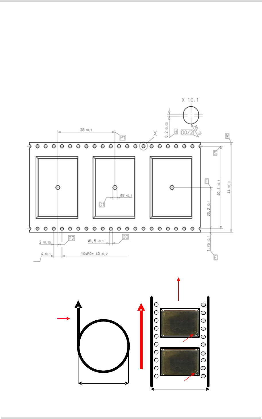
Cinterion® ELS31-VA/ELS51-VA Hardware Interface Description
4.3 Packaging
92
ELS31-VA_ELS51-VA_HID_v01.000 2017-01-04
Confidential / Preliminary
Page 86 of 106
4.3 Packaging
4.3.1 Tape and Reel
The single-feed tape carrier for ELS31-VA/ELS51-VA is illustrated in Figure 46. The figure also
shows the proper part orientation. The tape width is 44 mm and the ELS31-VA/ELS51-VA mod-
ules are placed on the tape with a 28-mm pitch. The reels are 330 mm in diameter with a core
diameter of 100 mm. Each reel contains 500 modules.
4.3.1.1 Orientation
Figure 46: Carrier tape
Figure 47: Reel direction
44 mm
330 mm
Reel direction of the
completely equipped tape Direction into
SMD machine
View
direction
Pad 1
Pad 1
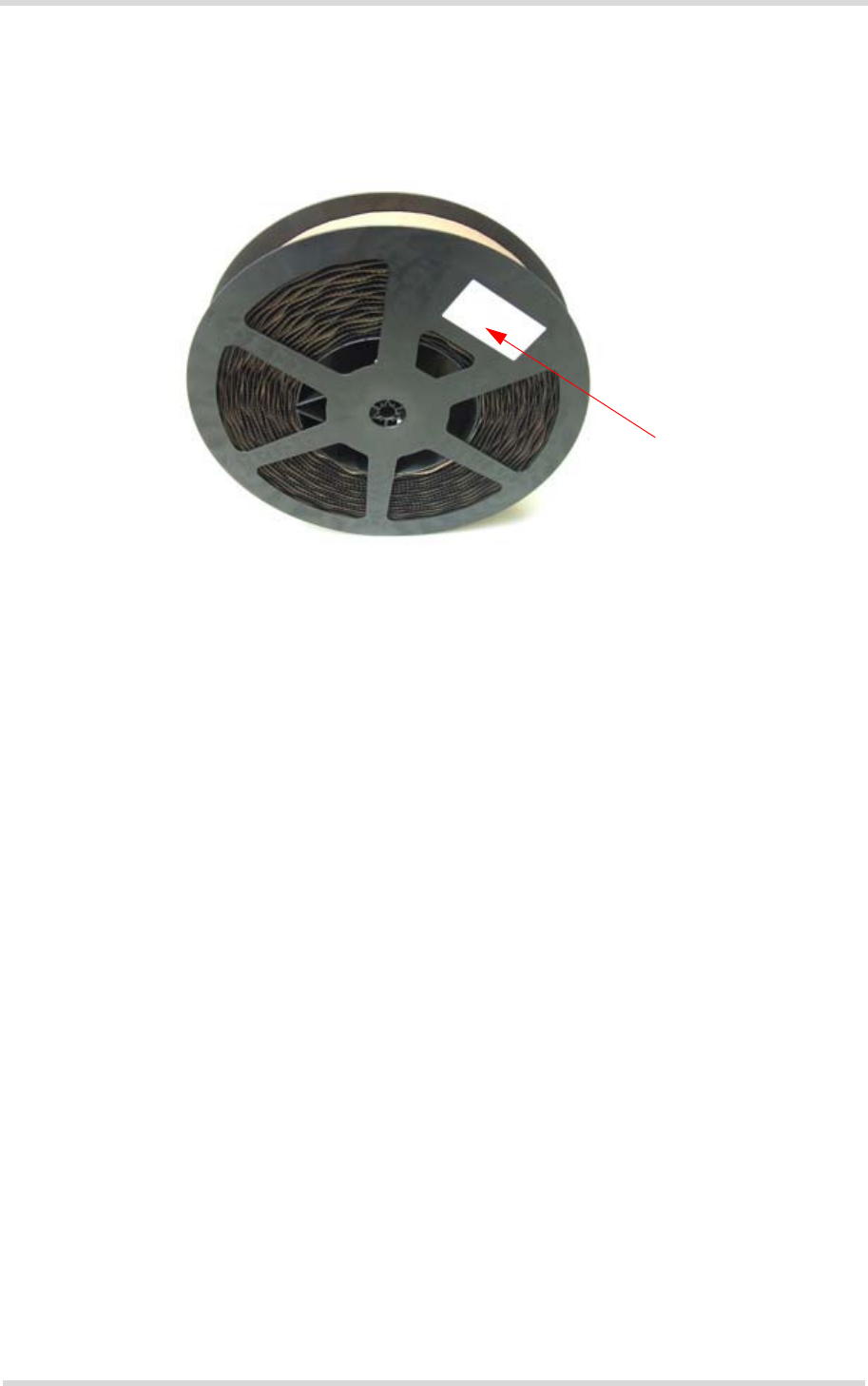
Cinterion® ELS31-VA/ELS51-VA Hardware Interface Description
4.3 Packaging
92
ELS31-VA_ELS51-VA_HID_v01.000 2017-01-04
Confidential / Preliminary
Page 87 of 106
4.3.1.2 Barcode Label
A barcode label provides detailed information on the tape and its contents. It is attached to the
reel.
Figure 48: Barcode label on tape reel
Barcode label
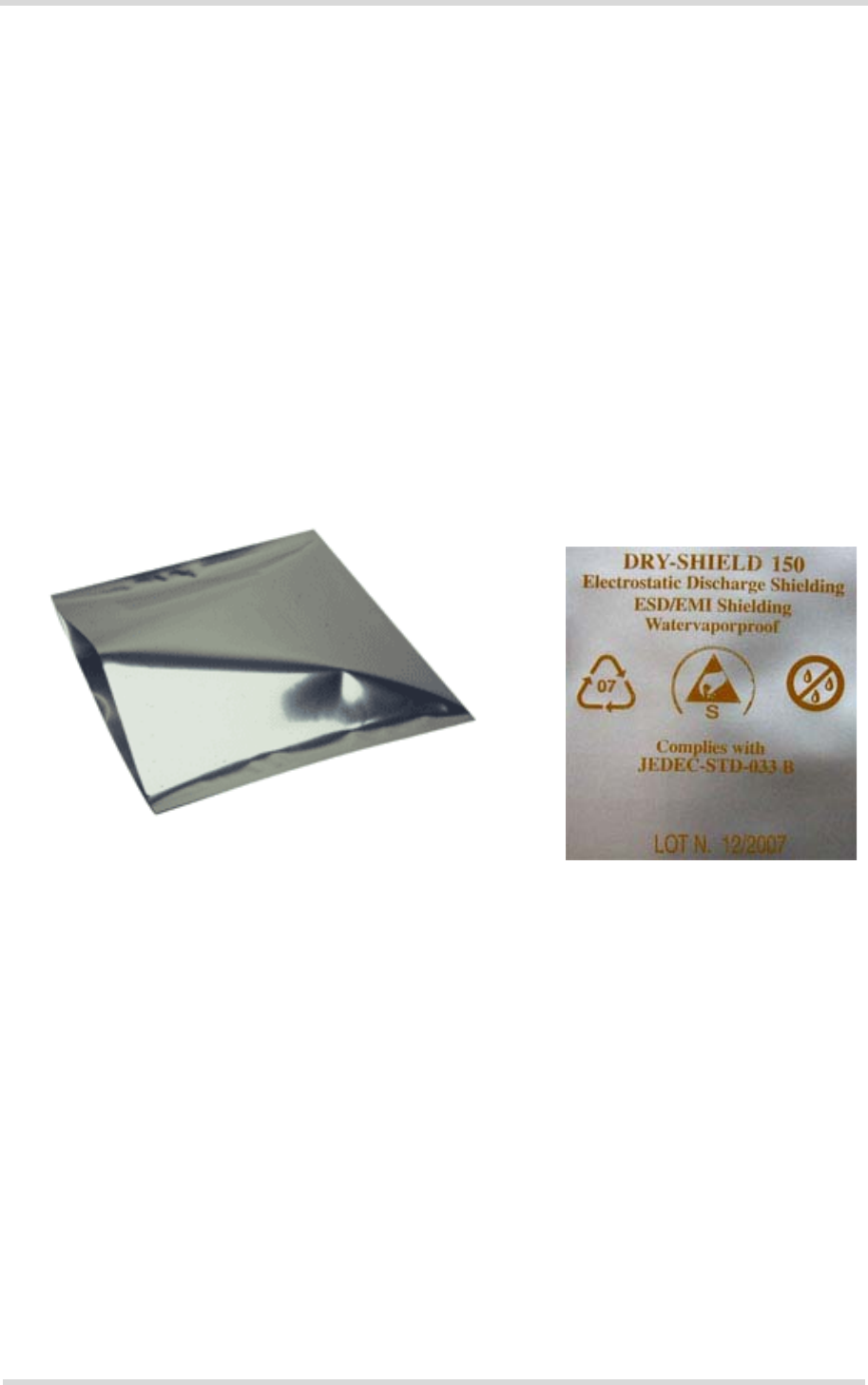
Cinterion® ELS31-VA/ELS51-VA Hardware Interface Description
4.3 Packaging
92
ELS31-VA_ELS51-VA_HID_v01.000 2017-01-04
Confidential / Preliminary
Page 88 of 106
4.3.2 Shipping Materials
ELS31-VA/ELS51-VA is distributed in tape and reel carriers. The tape and reel carriers used
to distribute ELS31-VA/ELS51-VA are packed as described below, including the following re-
quired shipping materials:
• Moisture barrier bag, including desiccant and humidity indicator card
• Transportation box
4.3.2.1 Moisture Barrier Bag
The tape reels are stored inside an MBB (=moisture barrier bag), together with a humidity indi-
cator card and desiccant pouches - see Figure 49. The bag is ESD protected and delimits mois-
ture transmission. It is vacuum-sealed and should be handled carefully to avoid puncturing or
tearing. The bag protects the ELS31-VA/ELS51-VA modules from moisture exposure. It should
not be opened until the devices are ready to be soldered onto the application.
Figure 49: Moisture barrier bag (MBB) with imprint
The label shown in Figure 50 summarizes requirements regarding moisture sensitivity, includ-
ing shelf life and baking requirements. It is attached to the outside of the moisture barrier bag.
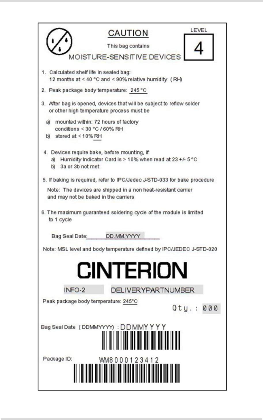
Cinterion® ELS31-VA/ELS51-VA Hardware Interface Description
4.3 Packaging
92
ELS31-VA_ELS51-VA_HID_v01.000 2017-01-04
Confidential / Preliminary
Page 89 of 106
Figure 50: Moisture Sensitivity Label
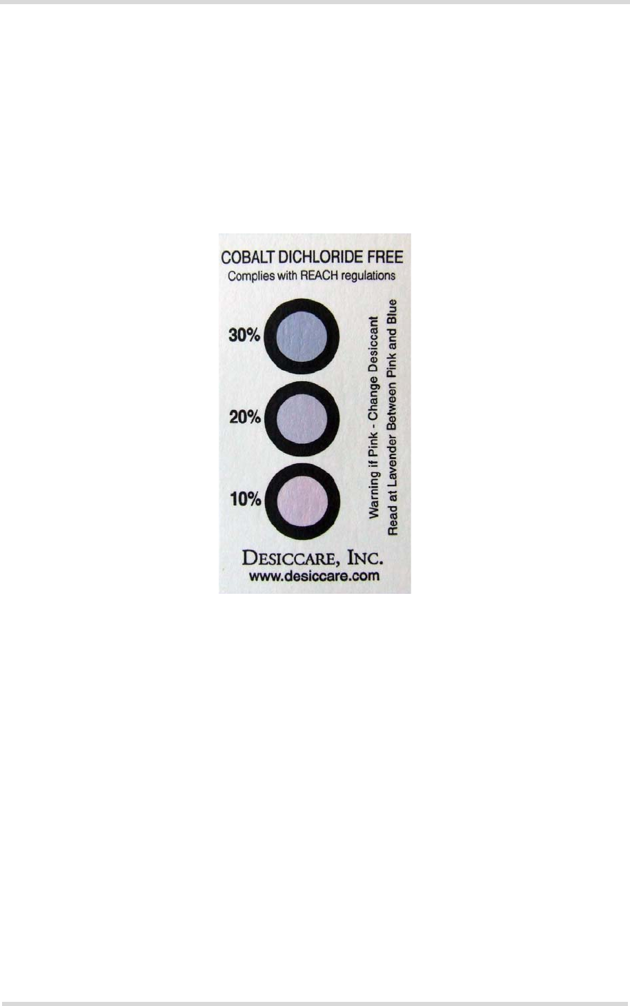
Cinterion® ELS31-VA/ELS51-VA Hardware Interface Description
4.3 Packaging
92
ELS31-VA_ELS51-VA_HID_v01.000 2017-01-04
Confidential / Preliminary
Page 90 of 106
MBBs contain one or more desiccant pouches to absorb moisture that may be in the bag. The
humidity indicator card described below should be used to determine whether the enclosed
components have absorbed an excessive amount of moisture.
The desiccant pouches should not be baked or reused once removed from the MBB.
The humidity indicator card is a moisture indicator and is included in the MBB to show the ap-
proximate relative humidity level within the bag. Sample humidity cards are shown in Figure 51.
If the components have been exposed to moisture above the recommended limits, the units will
have to be rebaked.
Figure 51: Humidity Indicator Card - HIC
A baking is required if the humidity indicator inside the bag indicates 10% RH or more.
4.3.2.2 Transportation Box
Tape and reel carriers are distributed in a box, marked with a barcode label for identification
purposes. A box contains two reels with 500 modules each.
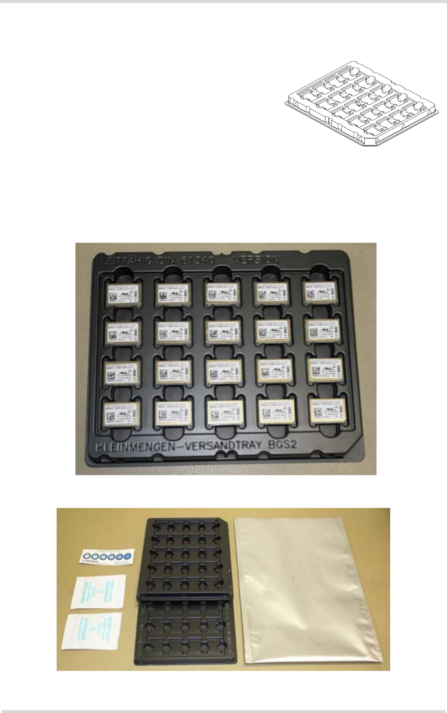
Cinterion® ELS31-VA/ELS51-VA Hardware Interface Description
4.3 Packaging
92
ELS31-VA_ELS51-VA_HID_v01.000 2017-01-04
Confidential / Preliminary
Page 91 of 106
4.3.3 Trays
If small module quantities are required, e.g., for test and
evaluation purposes, ELS31-VA/ELS51-VA may be dis-
tributed in trays (for dimensions see Figure 55). The
small quantity trays are an alternative to the single-feed
tape carriers normally used. However, the trays are not
designed for machine processing. They contain modules
to be (hand) soldered onto an external application (for in-
formation on hand soldering see [4]).
Figure 52: Small quantity tray
Trays are packed and shipped in the same way as tape carriers, including a moisture barrier
bag with desiccant and humidity indicator card as well as a transportation box (see also Section
4.3.2).
Figure 53: Tray to ship odd module amounts
Figure 54: Trays with packaging materials
1:1,5
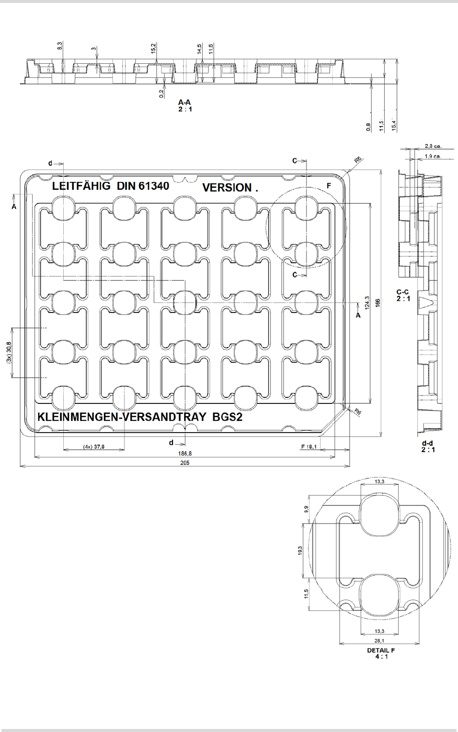
Cinterion® ELS31-VA/ELS51-VA Hardware Interface Description
4.3 Packaging
92
ELS31-VA_ELS51-VA_HID_v01.000 2017-01-04
Confidential / Preliminary
Page 92 of 106
Figure 55: Tray dimensions
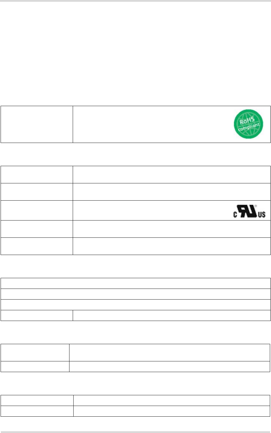
Cinterion® ELS31-VA/ELS51-VA Hardware Interface Description
5 Regulatory and Type Approval Information
98
ELS31-VA_ELS51-VA_HID_v01.000 2017-01-04
Confidential / Preliminary
Page 93 of 106
5 Regulatory and Type Approval Information
5.1 Directives and Standards
ELS31-VA/ELS51-VA is designed to comply with the directives and standards listed below.
It is the responsibility of the application manufacturer to ensure compliance of the final product
with all provisions of the applicable directives and standards as well as with the technical spec-
ifications provided in the "ELS31-VA/ELS51-VA Hardware Interface Description".
Table 25: Directives
2002/95/EC (RoHS 1)
2011/65/EC (RoHS 2)
Directive of the European Parliament and of the Council
of 27 January 2003 (and revised on 8 June 2011) on the
restriction of the use of certain hazardous substances in
electrical and electronic equipment (RoHS)
Table 26: Standards of North American type approval
CFR Title 47 Code of Federal Regulations, Part 22 and Part 24 (Telecommunications,
PCS); US Equipment Authorization FCC
OET Bulletin 65
(Edition 97-01)
Evaluating Compliance with FCC Guidelines for Human Exposure to
Radiofrequency Electromagnetic Fields
UL 60 950-1 Product Safety Certification (Safety requirements)
California Leadfree Man-
date
Covered by European RoHS requirements
RSS132 (Issue2)
RSS133 (Issue5)
Canadian Standard
Table 27: Standards of Verizon type approval
Verizon Wireless Unified Module Process for Compliance Testing and Approval, October 2014
Verizon Wireless Device Requirements LTE 3GPP Band 13 Network Access, October 2014
Verizon Wireless Device Requirements LTE 3GPP Band 4 Network Access, October 2014
3GPP2 C.S0015-A v1.0 Short Message Service for spread spectrum systems
Table 28: Standards of GCF type approval
3GPP TS 51.010-1 Digital cellular telecommunications system (Release 10); Mobile Station
(MS) conformance specification;
GCF-CC V3.58 Global Certification Forum - Certification Criteria
Table 29: Requirements of quality
IEC 60068 Environmental testing
DIN EN 60529 IP codes
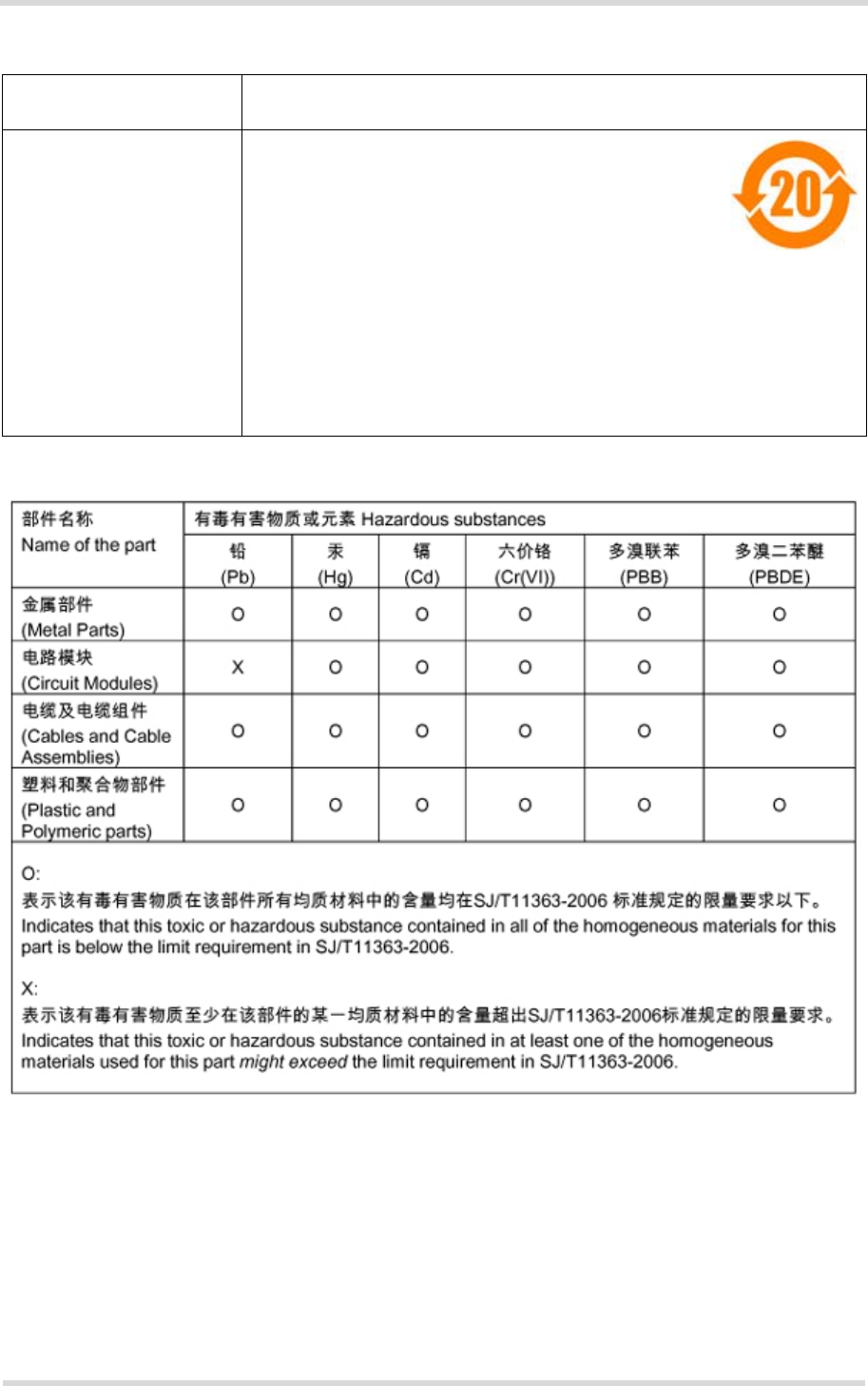
Cinterion® ELS31-VA/ELS51-VA Hardware Interface Description
5.1 Directives and Standards
98
ELS31-VA_ELS51-VA_HID_v01.000 2017-01-04
Confidential / Preliminary
Page 94 of 106
Table 31: Toxic or hazardous substances or elements with defined concentration limits
Table 30: Standards of the Ministry of Information Industry of the People’s Republic of China
SJ/T 11363-2006 “Requirements for Concentration Limits for Certain Hazardous Sub-
stances in Electronic Information Products” (2006-06).
SJ/T 11364-2006 “Marking for Control of Pollution Caused by Electronic
Information Products” (2006-06).
According to the “Chinese Administration on the Control
of Pollution caused by Electronic Information Products”
(ACPEIP) the EPUP, i.e., Environmental Protection Use
Period, of this product is 20 years as per the symbol
shown here, unless otherwise marked. The EPUP is valid only as long as
the product is operated within the operating limits described in the
Gemalto M2M Hardware Interface Description.
Please see Table 31 for an overview of toxic or hazardous substances or
elements that might be contained in product parts in concentrations
above the limits defined by SJ/T 11363-2006.

Cinterion® ELS31-VA/ELS51-VA Hardware Interface Description
5.2 SAR requirements specific to portable mobiles
98
ELS31-VA_ELS51-VA_HID_v01.000 2017-01-04
Confidential / Preliminary
Page 95 of 106
5.2 SAR requirements specific to portable mobiles
Mobile phones, PDAs or other portable transmitters and receivers incorporating a GSM module
must be in accordance with the guidelines for human exposure to radio frequency energy. This
requires the Specific Absorption Rate (SAR) of portable ELS31-VA/ELS51-VA based applica-
tions to be evaluated and approved for compliance with national and/or international regula-
tions.
Since the SAR value varies significantly with the individual product design manufacturers are
advised to submit their product for approval if designed for portable use. For US markets the
relevant directives are mentioned below. It is the responsibility of the manufacturer of the final
product to verify whether or not further standards, recommendations or directives are in force
outside these areas.
Products intended for sale on US markets
ES 59005/ANSI C95.1 Considerations for evaluation of human exposure to Electromagnetic
Fields (EMFs) from Mobile Telecommunication Equipment (MTE) in the
frequency range 30MHz - 6GHz
Please note that SAR requirements are specific only for portable devices and not for mobile
devices as defined below:
• Portable device:
A portable device is defined as a transmitting device designed to be used so that the radi-
ating structure(s) of the device is/are within 20 centimeters of the body of the user.
• Mobile device:
A mobile device is defined as a transmitting device designed to be used in other than fixed
locations and to generally be used in such a way that a separation distance of at least 20
centimeters is normally maintained between the transmitter's radiating structure(s) and the
body of the user or nearby persons. In this context, the term ''fixed location'' means that the
device is physically secured at one location and is not able to be easily moved to another
location.
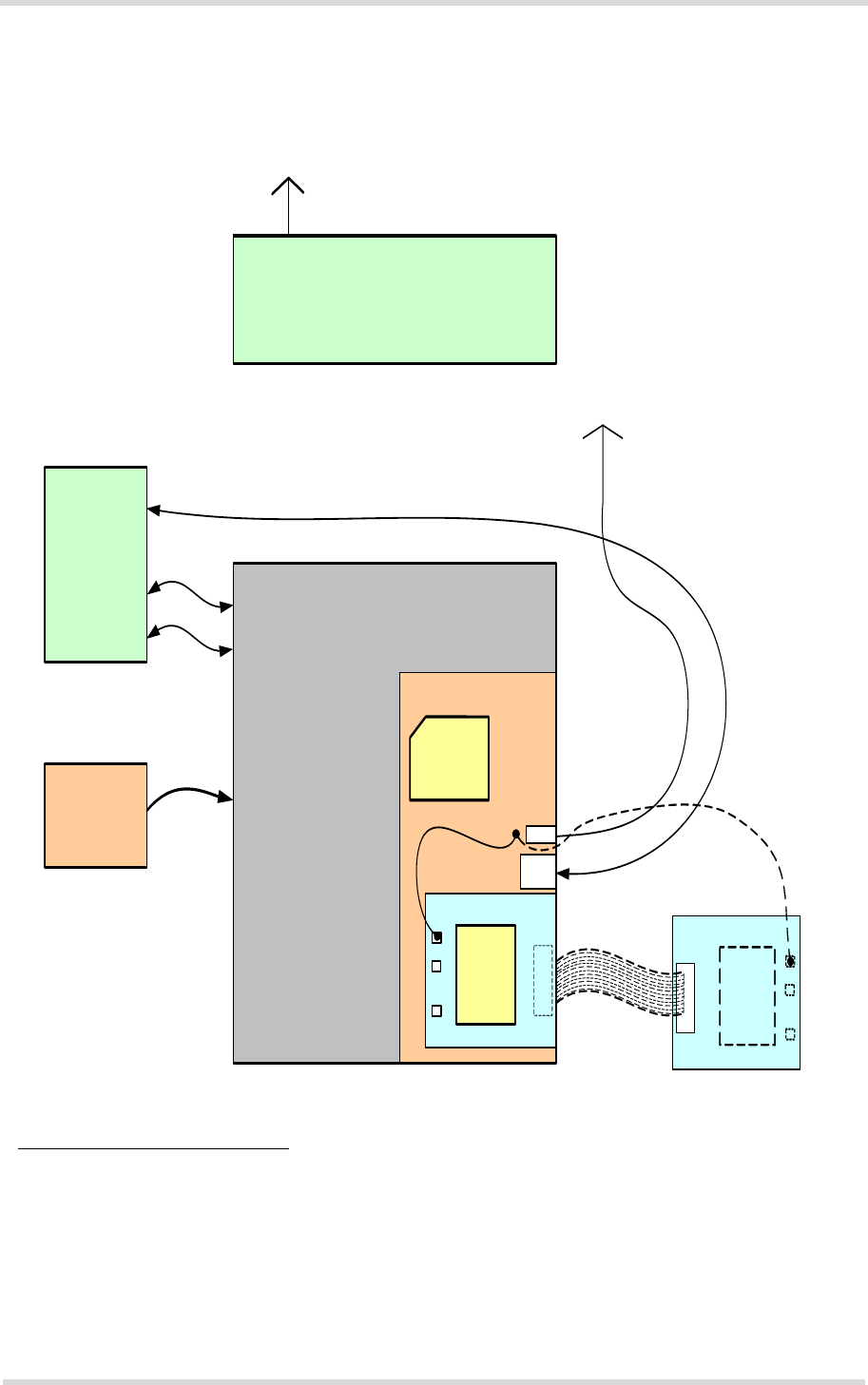
Cinterion® ELS31-VA/ELS51-VA Hardware Interface Description
5.3 Reference Equipment for Type Approval
98
ELS31-VA_ELS51-VA_HID_v01.000 2017-01-04
Confidential / Preliminary
Page 96 of 106
5.3 Reference Equipment for Type Approval
The Gemalto M2M reference setup submitted to type approve ELS31-VA/ELS51-VA (including
a special approval adapter for the DSB75) is shown in the following figure1:
Figure 56: Reference equipment for Type Approval
1. For RF performance tests a mini-SMT/U.FL to SMA adapter with attached 6dB coaxial attenuator is cho-
sen to connect the evaluation module directly to the GSM/UMTS test equipment instead of employing
the SMA antenna connectors on the ELS31-VA/ELS51-VA-DSB75 adapter as shown in Figure 56. The
following products are recommended:
Hirose SMA-Jack/U.FL-Plug conversion adapter HRMJ-U.FLP(40)
(for details see see http://www.hirose-connectors.com/ or http://www.farnell.com/
Aeroflex Weinschel Fixed Coaxial Attenuator Model 3T/4T
(for details see http://www.aeroflex.com/ams/weinschel/pdfiles/wmod3&4T.pdf)
Antenna
GSM / GPRS / UMTS
Antenna with 1m cable
ASC0
PC
Power
supply
LTE
Base station
DSB75
ASC1
USB
Approval adapter for
DSB75
SMA
Evaluation module
ELS31
ELS51
USB
Evaluation module
ELS31
ELS51
SIM card
Top view
Bottom view
Cinterion® ELS31-VA/ELS51-VA Hardware Interface Description
5.4 Compliance with FCC and IC Rules and Regulations
98
ELS31-VA_ELS51-VA_HID_v01.000 2017-01-04
Confidential / Preliminary
Page 97 of 106
5.4 Compliance with FCC and IC Rules and Regulations
The Equipment Authorization Certification for the Gemalto M2M reference application de-
scribed in Section 5.3 will be registered under the following identifiers:
• ELS31-VA:
FCC Identifier: QIPELS31-VA
Industry Canada Certification Number: 7830A-ELS31VA
Granted to Gemalto M2M GmbH
• ELS51-VA:
FCC Identifier: QIPELS51-VA (not yet granted)
Industry Canada Certification Number: 7830A-ELS51VA (not yet granted)
Granted to Gemalto M2M GmbH
Manufacturers of mobile or fixed devices incorporating ELS31-VA/ELS51-VA modules are au-
thorized to use the FCC Grants and Industry Canada Certificates of the ELS31-VA/ELS51-VA
modules for their own final products according to the conditions referenced in these docu-
ments. In this case, an FCC/ IC label of the module shall be visible from the outside, or the host
device shall bear a second label stating "Contains FCC ID: QIPELS31-VA" / "Contains FCC ID:
QIPELS51-VA", and accordingly “Contains IC: 7830A-ELS31VA“ / “Contains IC: 7830A-ELS51-
VA“. The integration is limited to fixed or mobile categorized host devices, where a separation
distance between the antenna and any person of min. 20cm can be assured during normal op-
erating conditions.
For mobile and fixed operation configurations the antenna gain, including cable loss, must not
exceed the limits in the following Table 28 for FCC and IC.
IMPORTANT:
Manufacturers of portable applications incorporating ELS31-VA/ELS51-VA modules are re-
quired to have their final product certified and apply for their own FCC Grant and Industry Can-
ada Certificate related to the specific portable mobile. This is mandatory to meet the SAR
requirements for portable mobiles (see Section 5.2 for detail).
Changes or modifications not expressly approved by the party responsible for compliance
could void the user's authority to operate the equipment.
Note: This equipment has been tested and found to comply with the limits for a Class B digital
device, pursuant to part 15 of the FCC Rules and with Industry Canada license-exempt RSS
standard(s). These limits are designed to provide reasonable protection against harmful inter-
ference in a residential installation. This equipment generates, uses and can radiate radio fre-
quency energy and, if not installed and used in accordance with the instructions, may cause
harmful interference to radio communications. However, there is no guarantee that interference
Table 32: Antenna gain limits for FCC and IC
Operating band FCC limit IC limit Unit
Maximum gain in lower operating bands with f< 1GHz
(LTE Bd13)
10.4 7.4 dBi
Maximum gain in higher operating bands with f=1700MHz
(LTE Bd4)
6.5 6.5 dBi

Cinterion® ELS31-VA/ELS51-VA Hardware Interface Description
5.4 Compliance with FCC and IC Rules and Regulations
98
ELS31-VA_ELS51-VA_HID_v01.000 2017-01-04
Confidential / Preliminary
Page 98 of 106
will not occur in a particular installation. If this equipment does cause harmful interference to
radio or television reception, which can be determined by turning the equipment off and on, the
user is encouraged to try to correct the interference by one or more of the following measures:
• Reorient or relocate the receiving antenna.
• Increase the separation between the equipment and receiver.
• Connect the equipment into an outlet on a circuit different from that to which the receiver is
connected.
• Consult the dealer or an experienced radio/TV technician for help.
This Class B digital apparatus complies with Canadian ICES-003.
If Canadian approval is requested for devices incorporating ELS31VA / ELS51-VA modules the
above note will have to be provided in the English and French language in the final user docu-
mentation. Manufacturers/OEM Integrators must ensure that the final user documentation does
not contain any information on how to install or remove the module from the final product.
Notes (IC):
(EN) This Class B digital apparatus complies with Canadian ICES-003 and RSS-210. Opera-
tion is subject to the following two conditions: (1) this device may not cause interference, and
(2) this device must accept any interference, including interference that may cause undesired
operation of the device.
(FR) Cet appareil numérique de classe B est conforme aux normes canadiennes ICES-003 et
RSS-210. Son fonctionnement est soumis aux deux conditions suivantes: (1) cet appareil ne
doit pas causer d'interférence et (2) cet appareil doit accepter toute interférence, notamment
les interférences qui peuvent affecter son fonctionnement.
(EN) Radio frequency (RF) Exposure Information
The radiated output power of the Wireless Device is below the Industry Canada (IC) radio fre-
quency exposure limits. The Wireless Device should be used in such a manner such that the
potential for human contact during normal operation is minimized.
This device has also been evaluated and shown compliant with the IC RF Exposure limits un-
der mobile exposure conditions (antennas at least 20cm from a person‘s body).
(FR) Informations concernant l'exposltion aux fréquences radio (RF)
La puissance de sortie émise par l'appareil de sans fiI est inférieure à la limite d'exposition aux
fréquences radio d‘Industry Canada (IC). Utilisez l'appareil de sans fil de façon à minimiser les
contacts humains lors du fonctionnement normal.
Ce périphérique a également été évalué et démontré conforme aux limites d'exposition aux RF
d'IC dans des conditions d'exposition à des appareils mobiles (les antennes se situent à moins
de 20cm du corps d'une personne).

Cinterion® ELS31-VA/ELS51-VA Hardware Interface Description
6 Document Information
103
ELS31-VA_ELS51-VA_HID_v01.000 2017-01-04
Confidential / Preliminary
Page 99 of 106
6 Document Information
6.1 Revision History
New document: "Cinterion® ELS31-VA/ELS51-VA Hardware Interface Description" v01.000
Chapter What is new
-- Initial document setup.

Cinterion® ELS31-VA/ELS51-VA Hardware Interface Description
6.2 Related Documents
103
ELS31-VA_ELS51-VA_HID_v01.000 2017-01-04
Confidential / Preliminary
Page 100 of 106
6.2 Related Documents
[1] ELS31-VA/ELS51-VA AT Command Set
[2] ELS31-VA/ELS51-VA Release Note
[3] Application Note 40: Thermal Solutions
[4] Application Note 48: SMT Module Integration
[5] Universal Serial Bus Specification Revision 2.0, April 27, 2000
6.3 Terms and Abbreviations
Abbreviation Description
ADC Analog-to-digital converter
AGC Automatic Gain Control
ANSI American National Standards Institute
ARFCN Absolute Radio Frequency Channel Number
ARP Antenna Reference Point
ASC0/ASC1 Asynchronous Controller. Abbreviations used for first and second serial interface of
the module
B Thermistor Constant
BER Bit Error Rate
BTS Base Transceiver Station
CB or CBM Cell Broadcast Message
CE Conformité Européene (European Conformity)
CHAP Challenge Handshake Authentication Protocol
CPU Central Processing Unit
CS Coding Scheme
CSD Circuit Switched Data
CTS Clear to Send
DAC Digital-to-Analog Converter
DAI Digital Audio Interface
dBm0 Digital level, 3.14dBm0 corresponds to full scale, see ITU G.711, A-law
DCE Data Communication Equipment (typically modems, e.g. Gemalto M2M module)
DCS 1800 Digital Cellular System, also referred to as PCN
DRX Discontinuous Reception
DSB Development Support Box
DSP Digital Signal Processor
DSR Data Set Ready
DTE Data Terminal Equipment (typically computer, terminal, printer or, for example, GSM
application)

Cinterion® ELS31-VA/ELS51-VA Hardware Interface Description
6.3 Terms and Abbreviations
103
ELS31-VA_ELS51-VA_HID_v01.000 2017-01-04
Confidential / Preliminary
Page 101 of 106
DTR Data Terminal Ready
DTX Discontinuous Transmission
EFR Enhanced Full Rate
EGSM Enhanced GSM
EIRP Equivalent Isotropic Radiated Power
EMC Electromagnetic Compatibility
ERP Effective Radiated Power
ESD Electrostatic Discharge
ETS European Telecommunication Standard
FCC Federal Communications Commission (U.S.)
FDMA Frequency Division Multiple Access
FR Full Rate
GMSK Gaussian Minimum Shift Keying
GPIO General Purpose Input/Output
GPRS General Packet Radio Service
GSM Global Standard for Mobile Communications
HiZ High Impedance
HR Half Rate
HSIC High-Speed Inter-Chip
I/O Input/Output
IC Integrated Circuit
IMEI International Mobile Equipment Identity
ISO International Standards Organization
ITU International Telecommunications Union
kbps kbits per second
LED Light Emitting Diode
Li-Ion/Li+ Lithium-Ion
Li battery Rechargeable Lithium Ion or Lithium Polymer battery
LTE Long Term Evolution
Mbps Mbits per second
MMI Man Machine Interface
MO Mobile Originated
MS Mobile Station (GSM module), also referred to as TE
MSISDN Mobile Station International ISDN number
MT Mobile Terminated
NTC Negative Temperature Coefficient
OEM Original Equipment Manufacturer
Abbreviation Description

Cinterion® ELS31-VA/ELS51-VA Hardware Interface Description
6.3 Terms and Abbreviations
103
ELS31-VA_ELS51-VA_HID_v01.000 2017-01-04
Confidential / Preliminary
Page 102 of 106
PA Power Amplifier
PAP Password Authentication Protocol
PBCCH Packet Switched Broadcast Control Channel
PCB Printed Circuit Board
PCL Power Control Level
PCM Pulse Code Modulation
PCN Personal Communications Network, also referred to as DCS 1800
PCS Personal Communication System, also referred to as GSM 1900
PLL Phase Locked Loop
PPP Point-to-point protocol
PSK Phase Shift Keying
PSU Power Supply Unit
R&TTE Radio and Telecommunication Terminal Equipment
RAM Random Access Memory
RF Radio Frequency
RLS Radio Link Stability
RoHS Restriction of the use of certain hazardous substances in electrical and electronic
equipment.
RTS Request to Send
Rx Receive Direction
SAR Specific Absorption Rate
SAW Surface Acoustic Wave
SDIO Secure Digital Input Output
SELV Safety Extra Low Voltage
SIM Subscriber Identification Module
SMD Surface Mount Device
SMS Short Message Service
SMT Surface Mount Technology
SRAM Static Random Access Memory
TA Terminal adapter (e.g. GSM module)
TDMA Time Division Multiple Access
TE Terminal Equipment, also referred to as DTE
TLS Transport Layer Security
Tx Transmit Direction
UART Universal asynchronous receiver-transmitter
URC Unsolicited Result Code
USSD Unstructured Supplementary Service Data
VSWR Voltage Standing Wave Ratio
Abbreviation Description
Cinterion® ELS31-VA/ELS51-VA Hardware Interface Description
6.4 Safety Precaution Notes
103
ELS31-VA_ELS51-VA_HID_v01.000 2017-01-04
Confidential / Preliminary
Page 103 of 106
6.4 Safety Precaution Notes
The following safety precautions must be observed during all phases of the operation, usage,
service or repair of any cellular terminal or mobile incorporating ELS31-VA/ELS51-VA. Manu-
facturers of the cellular terminal are advised to convey the following safety information to users
and operating personnel and to incorporate these guidelines into all manuals supplied with the
product. Failure to comply with these precautions violates safety standards of design, manu-
facture and intended use of the product. Gemalto M2M assumes no liability for customer’s fail-
ure to comply with these precautions.
When in a hospital or other health care facility, observe the restrictions on the use of
mobiles. Switch the cellular terminal or mobile off, if instructed to do so by the guide-
lines posted in sensitive areas. Medical equipment may be sensitive to RF energy.
The operation of cardiac pacemakers, other implanted medical equipment and hear-
ing aids can be affected by interference from cellular terminals or mobiles placed close
to the device. If in doubt about potential danger, contact the physician or the manufac-
turer of the device to verify that the equipment is properly shielded. Pacemaker
patients are advised to keep their hand-held mobile away from the pacemaker, while
it is on.
Switch off the cellular terminal or mobile before boarding an aircraft. Make sure it can-
not be switched on inadvertently. The operation of wireless appliances in an aircraft is
forbidden to prevent interference with communications systems. Failure to observe
these instructions may lead to the suspension or denial of cellular services to the
offender, legal action, or both.
Do not operate the cellular terminal or mobile in the presence of flammable gases or
fumes. Switch off the cellular terminal when you are near petrol stations, fuel depots,
chemical plants or where blasting operations are in progress. Operation of any elec-
trical equipment in potentially explosive atmospheres can constitute a safety hazard.
Your cellular terminal or mobile receives and transmits radio frequency energy while
switched on. Remember that interference can occur if it is used close to TV sets,
radios, computers or inadequately shielded equipment. Follow any special regulations
and always switch off the cellular terminal or mobile wherever forbidden, or when you
suspect that it may cause interference or danger.
Road safety comes first! Do not use a hand-held cellular terminal or mobile when driv-
ing a vehicle, unless it is securely mounted in a holder for speakerphone operation.
Before making a call with a hand-held terminal or mobile, park the vehicle.
Speakerphones must be installed by qualified personnel. Faulty installation or opera-
tion can constitute a safety hazard.
IMPORTANT!
Cellular terminals or mobiles operate using radio signals and cellular networks.
Because of this, connection cannot be guaranteed at all times under all conditions.
Therefore, you should never rely solely upon any wireless device for essential com-
munications, for example emergency calls.
Remember, in order to make or receive calls, the cellular terminal or mobile must be
switched on and in a service area with adequate cellular signal strength.
Some networks do not allow for emergency calls if certain network services or phone
features are in use (e.g. lock functions, fixed dialing etc.). You may need to deactivate
those features before you can make an emergency call.
Some networks require that a valid SIM card be properly inserted in the cellular termi-
nal or mobile.

Cinterion® ELS31-VA/ELS51-VA Hardware Interface Description
7 Appendix
105
ELS31-VA_ELS51-VA_HID_v01.000 2017-01-04
Confidential / Preliminary
Page 104 of 106
7 Appendix
7.1 List of Parts and Accessories
Table 33: List of parts and accessories
Description Supplier Ordering information
ELS31-VA Gemalto M2M Standard module
Gemalto M2M IMEI:
Packaging unit (ordering) number:
L30960-N4580-A300
Module label number:
L30960-N4580-A300-11
1. Note: At the discretion of Gemalto M2M, module label information can either be laser engraved on the
module’s shielding or be printed on a label adhered to the module’s shielding.
ELS51-VA Gemalto M2M Standard module
Gemalto M2M IMEI:
Packaging unit (ordering) number:
L30960-N4590-A300
Module label number:
L30960-N4590-A300-11
ELS31-VA Evaluation Mod-
ule
Gemalto M2M Ordering number:
L30960-N4581-A300
ELS51-VA Evaluation Mod-
ule
Gemalto M2M Ordering number:
L30960-N4591-A300
DSB75 Evaluation Kit Gemalto M2M Ordering number: L36880-N8811-A100
DSB Mini
Compact Evaluation Board
Gemalto M2M Ordering number: L30960-N0030-A100
Starter Kit B80 Gemalto M2M Ordering Number L30960-N0040-A100
Multi-Adapter R1 for mount-
ing ELS31-VA/ELS51-VA
evaluation modules onto
DSB75
Gemalto M2M Ordering number: L30960-N0010-A100
Approval adapter for mount-
ing ELS31-VA/ELS51-VA
evaluation modules onto
DSB75
Gemalto M2M Ordering number: L30960-N2301-A100
SIM card holder incl. push
button ejector and slide-in
tray
Molex Ordering numbers: 91228
91236
Sales contacts are listed in Table 34.

Cinterion® ELS31-VA/ELS51-VA Hardware Interface Description
7.1 List of Parts and Accessories
105
ELS31-VA_ELS51-VA_HID_v01.000 2017-01-04
Confidential / Preliminary
Page 105 of 106
Table 34: Molex sales contacts (subject to change)
Molex
For further information please click:
http://www.molex.com
Molex Deutschland GmbH
Otto-Hahn-Str. 1b
69190 Walldorf
Germany
Phone: +49-6227-3091-0
Fax: +49-6227-3091-8100
Email: mxgermany@molex.com
American Headquarters
Lisle, Illinois 60532
U.S.A.
Phone: +1-800-78MOLEX
Fax: +1-630-969-1352
Molex China Distributors
Beijing,
Room 1311, Tower B, COFCO Plaza
No. 8, Jian Guo Men Nei Street, 100005
Beijing
P.R. China
Phone: +86-10-6526-9628
Fax: +86-10-6526-9730
Molex Singapore Pte. Ltd.
110, International Road
Jurong Town,
Singapore 629174
Phone: +65-6-268-6868
Fax: +65-6-265-6044
Molex Japan Co. Ltd.
1-5-4 Fukami-Higashi,
Yamato-City,
Kanagawa, 242-8585
Japan
Phone: +81-46-265-2325
Fax: +81-46-265-2365

106
M2M.GEMALTO.COM
About Gemalto
Gemalto (Euronext NL0000400653 GTO) is the world leader in digital security with 2015 annual
revenues of €3.1 billion and blue-chip customers in over 180 countries. Our 14,000+ employees
operate out of 118 offices, 45 personalization and data centers, and 27 research and software
development centers located in 49 countries.
We are at the heart of the rapidly evolving digital society. Billions of people worldwide increasingly
want the freedom to communicate, travel, shop, bank, entertain and work - anytime, everywhere
- in ways that are enjoyable and safe. Gemalto delivers on their expanding needs for personal
mobile services, payment security, authenticated cloud access, identity and privacy protection,
eHealthcare and eGovernment efficiency, convenient ticketing and dependable machine-to-
machine (M2M) applications.
Gemalto develops secure embedded software and secure products which we design and
personalize. Our platforms and services manage these secure products, the confidential data they
contain and the trusted end-user services they enable. Our innovations enable our clients to offer
trusted and convenient digital services to billions of individuals.
Gemalto thrives with the growing number of people using its solutions to interact with the digital
and wireless world.
For more information please visit
m2m.gemalto.com, www.facebook.com/gemalto, or Follow@gemaltom2m on twitter.
Gemalto M2M GmbH
Werinherstrasse 81
81541 Munich
Germany
© Gemalto 2017. All rights reserved. Gemalto, the Gemalto logo, are trademarks and service marks of Gemalto and are registered in certain countries. April 2013