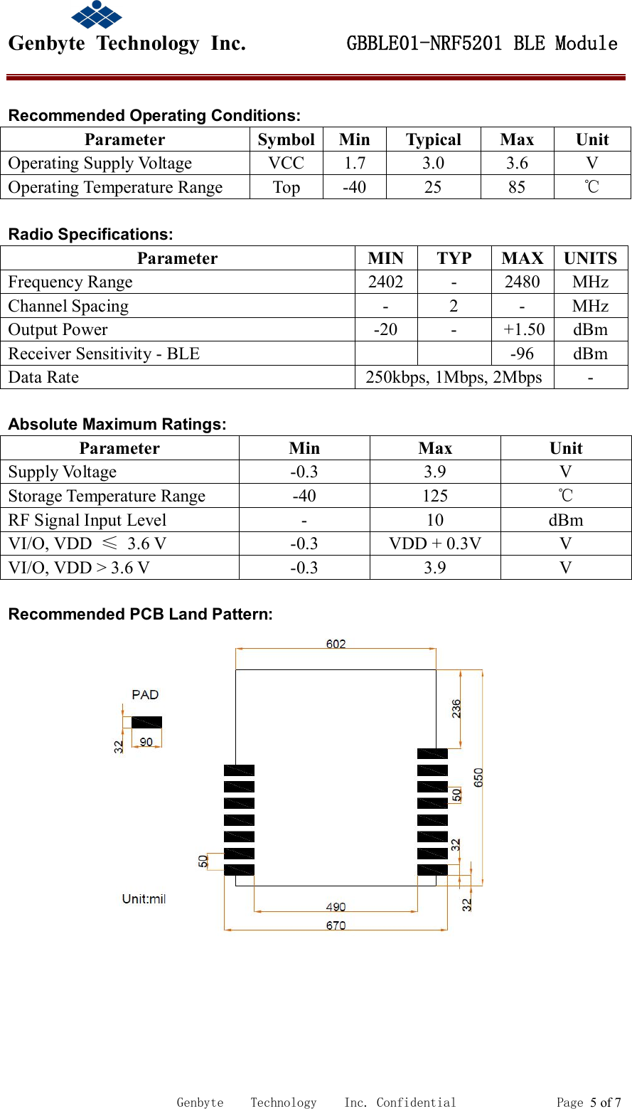
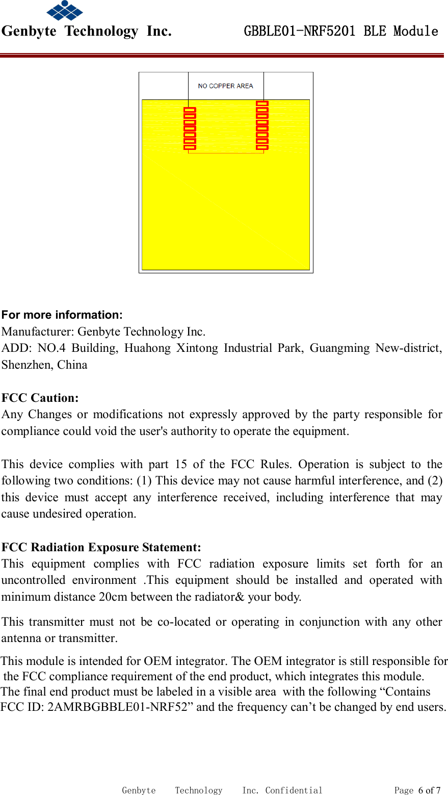
Genbyte Technology GBBLE01-NRF52 BLE Module User Manual

Genbyte Technology Inc. BLE Module

User Manual

                                            Genbyte  Technology  Inc.         GBBLE01-NRF5201 BLE Module                                                             Genbyte    Technology    Inc. Confidential               Page 1 of 7        GBBLE01-NRF5201 BLE Module Instructions         Version:V1.0 Date:Mar, 2018
                                            Genbyte  Technology  Inc.         GBBLE01-NRF5201 BLE Module                                                             Genbyte    Technology    Inc. Confidential               Page 2 of 7 GBBLE01-NRF5201 BLE Module General Description GBBLE01-NRF5201  is  a  powerful,  multiprotocol, ultra  low  power  Bluetooth  Low  Energy  (BLE) module using Nordic nRF52832 SoC. With an ARM Cortex  TM  M4F  MCU,  512KB  flash,  64KB  RAM, embedded  2.4GHz  multi-protocol  transceiver,  and an  integrated  chip  antenna.  It  provide  a  comple solution  with  no  extral  RF  design,  allows  faster time to market with reduced development cost.  Overview and Features  Based on Nordic Semiconductor’s nRF52832 BLE SoC;  Complete RF solution with integrated antenna;  Multi-Protocol 2.4GHz Radio;  32-bit ARM Cortex M4F processor;  Serial Wire Debug (SWD);  Over-the-Air (OTA) firmware update;  Flash/RAM: 512KB/64KB:  11 General purpose I/O pins:  12 bit/200KSPS ADC;  SPI Master/Slave (8Mbps);  Low power comparator;  Two 2-wire Master/Slave (I 2 C compatible);  I2S audio interface;  UART (with CTS/RTS and DMA);  20 channel CPU independent Programmable Peripheral Interconnect (PPI);  Quadrature Demodulator (QDEC);  128-bit AES HW encryption;  5 x 32 bits, 3 x 24 bits Real Time Counters (RTC);  Internal RC Oscillator 32.768kHz;  Receiver Sensitivity: -96 dBm;  TX power: +/- 0dBm; programmable +4dBm to -20dBm in 4 dB steps;  Sizes: 16.5*15.3*2.7mm;  Integrated chip antenna;  Operation voltage: 1.7V to 3.6V;  Operation temperature: -40°C to +85°C;  Application:  IoT Connected Devices, Appliances;  Bluetooth Low Energy Sensors;
                                            Genbyte  Technology  Inc.         GBBLE01-NRF5201 BLE Module                                                             Genbyte    Technology    Inc. Confidential               Page 3 of 7  Wearable;  Beacons/Proximity;  Lighting products;  Home Automation and Control;  Toys and Gaming;  Mechanical Specification:
                                            Genbyte  Technology  Inc.         GBBLE01-NRF5201 BLE Module                                                             Genbyte    Technology    Inc. Confidential               Page 4 of 7 PIN Description: Number Signal Name Signal Description  Note 1  P0.11  I/O   2  P0.12  I/O   3  P0.13  I/O   4  SWDIO  Debug and flash programming I/O  5  SWDCLK  Debug and flash programming I/O  6  P0.17  I/O   7  P0.18  I/O   8  P0.21  Reset/IO  Configurable as reset 9  GND  Power Ground   10  VDD  Power Supply   11  P0.26  I/O   12  P0.27  I/O   13  P0.28  ADC IN   14  P0.29  ADC IN   15  P0.30  ADC IN    GPIO Electrical Specification: The  module  has  up  to  32  GPIOs available.  All  GPIOs can  be  mapped to  a module, facilitating design and enabling changes after the hardware has been configured. Each GPIO is configurable with the following features:  Input/output direction  Output drive strength  Internal pull-up and pull-down resistors  Wake-up from high or low level triggers on all pins  Trigger interrupt on all pins  All pins can be used by the PPI task/event system; the maximum number of pins that can be interfaced through the PPI at the same time is limited by the number of GPIOTE channels  All pins can be individually configured to carry serial interface or quadrature demodulator signals  HW debug and flash programming of Module : The  module  support  the  two  pin  Serial  Wire  Debug  (SWD)  interface  and  offers flexible  and  powerful  mechanism  for  non-intrusive  debugging  of  program  code. Breakpoints, single stepping, and instruction trace capture of code execution flow are part of this support.  Pin  Flash Program interface SWDIO  Debug and flash programming I/O SWCLK  Debug and flash programming I/O
                                            Genbyte  Technology  Inc.         GBBLE01-NRF5201 BLE Module                                                             Genbyte    Technology    Inc. Confidential               Page 5 of 7  Recommended Operating Conditions: Parameter  Symbol  Min  Typical  Max  Unit Operating Supply Voltage  VCC  1.7  3.0  3.6  V Operating Temperature Range  Top  -40  25  85  ℃  Radio Specifications: Parameter MIN TYP MAX UNITS Frequency Range  2402  -  2480  MHz Channel Spacing  -  2  -  MHz Output Power  -20  -  +1.50  dBm Receiver Sensitivity - BLE      -96  dBm Data Rate  250kbps, 1Mbps, 2Mbps  -  Absolute Maximum Ratings: Parameter  Min  Max  Unit Supply Voltage  -0.3  3.9  V Storage Temperature Range  -40  125  ℃ RF Signal Input Level  -  10  dBm VI/O, VDD  ≤  3.6 V  -0.3  VDD + 0.3V  V VI/O, VDD > 3.6 V  -0.3  3.9  V  Recommended PCB Land Pattern:
                                            Genbyte  Technology  Inc.         GBBLE01-NRF5201 BLE Module                                                             Genbyte    Technology    Inc. Confidential               Page 6 of 7   For more information: Manufacturer: Genbyte Technology Inc. ADD:  NO.4  Building,  Huahong  Xintong  Industrial  Park,  Guangming  New-district, Shenzhen, China  FCC Caution: Any  Changes  or  modifications  not  expressly  approved  by  the  party  responsible  for compliance could void the user's authority to operate the equipment.    This  device  complies  with  part  15  of  the  FCC  Rules.  Operation  is  subject  to  the following two conditions: (1) This device may not cause harmful interference, and (2) this  device  must  accept  any  interference  received,  including  interference  that  may cause undesired operation.    FCC Radiation Exposure Statement:     This  equipment  complies  with  FCC  radiation  exposure  limits  set  forth  for  an uncontrolled  environment  .This  equipment  should  be  installed  and  operated  with minimum distance 20cm between the radiator& your body.     This  transmitter  must  not  be  co-located  or  operating  in  conjunction  with  any  other antenna or transmitter.aaannnaaannnttteeennnnnnaaa   ooorrr   tttrrraaannnsssmmmiiitttttteeerrr...   ttt eee nnn nnn aaa     ooo r rr     ttt r rr aaa nnn ss s mmm iii ttt ttt eee r rr ...                        This module is intended for OEM integrator. The OEM integrator is still responsible for                         the FCC compliance requirement of the end product, which integrates this module.                        The final end product must be labeled in a visible area  with the following “Contains                      FCC ID: 2AMRBGBBLE01-NRF52” and the frequency can’t be changed by end users.
                                            Genbyte  Technology  Inc.         GBBLE01-NRF5201 BLE Module                                                             Genbyte    Technology    Inc. Confidential               Page 7 of 7  ATTENTION !         Electrostatic Sensitive Device         Observe Precaution for handing.   Reversion History Rev  Issued by  Checked by  Approved by V1.0  Li Zhang  Leon  Jiaxiang Zeng   Important notice : ●Genbyte  Technology  Inc.  reserve  the  right  to  make  corrections,  enhancements, improvements and other changes to its products. ●Buyer acknowledges and agrees that it is solely responsible for compliance with all legal, regulatory and safety-related requirements concerning its products. ●Reserves the right to correct, modify, and/or improve products and/or specifications without notice.

Navigation menu