General Dynamics Broand PEMAAU2 Wireless Broadband Modem User Manual Integration Guide

General Dynamics Broadband, Inc. Wireless Broadband Modem Integration Guide
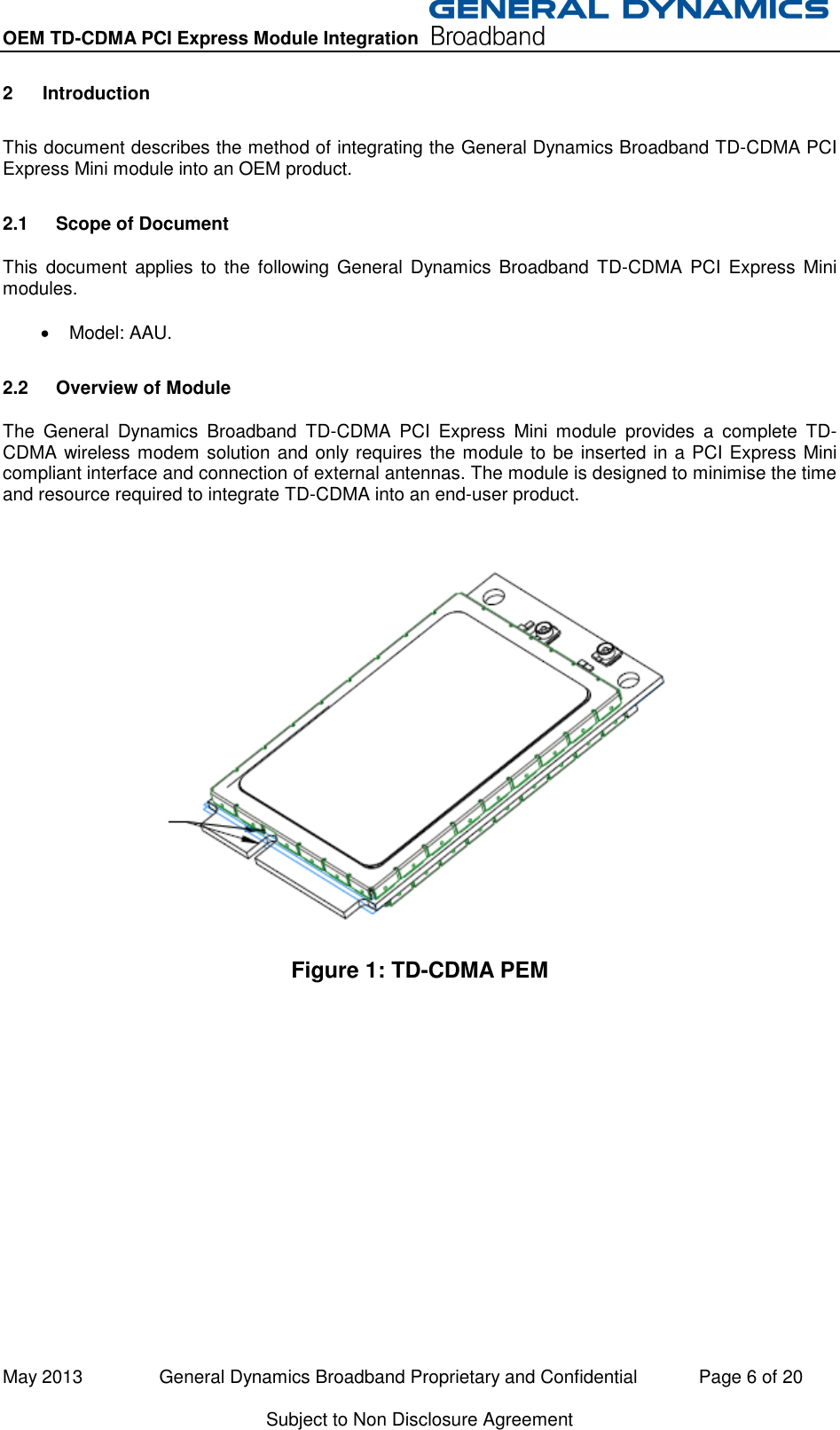
Integration Guide

OEM TD-CDMA PCI Express Module Integration   May 2013               General Dynamics Broadband Proprietary and Confidential            Page 1 of 20 Subject to Non Disclosure Agreement        OEM TD-CDMA PCI Express Mini Module Integration Guide      V01.01
OEM TD-CDMA PCI Express Module Integration   May 2013               General Dynamics Broadband Proprietary and Confidential            Page 2 of 20 Subject to Non Disclosure Agreement Contents 1 General ................................................................................................................ 4 1.1 Approvals and Dates ............................................................................................................... 4 1.2 Change Record ....................................................................................................................... 4 1.3 Acronyms ................................................................................................................................ 5 1.4 External References ................................................................................................................ 5 2 Introduction .......................................................................................................... 6 2.1 Scope of Document ................................................................................................................. 6 2.2 Overview of Module ................................................................................................................. 6 3 Module Connections ............................................................................................ 7 3.1 PCI Express Mini Interface (J1) .............................................................................................. 7 3.1.1 Universal Serial Bus ........................................................................................................ 7 3.1.2 SIM Interface ................................................................................................................... 7 3.1.3 Co-existence Pins ........................................................................................................... 7 3.2 RF Connections ....................................................................................................................... 7 3.3 DC Power ................................................................................................................................ 7 3.4 Management of Radio Receiver Self-Interference .................................................................. 8 3.4.1 PCB Level ........................................................................................................................ 8 3.4.2 Unit Level ......................................................................................................................... 9 3.4.3 Connecting Cables .......................................................................................................... 9 3.4.4 System Level ................................................................................................................... 9 3.4.5 Provision for “Production Modifications” of Host Equipment ......................................... 10 4 Mechanical ........................................................................................................ 11 4.1 Thermal Management ........................................................................................................... 12 4.1.1 PEM Thermal Specification ........................................................................................... 12 4.1.2 PEM and TD-CDMA Adaptor Thermal Specification ..................................................... 13 4.1.3 Physical Thermal Arrangement – PEM and Adaptor ..................................................... 15 4.1.4 PEM and Adaptor Simulated Environment within theoretical enclosure ....................... 16 4.1.5 Recommendations for thermal cooling schemes .......................................................... 17 4.1.6 PEM and Adaptor .......................................................................................................... 17
OEM TD-CDMA PCI Express Module Integration   May 2013               General Dynamics Broadband Proprietary and Confidential            Page 3 of 20 Subject to Non Disclosure Agreement 4.1.7 PEM in Laptop ............................................................................................................... 17 5 Regulatory Information – Model AAU 2.5GHz Band. ......................................... 18 5.1 FCC Requirements for North America .................................................................................. 18 5.1.1 Compliance with FCC Rules and Regulations .............................................................. 18 5.1.2 FCC Labelling Requirements ........................................................................................ 18 5.1.3 Exposure to Radio Frequency Signals .......................................................................... 18 5.1.4 Antenna Gains for Standalone Operation ..................................................................... 19 6 Annex 1: PCI Express Mini Edge Connector Pinout .......................................... 20  Figures Figure 1: TD-CDMA PEM ........................................................................................................................ 6 Figure 2: TD-CDMA PEM RF Connections ............................................................................................. 7 Figure 3: TD-CDMA PEM Module - detail ............................................................................................. 11 Figure 4: PEM Unit Assembly - Top ...................................................................................................... 12 Figure 5: PEM Unit Assembly Bottom ................................................................................................... 13 Figure 6: PEM and Adapter Assembly - Top ......................................................................................... 14 Figure 7: PEM and Adaptor Assembly - Bottom.................................................................................... 14 Figure 8: PEM and Adapter Thermal Assembly Structure Section ....................................................... 16
OEM TD-CDMA PCI Express Module Integration   May 2013               General Dynamics Broadband Proprietary and Confidential            Page 4 of 20 Subject to Non Disclosure Agreement 1  General   1.1  Approvals and Dates  Approval Date W. J. Jones   1.2  Change Record Date Version Author Reason For Change Issue 30/08/2013 01.00 PFW New Document. 30/09/2013 01.01 PFW Updated RF Exposure information
OEM TD-CDMA PCI Express Module Integration   May 2013               General Dynamics Broadband Proprietary and Confidential            Page 5 of 20 Subject to Non Disclosure Agreement 1.3  Acronyms Term Definition TD-CDMA Time Division – Code Division Multiple Access MPE Maximum Permissible Exposure OEM Original Equipment Manufacturer PCIe PCI Express PCI SIG PCI Special Interest Group PEM PCI Express Mini SIM Subscriber Identity Module USB Universal Serial Bus  1.4  External References Ref () Number Title 1 FCC Part 15 Radio Frequency Devices 2 FCC Part 22 Public Mobile Services 3 FCC Part 24 Personal Communication Services 4 FCC Part 27 Miscellaneous Wireless Communications Services 5 FCC Part 90 Private Land Mobile Radio Services 6 PCI SIG PCI Express Base Specification Revision 2.0 7 PCI SIG Card Electromechanical Specification Revision 2.0 8 IPWireless PEM + Adapter Thermal Specification Revision 1.0 Note: Where a reference is undated, the latest version applies unless a specific revision is defined.
OEM TD-CDMA PCI Express Module Integration   May 2013               General Dynamics Broadband Proprietary and Confidential            Page 6 of 20 Subject to Non Disclosure Agreement 2  Introduction This document describes the method of integrating the General Dynamics Broadband TD-CDMA PCI Express Mini module into an OEM product. 2.1  Scope of Document This  document  applies to the  following  General Dynamics Broadband  TD-CDMA  PCI Express  Mini modules.   Model: AAU. 2.2  Overview of Module The  General  Dynamics  Broadband  TD-CDMA  PCI  Express  Mini  module  provides  a  complete  TD-CDMA wireless modem solution and only requires the module to be inserted in a PCI Express Mini compliant interface and connection of external antennas. The module is designed to minimise the time and resource required to integrate TD-CDMA into an end-user product.   Figure 1: TD-CDMA PEM
OEM TD-CDMA PCI Express Module Integration   May 2013               General Dynamics Broadband Proprietary and Confidential            Page 7 of 20 Subject to Non Disclosure Agreement 3  Module Connections 3.1  PCI Express Mini Interface (J1) The General Dynamics Broadband TD-CDMA PCI Express Mini module is provided with a 52 pin edge connector for connection to the external application. This connection supports the following interface types and these are described below. The pinout is shown in Annex 1. 3.1.1  Universal Serial Bus The  PCI  Express  edge  connector  provides  a  USB  2.0  interface,  this  interface  supports  low  speed (1.5Mbps), full speed (12Mbps) and High speed (480Mbps) operation. 3.1.2  SIM Interface The PCI Express edge connector provides a 4 line SIM interface to allow use with Subscriber Identity Modules if  required,  this  interface  supports  both  1.8V  and  3.0V  SIM’s.  The  SIM  interface  does  not provide ESD protection and this should be provided by the host device. 3.1.3 Co-existence Pins The co-existence pins COEX1,2 are currently not supported by the TD-CDMA PEM. 3.2  RF Connections The General Dynamics Broadband TD-CDMA PCI Express Mini module provides two RF connections for  external  antennas.  The  main  port  must  be  connected,  the  diversity  port  may  or  may  not  be connected depending upon application. The connector type is the Hirose U.FL series.   Figure 2: TD-CDMA PEM RF Connections 3.3  DC Power The module requires a DC supply of between 3.0V to 3.6VDC with the nominal voltage being 3.3VDC, maximum input current is 950mA at 3.3VDC (3.1Watts). DC power is applied to the module via the PCI Express Mini edge connector. Diversity Port Main Port
OEM TD-CDMA PCI Express Module Integration   May 2013               General Dynamics Broadband Proprietary and Confidential            Page 8 of 20 Subject to Non Disclosure Agreement 3.4  Management of Radio Receiver Self-Interference The General Dynamics Broadband TD-CDMA PEM is supplied as a stand-alone PCI Express Card, or can be mounted on an General Dynamics Broadband TD-CDMA Adaptor card. It is the customer who then  has  to  integrate  the  PEM  -  either  on  a  Host  Circuit  Board,  or  mounted  within  their  own  Host Equipment,  at  which  point,  the  location  of  the  antennas  which  connect  to  the  PEM  are  outside  of General Dynamics Broadband control. Any radio receiver is susceptible to in-band RF interference in its receive band and it is of paramount importance  that  the  PEM  Host  Equipment  Integration  Design  team  are  aware  of  and  take countermeasures to  prevent  all Host Equipment,  in-band RF  interference from  reaching the  PEM’s Antennas. The PEM as a unit is fully shielded by design, external RF Interference from the Host Equipment is extremely unlikely to get  into the  TD-CDMA Radio receiver  on the PCB  and will be coupled to the receiver by other means. Any Interference from the Host Equipment in the TD-CDMA receive band(s) will  degrade  the  TD-CDMA  receiver  performance  if  present  at  the  antennas.  Any  such  receiver interference is a called an RF “Blocking signal”. The closer the  TD-CDMA PEM’s antenna system is relative  to  the  source  of  any  blocking  signals,  the  worse  will  be  the  degradation  in  Rx  Sensitivity suffered by the TD-CDMA PEM and subsequent customer-perceived Host Equipment performance. Due to the extremely high performance of the TD-CDMA PEM RF Receivers, tiny levels of in-band interference may cause major loss of performance. To put this in perspective, the Class B EMC limit is approximately 70dB higher than the smallest signal that the TD-CDMA Receiver can receive (receiver sensitivity is approximately -123dBm (-16dBµV). Therefore host equipment which is compliant with relevant EMC emission regulations is likely to cause interference and performance degradation to the TD-CDMA PEM receivers. However,  all  of  the  EMC  design  countermeasures  must  be  applied  when  designing  the  Host Equipment, to prevent RF Blocking signals – they are the first line of suppression and are good design practice. Each engineering discipline: Digital, Power, RF, Mechanical and Thermal must be involved from the outset, to provide the suppression performance required. 3.4.1  PCB Level Any PCB with high-clock rate digital signals, imperfect  supply rails and  any signals with fast edges must be carefully designed during layout to produce a low emission profile PCB. By  listing  the  speeds  of  all  clocks,  processors  and  busses,  then  computing  their  harmonics  up  to 2690MHz,  it  is  simple  to  see  which  parts  of  the  circuitry  are  most  likely  to  generate  RF  Blocking signals. Believing that any of those harmonics will destroy RF Receiver performance if they are not suppressed by design and then being meticulous attention during layout are the key to suppressing them at source. a.  Top and bottom surfaces should be flood-filled with a copper ground plane and tracking on the outer layers should be avoided. b.  The perimeter of the PCB should have ground copper on each layer and all layers should be stitched with ground vias. c.  There must be no slots in the surface ground planes or apertures above fast-moving signals on inner layers – particularly digital buses. d.  Care  should  be taken  to provide  ground current  return paths  for all  power  circuitry, for  the digital ICs and particularly the clock ICs. e.  Provision should be made for shielding all components on the PCB.
OEM TD-CDMA PCI Express Module Integration   May 2013               General Dynamics Broadband Proprietary and Confidential            Page 9 of 20 Subject to Non Disclosure Agreement f.  Designers must be aware that PCB connectors contain exposed metal which will radiate and design  and  shield  accordingly.  Provision  should  be  provided  for  options  to  link  connector shields to PCB ground if the best way is not clear, or is not known. 3.4.2  Unit Level The ideal way to suppress RF interferers is to enclose all of the active circuitry in a metal can without holes or joins. Unit level shielding, either SMT or PTH aims go get as close to an ideally shielded metal box as possible within the constraints of reality – i.e. functionality and cost. a.  SMT shielding should be used to cover all components on each side of any PCB that might radiate into the Antenna System. b.  The shielding system should be fully integrated with the PCB surface flood fill ground planes with small distances between connection points. c.  The shielding system should be un-lidded or have many mechanical connection points around the perimeter of the lids used. d.  Special  attention  should  be  paid  to  signals  that  must  travel  outside  of  the  metal  shield  to suppress/filter high speed edges – e.g. R/C filters on LED driving signals. e.  Shielded PCB sockets must be chosen for all interconnect signals and the shield metal must correctly routed and grounded, separate to any circuit ground or power signals carried within the connection bus. f.  Wherever possible, always, filter every interconnect signal, inside the metal shields, with the appropriate filtering components, including the power signals. g.  Whilst instances are much rarer, it should be noted that the UE Transmit signal is capable of inducing false edges onto unshielded digital signals when they are operating in close proximity to antennas carrying pulsed, maximum power Tx signals (notably GSM). 3.4.3  Connecting Cables Choosing the unshielded version of an interconnect but connector system is a false economy if a high sensitivity RF receiver antenna is nearby. Always use the shielded system from the outset and design it in correctly as detailed above. The socket and connector shields are as much part of the shielding as the flood-fill PCB ground planes. a.  If a cable end-connector does not encompass all of the cable cores with a shield then it will radiate. Ensure the connector is fully shielded. b.  If the drain wire/foil/sheath of a shielded cable is not correctly connected to the metal shield within the cable-end connector then it will radiate. c.  If both ends of a shielded cable cannot be shielded (e.g. 100m Ethernet) then ensure that it is at the far end of the cable that the shield is not connected, not the TD-CDMA PEM Antenna end. 3.4.4  System Level Some choices made at the system level can directly affect the Receive performance on the TD-CDMA PEM, as follows. a.  If  possible,  ensure  that  the  main  lobes  of  the  PEM’s  antenna  system  (particularly  if  it  is directional) are not pointing at either the Host Equipment electronics. Assume that all active electronics radiate RF Blockers until proven otherwise. E.g. If the User Equipment is placed in the trunk of a vehicle and the antennas are cabled onto the roof of a car, that’s good.
OEM TD-CDMA PCI Express Module Integration   May 2013               General Dynamics Broadband Proprietary and Confidential            Page 10 of 20 Subject to Non Disclosure Agreement b. If possible, specify a metal enclosure for the Host Equipment if the PEM’s antennas have to be, or might be mounted in close proximity. c.  Provide an RF connection point on the Host Equipment to which the customer can connect an alternative  remote  antenna  and  make  the  remote  antenna  available  as  an  approved accessory. d.  Provide an extension cable with the Host Equipment which will allow the customer to move it away from interfering equipment and make the extension cable available as an accessory E.g. a USB cable to allow the Host Equipment to be moved away from a PC. e.  Processor  clocks  often  determine  core  clocking  speeds and bus  switching  speeds, both  of which use significant power. If possible, select a clock rate which has no in-band harmonics, ensure the clock rate can be varied or change to a processor that provides this flexibility. 3.4.5 Provision for “Production Modifications” of Host Equipment Caution:  This  section  only  applies  to  the  host  equipment,  changes  to  the  TD-CDMA  PEM  are prohibited. Sometimes it is not possible to guarantee that the PCB or Unit design will generate RF interference, or not. In these instances, it is preferable – at least on the initial spin of a PCB to provide features to allow correction of problems without delaying deliveries of 1st Pass or prototype Host Equipment. 1.  Kapton tape covered by self-adhesive copper foil can effectively prevent unshielded PTH pins, SMT Test-points, Debug points or core vias from radiating. Design apertures into the solder resist to expose bare copper to allow insulative Kapton tape to be applied over the radiators, then conductive adhesive copper tape over the kapton, which can be stuck to the exposed copper, if required. 2.  RF suppressor  material can sometimes  suppress  RF blocking signals effectively enough to allow a sub-optimal card to perform adequately whilst a solution is engineered on a following revision of PCB. It is useful to have a sample stock of various materials, along with space in the design (in the likely places) to apply RF suppressor materials, if needed. 3.  Conductive paint can be retrospectively applied to the inside of plastic enclosures to provide a level of shielding. The level achieved depends on the design of the enclosure, particularly it’s split line design and the sizes of vents and holes within it. It is good practice to design to allow inner paint shielding at the outset, if required. 4.  A simple and effective way to determine if a product is being desensitised by RF Blocking from the Host Electronics is to measure receiver performance, then wrap the entire unit up in an EMC  bag  (with  just  the  antennas  outside),  then  re-measure  and  compare  the  receiver performance.  5.  Be aware  that  most  consumer  electronics (especially  PCs) are designed to just  pass EMC Class  B  limits  and  are  huge  sources  of  RF  Blockers/interference  for  3G  and  4G  wireless systems. When the Host Equipment performs as specified, placing it in close proximity to a PC,  Tablet,  TV  or  even  a  Phone  may  destroy  TD-CDMA  receive  performance.  The  end-customer must be made tactically aware of this.
OEM TD-CDMA PCI Express Module Integration   May 2013               General Dynamics Broadband Proprietary and Confidential            Page 11 of 20 Subject to Non Disclosure Agreement 4  Mechanical The General Dynamics Broadband TD-CDMA PCI Express Mini module is designed to be installed in a PCI Express compliant slot capable of holding an F1 full size mini card.  Figure 3: TD-CDMA PEM Module - detail
OEM TD-CDMA PCI Express Module Integration   May 2013               General Dynamics Broadband Proprietary and Confidential            Page 12 of 20 Subject to Non Disclosure Agreement 4.1  Thermal Management The  General  Dynamics  Broadband  TD-CDMA  PCI  Express  Mini  module  integration  shall  be  in accordance with the PCISIG thermal requirements. This section describes the thermal specifications for the General Dynamics Broadband TD-CDMA PCI Express Mini Card plus Adaptor and provides recommendations for thermal cooling schemes within the two configurations and covers the following: 4.1.1  PEM Thermal Specification Parameter Rating Comments Power Dissipation: 3.1 Watts @ 3.3VDC Ambient Air Specification: -30°C to +70°C PCI Standard 1.2 -30C to +65C Maximum Temperature Rise +25°C  PEM PCB Construction 10 Layer ½ oz copper  Table 1: PEM Thermal Specification   Figure 4: PEM Unit Assembly - Top
OEM TD-CDMA PCI Express Module Integration   May 2013               General Dynamics Broadband Proprietary and Confidential            Page 13 of 20 Subject to Non Disclosure Agreement  Figure 5: PEM Unit Assembly Bottom 4.1.2 PEM and TD-CDMA Adaptor Thermal Specification Parameter Rating Comments Power Dissipation: 8.0 Watts @ 24.0VDC Ambient Air Specification: -30°C to +70°C PCI Standard 1.2 -30C to +65C Maximum Temperature Rise +25°C  PEM PCB Construction 10 Layer ½ oz copper No components fitted to bottom. Table 2: PEM and Adapter Thermal Specification
OEM TD-CDMA PCI Express Module Integration   May 2013               General Dynamics Broadband Proprietary and Confidential            Page 14 of 20 Subject to Non Disclosure Agreement  Figure 6: PEM and Adapter Assembly - Top   Figure 7: PEM and Adaptor Assembly - Bottom
OEM TD-CDMA PCI Express Module Integration   May 2013               General Dynamics Broadband Proprietary and Confidential            Page 15 of 20 Subject to Non Disclosure Agreement 4.1.3  Physical Thermal Arrangement – PEM and Adaptor This section describes the thermal arrangement of the PEM and Adaptor assembly. The arrangement is architected to maximize the heat transfer from the PEM to the Adaptor Card by creating a low thermal resistance between the PEM and the Adapter board. A similar scheme will be described for laptop installations. a)  The layer structure of PCB – PEM see section 3.1 above, to spread heat to use the full surface area of the PCB. b)  The layer structure of PCB – PEM Adaptor see section 3.2 above, to spread heat to use the full surface area of the PCB and to provide a thermal conduction path through the base of the enclosure. c)  Use of a graphite thermal spreader material on top of top shielding can. d)  Use of an aluminium foil unit label covers top of unit and facilitates conduction and spreader on the top surface of the PEM unit assembly. e)  graphite spreader/interface material on bottom of bottom snapshot shield to interface between bottom snapshot and adaptor board. f)  gaps between components and shielding cans are filled with thermal gasket in the short term, longer term the shielding can shall be contoured in contact with the components. g)  thermal conduction through the 52way connector has also provided significant thermal conduction path to the adaptor board. h)  thermal conduction through the SMT threaded mounting bosses on the TD-CDMA PEM Adaptor PCB.
OEM TD-CDMA PCI Express Module Integration   May 2013               General Dynamics Broadband Proprietary and Confidential            Page 16 of 20 Subject to Non Disclosure Agreement 4.1.4 PEM and Adaptor Simulated Environment within theoretical enclosure The PEM and Adaptor has been thermally simulated with the following sectioned enclosure to maintain a maximum 20°C temperature rise above ambient, i.e. max 90°C ambient.  Figure 8: PEM and Adapter Thermal Assembly Structure Section  Thermal  Interface  gasket  material between  bottom  of  Adaptor  PCBA and enclosure bottom wall  Enclosure Wall  - aluminium – bottom   Enclosure Wall - aluminium – top   Thermal  Interface  gasket  material between  top  of  PEM  unit  and enclosure top wall
OEM TD-CDMA PCI Express Module Integration   May 2013               General Dynamics Broadband Proprietary and Confidential            Page 17 of 20 Subject to Non Disclosure Agreement 4.1.5  Recommendations for thermal cooling schemes This section specifies the recommendations for the installations for the two configurations below. o PEM and Adaptor Configurations. o  PEM in laptop Configurations. 4.1.6 PEM and Adaptor This  configuration  is  planned  to  be  within  a  die-cast  enclosure  and  the  following  features  are recommended to add to the construction.  -  bottom of TD-CDMA PEM Adaptor to casing small as possible gap filled with an thermal interface material typically 1mm thermal gasket. Examples of interface material. o  T-Global L37-3 or L37-5, thermal conductivity gasket.  http://www.tglobal.com.tw/en/index.php o  WL Gore CP6000 or CP8000, thermal conductivity gasket.  http://www.wlgore.com -  Top of PEM Assembly cover add thermal gasket to contact interface to enclosure top cover. -  Orientation of the enclosure vertical. -  Finned externals of the enclosure orientated vertically. -  Mounting of the enclosure in an orientation to encourage convective airflow over fins. -  Mounting to make use of mounting structure. -  Airflow to be encouraged over the surface of the fin as much as possible. 4.1.7  PEM in Laptop The TD-CDMA PEM has been integrated into two laptops and this has shown that additional thermal pads are required to be placed between the TD-CDMA PEM and the laptop motherboard to assist the heat spreading in these host units.
OEM TD-CDMA PCI Express Module Integration   May 2013               General Dynamics Broadband Proprietary and Confidential            Page 18 of 20 Subject to Non Disclosure Agreement 5  Regulatory Information – Model AAU 2.5GHz Band. NOTE: This module is not suitable for installation in products that are required to meet ATEX or other Hazardous Location requirements. 5.1  FCC Requirements for North America 5.1.1  Compliance with FCC Rules and Regulations The General Dynamics Broadband PCI Express Mini module AAU, is certified as a module for mobile applications against FCC Parts 15 & 27 for operation in the EBS/BRS frequency allocation defined as 2496-2690MHz operating as a Time Division Duplex device. Band Uplink (Transmit) Downlink (Receive) 2.5GHz EBS/BRS 2496 – 2690MHz 2496 – 2690MHz  IMPORTANT: Manufacturers of devices containing the General Dynamics Broadband TD-CDMA PCI Express Mini module Model AAU are advised to. 1.  Clarify  any  regulatory  questions,  particularly  if  the  host  device  contains  other  radio transceivers. 2.  Have their final product tested and approved for compliance with FCC rules. 3.  Include instructions with the final product regarding meeting the RF Exposure requirements of the FCC rules. This  device  complies  with  Part  15  of  the  FCC  Rules.  Operation  is  subject  to  the  following  two conditions: (1) this device may not cause harmful interference, and (2) this device must accept any interference received, including interference that may cause undesired operation. Caution: Changes or modifications not covered in this document must be approved in writing by the General Dynamics Broadband. Changes or modifications made without written approval may void the user’s authority to operate this equipment. 5.1.2  FCC Labelling Requirements This module is certified under FCC ID: PKTPEMAAU2, if the FCC ID on the module label is not visible from  the  outside  of  the  host  device  then an  additional  label  is  required on  the outside  of  the host device. This label is required to state ‘Contains FCC ID: PKTPEMAAU2’. 5.1.3  Exposure to Radio Frequency Signals The RF exposure evaluation/compliance of the module is for use in mobile host equipment and the module should be installed and operated with a minimum separation distance of 20cm between the antenna and the user, otherwise the host product requires re-approval. The host equipment manufacturer must supply a user RF exposure warning statement that states a minimum  20cm  usage  distance  is  required from  the antenna in  order  to  comply  with  RF exposure rules.
OEM TD-CDMA PCI Express Module Integration   May 2013               General Dynamics Broadband Proprietary and Confidential            Page 19 of 20 Subject to Non Disclosure Agreement 5.1.4  Antenna Gains for Standalone Operation To comply with FCC rules relating to maximum RF power and RF Exposure, the maximum antenna gain including cable loss  for mobile operation when not co-located with other transmitters  must not exceed the following limits.. Band Antenna Gain 2.5GHz EBS/BRS 8.5dBi  Please refer to the FCC Grant of Certification.
OEM TD-CDMA PCI Express Module Integration   May 2013               General Dynamics Broadband Proprietary and Confidential            Page 20 of 20 Subject to Non Disclosure Agreement 6  Annex 1: PCI Express Mini Edge Connector Pinout Pin Name Pin Name 51  Reserved 52 +3.3Vaux 49  PCIe - Reserved, rMII - ETH_MDC 50 GND 47  PCIe - Reserved, rMII - ETH_MDIO 48 +1.5V 45  PCIe - Reserved, rMII - ETH_Tx_EN 46 LED_WPAN# 43 GND 44 PCIe - LED_WLAN#, rMII - ADAPTOR_SENSE_2 41 +3.3Vaux 42 LED_WWAN# 39 +3.3Vaux 40 GND 37 GND 38 USB_D+ 35 GND 36 USB_D- 33 PCIe - PETp0, rMII - ETH_TXD0 34 GND 31 PCIe - PETn0, rMII - ETH_TXD1 32 SMB_DATA 29 GND 30 SMB_CLK 27 GND 28 +1.5V 25 PCIe - PERp0, rMII - ETH_RXD0 26 GND 23 PCIe - PERn0, rMII - ETH_RXD1 24 +3.3Vaux 21 GND 22 PERST# 19 PCIe - Reserved, rMII - ETH_CLK 20 W_DISABLE# 17 PCIe - Reserved, rMII - ETH_CRS_DIV 18 GND Mechanical Key 15 GND 16 PCIe - UIM_VPP, rMII - ADAPTER_SENSE_1 13 REFCLK+ 14 UIM_RESET 11 REFCLK- 12 UIM_CLK 9 GND 10 UIM_DATA 7 CLKREQ# 8 UIM_PWR 5 COEX2 6  +1.5V 3 COEX1 4 GND 1 WAKE# 2 +3.3Vaux      Key     PCIe, Used by PEM      PCIe Unused/PEM ‘For future Use’      Unused

Navigation menu