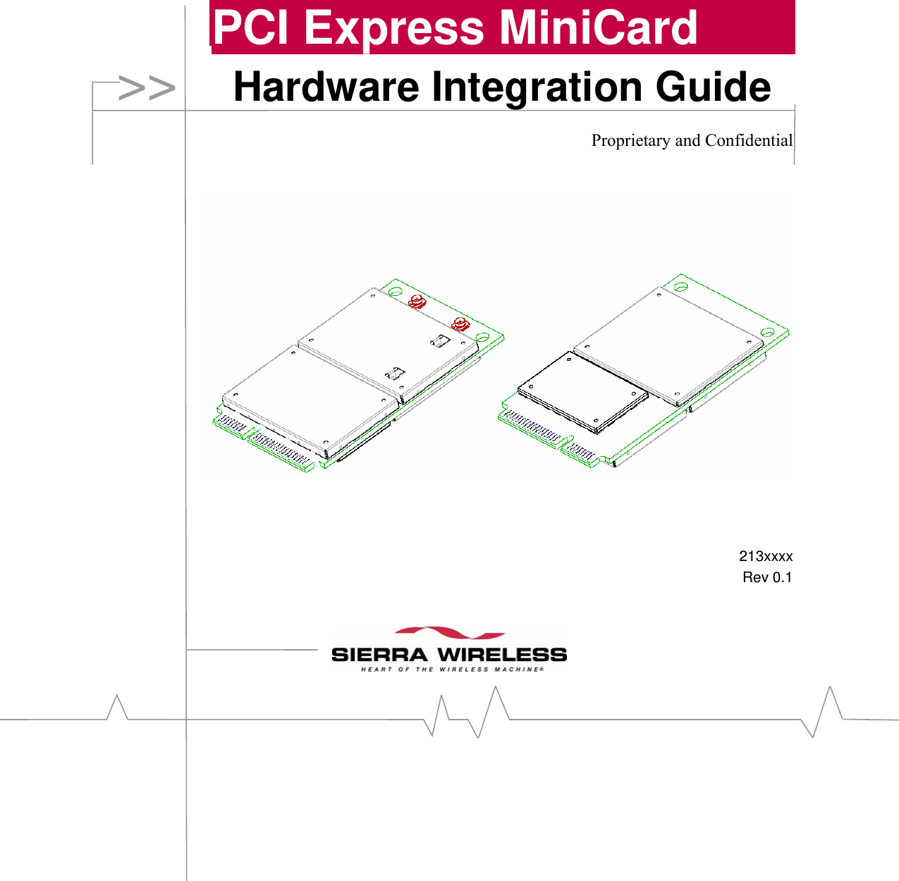
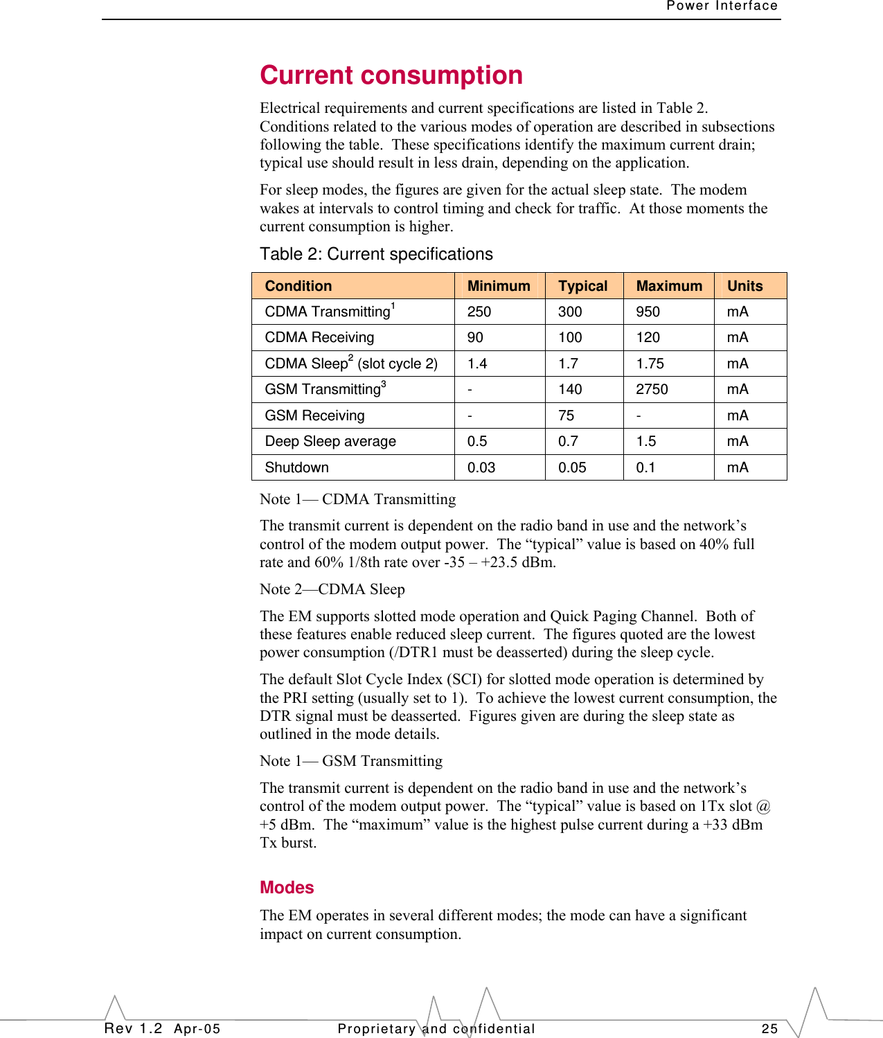
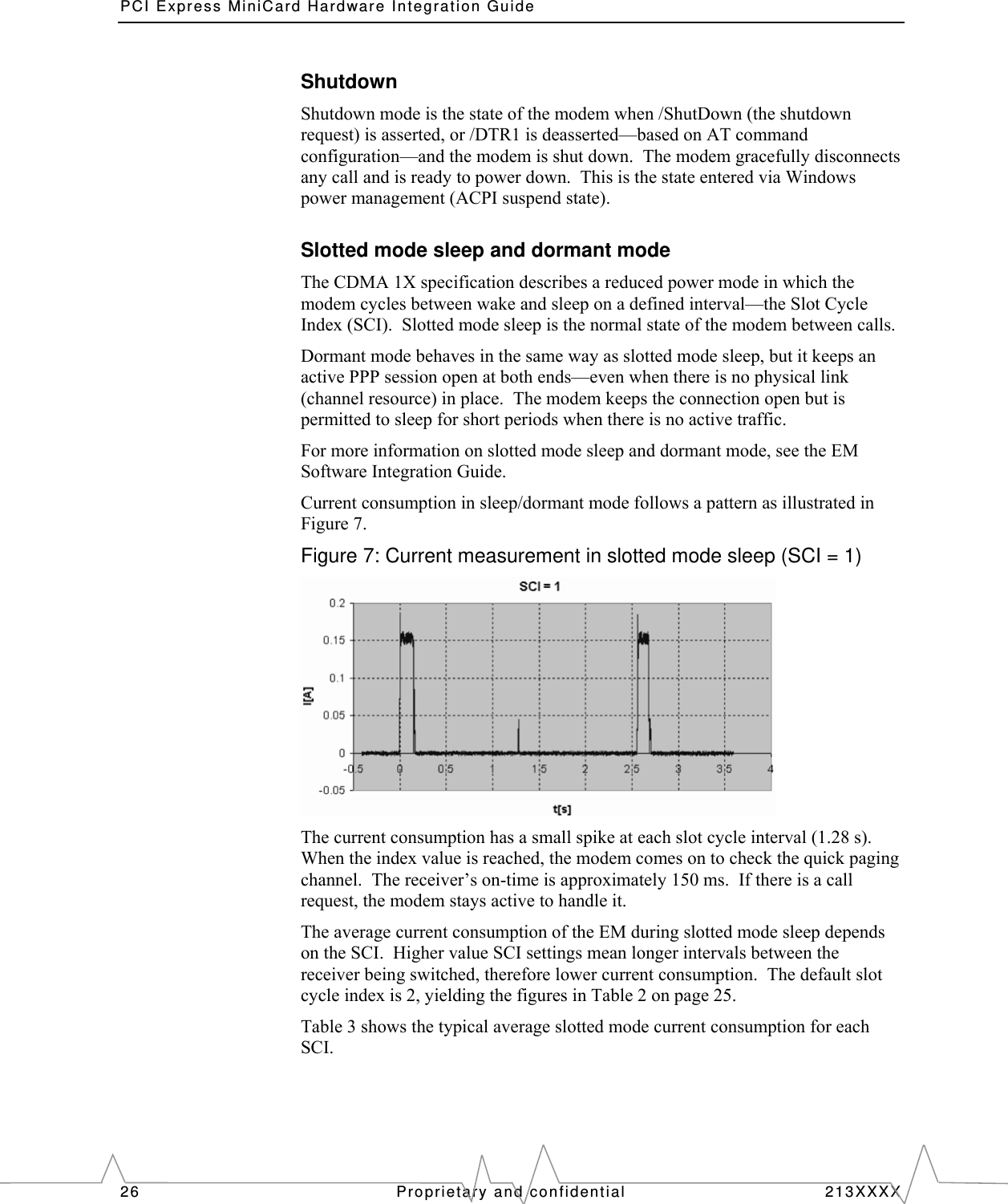
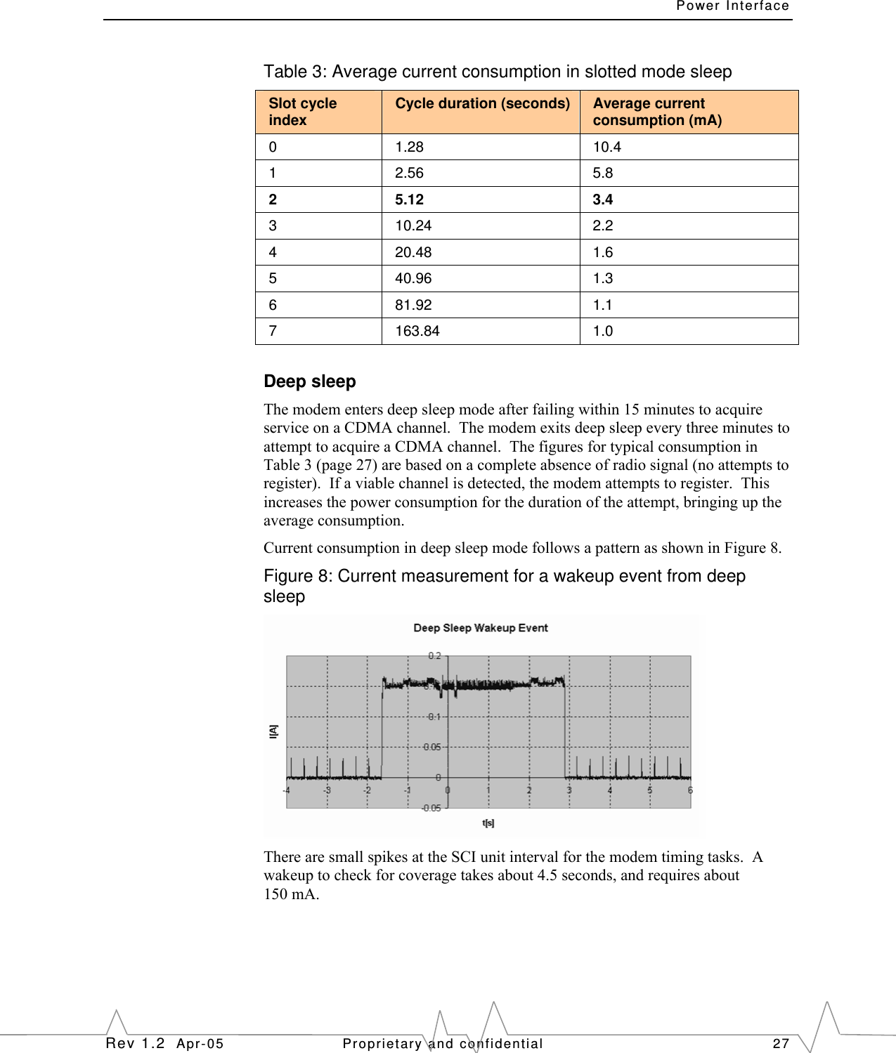
Getac Technology 024 Notebook PC with CDMA800, 1900 User Manual Manual modular transmitter
Getac Technology Corp. Notebook PC with CDMA800, 1900 Manual modular transmitter
UserManual.wiki
>
Getac Technology
>
024 User Manual
>
Manual modular transmitter
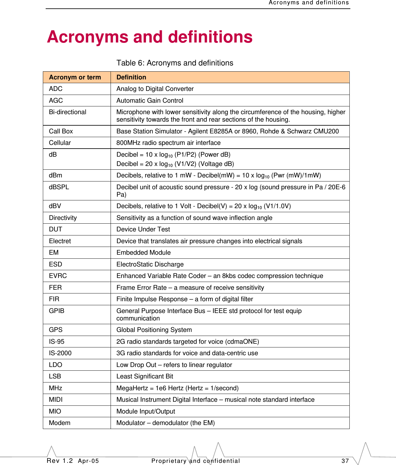
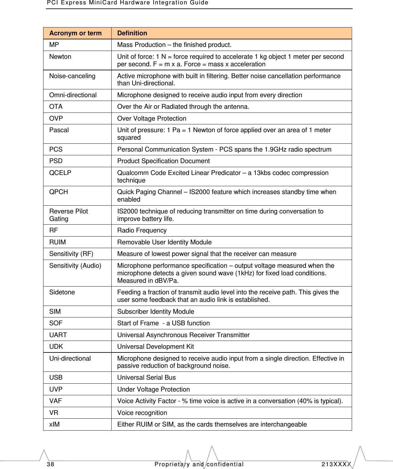
Contents
1.
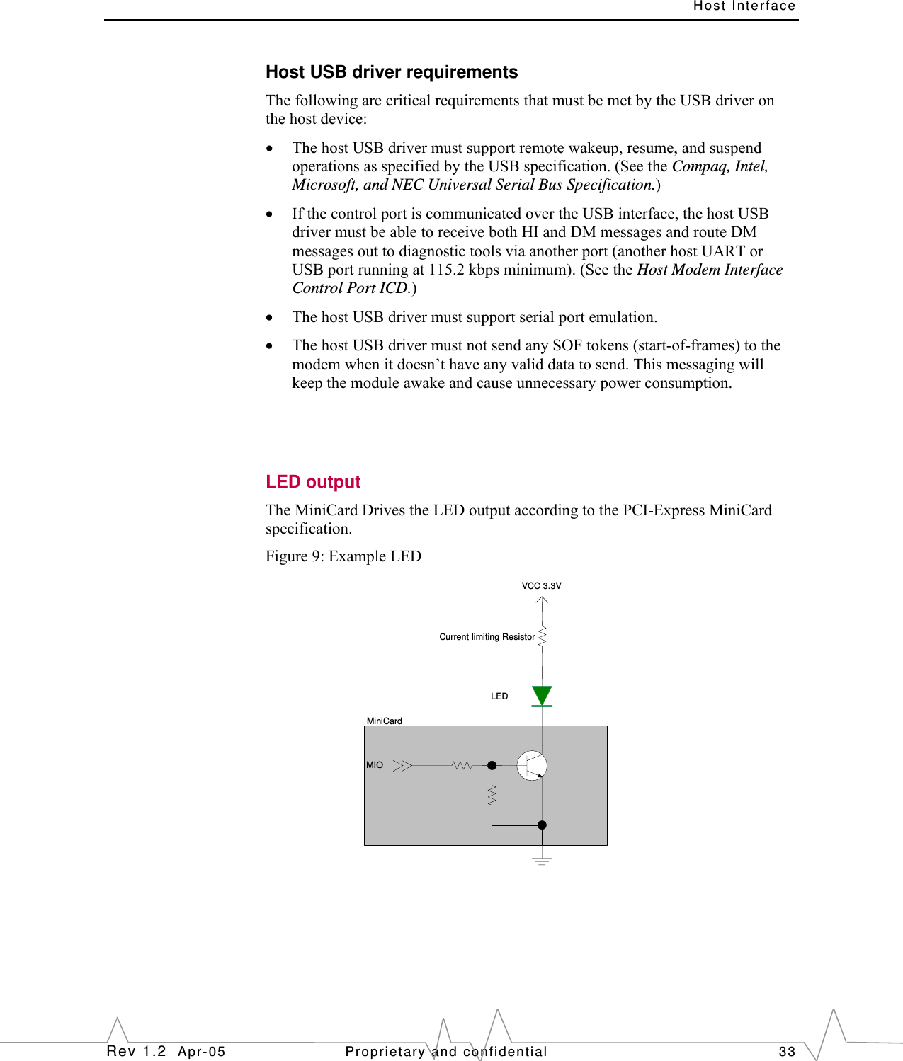
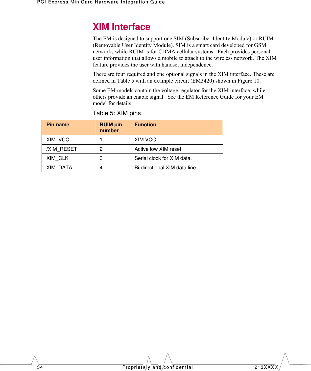
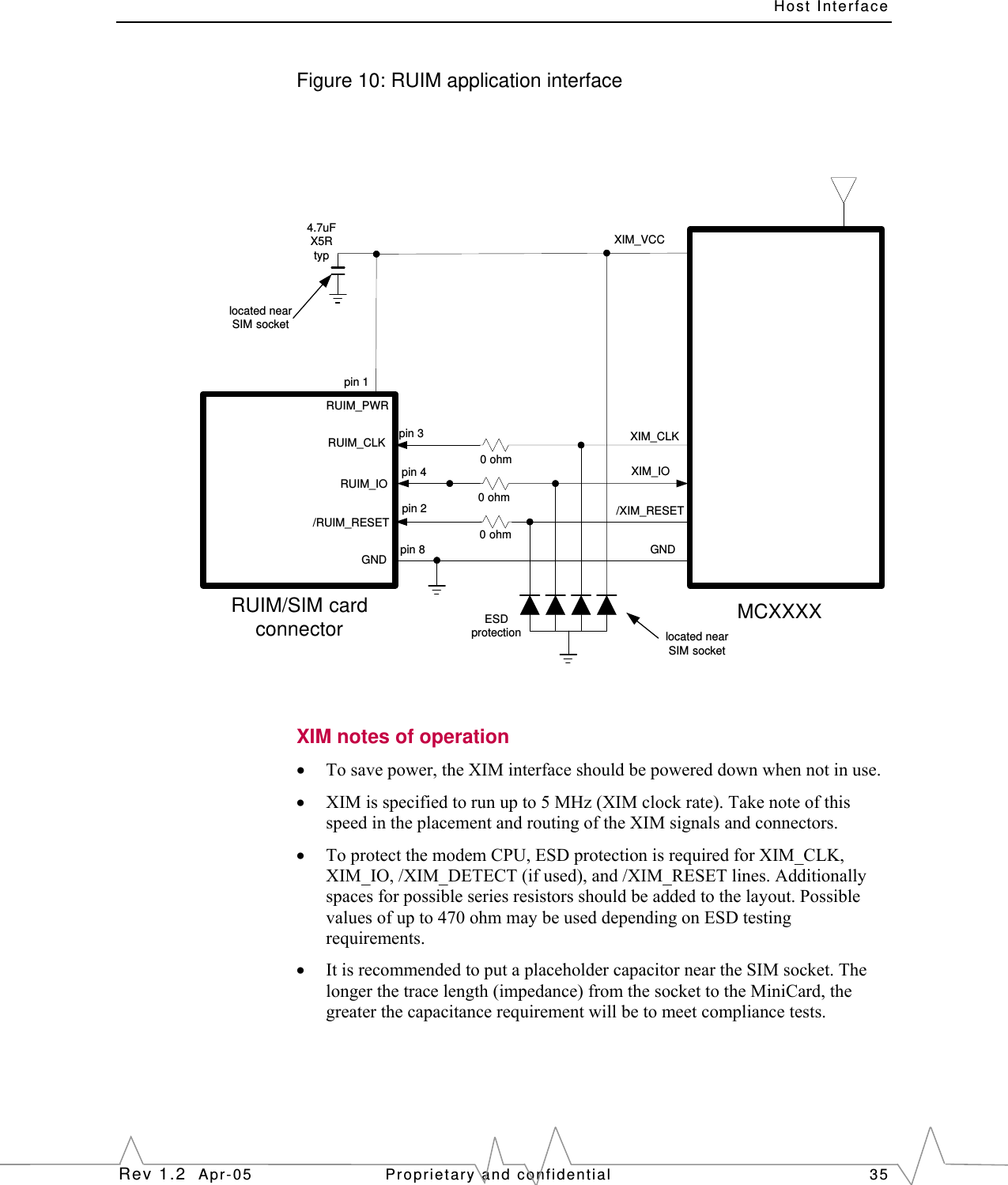
Manual modular transmitter
2.
Manual
Manual modular transmitter
Navigation menu
Upload a User Manual
Namespaces
Wiki Guide
HTML
PDF
Info
Views
User Manual
Discussion / Help
Navigation