Getac Technology 024 Notebook PC with CDMA800, 1900 User Manual Manual modular transmitter
Getac Technology Corp. Notebook PC with CDMA800, 1900 Manual modular transmitter
Contents
- 1. Manual modular transmitter
- 2. Manual
Manual modular transmitter
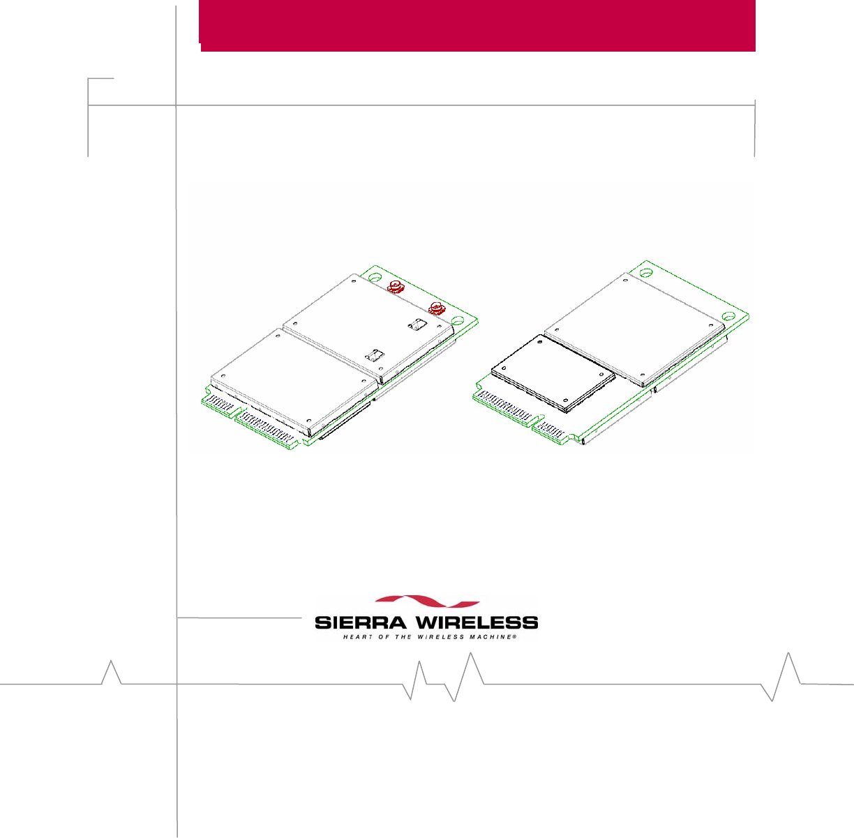
PCI Express MiniCard
Hardware Integration Guide
Proprietary and Confidential
213xxxx
Rev 0.1
>>

PCI Express MiniCard Hardware Integration Guide
2 Proprietary and confidential 213XXXX
Preface
Important notice
Due to the nature of wireless communications, transmission and reception of data
can never be guaranteed. Data may be delayed, corrupted (i.e., have errors) or be
totally lost. Although significant delays or losses of data are rare when wireless
devices such as the Sierra Wireless modem are used in a normal manner with a
well-constructed network, the Sierra Wireless modem should not be used in
situations where failure to transmit or receive data could result in damage of any
kind to the user or any other party, including but not limited to personal injury,
death, or loss of property. Sierra Wireless accepts no responsibility for damages
of any kind resulting from delays or errors in data transmitted or received using
the Sierra Wireless modem, or for failure of the Sierra Wireless modem to
transmit or receive such data.
Safety and hazards
Do not operate the Sierra Wireless modem in areas where blasting is in progress,
where explosive atmospheres may be present, near medical equipment, near life
support equipment, or any equipment which may be susceptible to any form of
radio interference. In such areas, the Sierra Wireless modem MUST BE
POWERED OFF. The Sierra Wireless modem can transmit signals that could
interfere with this equipment.
Do not operate the Sierra Wireless modem in any aircraft, whether the aircraft is
on the ground or in flight. In aircraft, the Sierra Wireless modem MUST BE
POWERED OFF. When operating, the Sierra Wireless modem can transmit
signals that could interfere with various onboard systems.
Some airlines may permit the use of cellular phones while the
aircraft is on the ground and the door is open. Sierra Wireless
modems may be used at this time.
The driver or operator of any vehicle should not operate the Sierra Wireless
modem while in control of a vehicle. Doing so will detract from the driver or
operator's control and operation of that vehicle. In some states and provinces,
operating such communications devices while in control of a vehicle is an
offence.
Limitation of liability
The information in this manual is subject to change without notice and does not
represent a commitment on the part of Sierra Wireless. SIERRA WIRELESS
AND ITS AFFILIATES SPECIFICALLY DISCLAIM LIABILITY FOR ANY
AND ALL DIRECT, INDIRECT, SPECIAL, GENERAL, INCIDENTAL,
CONSEQUENTIAL, PUNITIVE OR EXEMPLARY DAMAGES INCLUDING,
BUT NOT LIMITED TO, LOSS OF PROFITS OR REVENUE OR
ANTICIPATED PROFITS OR REVENUE ARISING OUT OF THE USE OR
Preface
Rev 1.2 Apr-05 Proprietary and confidential 3
INABILITY TO USE ANY SIERRA WIRELESS PRODUCT, EVEN IF
SIERRA WIRELESS AND/OR ITS AFFILIATES HAS BEEN ADVISED OF
THE POSSIBILITY OF SUCH DAMAGES OR THEY ARE FORESEEABLE
OR FOR CLAIMS BY ANY THIRD PARTY.
Notwithstanding the foregoing, in no event shall Sierra Wireless and/or its
affiliates aggregate liability arising under or in connection with the Sierra
Wireless product, regardless of the number of events, occurrences, or claims
giving rise to liability, be in excess of the price paid by the purchaser for the
Sierra Wireless product.
Patents
Portions of this product are covered by some or all of the following US patents:
5,515,013 5,617,106 5,629,960 5,682,602 5,748,449
5,845,216 5,847,553 5,878,234 5,890,057 5,929,815
6,169,884 6,191,741 6,199,168 6,327,154 6,339,405
6,359,591 6,400,336 6,643,501 6,516,204 6,561,851
6,653,979 D367,062 D372,248 D372,701 D416,857
D442,170 D452,495 D452,496 D453,733 D459,303
and other patents pending.
This product includes
technology licensed from
QUALCOMM Incorporated under one or more of the following United States patents and/or
their counterparts in other nations:
4,901,307 5,056,109 5,101,501 5,109,390 5,228,054
5,267,261 5,267,262 5,337,338 5,414,796 5,416,797
5,490,165 5,504,773 5,506,865 5,511,073 5,535,239
5,544,196 5,568,483 5,600,754 5,657,420 5,659,569
5,710,784 5,778,338
Copyright
©2005 Sierra Wireless. All rights reserved.
Trademarks
“Heart of the Wireless Machine” is registered trademark of Sierra Wireless.
Sierra Wireless, the Sierra Wireless logo, the red wave design, the red-tipped
antenna, and Watcher are trademarks of Sierra Wireless.
Windows® is a registered trademark of Microsoft Corporation.
Qualcomm® is a registered trademark of Qualcomm Incorporated.
Other trademarks are the property of the respective owners.

PCI Express MiniCard Hardware Integration Guide
4 Proprietary and confidential 213XXXX
Comments
Sales Desk: Phone: 1-604-232-1488
Hours: 8:00
AM to 5:00 PM Pacific Time
E-mail: sales@sierrawireless.com
Post: Sierra Wireless
13811 Wireless Way
Richmond, BC
Canada V6V 3A4
Fax: 1-604-231-1109
Web: www.sierrawireless.com
Your comments and suggestions on improving this documentation are welcome
and appreciated. Please e-mail your feedback, noting document 2130367 Rev 1.1,
to documentation@sierrawireless.com. Thank you.
Consult our website for up-to-date product descriptions, documentation,
application notes, firmware upgrades, troubleshooting tips, and press releases:
www.sierrawireless.com

Preface
Rev 1.2 Apr-05 Proprietary and confidential 5
Table of Contents
Preface..........................................................................................................................................2
Important notice ................................................................................................................2
Safety and hazards ...........................................................................................................2
Limitation of liability...........................................................................................................2
Patents..............................................................................................................................3
Copyright...........................................................................................................................3
Trademarks.......................................................................................................................3
Comments.........................................................................................................................4
Introduction ...................................................................................................................................9
The Universal Development Kit.........................................................................................9
Document organization ...................................................................................................10
RF Integration .............................................................................................................................11
RF connection.................................................................................................................11
Ground connection ..............................................................................................11
Shielding..............................................................................................................12
Ground plane isolation ........................................................................................12
Antenna and cabling............................................................................................12
Interference and sensitivity .............................................................................................13
Power supply noise .............................................................................................13
Device-generated RF ..........................................................................................13
RF desense mitigation.........................................................................................13
Hearing aid considerations..................................................................................14
Radiated sensitivity measurement ..................................................................................14
Physical configuration .........................................................................................14
Path loss calculation............................................................................................15
Positioning the DUT (Device Under Test) ...........................................................15
Sensitivity vs. frequency......................................................................................16
Regulatory information ....................................................................................................17
FCC module acceptance criteria.....................................................................................17
FCC classification of mobile vs. portable devices ...............................................17
RF exposure requirements for mobile approval ..................................................18
Product labeling requirements.............................................................................18

PCI Express MiniCard Hardware Integration Guide
6 Proprietary and confidential 213XXXX
Power Interface...........................................................................................................................20
Overview of operation .....................................................................................................20
EM power signals ................................................................................................20
Electrostatic discharge ........................................................................................20
EM power state transitions..............................................................................................21
DISCONNECTED state.......................................................................................21
OFF state ............................................................................................................21
NORMAL state ....................................................................................................21
LOW BATTERY state..........................................................................................21
SHUTDOWN ROUTINE state .............................................................................22
EMERGENCY SHUTDOWN state ......................................................................22
Inrush currents ................................................................................................................22
Current consumption.......................................................................................................25
Modes..................................................................................................................25
Shutdown.................................................................................................26
Slotted mode sleep and dormant mode...................................................26
Deep sleep...............................................................................................27
Usage models .....................................................................................................28
Back-power issues..........................................................................................................28
Preventing back-power when the modem is off...................................................28
Host Interface..............................................................................................................................29
Operation modes.................................................................................................29
USB interface..................................................................................................................29
Physical layer...........................................................................................30
POWER and RESET handshaking protocols ..........................................31
USB handshaking................................................................................................32
Suspending..............................................................................................32
Resume ...................................................................................................32
Host USB driver requirements.................................................................33
LED output ..........................................................................................................33
XIM Interface...................................................................................................................34
XIM notes of operation ........................................................................................35
Acronyms and definitions............................................................................................................37

Preface
Rev 1.2 Apr-05 Proprietary and confidential 7
Figures
Figure 1: Anechoic chamber........................................................................................... 15
Figure 2: US PCS sensitivity measurements .................................................................. 16
Figure 3: Power state transition diagram ........................................................................ 21
Figure 4: Inrush model.................................................................................................... 22
Figure 5: Inrush without large decoupling capacitors...................................................... 24
Figure 6: Inrush with 66µF decoupling capacitors .......................................................... 24
Figure 7: Current measurement in slotted mode sleep (SCI = 1) ................................... 26
Figure 8: Current measurement for a wakeup event from deep sleep............................ 27
Figure 20: Example LED................................................................................................. 33
Figure 34: RUIM application interface............................................................................. 35

PCI Express MiniCard Hardware Integration Guide
8 Proprietary and confidential 213XXXX
Tables
Table 1: Typical RF parameters for a CDMA Embedded Module................................... 11
Table 2: Current specifications ....................................................................................... 25
Table 3: Average current consumption in slotted mode sleep........................................ 27
Table 4: Power consumption of a sample application..................................................... 28
Table 32: XIM pins.......................................................................................................... 34
Table 39: Acronyms and definitions................................................................................ 37

Introduction
Rev 1.2 Apr-05 Proprietary and confidential 9
Introduction
Sierra Wireless manufactures several modules that are designed to be embedded
in other products, such as mobile phones and PDAs (Personal Digital Assistants).
The Sierra Wireless modules form the radio component of these products,
providing the ability to establish wireless phone calls and/or data connections.
There are several models of these embedded modules, including:
• The MC5720 which operates on CDMA networks using the IS-95A and
CDMA 1x, and EvDO (IS-866) network standards
• The MC8755 which operates on GSM networks using the
GSM/GPRS/EDGE/W-CMDA/HSDPA network standards
• Other modules under development that will operate using other network
standards.
Typically, integrating an embedded module into another product has these
phases:
1. Embedded module evaluation—The capabilities of the EM are evaluated,
and an interface strategy is developed.
2. Interface development—The host software is designed using the
appropriate communications protocols and control signal sequencing.
3. Embedded module integration—A probe-ready connection is created
between the embedded module and the host product.
This guide is concerned with the third phase of integration and provides the
information necessary to create a connection between the embedded module and
the host product. Recommendations related to the host design are also provided.
An understanding of network technology and experience in integrating hardware
components into electronic equipment is assumed.
The Universal Development Kit
Sierra Wireless manufactures a Universal Development Kit (UDK) that
facilitates all phases of the integration process. The UDK is based on a
development platform that is designed to support multiple members of the
Wireless Embedded Module (EM) product family. For more information, see the
Universal Development Kit Hardware User Guide.

PCI Express MiniCard Hardware Integration Guide
10 Proprietary and confidential 213XXXX
Document organization
This document is organized into the following sections:
1. Introduction (this section)
2. RF Integration (page 11)—Discusses antenna connection methods and
grounding issues, and describes how to design the host in order to minimize
RF interference and desense issues as well as noise from other components.
This section also discusses regulatory approvals and regulatory information
requirements.
Note: The RF integration section is placed at the front of this
guide to emphasize the importance of designing the shielding to
minimize isolation issues. Having RF design issues an
afterthought of product design often results in compromised
performance and failure to meet release schedules.
3. Power Interface (page 20)—Describes the power control signals used by the
embedded module and discusses design issues related to battery use.
4. Host Interface (page 29)—Details the control signals available to the host.
Note: In this document, the terms “modem”, “module”, “PCI
Express MiniCard”, and “MiniCard” all refer to the embedded
module (EM) and are used interchangeably. The term “host”
always refers to the host device.
5. XIM Interface (page 34)—Describes how to implement a SIM/RUIM card
interface on the host.
6. (page 36)—Explains how to measure talk and standby currents in the
product, and how these relate to advertised talk and standby times.
Note: Throughout this document, signal directions in each table
are taken from the module’s perspective.
RF Integration
Rev 1.2 Apr-05 Proprietary and confidential 11
RF Integration
This chapter provides information related to the RF (Radio Frequency)
integration of the EM. The frequencies of operation and performance
specifications vary depending on the EM model used. RF performance
parameters for a typical EM are listed below.
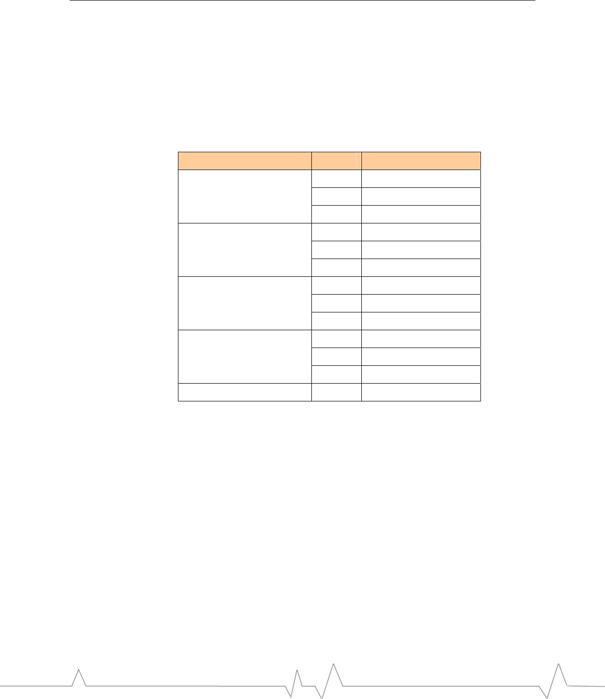
Table 1: Typical RF parameters for a CDMA Embedded Module
Parameter Band Value
PCS 1851 to 1910 MHz
Cellular 824 to 849 MHz
Transmit Band
IMT 1920 to 1980 MHz
PCS +24.0 dBm (251 mW)
Cellular +24.0 dBm (251 mW)
Maximum Transmit Power
IMT +23.0 dBm (200 mW)
PCS 1930 to 1990 MHz
Cellular 869 to 894 MHz
Receiver Band
IMT 2110 to 2170 MHz
PCS >-106 dBm
Cellular >-106 dBm
Receiver Sensitivity
IMT >-105 dBm
GPS Band 1575.42 MHz
RF connection
You can attach an antenna to the antenna connection point on the embedded
module using the Hirose UFL connector.
Any coaxial connection between the EM and the antenna requires the antenna to
be correctly matched to 50 Ω. Note that additional RF cabling losses affect the
performance values listed in the EM specification.
Ground connection
There needs to be a very god ground connection to the modem through the host
connector. It is recommended that the two mounting holes at the top of the
MiniCard be connected to system ground. The integrator needs to be careful
about noise on the ground getting into the RF. Noise could potentially be coupled
to the module from the host board, depending on the design. This is mainly an
issue for host designs that have signals traveling along the length of the module,
or circuitry operating at both ends of the module interconnects. In some cases if

PCI Express MiniCard Hardware Integration Guide
12 Proprietary and confidential 213XXXX
the noise cannot be reduced, isolating the mounting holes from the ground may
actually help.
Shielding
The module is fully shielded to protect against EMI and to ensure FCC Part 15
(or equivalent) compliance. To maintain the shield effectiveness, the modem
shields must not be removed.
Ground plane isolation
The coaxial cable connecting the module to the antenna carries the ground
connection. To avoid a ground loop, the ground plane for the antenna and the
ground plane used by the modem must be electrically isolated from each other.
If your integration uses the device’s case as part of the ground connection, then,
to avoid creating a ground loop, the external antenna connection must be isolated
from the case.
Antenna and cabling
In selecting the antenna and cable, it is critical to RF performance to match
antenna gain and cable loss.
For proper matching, the antenna along with any associated circuitry should have
a nominal impedance of 50 Ω with a return loss ≤ -10 dB across each frequency
band of operation. Overall system antenna gain, with cable loss, should be
≥ 0 dBi and ≤ +6 dBi. Keep in mind that the system gain value impacts radiated
power and the FCC MPE/SAR (or equivalent) test results.
Many antenna vendors produce dual-band antennas that would work with the
EM. You may instead choose to develop a custom-designed antenna. This
requires a skilled RF engineer to ensure that the RF performance is maintained.
Antenna location may also impact RF performance. The modem itself is shielded
to prevent interference in most applications, but this does not mean that antenna
placement can be ignored.
Any connecting cables between the modem and the antenna (if required) must
have 50 Ω impedance. Mismatching the impedance of the EM will result in a
significant reduction in RF performance.

RF Integration
Rev 1.2 Apr-05 Proprietary and confidential 13
Interference and sensitivity
Several sources of interference could impact the RF performance of the EM.
Common sources are discussed below.
Most carriers require a certain level of receiver performance to ensure proper
functioning of the device on the their networks. Although the EM has been
designed to meet these carrier requirements, it is still susceptible to various
performance inhibitors. As part of the Engineering Services package, Sierra
Wireless offers modem OTA (Over-The-Air) sensitivity testing and
desensitization (desense) investigation. For more information, contact your
account manager or the Sales Desk (see page 4).
Power supply noise
Noise in the power supply can lead to noise in the RF signal. The EM
specification contains limits for power supply ripple, which should be no more
than 200 mVp-p 1 Hz to 100 kHz. This includes voltage ripple due to transmitter
burst activity.
Device-generated RF
All electronic computing devices generate RF interference. You should pay
particular attention to RF noise—it can impact the receive sensitivity of the EM
wireless modem.
The proximity of host electronics to the antenna can have an adverse effect on the
radio’s sensitivity. There are many high-speed devices (in particular the
processor itself) running at frequencies of 10s of MHz. These signals generate
higher order harmonics due to the rapid rise and fall of the clock signal. These
harmonics often fall within the operating frequency band of the EM, causing a
decrease in receiver sensitivity.
For example, on a sub-system running at 40 MHz, the 22nd harmonic falls at 880
MHz, which is within the cellular receive frequency band. In practice, there are
usually numerous interfering frequencies and harmonics. The net effect can be a
series of desensitized receive channels. Most device designers are familiar with
having to pay attention to radiated emissions in order to meet the FCC Part 15 (or
equivalent) rules. The components most likely to cause RF desense are: the
microprocessor and memory, display panel and display drivers, and switching-
mode power supplies.
RF desense mitigation
To mitigate RF desense, some or all of these techniques can be used:
• Locate the antenna as far as possible from sources of interference. The
drawback is that the modem may be less convenient to use.
• Shield the host device. The EM itself is well shielded to avoid interference.
However the antenna cannot be shielded for obvious reasons. In most
instances, it is necessary to employ shielding on the components of the host

PCI Express MiniCard Hardware Integration Guide
14 Proprietary and confidential 213XXXX
device (such as the main processor and parallel bus) that have the highest RF
emissions.
• To filter out unwanted high-order harmonic energy, use discrete filtering on
low frequency lines.
• To form shielding layers around high-speed clock traces, use multi-layer
PCBs.
It is important to investigate sources of localized interference early in the design
cycle.
Hearing aid considerations
Just as outside frequencies can interfere with the modem’s sensitivity, the modem
can cause noise in hearing aids due to the keying of the transmitter.
Most digital wireless technologies do not transmit radio frequencies
continuously. They transmit in bursts, usually of specific durations, referred to as
RF burst frequencies.
Unfortunately, most hearing aids are not immuned to RF; they convert the burst
frequencies into audible frequencies. This causes unpleasant noise for hearing aid
users in close proximity to transmitters, as is the case with digital wireless
phones.
Radiated sensitivity measurement
A wireless device contains many sources of noise, such as the LCD, the digital
processor and memory, and any high-speed digital bus (due to the fast rise and
fall times of the digital signals). These sources can generate noise over a wide
range of frequencies, with significant energy in the receive band. If noise
generated in the receive band is allowed to radiate from the device and the
antenna detects it, the noise may mask low-level desired signals, thereby
decreasing the sensitivity of the device. To determine the extent of any
desensitization of receiver performance due to self-generated noise in the host
device, Over the Air (OTA) or radiated testing is required.
Physical configuration
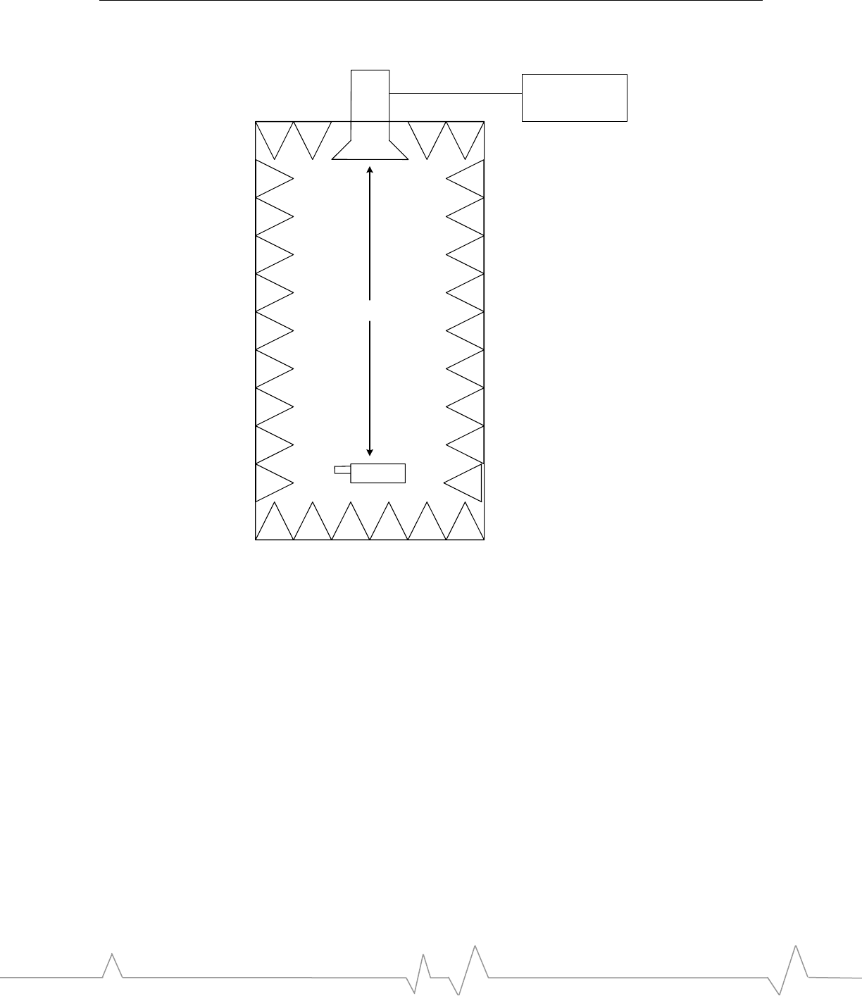
To make OTA measurements, a test chamber is required. A full-size anechoic
chamber is not necessarily required. Figure 1 shows a small anechoic chamber
manufactured by Lindgren. This does not provide power to the same accuracy as
a full-size anechoic chamber, but is sufficient for this application. A base station
simulator, in this case an Agilent 8960, is used to provide FER (Frame Error
Rate) measurements.
RF Integration
Rev 1.2 Apr-05 Proprietary and confidential 15
Figure 1: Anechoic chamber
Approx . 1 m
Agilent 8960
call box
Path loss calculation
The chamber is calibrated for path loss using a reference antenna with known
gain that is feeding a spectrum analyzer or power meter. This makes it possible to
determine the radiated power available to the receiving antenna, which is equal to
the measured received power, plus any cable losses, minus the gain of the
reference receive antenna. Path loss is then determined by subtracting the input
power. It is not necessary to know the gain of the transmitting antenna; it is
included in the path loss.
Positioning the DUT (Device Under Test)
To achieve meaningful results, the device must be positioned such that the peak
of the receive antenna pattern is pointed toward the source antenna.
Theoretically, the best way to accomplish this is to modify the DUT so that
antenna output is through coaxial cable. The device is then rotated until the
receive power is maximized.
Path loss can also be calculated without modifying the DUT by using the
transmit capabilities of the unit. This method of calculation is possible because
the position that maximizes transmitter power provides a sufficiently accurate
PCI Express MiniCard Hardware Integration Guide
16 Proprietary and confidential 213XXXX
location for receiver desense measurements. The unit is placed in a call and set to
generate peak output power, either through a test mode, or by configuring the
base station simulator to issue the appropriate command. The unit is then
positioned for maximum power as determined by the call box.
Sensitivity vs. frequency
Sensitivity is defined as the input power level in dBm that produces a FER of
.5%. Sensitivity should be measured at all CDMA frequencies across the band. In
the US PCS band for example, there are 25 physical channels with a spacing of
50 KHz. The first CDMA channel is CH25.
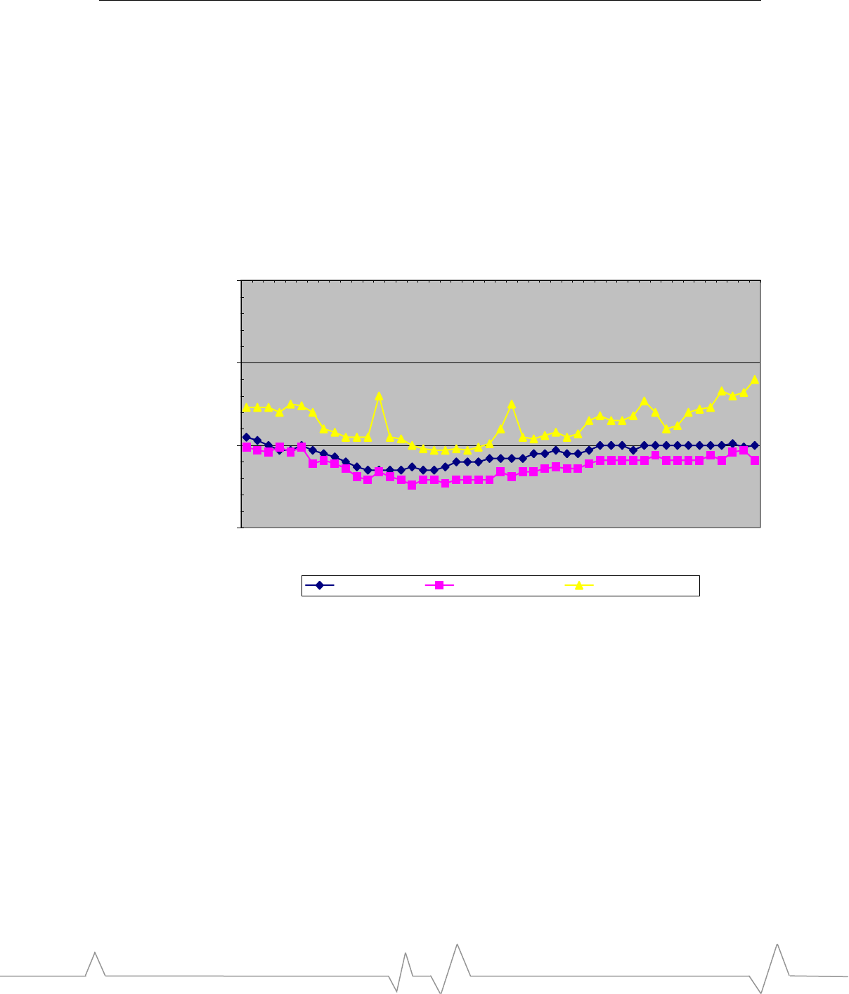
Figure 2: US PCS sensitivity measurements
-110
-105
-100
-95
25
75
125
175
225
275
325
375
425
475
525
575
625
675
725
775
825
875
925
975
1025
1075
1125
1175
Channel
Sensitivity dBm
Connectorized OTA, Ext Antenna OTA, Int Antenna
Figure 2 shows typical test results for the US PCS band for both conducted and
over-the-air connections. The conducted (or “connectorized”) measurements
were made using an RF coaxial cable connection. The over-the-air measurements
were made using both an external antenna and a typical device antenna.
In this test, the external antenna performed best—the expected result if a high
efficiency antenna with some gain is used. The internal antenna has less gain than
the external antenna, so the internal antenna’s performance is offset above the
external antenna. The antenna gain must be known to determine whether the
offset is strictly the result of antenna gain or if broadband desense is present.
Narrowband desense can be seen at channels 325, 625, and 925.

RF Integration
Rev 1.2 Apr-05 Proprietary and confidential 17
Regulatory information
Refer to the EM Reference Guides for Regulatory Information. Regulatory
compliance information is dependent upon both the individual module
certification as well as the intended market.
FCC module acceptance criteria
FCC classification of mobile vs. portable devices
For operation in the United States, your module integration is required to meet
certain regulatory requirements for stand-alone operation, including 47 CFR
Parts 2, 15, 22, and 24.
Part 15 testing must be performed on the “complete device” that has incorporated
the EM and is therefore your responsibility.
The Office of Engineering and Technology has published a document entitled
“Evaluating Compliance with FCC Guidelines for Human Exposure to
Radiofrequency Electromagnetic Fields”, OET Bulletin 65. This provides a
detailed description of the difference between mobile and portable devices.
The FCC Guidelines differentiate between these devices according to the
antenna’s proximity to people, either the user or others nearby.
Mobile: The FCC defines a mobile device as being designed for use “in other
than fixed locations and to generally be used in such a way that a separation
distance of at least 20 centimeters is maintained between radiating structures and
the body of the user or nearby persons”.
Mobile devices including vehicle-mounted systems are designed to be used by
people that are typically well separated from the antenna. This also includes
wireless devices associated with a personal computer, provided the antenna is
kept 20 centimeters away from the body.
These devices are normally evaluated for exposure potential with relation to
MPE (Maximum Permissible Exposure) limits. The FCC rules for evaluating
mobile devices for RF compliance are found in 47 CFR Part 2.1091 (b).
Portable: A portable device has a transmitter “designed to be used with any part
of its radiating structure in direct contact with the user’s body or within 20
centimeters of the user or bystander under normal operating conditions.”
This category includes hand held cellular telephones with antennas built into the
device.
Portable devices are evaluated with respect to SAR (Specific Absorption Rate)
rules. These can be found in 47 CFR Part 2.1093 (b).

PCI Express MiniCard Hardware Integration Guide
18 Proprietary and confidential 213XXXX
RF exposure requirements for mobile approval
Certain Sierra Wireless embedded modules have been approved for mobile
operations only in accordance to 47 CFR Part 2.1091 (b). The Reference Guide
for your EM model contains the FCC ID Number if approved.
Warning: If this module will be used as a portable device, you are
responsible for separate approval to satisfy the SAR requirements
of 47 CFR Part 2.1093 (b).
To ensure the module meets the current FCC exposure
guidelines, a separation distance of at least 20 cm must be
maintained between the module’s antenna and the body of the
user and any nearby person at all times and in all applications and
uses. Additionally, in mobile applications, maximum antenna gain
must not exceed 6.0 dBi (or less, depending on actual FCC grant
verbiage) in order to comply with FCC regulations limiting both
maximum RF output power and human exposure to RF radiation.
Product labeling requirements
For mobile devices, using the FCC approval obtained by Sierra Wireless, a label
must be attached to the outside of your product- into which the authorized
module is incorporated- with a statement similar to the following:
“This device contains TX FCC ID: N7N-XXXXX”
Note: Sierra Wireless can provide specific FCC ID numbers for
each particular EM that has completed module level certification
testing.
You will also need to provide a manual with your end product that clearly states
the operating requirements and conditions that must be observed to ensure
compliance with current FCC RF exposure guidelines (as detailed above).
The warnings must appear in a prominent location in the User Guide for your
product and may include the following text:
Caution: Unauthorized modifications or changes not expressly
permitted by the manufacturer could void compliance with
regulatory rules, and thereby your authority to use this device.
Warning (EMI): This equipment has been tested and found to
comply with the limits pursuant to Part 15 of the FCC rules.
These limits were designed to provide reasonable protection
against harmful interference in an appropriate installation. This
equipment generates, uses, and can radiate radio frequency
energy and, if not installed and used in accordance with the
instructions, may cause harmful interference to radio
communications. However, there is no guarantee that
interference will not occur in a particular installation.

Rev 1.2 Apr-05 Proprietary and confidential 19
If this equipment does cause harmful interference to radio and
television reception, which can be determined by turning the
equipment off and on, the user is encouraged to try to correct the
interference by one or more of the following suggestions:
• Reorient or relocate the receiving antenna
• Increase the separation between the equipment and receiver
• Connect the equipment into an outlet on a circuit different
from that to which the receiver is connected
• Consult the dealer or an experienced radio/TV technician for
help

PCI Express MiniCard Hardware Integration Guide
20 Proprietary and confidential 213XXXX
Power Interface
Overview of operation
The EM is designed to run off the same power supply as the host system
(typically 3.3V). There is neither an independent power supply within the EM
nor any protection circuits to guard against electrical issues. It is the
responsibility of the host system to provide safe and continuous power to the EM
at all times.
The EM powers on when W_Disable# is floated or driven high, and valid power
is applied to the VCC rail. Once turned on by the host system, the EM remains on
until the host commands the module to power down. Once the unit is powered
off, the host can turn the unit on again. The EM unit monitors its voltage and
informs the host if the power rail gets too low by requesting shutdown.
EM power signals
shows the signals comprising the host-EM power interface. A sample schematic
of the interface and BOM (Bill of Materials) are shown on the following page.
See the Product Specification document for your module for detailed
specifications on the power signals.
Electrostatic discharge
You are responsible for any ESD protection on digital circuits. Specific
recommendations are provided as needed for each of the interfaces described in
this guide; however, the level of protection required depends on your application.
For ESD protection level of the EM pins during your product assembly and test,
refer to the EM Product Specification.
Extra precaution should be taken on the U-SIM/R-UIM signals as these signals
are usually brought out externally and are susceptible to ESD events. ESD
protection is recommended at the point where the contacts are exposed.

Power Interface
Rev 1.2 Apr-05 Proprietary and confidential 21
EM power state transitions
Figure 3 shows how the EM transitions between power states. Each power state
is described in the sections that follow.
Figure 3: Power state transition diagram
DISCONNECTED state
This power state occurs when the host power supply is disconnected from the
EM. In this state, all voltages associated with the EM are at 0 V and the host may
or may not be powered off. If the host and the EM share the same battery power
rail, then both the host and EM unit are powered off in this state. If the host
controls the connection between the EM and the battery power, the host can put
the EM into the disconnected state by cutting power to it.
OFF state
In this power state, the host is powered up and the EM is powered down. The EM
unit defaults to the OFF state when VBATT is first applied in the absence of
ON/OFF control. The host keeps the EM powered off by de-asserting the
ON/OFF signal.
Note: In this state, the VCC_RADIO signal is 0 V out of the EM.
To minimize current leakage and prevent unintentional partial
power-up of the EM, the host should not drive any outputs to the
module at a voltage exceeding VCC_RADIO.
Current draw in this mode is an absolute minimum (not more than 50 µA).
NORMAL state
This is the active state of the EM. The EM is fully powered and capable of
placing and receiving phone calls on the CDMA network. All functional
interfaces to the module are enabled (audio, MIO, serial, and, when used, USB).
VCC_RADIO is driven high by the module at 2. 5~3.0 V, indicating full power
status.
LOW BATTERY state
The EM has detected a low battery condition (VBATT <= 3.4 V) and requests
shutdown from the host via UART messaging. The EM carries on its regular
tasks.

PCI Express MiniCard Hardware Integration Guide
22 Proprietary and confidential 213XXXX
SHUTDOWN ROUTINE state
In this state, the EM has received a request from the host to power down and is
completing its active tasks and initiating the shutdown routine. At the completion
of the shutdown routine, the EM drives its OFF signal high and completely
powers down. To keep the EM powered down, the host should keep ON/OFF de-
asserted.
Note: For the duration of the shutdown routine, the EM asserts
the VCC_RADIO signal. Only upon actual power-down does the
EM de-assert its VCC_RADIO signal.
EMERGENCY SHUTDOWN state
In this state, the EM has detected a critically high or critically low battery supply
and sets an internal timer of 15 sec. If the host sends a shutdown request prior to
the expiration of the timer, the EM enters the shutdown routine state. If the timer
expires prior to the host shutdown command, the module automatically enters the
shutdown routine. If the host fails to assert ON/OFF throughout the EM
automatic shutdown routine, an unintentional power-down/power-up cycle may
occur.
Inrush currents
There are two power events that cause large inrush currents from the host supply
to the EM on the power pins.
One event is the application of the supply to the host. This occurs when the
supply is enabled. This event charges the input decoupling capacitors on the EM
power rail.
Figure 4 shows a model of this event.
Figure 4: Inrush model
Power Interface
Rev 1.2 Apr-05 Proprietary and confidential 23
The second event is more important to module integration, and occurs when the
host asserts the ON/OFF signal to power up the EM. This event enables the
power management system of the EM, charging several internal regulator output
capacitors. Sufficient capacitance must be added to the host power rail to limit
the inrush current and stabilize the supply of power to the EM.
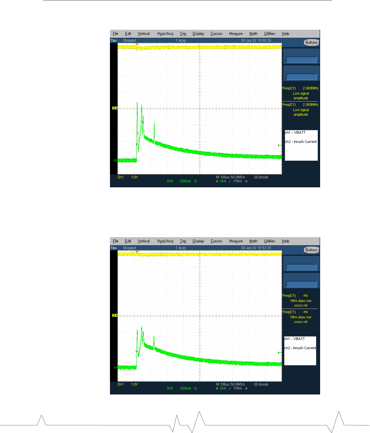
Figure 5 (page 22) and Figure 6 (page 24) show typical inrush current
measurements at room temperature when the host deasserts the W_Disable#
signal to power up the EM. Note that the current spikes are staggered because the
EM internal regulators switch on at slightly different times. In some
circumstances, depending on temperature and the components in use, two or
more regulators may switch on at the same instant. The host power system must
be designed to handle this scenario. Note that the peak current is dictated by the
equation: IPEAK = VBATTERY / RSERIES.
RSERIES is the sum of:
• The path from the positive terminal of the battery to the PWR pins of the EM
to the ground point thru the regulator pass element and output capacitor, and
• The path from the negative terminal of the battery to the GND pins of the
EM regulator
Figure 5 shows a 700 mA inrush from the host battery without the use of large
decoupling caps. A minor dip in VBATT results.
REG
PWR (1,2,3,4,5)
GND
(6,53,54,57,58,59,60)
ON/OFF
(18)
Current
+3.8VDC
LI-ION BATTERY PACK
LI-ION
CELL
250m
LDO pass
element
1 ohm typ
ESR
80m
8.5m 2.8m 1.7m 2.2m
1uF
ESR
20m
ESR
20m
38m
Cin
2x 1uF
10m
32m
Chost
2x 33uF
Current Probe EM BOARD
Regulator input capacitor
Regulator
output
capacitor
ESR +
trace Z
60m
RF Cap
4.7uF
EM board decoupling cap
Host decoupling caps
2x33uF
Cin
2x 1uF
ESR +
trace Z
40m
EM board decoupling cap
15m
PCI Express MiniCard Hardware Integration Guide
24 Proprietary and confidential 213XXXX
Figure 5: Inrush without large decoupling capacitors
Figure 6 shows the effect of increasing decoupling capacitors on the inrush
current (inrush of about 400 mA from the host battery using 66 uF decoupling
caps).
Figure 6: Inrush with 66µF decoupling capacitors
Power Interface
Rev 1.2 Apr-05 Proprietary and confidential 25
Current consumption
Electrical requirements and current specifications are listed in Table 2.
Conditions related to the various modes of operation are described in subsections
following the table. These specifications identify the maximum current drain;
typical use should result in less drain, depending on the application.
For sleep modes, the figures are given for the actual sleep state. The modem
wakes at intervals to control timing and check for traffic. At those moments the
current consumption is higher.
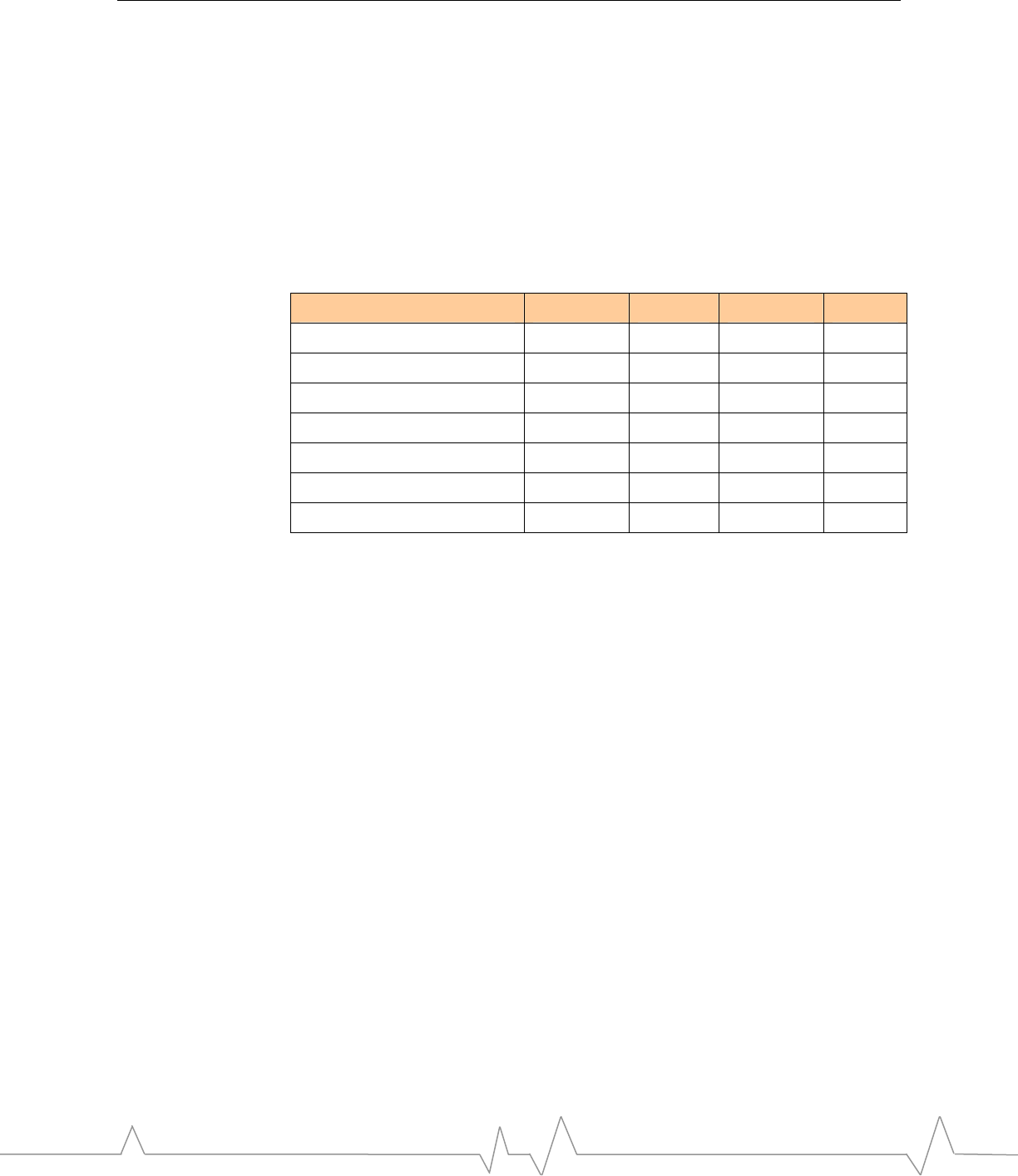
Table 2: Current specifications
Condition Minimum Typical Maximum Units
CDMA Transmitting1 250 300 950 mA
CDMA Receiving 90 100 120 mA
CDMA Sleep2 (slot cycle 2) 1.4 1.7 1.75 mA
GSM Transmitting3 - 140 2750 mA
GSM Receiving - 75 - mA
Deep Sleep average 0.5 0.7 1.5 mA
Shutdown 0.03 0.05 0.1 mA
Note 1— CDMA Transmitting
The transmit current is dependent on the radio band in use and the network’s
control of the modem output power. The “typical” value is based on 40% full
rate and 60% 1/8th rate over -35 – +23.5 dBm.
Note 2—CDMA Sleep
The EM supports slotted mode operation and Quick Paging Channel. Both of
these features enable reduced sleep current. The figures quoted are the lowest
power consumption (/DTR1 must be deasserted) during the sleep cycle.
The default Slot Cycle Index (SCI) for slotted mode operation is determined by
the PRI setting (usually set to 1). To achieve the lowest current consumption, the
DTR signal must be deasserted. Figures given are during the sleep state as
outlined in the mode details.
Note 1— GSM Transmitting
The transmit current is dependent on the radio band in use and the network’s
control of the modem output power. The “typical” value is based on 1Tx slot @
+5 dBm. The “maximum” value is the highest pulse current during a +33 dBm
Tx burst.
Modes
The EM operates in several different modes; the mode can have a significant
impact on current consumption.
PCI Express MiniCard Hardware Integration Guide
26 Proprietary and confidential 213XXXX
Shutdown
Shutdown mode is the state of the modem when /ShutDown (the shutdown
request) is asserted, or /DTR1 is deasserted—based on AT command
configuration—and the modem is shut down. The modem gracefully disconnects
any call and is ready to power down. This is the state entered via Windows
power management (ACPI suspend state).
Slotted mode sleep and dormant mode
The CDMA 1X specification describes a reduced power mode in which the
modem cycles between wake and sleep on a defined interval—the Slot Cycle
Index (SCI). Slotted mode sleep is the normal state of the modem between calls.
Dormant mode behaves in the same way as slotted mode sleep, but it keeps an
active PPP session open at both ends—even when there is no physical link
(channel resource) in place. The modem keeps the connection open but is
permitted to sleep for short periods when there is no active traffic.
For more information on slotted mode sleep and dormant mode, see the EM
Software Integration Guide.
Current consumption in sleep/dormant mode follows a pattern as illustrated in
Figure 7.
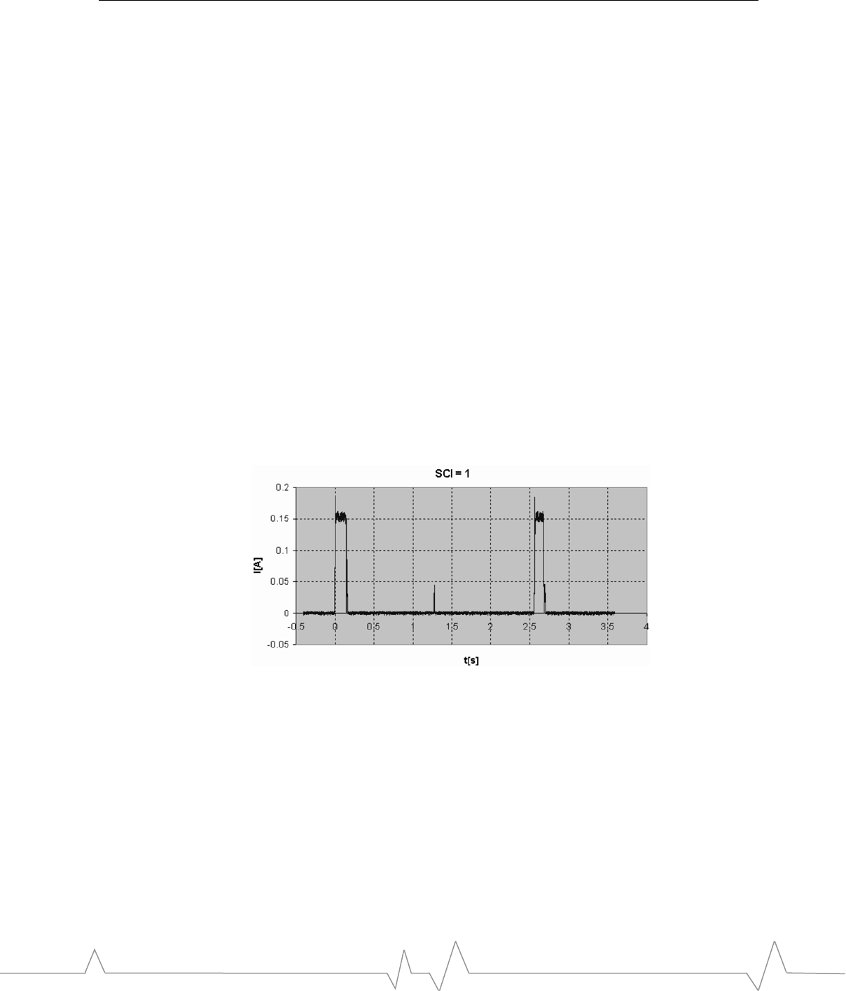
Figure 7: Current measurement in slotted mode sleep (SCI = 1)
The current consumption has a small spike at each slot cycle interval (1.28 s).
When the index value is reached, the modem comes on to check the quick paging
channel. The receiver’s on-time is approximately 150 ms. If there is a call
request, the modem stays active to handle it.
The average current consumption of the EM during slotted mode sleep depends
on the SCI. Higher value SCI settings mean longer intervals between the
receiver being switched, therefore lower current consumption. The default slot
cycle index is 2, yielding the figures in Table 2 on page 25.
Table 3 shows the typical average slotted mode current consumption for each
SCI.
Power Interface
Rev 1.2 Apr-05 Proprietary and confidential 27
Table 3: Average current consumption in slotted mode sleep
Slot cycle
index Cycle duration (seconds) Average current
consumption (mA)
0 1.28 10.4
1 2.56 5.8
2 5.12 3.4
3 10.24 2.2
4 20.48 1.6
5 40.96 1.3
6 81.92 1.1
7 163.84 1.0
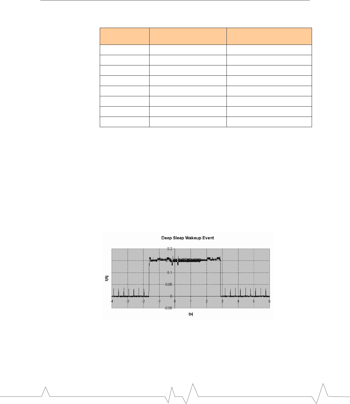
Deep sleep
The modem enters deep sleep mode after failing within 15 minutes to acquire
service on a CDMA channel. The modem exits deep sleep every three minutes to
attempt to acquire a CDMA channel. The figures for typical consumption in
Table 3 (page 27) are based on a complete absence of radio signal (no attempts to
register). If a viable channel is detected, the modem attempts to register. This
increases the power consumption for the duration of the attempt, bringing up the
average consumption.
Current consumption in deep sleep mode follows a pattern as shown in Figure 8.
Figure 8: Current measurement for a wakeup event from deep
sleep
There are small spikes at the SCI unit interval for the modem timing tasks. A
wakeup to check for coverage takes about 4.5 seconds, and requires about
150 mA.

PCI Express MiniCard Hardware Integration Guide
28 Proprietary and confidential 213XXXX
Usage models
To calculate actual current consumption (and anticipated battery life), a usage
model is needed. As applications of the EM can vary widely, we can provide
only samples here.
Slotted mode sleep is assumed when not actively receiving or transmitting (SCI =
2).
Transmit power is assumed to be +3 dBm.
Table 4: Power consumption of a sample application
PDA with voice Field worker
(data only) Remote data
logging
Upload (modem Tx) 20 e-mails / day
avg 5 kB each
1000 kB / day 40 kB / hr
Download (modem Rx) 40 e-mails / day
avg 5 kB each
500 kB web use
500 kB / day 100 kB / day
Coverage / data rate 1x / 80 kbps 1x / 80 kbps IS-95 / 14.4 kbps
Hours of operation 16 / day
(off 8 hrs / day)
8 / day
(off 16 hrs / day)
24 / day
Total power consumed over
24 hours 250 mAh 60 mAh 200 mAh
Back-power issues
Preventing back-power when the modem is off
Note: Without proper input protection, the modem may draw
sufficient current to remain powered, even when the normal
supply power is removed.
Active low signals may be deasserted (driven high) by the host when the modem
is not needed. This applies 3.0 V to the modem on these pins and presents the
risk of back-powering.
All connector inputs must be either high impedance (>20 kohm), or driven low,
when the modem is powered off. This is required to prevent back-powering the
modem.
USB signals can be driven while the modem is disabled.

Host Interface
Rev 1.2 Apr-05 Proprietary and confidential 29
Host Interface
This chapter provides detailed information about the Host-EM interface,
describing the signals required for serial data transfer, handshaking and digital
module I/O (MIO).
Operation modes
The embedded module supports the following logical communication interfaces:
• Data channel—Supports AT command and PPP packet exchange during
data calls
• Control channel—Supports modem control and call processing commands
• Diagnostic channel – Supports modem status and diagnostic logging
USB interface
The USB physical interface is the only path for communication between the host
and modem.
General USB background information can be found in the Compaq, Intel,
Microsoft, and NEC Universal Serial Bus Specification.
The USB interface is designed to comply with the Universal Serial Bus
Specification, Revision 1.1. The EM USB interface supports the full-speed
(12 Mbps) data rate, and can be used to transfer general data, phone diagnostic
data, over-the-air data, or voice PCM samples between the module and a USB
host. The USB interface provides 10 endpoints:
• One bi-directional control endpoint
• Isochronous IN and OUT endpoints for voice
• Four IN endpoints
• Three OUT endpoints
For more background information on USB, see the Compaq, Intel, Microsoft, and
NEC Universal Serial Bus Specification.

PCI Express MiniCard Hardware Integration Guide
30 Proprietary and confidential 213XXXX
Physical layer
Differential 1 and 0
The USB uses differential signaling (called D+ and D-) with NRZI (Non-Return
to Zero, Inverted) encoding. A NRZI encoder toggles the output for input source
data bit 0 and maintains current output state for source data bit 1. A differential 1
exists at the driver when the D+ output is at least 2.8 V and the D- output is no
greater than 0.3 V. A differential 0 exists at the driver when D- is at least 2.8 V
and D+ is no greater than 0.3 V. At the receiver, a differential 1 exists when D+
is at least 2 V, and the difference between D+ and D- is greater than 200 mV. A
differential 0 exists when D- is at least 2 V, and the difference between D- and
D+ is at least 200 mV.
Suspend and resume
The USB master signals "suspend" by not sending the periodic 1 ms SOF for a
minimum of 3 ms.
The USB exits from the suspend state in either of these ways:
• Resume is initiated by the USB master, or
• The USB slave devices initiate remote-wakeup.
Both resume and remote-wakeup generate the resume signaling on the bus.
For more information on USB signal definitions, see the Compaq, Intel,
Microsoft, and NEC Universal Serial Bus Specification.
Suspend and resume
If the USB is not completely powered off and interrupts are still enabled, resume
and suspend interrupts can control the USB’s sleep/wakeup model provided that
the host USB driver supports suspend mode and remote wakeup.
USB_SUSPEND and USB_RESUME interrupts are provided in the
USB_INT_STATUS register (for more detail, see the USB XCVR data sheets.)
Full-speed devices send SOF, which is a timing reference the host sends at 1 ms
intervals. The SOF keeps devices from entering the low-power suspend state
when there is no other USB traffic. Low-speed devices do not see the SOF
packet. Instead, the device's hub translates the SOF to a simpler End-of-Packet
signal called the low-speed keep-alive signal. As the SOF does for full-speed
devices, the low-speed keep-alive keeps low-speed devices from entering the
suspend state. Note that the EM is a full-speed device.
The USB controller automatically enters suspend mode when the USB bus has
been idle for 3 ms. No more than 500 µA current can be drawn from the bus
when in the suspend state. This is indicated by the USB_SUSPEND interrupt.
The current suspend status of the USB is checked through the USB_RUNNING
bit of USB_CORE_STATUS. When the USB controller enters the suspend state,
the modem is able to shut down the 48 MHz oscillator to save power.

Host Interface
Rev 1.2 Apr-05 Proprietary and confidential 31
USB activity is resumed either by the USB host or by the modem. The USB
controller automatically detects the USB host resuming bus activity, even if the
48 MHz oscillator is disabled. This is indicated by the resume interrupt. When
the resume interrupt is detected, the modem must re-enable the 48 MHz oscillator
for the USB controller. If the modem is initiating the resume via remote wakeup,
the 48 MHz oscillator must first be re-enabled. Then the modem directs the USB
controller to resume USB activity by writing the RESUME command (0x02) to
USB_CONTROL_CMD.
POWER and RESET handshaking protocols
This section describes the power-up and power-down on the embedded module.
Power on
The power-on sequence is shown in on page 31. The letters in the figure
correspond to these events:
A. VCC_3V3 is asserted,.
B. The host deasserts the W_Disable# signal to power up the module.
Power off
The power off sequence is shown in on page 31. The letters in the figure
correspond to these events:
A. The host sends the module the AT command to prepare for power down.
(See the EM AT Command Reference).
B. The module performs any necessary housekeeping functions and then
responds to the message.
C. W_Disable# should be asserted by the host.

PCI Express MiniCard Hardware Integration Guide
32 Proprietary and confidential 213XXXX
USB handshaking
The module behaves as a non-host device supporting full-speed USB.
Consequently, the host that interfaces to the module must act as a USB host
device. The module does not use discrete hardware signals for handshaking;
instead the USB standard Resume and Suspend functions are used to control the
sleep and wakeup states. Detailed specifications for the Resume and Suspend
functions can be found in the USB specification in the Compaq, Intel, Microsoft,
and NEC, Universal Bus Specification.
EM modules are either equipped with an on-board USB transceiver, or provide
the interface to a USB transceiver. This section covers both types of EM
modules.
NOTE: The host USB driver must not send start-of-frames when
the modem or host have no data to send. This causes modem
wake-ups and adversely impacts current consumption of the
module.
Suspending
A USB controller automatically enters suspend mode when the USB bus has
been idle for 3 ms. The USB controller triggers the USB_SUSPEND interrupt to
the module’s processor and the module shuts down the 48 MHz clock to save
power.
While in the suspend state, the module provides power to the D+/- interface to
signal to the host device of its current state. During the Suspend state, the host
must maintain the VCC_3V3 voltage. The SOFTCON interface signal is also
maintained during suspend.
Critical timing parameters for the suspend state can be found in the Compaq,
Intel, Microsoft, and NEC Universal Serial Bus Specification.
Resume
USB activity may be resumed by either the USB host or by the module. If the
host initiates USB activity the USB transceiver detects the change in bus activity
and triggers the USB_RESUME interrupt to the module’s processor. The module
then enables its USB clock and responds to the host.
If the module initiates USB communication, it must first enable its USB clock,
enable the USB transceiver, and then send the resume signal for at least 20 ms.
(See the Compaq, Intel, Microsoft, and NEC Universal Serial Bus Specification.)
Critical timing parameters for the resume state can be found in the Compaq,
Intel, Microsoft, and NEC Universal Serial Bus Specification.
Host Interface
Rev 1.2 Apr-05 Proprietary and confidential 33
Host USB driver requirements
The following are critical requirements that must be met by the USB driver on
the host device:
• The host USB driver must support remote wakeup, resume, and suspend
operations as specified by the USB specification. (See the Compaq, Intel,
Microsoft, and NEC Universal Serial Bus Specification.)
• If the control port is communicated over the USB interface, the host USB
driver must be able to receive both HI and DM messages and route DM
messages out to diagnostic tools via another port (another host UART or
USB port running at 115.2 kbps minimum). (See the Host Modem Interface
Control Port ICD.)
• The host USB driver must support serial port emulation.
• The host USB driver must not send any SOF tokens (start-of-frames) to the
modem when it doesn’t have any valid data to send. This messaging will
keep the module awake and cause unnecessary power consumption.
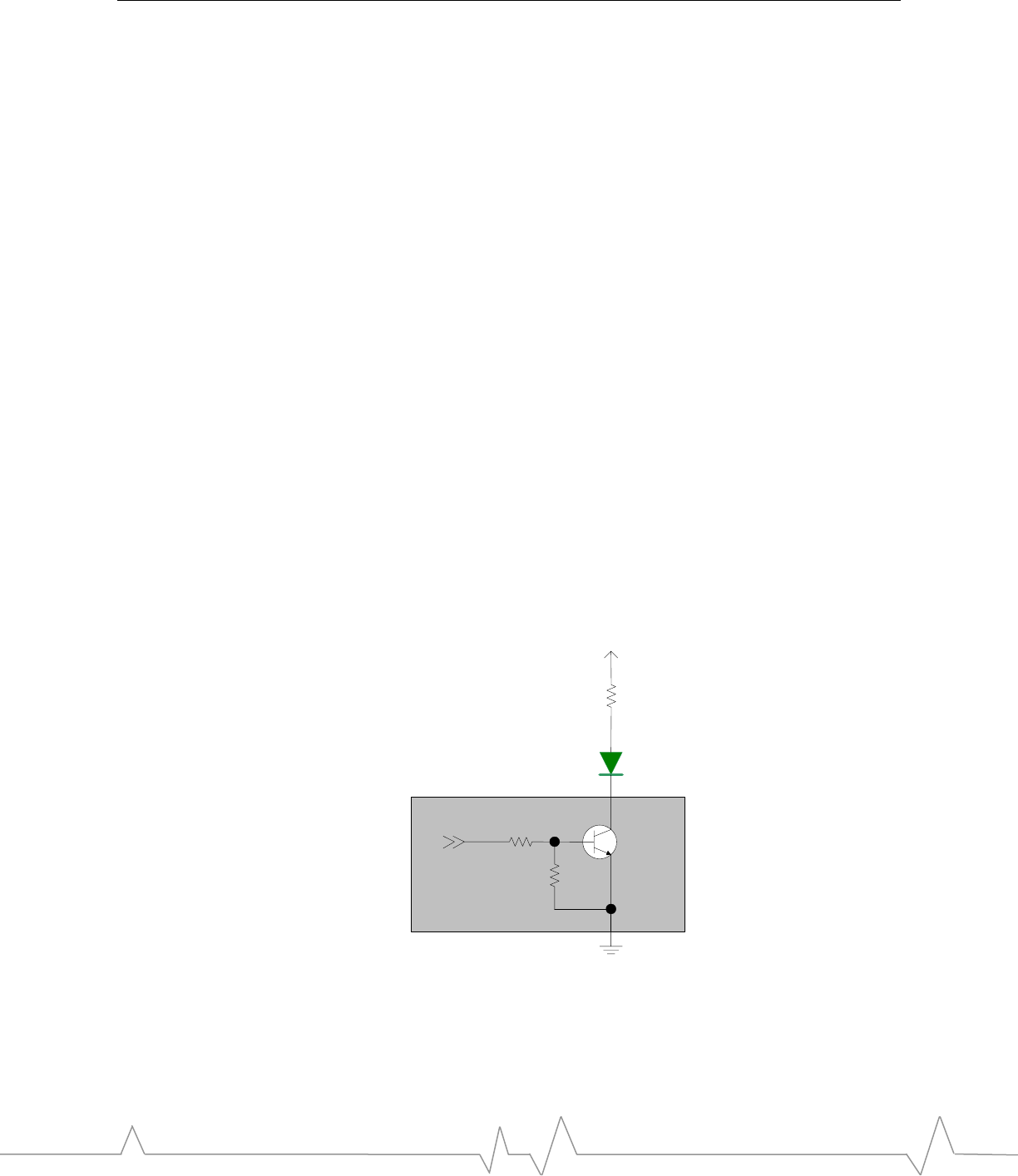
LED output
The MiniCard Drives the LED output according to the PCI-Express MiniCard
specification.
Figure 9: Example LED
Current limiting Resistor
LED
VCC 3.3V
MIO
MiniCard
PCI Express MiniCard Hardware Integration Guide
34 Proprietary and confidential 213XXXX
XIM Interface
The EM is designed to support one SIM (Subscriber Identity Module) or RUIM
(Removable User Identity Module). SIM is a smart card developed for GSM
networks while RUIM is for CDMA cellular systems. Each provides personal
user information that allows a mobile to attach to the wireless network. The XIM
feature provides the user with handset independence.
There are four required and one optional signals in the XIM interface. These are
defined in Table 5 with an example circuit (EM3420) shown in Figure 10.
Some EM models contain the voltage regulator for the XIM interface, while
others provide an enable signal. See the EM Reference Guide for your EM
model for details.
Table 5: XIM pins
Pin name RUIM pin
number Function
XIM_VCC 1 XIM VCC
/XIM_RESET 2 Active low XIM reset
XIM_CLK 3 Serial clock for XIM data.
XIM_DATA 4 Bi-directional XIM data line
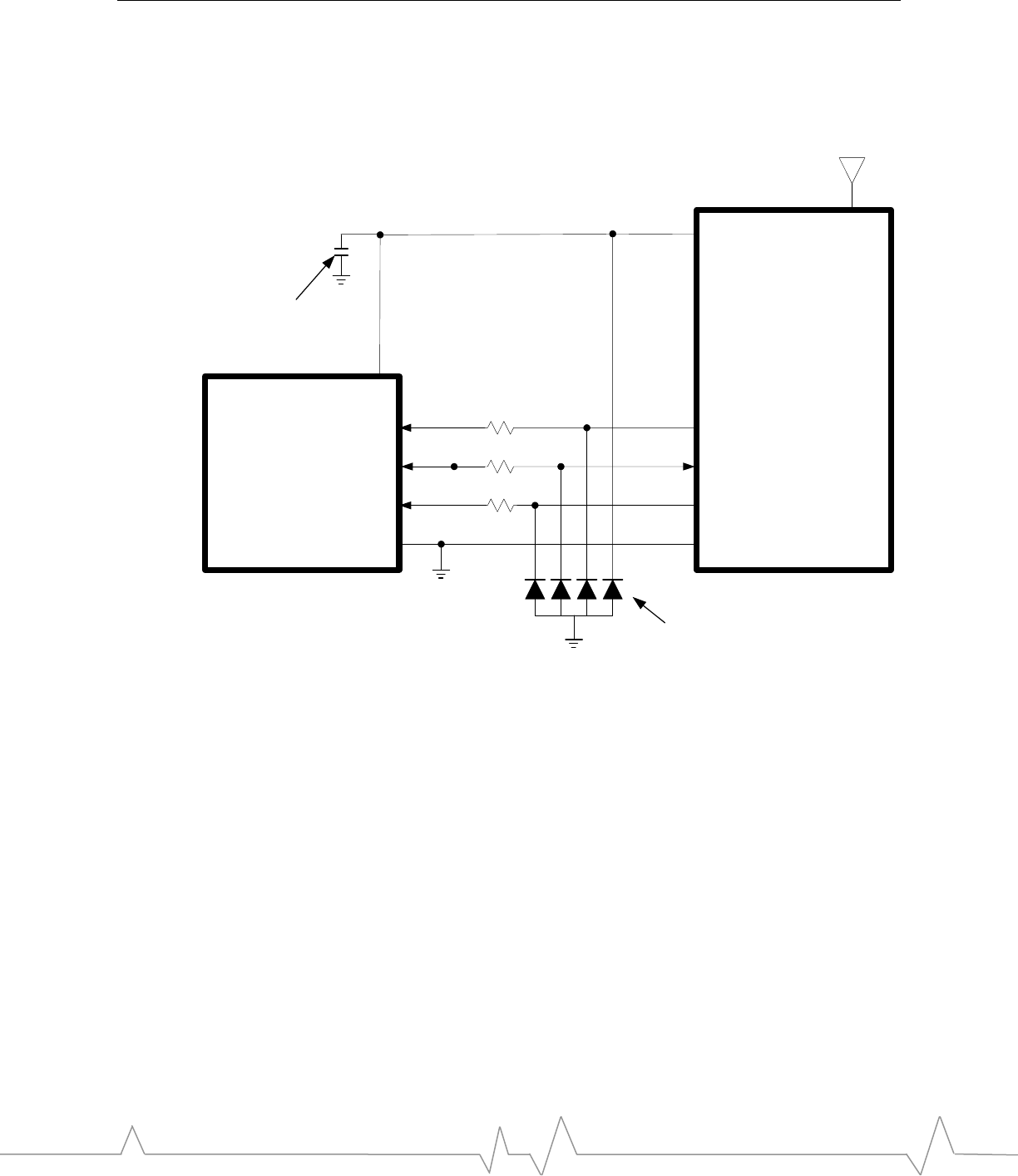
Host Interface
Rev 1.2 Apr-05 Proprietary and confidential 35
Figure 10: RUIM application interface
MCXXXX
RUIM_PWR
/RUIM_RESET
RUIM_IO
RUIM_CLK
RUIM/SIM card
connector
GND
ESD
protection
0 ohm
0 ohm
0 ohm
4.7uF
X5R
typ
pin 1
pin 3
pin 4
pin 2
pin 8
XIM_VCC
XIM_CLK
XIM_IO
/XIM_RESET
located near
SIM socket
located near
SIM socket
GND
XIM notes of operation
• To save power, the XIM interface should be powered down when not in use.
• XIM is specified to run up to 5 MHz (XIM clock rate). Take note of this
speed in the placement and routing of the XIM signals and connectors.
• To protect the modem CPU, ESD protection is required for XIM_CLK,
XIM_IO, /XIM_DETECT (if used), and /XIM_RESET lines. Additionally
spaces for possible series resistors should be added to the layout. Possible
values of up to 470 ohm may be used depending on ESD testing
requirements.
• It is recommended to put a placeholder capacitor near the SIM socket. The
longer the trace length (impedance) from the socket to the MiniCard, the
greater the capacitance requirement will be to meet compliance tests.

PCI Express MiniCard Hardware Integration Guide
36 Proprietary and confidential 213XXXX

Acronyms and definitions
Rev 1.2 Apr-05 Proprietary and confidential 37
Acronyms and definitions
Table 6: Acronyms and definitions
Acronym or term Definition
ADC Analog to Digital Converter
AGC Automatic Gain Control
Bi-directional Microphone with lower sensitivity along the circumference of the housing, higher
sensitivity towards the front and rear sections of the housing.
Call Box Base Station Simulator - Agilent E8285A or 8960, Rohde & Schwarz CMU200
Cellular 800MHz radio spectrum air interface
dB Decibel = 10 x log10 (P1/P2) (Power dB)
Decibel = 20 x log10 (V1/V2) (Voltage dB)
dBm Decibels, relative to 1 mW - Decibel(mW) = 10 x log10 (Pwr (mW)/1mW)
dBSPL Decibel unit of acoustic sound pressure - 20 x log (sound pressure in Pa / 20E-6
Pa)
dBV Decibels, relative to 1 Volt - Decibel(V) = 20 x log10 (V1/1.0V)
Directivity Sensitivity as a function of sound wave inflection angle
DUT Device Under Test
Electret Device that translates air pressure changes into electrical signals
EM Embedded Module
ESD ElectroStatic Discharge
EVRC Enhanced Variable Rate Coder – an 8kbs codec compression technique
FER Frame Error Rate – a measure of receive sensitivity
FIR Finite Impulse Response – a form of digital filter
GPIB General Purpose Interface Bus – IEEE std protocol for test equip
communication
GPS Global Positioning System
IS-95 2G radio standards targeted for voice (cdmaONE)
IS-2000 3G radio standards for voice and data-centric use
LDO Low Drop Out – refers to linear regulator
LSB Least Significant Bit
MHz MegaHertz = 1e6 Hertz (Hertz = 1/second)
MIDI Musical Instrument Digital Interface – musical note standard interface
MIO Module Input/Output
Modem Modulator – demodulator (the EM)

PCI Express MiniCard Hardware Integration Guide
38 Proprietary and confidential 213XXXX
Acronym or term Definition
MP Mass Production – the finished product.
Newton Unit of force: 1 N = force required to accelerate 1 kg object 1 meter per second
per second. F = m x a. Force = mass x acceleration
Noise-canceling Active microphone with built in filtering. Better noise cancellation performance
than Uni-directional.
Omni-directional Microphone designed to receive audio input from every direction
OTA Over the Air or Radiated through the antenna.
OVP Over Voltage Protection
Pascal Unit of pressure: 1 Pa = 1 Newton of force applied over an area of 1 meter
squared
PCS Personal Communication System - PCS spans the 1.9GHz radio spectrum
PSD Product Specification Document
QCELP Qualcomm Code Excited Linear Predicator – a 13kbs codec compression
technique
QPCH Quick Paging Channel – IS2000 feature which increases standby time when
enabled
Reverse Pilot
Gating IS2000 technique of reducing transmitter on time during conversation to
improve battery life.
RF Radio Frequency
RUIM Removable User Identity Module
Sensitivity (RF) Measure of lowest power signal that the receiver can measure
Sensitivity (Audio) Microphone performance specification – output voltage measured when the
microphone detects a given sound wave (1kHz) for fixed load conditions.
Measured in dBV/Pa.
Sidetone Feeding a fraction of transmit audio level into the receive path. This gives the
user some feedback that an audio link is established.
SIM Subscriber Identity Module
SOF Start of Frame - a USB function
UART Universal Asynchronous Receiver Transmitter
UDK Universal Development Kit
Uni-directional Microphone designed to receive audio input from a single direction. Effective in
passive reduction of background noise.
USB Universal Serial Bus
UVP Under Voltage Protection
VAF Voice Activity Factor - % time voice is active in a conversation (40% is typical).
VR Voice recognition
xIM Either RUIM or SIM, as the cards themselves are interchangeable

Acronyms and definitions
Rev 1.2 Apr-05 Proprietary and confidential 39