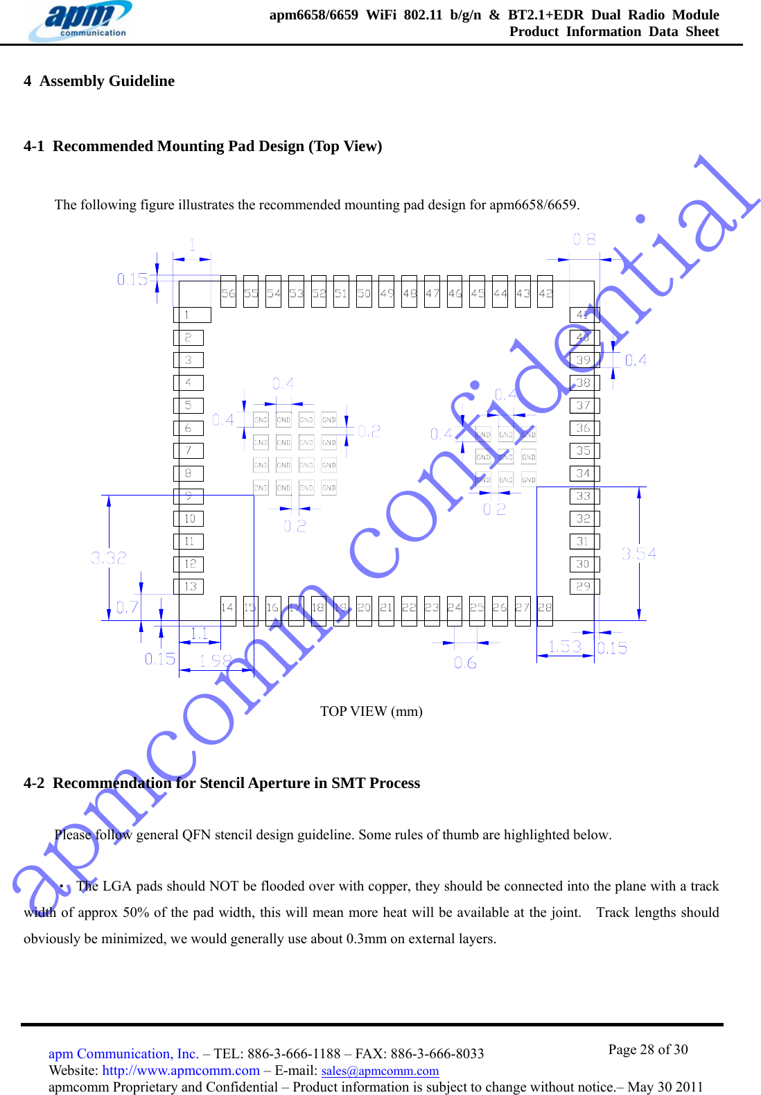
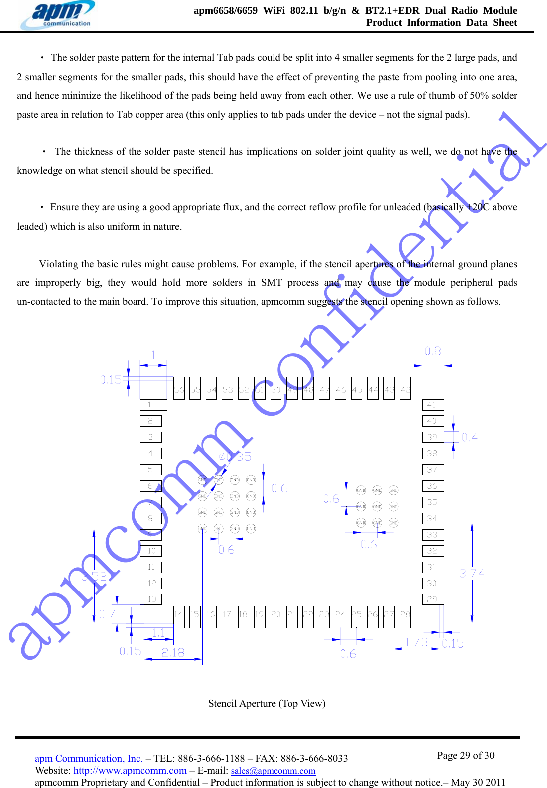
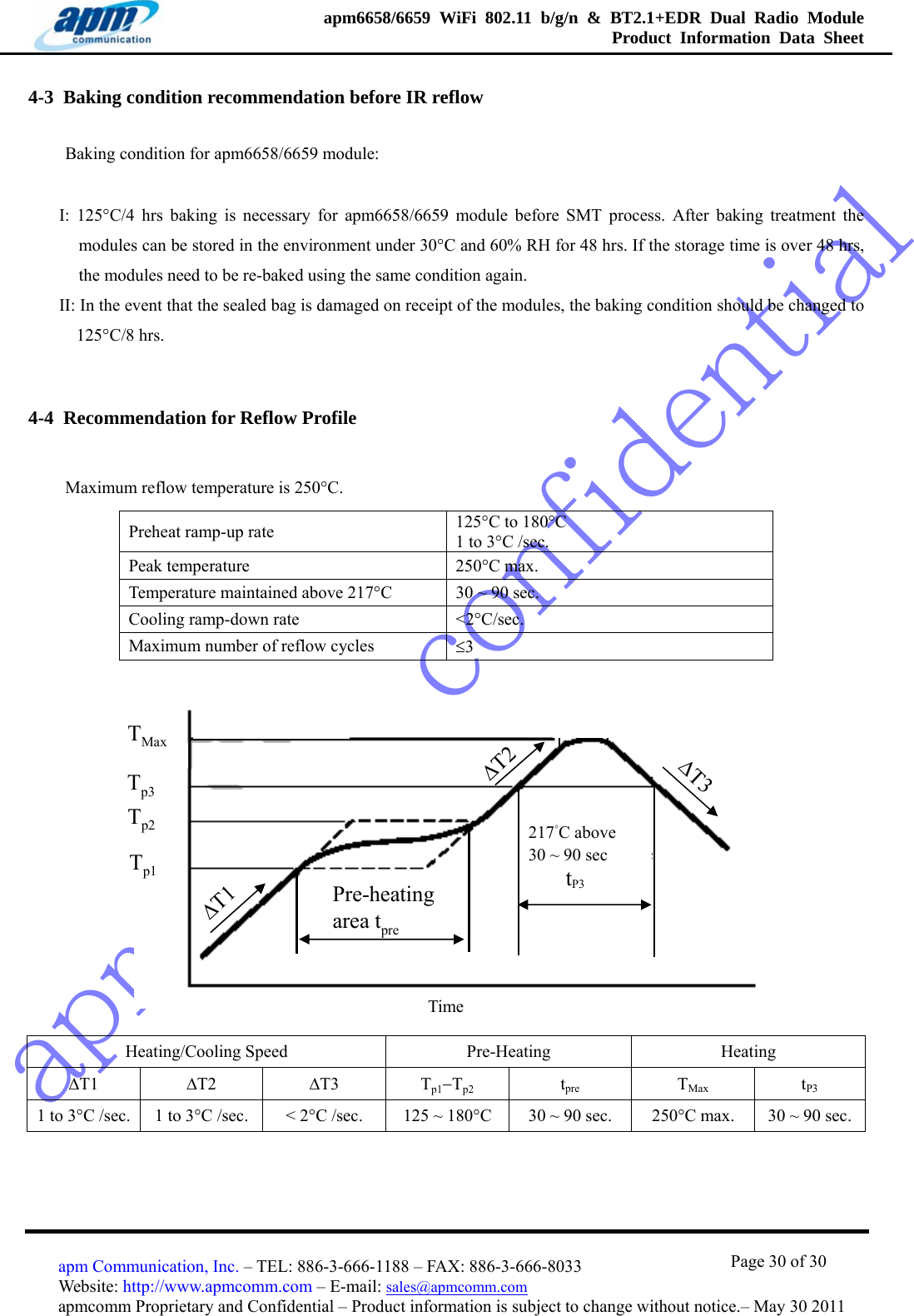
Getac Technology APM6658 BT/WLAN Module User Manual
Getac Technology Corporation BT/WLAN Module
UserManual.wiki
>
Getac Technology
>
APM6658 User Manual
User Manual
Navigation menu
Upload a User Manual
Namespaces
Wiki Guide
HTML
PDF
Info
Views
User Manual
Discussion / Help
Navigation
![apmcomm confidentialapm6658/6659 WiFi 802.11 b/g/n & BT2.1+EDR Dual Radio Module Product Information Data Sheet Page 2 of 30 apm Communication, Inc. – TEL: 886-3-666-1188 – FAX: 886-3-666-8033 Website: http://www.apmcomm.com – E-mail: sales@apmcomm.com apmcomm Proprietary and Confidential – Product information is subject to change without notice.– May 30 2011 REVISION HISTORY Date Release Author Description 1-Feb-10 0.1 Winter/Bryant Initial release 11-Jan-11 0.2 CJ Modify the 1-10 RF Specification Modify the 1-7, the 26 MHz is default setting Modify the 1-4-4, WL_PIO[9] description 30-May-11 0.3 Pol Modify the pin description in section 1-3-2 Modify recommended clock characteristics in section 1-7 Modify electrical specifications in section 1-8](https://usermanual.wiki/Getac-Technology/APM6658/User-Guide-1849791-Page-2.png)
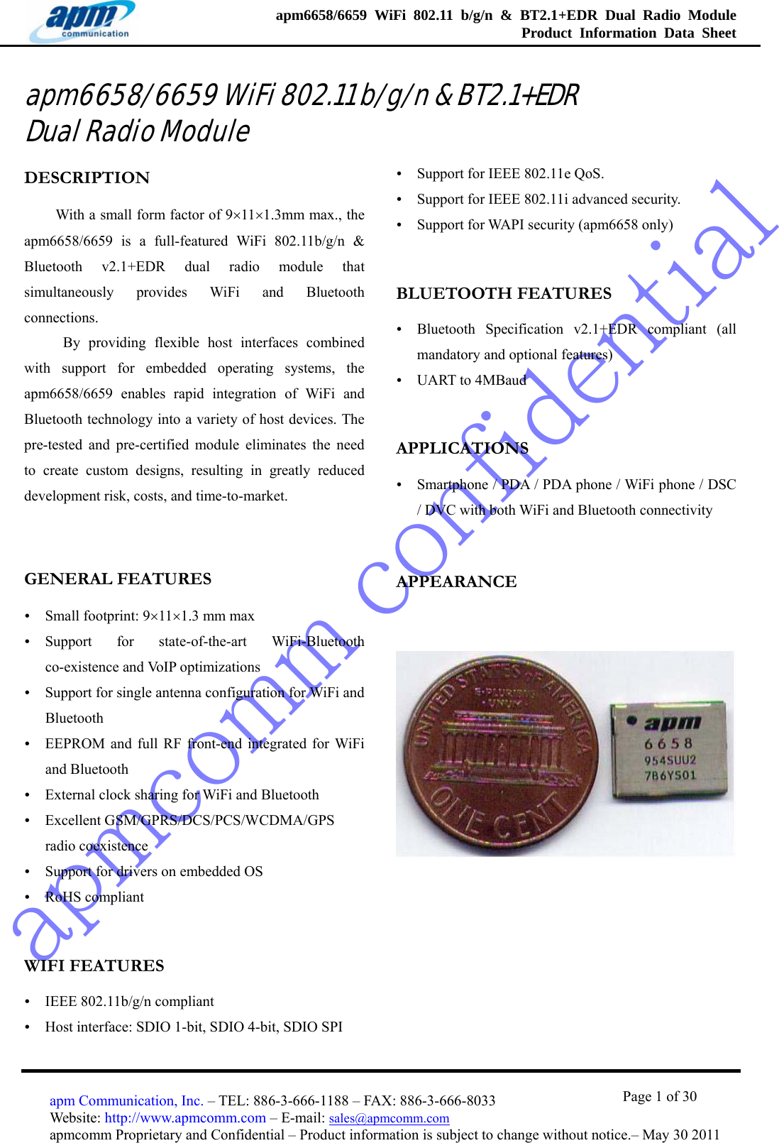
![apmcomm confidentialapm6658/6659 WiFi 802.11 b/g/n & BT2.1+EDR Dual Radio Module Product Information Data Sheet Page 7 of 30 apm Communication, Inc. – TEL: 886-3-666-1188 – FAX: 886-3-666-8033 Website: http://www.apmcomm.com – E-mail: sales@apmcomm.com apmcomm Proprietary and Confidential – Product information is subject to change without notice.– May 30 2011 1-3 Pinout 1-3-1 Pin Assignment BT_SPI_CSB 51WL_VSDIO23BT_PCM_CLK 55WL_PIO[12] 31GND 41WL_SPI_MOSI5WL_SD_DAT[0] 29BT_UART_CTS10GND 43WL_PIO[9]9WL_PIO[11] 34WL_1V819BT_UART_RX15BT_SD_CMD12BT_SPI_MOSI 50GND 35WL_SPI_MISO3BT_UART_TX14Ant 53BT_CLK7BT_PCM_OUT2BT_SPI_CLK 45WL_RESETn 30WL_SPI_CSn6WL_SD_CMD28WL_SD_CLK25WL_SD_DAT[2]24BT_PIO[0] 36WL_PIO[10] 33WL_SPI_CLK4BT_PIO[4]20WL_VDD_PADS_0_7 47BT_PCM_IN1BT_SD_CLK11WL_SD_DAT[3]26BT_UART_RTS16BT_EN 39WL_WP 40GND 52BT_PIO[2]22apm6658/6659BT_PCM_SYNC 56BT_VDD_PADS18BT_RESETB 32WL_VREG_EN21GND 54BT_PIO[3] 37BT_CLK32K17BT_SPI_MISO 46WL_SD_DAT[1]27BT_VREGL 49BT_VREGH 48WL_CLK8WL_VDD3V3 38BT_SD_CSn13GND 42GND 44](https://usermanual.wiki/Getac-Technology/APM6658/User-Guide-1849791-Page-7.png)
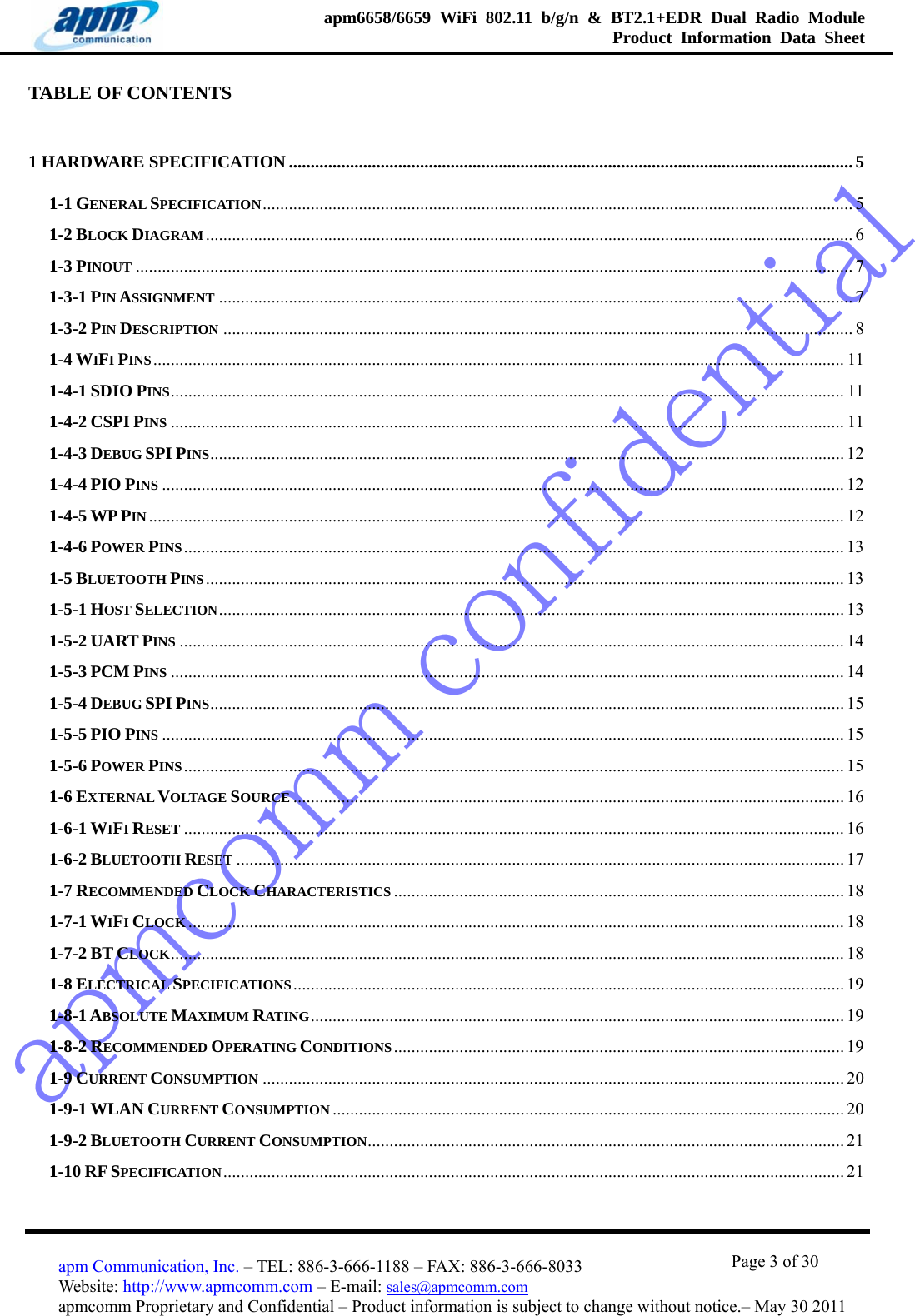
![apmcomm confidentialapm6658/6659 WiFi 802.11 b/g/n & BT2.1+EDR Dual Radio Module Product Information Data Sheet Page 8 of 30 apm Communication, Inc. – TEL: 886-3-666-1188 – FAX: 886-3-666-8033 Website: http://www.apmcomm.com – E-mail: sales@apmcomm.com apmcomm Proprietary and Confidential – Product information is subject to change without notice.– May 30 2011 1-3-2 Pin Description * I/O: Digital Input/Output, I: Digital Input, O: Digital Output, A: Analog, PU: Pull-up, PD: Pull-down # Name I/O Pin Status on Reset Supply Domain Description 1 BT_PCM_IN I PD BT_VDD_PADS Synchronous data input 2 BT_PCM_OUT O PD BT_VDD_PADS Synchronous data output 3 WL_SPI_MISO O PD WL_VDD_PADS_0_7 Debug SPI data output 4 WL_SPI_CLK I PD WL_VDD_PADS_0_7 Debug SPI clock 5 WL_SPI_MOSI I PD WL_VDD_PADS_0_7 Debug SPI data input 6 WL_SPI_CSn I PU WL_VDD_PADS_0_7 Debug SPI chip select, active low 7 BT_CLK I - - Clock input for BT 8 WL_CLK I - - Clock input for WiFi 9 WL_PIO[9] I/O PD WL_3V3 Programmable input/output 10 BT_UART_CTS I/O PU BT_VDD_PADS UART clear to send, active low 11 BT_SD_CLK I PU BT_VDD_PADS SDIO Clock 12 BT_SD_CMD I PU BT_VDD_PADS SDIO data input 13 BT_SD_CSn I PU BT_VDD_PADS SDIO chip select to allow SDIO accesses 14 BT_UART_TX O PU BT_VDD_PADS UART data output active high 15 BT_UART_RX I PU BT_VDD_PADS UART data input active high 16 BT_UART_RTS O PU BT_VDD_PADS UART request to send active low 17 BT_CLK32K I PD BT_VDD_PADS Dedicated 32kHz external reference clock input 18 BT_VDD_PADS Power - - Positive supply for all digital Input/Output ports, UART/SDIO ports, and PIO ports 19 WL_1V8 Power - - Power supply for analogue/digital sections 20 BT_PIO[4] I/O PD BT_VDD_PADS Programmable input/output 21 WL_VREG_EN Power PD - Take high to enable regulator 22 BT_PIO[2] I/O PD BT_VDD_PADS Programmable input/output 23 WL_VSDIO Power - - Host interface digital I/O power supply 24 WL_SD_DAT[2] I/O PU WL_VSDIO SDIO 4-bit mode: Data line [bit 2] or Read wait (optional) SDIO 1-bit mode: Read Wait(optional) SDIO SPI mode: Reserved](https://usermanual.wiki/Getac-Technology/APM6658/User-Guide-1849791-Page-8.png)
![apmcomm confidentialapm6658/6659 WiFi 802.11 b/g/n & BT2.1+EDR Dual Radio Module Product Information Data Sheet Page 9 of 30 apm Communication, Inc. – TEL: 886-3-666-1188 – FAX: 886-3-666-8033 Website: http://www.apmcomm.com – E-mail: sales@apmcomm.com apmcomm Proprietary and Confidential – Product information is subject to change without notice.– May 30 2011 # Name I/O Pin Status on Reset Supply Domain Description 25 WL_SD_CLK I PU WL_VSDIO SDIO 4-bit mode: Clock SDIO 1-bit mode: Clock CSPI mode : Clock 26 WL_SD_DAT[3] I/O PU WL_VSDIO SDIO 4-bit mode: Data line [bit 3] SDIO 1-bit mode: Reserved CSPI mode: Card Select 27 WL_SD_DAT[1] I/O PU WL_VSDIO SDIO 4-bit mode: Data line [bit 1] or interrupt SDIO 1-bit mode: Interrupt CSPI mode : Intrrupt 28 WL_SD_CMD I PU WL_VSDIO SDIO 4-bit mode: Command/Response SDIO 1-bit mode: Command/Response CSPI mode: Data input 29 WL_SD_DAT[0] I/O PU WL_VSDIO LSB data bit for SDIO interface. SDIO 4-bit mode: Data line [bit 0] SDIO 1-bit mode: Data line CSPI mode: Data output 30 WL_RESETn I PU WL_RESETB Reset, active low 31 WL_PIO[12] I/O PD WL_3V3 Programmable input/output 32 BT_RESETB I PU BT_VDD_PADS Reset if low. Input debounced so must be low for >5ms to cause a reset. 33 WL_PIO[10] I/O PD WL_3V3 Programmable input/output 34 WL_PIO[11] I/O PD WL_3V3 Programmable input/output 35 GND GND - - Ground 36 BT_PIO[0] I/O PD BT_VDD_PADS Programmable input/output 37 BT_PIO[3] I/O PD BT_VDD_PADS Programmable input/output 38 WL_3V3 Power - - Positive supply for AIO[0]-AIO[3] , PIO[8]-PIO[15], and FEM 39 BT_EN I - - Take high to enable regulator 40 WL_WP I - - Write protection for internal EEPROM 41 GND GND - - Ground 42 GND GND - - Ground 43 GND GND - - Ground 44 GND GND - - Ground 45 BT_SPI_CLK I PD BT_VDD_PADS Serial Peripheral Interface clock](https://usermanual.wiki/Getac-Technology/APM6658/User-Guide-1849791-Page-9.png)
![apmcomm confidentialapm6658/6659 WiFi 802.11 b/g/n & BT2.1+EDR Dual Radio Module Product Information Data Sheet Page 10 of 30 apm Communication, Inc. – TEL: 886-3-666-1188 – FAX: 886-3-666-8033 Website: http://www.apmcomm.com – E-mail: sales@apmcomm.com apmcomm Proprietary and Confidential – Product information is subject to change without notice.– May 30 2011 # Name I/O Pin Status on Reset Supply Domain Description 46 BT_SPI_MISO O PD BT_VDD_PADS Serial Peripheral Interface data output47 WL_VDD_PADS_0_7 Power - - Positive supply for Debug SPI, PIO[0]-PIO[7] 48 BT_VREGH Power - - High regulator input 49 BT_VREGL Power - - High regulator output and low regulator input 50 BT_SPI_MOSI I PD BT_VDD_PADS Serial Peripheral Interface data input51 BT_SPI_CSB I PU BT_VDD_PADS Chip select for Serial Peripheral Interface, active low 52 GND GND - - Ground 53 ANT A - - RF input/output 54 GND GND - - Ground 55 BT_PCM_CLK I/O PD BT_VDD_PADS Synchronous data clock 56 BT_PCM_SYNC I/O PD BT_VDD_PADS Synchronous data sync All the big pads on the bottom of the module should be tied to ground.](https://usermanual.wiki/Getac-Technology/APM6658/User-Guide-1849791-Page-10.png)
![apmcomm confidentialapm6658/6659 WiFi 802.11 b/g/n & BT2.1+EDR Dual Radio Module Product Information Data Sheet Page 11 of 30 apm Communication, Inc. – TEL: 886-3-666-1188 – FAX: 886-3-666-8033 Website: http://www.apmcomm.com – E-mail: sales@apmcomm.com apmcomm Proprietary and Confidential – Product information is subject to change without notice.– May 30 2011 1-4 WiFi Pins 1-4-1 SDIO Pins apm6658/6659 supports a SDIO device interface that conforms to the industry standard SDIO Full-Speed card specification and allows a host controller using the SDIO bus protocol to access apm6658/6659. The SDIO bus has weak internal pull up resistors on chip. SDIO Bus Name Pin # Pin Name Description DAT3 26 WL_SD_DAT[3] SDIO 4-bit mode: CD- Data line [bit 3] or card detect SDIO 1-bit mode: CD- Card detect DAT2 24 WL_SD_DAT[2] SDIO 4-bit mode: RW- Data line [bit 2] or read wait(optional) SDIO 1-bit mode: RW- Read Wait (optional) DAT1 27 WL_SD_DAT[1] SDIO 4-bit mode: IRQ#- Data line [bit 1] or interrupt (optional) SDIO 1-bit mode: IRQ#- Interrupt DAT0 29 WL_SD_DAT[0]LSB data bit for SDIO interface. SDIO 4-bit mode: Data line [bit 0] SDIO 1-bit mode: Data line CMD 28 WL_SD_CMD SDIO 4-bit mode: Command/Response SDIO 1-bit mode: Command/Response CLK 25 WL_SD_CLK SDIO 4-bit mode: Clock SDIO 1-bit mode: Clock VDDIO 23 WL_VSDIO Serial I/O VDD 1-4-2 CSPI Pins While SDIO port is not available on host platform, apm6658/6659 supports a SD-SPI device interface that connects to Synchronous Serial Port (SSP) pins on Marvell PXA platform or the similar interfaces on other host platforms. The SD-SPI bus has weak internal pull up resistors on chip. SD-SPI Name Pin # Pin Name Description CS 26 WL_SD_DAT[3] Card Select](https://usermanual.wiki/Getac-Technology/APM6658/User-Guide-1849791-Page-11.png)
![apmcomm confidentialapm6658/6659 WiFi 802.11 b/g/n & BT2.1+EDR Dual Radio Module Product Information Data Sheet Page 12 of 30 apm Communication, Inc. – TEL: 886-3-666-1188 – FAX: 886-3-666-8033 Website: http://www.apmcomm.com – E-mail: sales@apmcomm.com apmcomm Proprietary and Confidential – Product information is subject to change without notice.– May 30 2011 SD-SPI Name Pin # Pin Name Description IRQ 27 WL_SD_DAT[1] Interrupt DO 29 WL_SD_DAT[0] Data output DI 28 WL_SD_CMD Data input SCLK 25 WL_SD_CLK Clock VDDIO 23 WL_VSDIO Serial I/O VDD 1-4-3 Debug SPI Pins apm6658/6659 has a SPI interface for test and debugging purposes. The lab tools, such as UniTest and UniPSUtil, can communicate with apm6658/6659 WiFi part using the SPI protocol over a connection to an LPT port. Debug SPI Name Pin # Pin Name Description MISO 3 WL_SPI_MISO Debug SPI data output MOSI 5 WL_SPI_MOSI Debug SPI data input CLK 4 WL_SPI_CLK Debug SPI clock CSn 6 WL_SPI_CSn Debug SPI chip select, active low VDDIO 47 WL_VPADS_0_7 Serial I/O VDD 1-4-4 PIO Pins The PIO pins are used to implement user defined input and output signals to and from the module such as external interrupts, LED controlled outputs, and other user-defined I/Os. Each PIO can be independently controlled. z WL_PIO[11:10]: LED WLAN link activities. z WL_PIO[12]: Host wakeup. z WL_PIO[9]: WiFi External clock request out z Other PIOs: Reserved 1-4-5 WP Pin WL_WP is write protection for internal EEPROM. The internal EEPROM stores calibration table, MAC address, etc. for WiFi part. When the pin is pulled high, it protects the EEPROM content. If tied to VSS, normal memory read/write operation is enabled.](https://usermanual.wiki/Getac-Technology/APM6658/User-Guide-1849791-Page-12.png)
![apmcomm confidentialapm6658/6659 WiFi 802.11 b/g/n & BT2.1+EDR Dual Radio Module Product Information Data Sheet Page 13 of 30 apm Communication, Inc. – TEL: 886-3-666-1188 – FAX: 886-3-666-8033 Website: http://www.apmcomm.com – E-mail: sales@apmcomm.com apmcomm Proprietary and Confidential – Product information is subject to change without notice.– May 30 2011 The WiFi firmware does not incorporate any support for writing to the EEPROM during normal operation. This significantly reduces the risk of spurious writes corrupting the contents of the EEPROM, and means it is not possible to repair any damage that may occur. Hence, it is suggested that keep the pin, WL_WP, permanently pulled high to minimize the risk of data corruption. 1-4-6 Power Pins The following list shows the pins referenced to WL_VSDIO. Pin # Pin name Pin # Pin name Pin # Pin name 24 WL_SD_DAT[2] 25 WL_SD_CLK 26 WL_SD_DAT[3] 27 WL_SD_DAT[1] 28 WL_SD_CMD 29 WL_SD_DAT[0] The following list shows the pins referenced to WL_VDD_PADS_0_7. Pin # Pin name Pin # Pin name Pin # Pin name 3 WL_SPI_MISO 4 WL_SPI_CLK 5 WL_SPI_MOSI 6 WL_SPI_CSn 30 WL_RESETn The following list shows the pins referenced to WL_3V3. Pin # Pin name Pin # Pin name Pin # Pin name 9 WL_PIO[9] 33 WL_PIO[10] 34 WL_PIO[11] 31 WL_PIO[12] *WL_VDD_PADS_0_7 voltage power level must be the same as BT_VDD_PADS and the oscillator. 1-5 Bluetooth Pins 1-5-1 Host Selection The apm6658/6659 selects the UART interface by reading BT_PIO[4] at boot-time. When BT_PIO[4] is low, the UART is enabled.](https://usermanual.wiki/Getac-Technology/APM6658/User-Guide-1849791-Page-13.png)
![apmcomm confidentialapm6658/6659 WiFi 802.11 b/g/n & BT2.1+EDR Dual Radio Module Product Information Data Sheet Page 15 of 30 apm Communication, Inc. – TEL: 886-3-666-1188 – FAX: 886-3-666-8033 Website: http://www.apmcomm.com – E-mail: sales@apmcomm.com apmcomm Proprietary and Confidential – Product information is subject to change without notice.– May 30 2011 1-5-4 Debug SPI Pins apm6658/6659 has a SPI interface for debug primarily. The lab tools, PSTOOL, can communicate with apm6658/6659 BT part using the SPI protocol over a connection to an LPT port. Debug SPI Name Pin # Pin Name Description MISO 46 BT_SPI_MISO Debug SPI data output MOSI 50 BT_SPI_MOSI Debug SPI data input CLK 45 BT_SPI_CLK Debug SPI clock CS 51 BT_SPI_CS Debug SPI chip select, active low VDDIO 18 BT_VDD_PADS Serial I/O VDD 1-5-5 PIO Pins The PIO pins are used to implement user defined input and output signals to and from the module such as external interrupts, LED controlled output and other user-defined I/Os. Each PIO can be independently controlled. z BT_PIO[0]: LED Bluetooth RX activities z BT_PIO[2]: Bluetooth external clock request out z BT_PIO[3]: Bluetooth external clock request in. z BT_PIO[4]: The module selects the UART interface by reading BT_PIO[4] at boot-time. When BT_PIO[4] is low, the UART interface is enabled. 1-5-6 Power Pins The following list shows the pins referenced to BT_VDD_PADS. Pin # Pin name Pin # Pin name Pin # Pin name 1 BT_PCM_IN 16 BT_UART_RTS 46 BT_SPI_MISO 2 BT_PCM_OUT 17 BT_CLK32K 50 BT_SPI_MOSI 10 BT_UART_CTS 20 BT_PIO[4] 51 BT_SPI_CSB 11 BT_SD_CLK 22 BT_PIO[2] 55 BT_PCM_CLK 12 BT_SD_CMD 32 BT_RESETB 56 BT_PCM_SYNC](https://usermanual.wiki/Getac-Technology/APM6658/User-Guide-1849791-Page-15.png)
![apmcomm confidentialapm6658/6659 WiFi 802.11 b/g/n & BT2.1+EDR Dual Radio Module Product Information Data Sheet Page 16 of 30 apm Communication, Inc. – TEL: 886-3-666-1188 – FAX: 886-3-666-8033 Website: http://www.apmcomm.com – E-mail: sales@apmcomm.com apmcomm Proprietary and Confidential – Product information is subject to change without notice.– May 30 2011 Pin # Pin name Pin # Pin name Pin # Pin name 13 BT_SD_CS 36 BT_PIO[0] 14 BT_UART_TX 37 BT_PIO[3] 15 BT_UART_RX 45 BT_SPI_CLK *BT_VDD_PADS voltage power level must be the same as WL_VDD_PADS_0_7 1-6 External Voltage Source The external supply rails to apm6658/6659 should have less than 10mV rms noise levels between 0 to 10 MHz. Single tone frequencies are also to be avoided. Transient response of external regulators used should be <= 5us for WiFi and <= 20us for Bluetooth, respectively. Supply voltage range 1.8V 1.8V+/- 5% (ripple Vpp<10mV rms) 3.3V 3.3V +/-5% (ripple Vpp<10mV rms) 1-6-1 WiFi Reset WL_RESETn is an active low reset input that is internally filtered using the internal low frequency clock oscillator to avoid spurious resets. A reset occurs after the signal has been asserted for between 250 and 375us. This pin may be tied to WL_VDD_PADS_0_7 if unused; otherwise it should be asserted for at least 1ms to force a reset. The power supply supervisor monitors WL_VDD_CORE (internal module voltage) to trigger a power-on-reset. This occurs when the supply falls below 1.05V (typical) in normal operation or 0.825V (typical) in deep sleep, and ends when the supply exceeds 1.10V (typical). Glitches of up to 30mV and 2.5us duration, which could be caused by large load steps, will not trigger a reset. Each of the internal processors has its own independent watchdog timer to detect and recover from erroneous software operation. These are typically configured with a timeout of 1.5s, but this may be increased up to a maximum of 64s for reduced power consumption. The watchdogs are enabled at power-on and continue operating while WiFi is in deep sleep. During all forms of reset most digital I/O pins (including both bidirectional pins and dedicated inputs or outputs) default to high impedance with weak internal pull-downs. The only exceptions are WL_RESETn and WL_SPI_CS which both have pull-ups, and the SDIO/CSPI bus which is on an independent reset domain. The SDIO/CSPI host interface is only fully reset by the WL_RESETn pin or the power supply supervisor; other forms of reset leave the host interface initialized but simply clear the I/O Enable bit for function 1. Following a reset, WiFi automatically generates safe clocks for internal use. If an external reference clock is connected to WL_CLK then this is assumed to be at the maximum supported frequency, otherwise the PLL free runs at](https://usermanual.wiki/Getac-Technology/APM6658/User-Guide-1849791-Page-16.png)
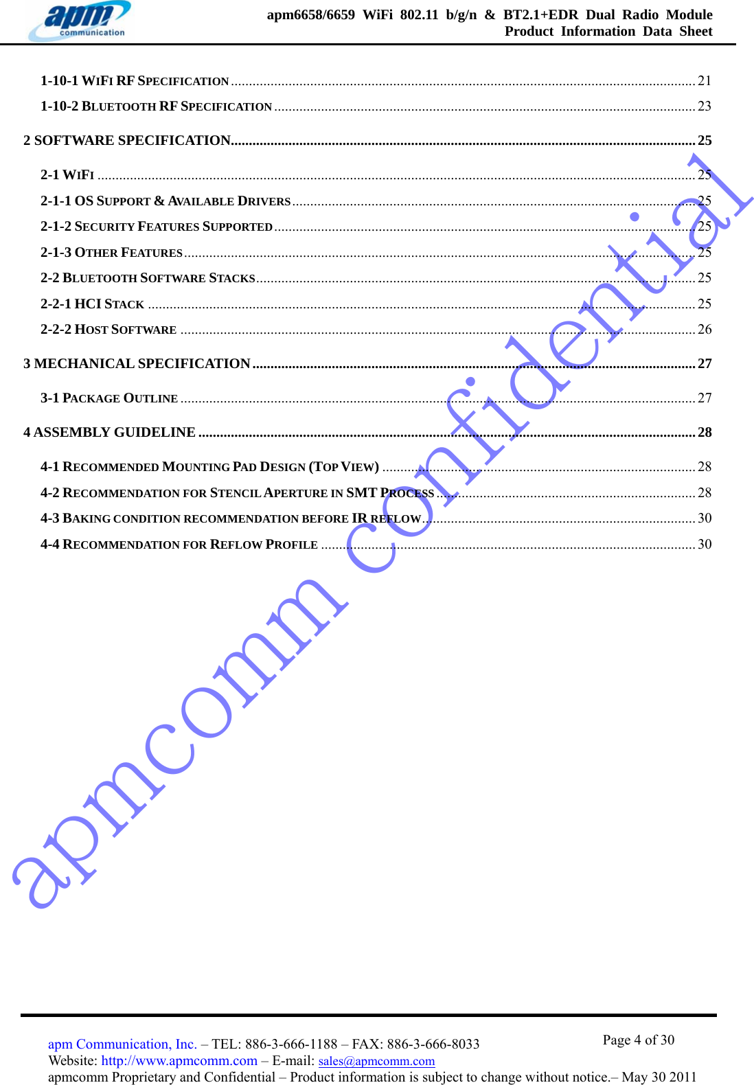
![apmcomm confidentialapm6658/6659 WiFi 802.11 b/g/n & BT2.1+EDR Dual Radio Module Product Information Data Sheet Page 19 of 30 apm Communication, Inc. – TEL: 886-3-666-1188 – FAX: 886-3-666-8033 Website: http://www.apmcomm.com – E-mail: sales@apmcomm.com apmcomm Proprietary and Confidential – Product information is subject to change without notice.– May 30 2011 1-8 Electrical Specifications 1-8-1 Absolute Maximum Rating Symbol Description Min. Max. Units TST Storage temperature -30 +85 °C WL_3V3 Positive supply for AIO[0]-AIO[3] , PIO[8]-PIO[15], and FEM +1.7 +3.6 V WL_1V8 Power supply for VDD_REG_IN_ANA, VDD_REG_IN_DIG. -0.3 +2.0 V WL_VREG_EN Enable for WiFi linear regulators -0.4 +2.5 V WL_VDD_PADS_0_7 Power supply for SPI, EEPROM, RST#, EEPROM and PIO[0]-PIO[7] +1.7 +3.6 V WL_VSDIO Positive supply for SDIO interface +1.7 +3.6 V BT_VREGH High regulator input -0.4 +4.9 V BT_VREGL High regulator output and low regulator input -0.4 +2.7 V BT_VDD_PADS Positive supply for digital input/output ports -0.4 +3.7 V BT_EN Take high to enable BT regulator -0.4 +4.9 V *Absolute maximum ratings indicate limits beyond which damage to the device may occur. 1-8-2 Recommended Operating Conditions Symbol Description Min. Typ. Max. UnitsTOP Operating temperature -20 +25 +70 °C WL_3V3 Positive supply for AIO[0]-AIO[3] , PIO[8]-PIO[15], and FEM +2.7 +3.3 +3.3 V WL_1V8 Power supply for VDD_REG_IN_ANA, VDD_REG_IN_DIG. +1.45 +1.8 +2.0 V WL_VREG_EN Enable for WiFi voltage regulators +1.45 +1.8 +2.0 V WL_VDD_PADS_0_7 Power supply for SPI, RST#, and PIO[0]-PIO[7] +1.7 +1.8/+3.3 +3.3 V WL_VSDIO Positive supply for SDIO interface +1.7 +1.8/+3.3 +3.6 V BT_VREGH High regulator input +2.7 +3.3 +4.9 V BT_VREGL High regulator output and low regulator input +1.7 +1.8 +2.7 V BT_VDD_PADS Positive supply for digital I/O ports +1.7 +1.8/+3.3 +3.7 V BT_EN Take high to enable BT regulator +1.7 +3.3 +3.6 V](https://usermanual.wiki/Getac-Technology/APM6658/User-Guide-1849791-Page-19.png)