Getac Technology APM6658 BT/WLAN Module User Manual
Getac Technology Corporation BT/WLAN Module
User Manual
apmcomm confidential
apm6658/6659 WiFi 802.11 b/g/n & BT2.1+EDR Dual Radio Module
Product Information Data Sheet
Page 1 of 30
apm Communication, Inc. – TEL: 886-3-666-1188 – FAX: 886-3-666-8033
Website: http://www.apmcomm.com – E-mail: sales@apmcomm.com
apmcomm Proprietary and Confidential – Product information is subject to change without notice.– May 30 2011
apm6658/6659 WiFi 802.11 b/g/n & BT2.1+EDR
Dual Radio Module
DESCRIPTION
With a small form factor of 9×11×1.3mm max., the
apm6658/6659 is a full-featured WiFi 802.11b/g/n &
Bluetooth v2.1+EDR dual radio module that
simultaneously provides WiFi and Bluetooth
connections.
By providing flexible host interfaces combined
with support for embedded operating systems, the
apm6658/6659 enables rapid integration of WiFi and
Bluetooth technology into a variety of host devices. The
pre-tested and pre-certified module eliminates the need
to create custom designs, resulting in greatly reduced
development risk, costs, and time-to-market.
GENERAL FEATURES
y Small footprint: 9×11×1.3 mm max
y Support for state-of-the-art WiFi-Bluetooth
co-existence and VoIP optimizations
y Support for single antenna configuration for WiFi and
Bluetooth
y EEPROM and full RF front-end integrated for WiFi
and Bluetooth
y External clock sharing for WiFi and Bluetooth
y Excellent GSM/GPRS/DCS/PCS/WCDMA/GPS
radio coexistence
y Support for drivers on embedded OS
y RoHS compliant
WIFI FEATURES
y IEEE 802.11b/g/n compliant
y Host interface: SDIO 1-bit, SDIO 4-bit, SDIO SPI
y Support for IEEE 802.11e QoS.
y Support for IEEE 802.11i advanced security.
y Support for WAPI security (apm6658 only)
BLUETOOTH FEATURES
y Bluetooth Specification v2.1+EDR compliant (all
mandatory and optional features)
y UART to 4MBaud
APPLICATIONS
y Smartphone / PDA / PDA phone / WiFi phone / DSC
/ DVC with both WiFi and Bluetooth connectivity
APPEARANCE

apmcomm confidential
apm6658/6659 WiFi 802.11 b/g/n & BT2.1+EDR Dual Radio Module
Product Information Data Sheet
Page 2 of 30
apm Communication, Inc. – TEL: 886-3-666-1188 – FAX: 886-3-666-8033
Website: http://www.apmcomm.com – E-mail: sales@apmcomm.com
apmcomm Proprietary and Confidential – Product information is subject to change without notice.– May 30 2011
REVISION HISTORY
Date Release Author Description
1-Feb-10 0.1 Winter/Bryant Initial release
11-Jan-11 0.2 CJ
Modify the 1-10 RF Specification
Modify the 1-7, the 26 MHz is default setting
Modify the 1-4-4, WL_PIO[9] description
30-May-11 0.3 Pol
Modify the pin description in section 1-3-2
Modify recommended clock characteristics in section
1-7
Modify electrical specifications in section 1-8

apmcomm confidential
apm6658/6659 WiFi 802.11 b/g/n & BT2.1+EDR Dual Radio Module
Product Information Data Sheet
Page 3 of 30
apm Communication, Inc. – TEL: 886-3-666-1188 – FAX: 886-3-666-8033
Website: http://www.apmcomm.com – E-mail: sales@apmcomm.com
apmcomm Proprietary and Confidential – Product information is subject to change without notice.– May 30 2011
TABLE OF CONTENTS
1 HARDWARE SPECIFICATION .................................................................................................................................5
1-1 GENERAL SPECIFICATION....................................................................................................................................... 5
1-2 BLOCK DIAGRAM.................................................................................................................................................... 6
1-3 PINOUT .................................................................................................................................................................... 7
1-3-1 PIN ASSIGNMENT ................................................................................................................................................. 7
1-3-2 PIN DESCRIPTION ................................................................................................................................................ 8
1-4 WIFI PINS.............................................................................................................................................................. 11
1-4-1 SDIO PINS.......................................................................................................................................................... 11
1-4-2 CSPI PINS .......................................................................................................................................................... 11
1-4-3 DEBUG SPI PINS................................................................................................................................................. 12
1-4-4 PIO PINS ............................................................................................................................................................ 12
1-4-5 WP PIN............................................................................................................................................................... 12
1-4-6 POWER PINS....................................................................................................................................................... 13
1-5 BLUETOOTH PINS.................................................................................................................................................. 13
1-5-1 HOST SELECTION............................................................................................................................................... 13
1-5-2 UART PINS ........................................................................................................................................................ 14
1-5-3 PCM PINS .......................................................................................................................................................... 14
1-5-4 DEBUG SPI PINS................................................................................................................................................. 15
1-5-5 PIO PINS ............................................................................................................................................................ 15
1-5-6 POWER PINS....................................................................................................................................................... 15
1-6 EXTERNAL VOLTAGE SOURCE .............................................................................................................................. 16
1-6-1 WIFI RESET ....................................................................................................................................................... 16
1-6-2 BLUETOOTH RESET ........................................................................................................................................... 17
1-7 RECOMMENDED CLOCK CHARACTERISTICS ....................................................................................................... 18
1-7-1 WIFI CLOCK ...................................................................................................................................................... 18
1-7-2 BT CLOCK.......................................................................................................................................................... 18
1-8 ELECTRICAL SPECIFICATIONS.............................................................................................................................. 19
1-8-1 ABSOLUTE MAXIMUM RATING.......................................................................................................................... 19
1-8-2 RECOMMENDED OPERATING CONDITIONS....................................................................................................... 19
1-9 CURRENT CONSUMPTION ..................................................................................................................................... 20
1-9-1 WLAN CURRENT CONSUMPTION ..................................................................................................................... 20
1-9-2 BLUETOOTH CURRENT CONSUMPTION............................................................................................................. 21
1-10 RF SPECIFICATION.............................................................................................................................................. 21

apmcomm confidential
apm6658/6659 WiFi 802.11 b/g/n & BT2.1+EDR Dual Radio Module
Product Information Data Sheet
Page 4 of 30
apm Communication, Inc. – TEL: 886-3-666-1188 – FAX: 886-3-666-8033
Website: http://www.apmcomm.com – E-mail: sales@apmcomm.com
apmcomm Proprietary and Confidential – Product information is subject to change without notice.– May 30 2011
1-10-1 WIFI RF SPECIFICATION................................................................................................................................. 21
1-10-2 BLUETOOTH RF SPECIFICATION ..................................................................................................................... 23
2 SOFTWARE SPECIFICATION.................................................................................................................................25
2-1 WIFI...................................................................................................................................................................... 25
2-1-1 OS SUPPORT & AVAILABLE DRIVERS................................................................................................................ 25
2-1-2 SECURITY FEATURES SUPPORTED..................................................................................................................... 25
2-1-3 OTHER FEATURES.............................................................................................................................................. 25
2-2 BLUETOOTH SOFTWARE STACKS.......................................................................................................................... 25
2-2-1 HCI STACK ........................................................................................................................................................ 25
2-2-2 HOST SOFTWARE ............................................................................................................................................... 26
3 MECHANICAL SPECIFICATION...........................................................................................................................27
3-1 PACKAGE OUTLINE ............................................................................................................................................... 27
4 ASSEMBLY GUIDELINE..........................................................................................................................................28
4-1 RECOMMENDED MOUNTING PAD DESIGN (TOP VIEW)....................................................................................... 28
4-2 RECOMMENDATION FOR STENCIL APERTURE IN SMT PROCESS ........................................................................ 28
4-3 BAKING CONDITION RECOMMENDATION BEFORE IR REFLOW............................................................................ 30
4-4 RECOMMENDATION FOR REFLOW PROFILE ........................................................................................................ 30

apmcomm confidential
apm6658/6659 WiFi 802.11 b/g/n & BT2.1+EDR Dual Radio Module
Product Information Data Sheet
Page 5 of 30
apm Communication, Inc. – TEL: 886-3-666-1188 – FAX: 886-3-666-8033
Website: http://www.apmcomm.com – E-mail: sales@apmcomm.com
apmcomm Proprietary and Confidential – Product information is subject to change without notice.– May 30 2011
1 Hardware Specification
1-1 General Specification
WiFi part:
Network Standard IEEE 802.11b/g/n Compliant
Host Interface SDIO v2.0: SDIO 1-bit, SDIO 4-bit, SDIO SPI
Frequency Band Channel 1 to 13
Data Transfer Mode OFDM & DSSS
Modulation 64QAM (MCS0-7, 400/800ns 72.2, 65, 58.5, 57.8, 52, 43.3, 39, 28.9, 26,
21.7, 19.5, 14.4, 13, 7.2, 6.5Mbps), 64QAM (54, 48Mbps), 16QAM (36,
24Mbps), QPSK (18, 12Mbps), BPSK (9, 6Mbps); CCK (11, 5.5 Mbps),
DQPSK (2 Mbps), DBPSK (1Mbps).
STBC reception for MCS0-7
Access Method Ad hoc mode, Infrastructure mode
Media Access Protocol CSMA/ CA (Carrier Sense Multiple Access with Collision Avoidance)
Antenna External single antenna support. The output impedance is 50Ω.
Bluetooth part:
Bluetooth Specification Bluetooth Specification v2.1 + EDR (all mandatory and optional features)
Interface UART, SPI and audio PCM interface
Frequency Band 2.402 to 2.480GHz (79 channels)
Modulation GFSK, π/4 DQPSK (2Mbps), and 8DPSK (3Mbps)
Antenna External single antenna support. The output impedance is 50Ω.
apmcomm confidential
apm6658/6659 WiFi 802.11 b/g/n & BT2.1+EDR Dual Radio Module
Product Information Data Sheet
Page 6 of 30
apm Communication, Inc. – TEL: 886-3-666-1188 – FAX: 886-3-666-8033
Website: http://www.apmcomm.com – E-mail: sales@apmcomm.com
apmcomm Proprietary and Confidential – Product information is subject to change without notice.– May 30 2011
1-2 Block Diagram
PIO
EEPROM
Balun
&
Matching PIO
SDIO/SDIO SPI
HCI (UART)
& audio PCM interface
3 Wire
Coexistence
BPF Debug SPI
Debug SPI
Bluetooth SOC
(ROM HCI Firmware)
Clock
FEM
WiFi SOC
(Hard MAC)
1.8V3.3V

apmcomm confidential
apm6658/6659 WiFi 802.11 b/g/n & BT2.1+EDR Dual Radio Module
Product Information Data Sheet
Page 7 of 30
apm Communication, Inc. – TEL: 886-3-666-1188 – FAX: 886-3-666-8033
Website: http://www.apmcomm.com – E-mail: sales@apmcomm.com
apmcomm Proprietary and Confidential – Product information is subject to change without notice.– May 30 2011
1-3 Pinout
1-3-1 Pin Assignment
BT_SPI_CSB 51
WL_VSDIO
23
BT_PCM_CLK 55
WL_PIO[12] 31
GND 41
WL_SPI_MOSI
5
WL_SD_DAT[0] 29
BT_UART_CTS
10
GND 43
WL_PIO[9]
9
WL_PIO[11] 34
WL_1V8
19
BT_UART_RX
15
BT_SD_CMD
12
BT_SPI_MOSI 50
GND 35
WL_SPI_MISO
3
BT_UART_TX
14
Ant 53
BT_CLK
7
BT_PCM_OUT
2
BT_SPI_CLK 45
WL_RESETn 30
WL_SPI_CSn
6
WL_SD_CMD
28
WL_SD_CLK
25
WL_SD_DAT[2]
24
BT_PIO[0] 36
WL_PIO[10] 33
WL_SPI_CLK
4
BT_PIO[4]
20
WL_VDD_PADS_0_7 47
BT_PCM_IN
1
BT_SD_CLK
11
WL_SD_DAT[3]
26
BT_UART_RTS
16
BT_EN 39
WL_WP 40
GND 52
BT_PIO[2]
22
apm6658/6659
BT_PCM_SYNC 56
BT_VDD_PADS
18
BT_RESETB 32
WL_VREG_EN
21
GND 54
BT_PIO[3] 37
BT_CLK32K
17
BT_SPI_MISO 46
WL_SD_DAT[1]
27
BT_VREGL 49
BT_VREGH 48
WL_CLK
8
WL_VDD3V3 38
BT_SD_CSn
13
GND 42
GND 44

apmcomm confidential
apm6658/6659 WiFi 802.11 b/g/n & BT2.1+EDR Dual Radio Module
Product Information Data Sheet
Page 8 of 30
apm Communication, Inc. – TEL: 886-3-666-1188 – FAX: 886-3-666-8033
Website: http://www.apmcomm.com – E-mail: sales@apmcomm.com
apmcomm Proprietary and Confidential – Product information is subject to change without notice.– May 30 2011
1-3-2 Pin Description
* I/O: Digital Input/Output, I: Digital Input, O: Digital Output, A: Analog, PU: Pull-up, PD: Pull-down
# Name I/O Pin Status
on Reset Supply Domain Description
1 BT_PCM_IN I PD BT_VDD_PADS Synchronous data input
2 BT_PCM_OUT O PD BT_VDD_PADS Synchronous data output
3 WL_SPI_MISO O PD WL_VDD_PADS_0_7
Debug SPI data output
4 WL_SPI_CLK I PD WL_VDD_PADS_0_7
Debug SPI clock
5 WL_SPI_MOSI I PD WL_VDD_PADS_0_7
Debug SPI data input
6 WL_SPI_CSn I PU WL_VDD_PADS_0_7
Debug SPI chip select, active low
7 BT_CLK I - - Clock input for BT
8 WL_CLK I - - Clock input for WiFi
9 WL_PIO[9] I/O PD WL_3V3 Programmable input/output
10 BT_UART_CTS I/O PU BT_VDD_PADS UART clear to send, active low
11 BT_SD_CLK I PU BT_VDD_PADS SDIO Clock
12 BT_SD_CMD I PU BT_VDD_PADS SDIO data input
13 BT_SD_CSn I PU BT_VDD_PADS
SDIO chip select to allow SDIO
accesses
14 BT_UART_TX O PU BT_VDD_PADS
UART data output active high
15 BT_UART_RX I PU BT_VDD_PADS
UART data input active high
16 BT_UART_RTS O PU BT_VDD_PADS
UART request to send active low
17 BT_CLK32K I PD BT_VDD_PADS
Dedicated 32kHz external reference
clock input
18 BT_VDD_PADS Power - -
Positive supply for all digital
Input/Output ports,
UART/SDIO ports, and PIO ports
19 WL_1V8 Power - -
Power supply for analogue/digital
sections
20 BT_PIO[4] I/O PD BT_VDD_PADS Programmable input/output
21 WL_VREG_EN Power PD - Take high to enable regulator
22 BT_PIO[2] I/O PD BT_VDD_PADS Programmable input/output
23 WL_VSDIO Power - -
Host interface digital I/O power
supply
24 WL_SD_DAT[2] I/O PU WL_VSDIO
SDIO 4-bit mode: Data line [bit 2] or
Read wait (optional)
SDIO 1-bit mode: Read Wait
(optional)
SDIO SPI mode: Reserved

apmcomm confidential
apm6658/6659 WiFi 802.11 b/g/n & BT2.1+EDR Dual Radio Module
Product Information Data Sheet
Page 9 of 30
apm Communication, Inc. – TEL: 886-3-666-1188 – FAX: 886-3-666-8033
Website: http://www.apmcomm.com – E-mail: sales@apmcomm.com
apmcomm Proprietary and Confidential – Product information is subject to change without notice.– May 30 2011
# Name I/O Pin Status
on Reset Supply Domain Description
25 WL_SD_CLK I PU WL_VSDIO
SDIO 4-bit mode: Clock
SDIO 1-bit mode: Clock
CSPI mode : Clock
26 WL_SD_DAT[3] I/O PU WL_VSDIO
SDIO 4-bit mode: Data line [bit 3]
SDIO 1-bit mode: Reserved
CSPI mode: Card Select
27 WL_SD_DAT[1] I/O PU WL_VSDIO
SDIO 4-bit mode: Data line [bit 1] or
interrupt
SDIO 1-bit mode: Interrupt
CSPI mode : Intrrupt
28 WL_SD_CMD I PU WL_VSDIO
SDIO 4-bit mode:
Command/Response
SDIO 1-bit mode:
Command/Response
CSPI mode: Data input
29 WL_SD_DAT[0] I/O PU WL_VSDIO
LSB data bit for SDIO interface.
SDIO 4-bit mode: Data line [bit 0]
SDIO 1-bit mode: Data line
CSPI mode: Data output
30 WL_RESETn I PU WL_RESETB Reset, active low
31 WL_PIO[12] I/O PD WL_3V3 Programmable input/output
32 BT_RESETB I PU BT_VDD_PADS
Reset if low. Input debounced so
must be low for >5ms to cause a
reset.
33 WL_PIO[10] I/O PD WL_3V3 Programmable input/output
34 WL_PIO[11] I/O PD WL_3V3 Programmable input/output
35 GND GND - - Ground
36 BT_PIO[0] I/O PD BT_VDD_PADS Programmable input/output
37 BT_PIO[3] I/O PD BT_VDD_PADS Programmable input/output
38 WL_3V3 Power - -
Positive supply for AIO[0]-AIO[3] ,
PIO[8]-PIO[15], and FEM
39 BT_EN I - - Take high to enable regulator
40 WL_WP I - -
Write protection for internal
EEPROM
41 GND GND - - Ground
42 GND GND - - Ground
43 GND GND - - Ground
44 GND GND - - Ground
45 BT_SPI_CLK I PD BT_VDD_PADS Serial Peripheral Interface clock

apmcomm confidential
apm6658/6659 WiFi 802.11 b/g/n & BT2.1+EDR Dual Radio Module
Product Information Data Sheet
Page 10 of 30
apm Communication, Inc. – TEL: 886-3-666-1188 – FAX: 886-3-666-8033
Website: http://www.apmcomm.com – E-mail: sales@apmcomm.com
apmcomm Proprietary and Confidential – Product information is subject to change without notice.– May 30 2011
# Name I/O Pin Status
on Reset Supply Domain Description
46 BT_SPI_MISO O PD BT_VDD_PADS Serial Peripheral Interface data output
47 WL_VDD_PADS_0_7
Power - -
Positive supply for Debug SPI,
PIO[0]-PIO[7]
48 BT_VREGH Power - - High regulator input
49 BT_VREGL Power - - High regulator output and low
regulator input
50 BT_SPI_MOSI I PD BT_VDD_PADS Serial Peripheral Interface data input
51 BT_SPI_CSB I PU BT_VDD_PADS
Chip select for Serial Peripheral
Interface, active low
52 GND GND - - Ground
53 ANT A - - RF input/output
54 GND GND - - Ground
55 BT_PCM_CLK I/O PD BT_VDD_PADS Synchronous data clock
56 BT_PCM_SYNC I/O PD BT_VDD_PADS Synchronous data sync
All the big pads on the bottom of the module should be tied to ground.

apmcomm confidential
apm6658/6659 WiFi 802.11 b/g/n & BT2.1+EDR Dual Radio Module
Product Information Data Sheet
Page 11 of 30
apm Communication, Inc. – TEL: 886-3-666-1188 – FAX: 886-3-666-8033
Website: http://www.apmcomm.com – E-mail: sales@apmcomm.com
apmcomm Proprietary and Confidential – Product information is subject to change without notice.– May 30 2011
1-4 WiFi Pins
1-4-1 SDIO Pins
apm6658/6659 supports a SDIO device interface that conforms to the industry standard SDIO Full-Speed card
specification and allows a host controller using the SDIO bus protocol to access apm6658/6659.
The SDIO bus has weak internal pull up resistors on chip.
SDIO Bus Name Pin # Pin Name Description
DAT3 26 WL_SD_DAT[3] SDIO 4-bit mode: CD- Data line [bit 3] or card detect
SDIO 1-bit mode: CD- Card detect
DAT2 24 WL_SD_DAT[2] SDIO 4-bit mode: RW- Data line [bit 2] or read wait(optional)
SDIO 1-bit mode: RW- Read Wait (optional)
DAT1 27 WL_SD_DAT[1] SDIO 4-bit mode: IRQ#- Data line [bit 1] or interrupt (optional)
SDIO 1-bit mode: IRQ#- Interrupt
DAT0 29 WL_SD_DAT[0]
LSB data bit for SDIO interface.
SDIO 4-bit mode: Data line [bit 0]
SDIO 1-bit mode: Data line
CMD 28 WL_SD_CMD
SDIO 4-bit mode: Command/Response
SDIO 1-bit mode: Command/Response
CLK 25 WL_SD_CLK
SDIO 4-bit mode: Clock
SDIO 1-bit mode: Clock
VDDIO 23 WL_VSDIO Serial I/O VDD
1-4-2 CSPI Pins
While SDIO port is not available on host platform, apm6658/6659 supports a SD-SPI device interface that
connects to Synchronous Serial Port (SSP) pins on Marvell PXA platform or the similar interfaces on other host
platforms.
The SD-SPI bus has weak internal pull up resistors on chip.
SD-SPI Name Pin # Pin Name Description
CS 26 WL_SD_DAT[3] Card Select

apmcomm confidential
apm6658/6659 WiFi 802.11 b/g/n & BT2.1+EDR Dual Radio Module
Product Information Data Sheet
Page 12 of 30
apm Communication, Inc. – TEL: 886-3-666-1188 – FAX: 886-3-666-8033
Website: http://www.apmcomm.com – E-mail: sales@apmcomm.com
apmcomm Proprietary and Confidential – Product information is subject to change without notice.– May 30 2011
SD-SPI Name Pin # Pin Name Description
IRQ 27 WL_SD_DAT[1] Interrupt
DO 29 WL_SD_DAT[0] Data output
DI 28 WL_SD_CMD
Data input
SCLK 25 WL_SD_CLK
Clock
VDDIO 23 WL_VSDIO Serial I/O VDD
1-4-3 Debug SPI Pins
apm6658/6659 has a SPI interface for test and debugging purposes. The lab tools, such as UniTest and UniPSUtil,
can communicate with apm6658/6659 WiFi part using the SPI protocol over a connection to an LPT port.
Debug SPI Name Pin # Pin Name Description
MISO 3 WL_SPI_MISO Debug SPI data output
MOSI 5 WL_SPI_MOSI Debug SPI data input
CLK 4 WL_SPI_CLK
Debug SPI clock
CSn 6 WL_SPI_CSn
Debug SPI chip select, active low
VDDIO 47 WL_VPADS_0_7 Serial I/O VDD
1-4-4 PIO Pins
The PIO pins are used to implement user defined input and output signals to and from the module such as external
interrupts, LED controlled outputs, and other user-defined I/Os. Each PIO can be independently controlled.
z WL_PIO[11:10]: LED WLAN link activities.
z WL_PIO[12]: Host wakeup.
z WL_PIO[9]: WiFi External clock request out
z Other PIOs: Reserved
1-4-5 WP Pin
WL_WP is write protection for internal EEPROM. The internal EEPROM stores calibration table, MAC address,
etc. for WiFi part. When the pin is pulled high, it protects the EEPROM content. If tied to VSS, normal memory
read/write operation is enabled.

apmcomm confidential
apm6658/6659 WiFi 802.11 b/g/n & BT2.1+EDR Dual Radio Module
Product Information Data Sheet
Page 13 of 30
apm Communication, Inc. – TEL: 886-3-666-1188 – FAX: 886-3-666-8033
Website: http://www.apmcomm.com – E-mail: sales@apmcomm.com
apmcomm Proprietary and Confidential – Product information is subject to change without notice.– May 30 2011
The WiFi firmware does not incorporate any support for writing to the EEPROM during normal operation. This
significantly reduces the risk of spurious writes corrupting the contents of the EEPROM, and means it is not possible
to repair any damage that may occur. Hence, it is suggested that keep the pin, WL_WP, permanently pulled high to
minimize the risk of data corruption.
1-4-6 Power Pins
The following list shows the pins referenced to WL_VSDIO.
Pin # Pin name Pin # Pin name Pin # Pin name
24 WL_SD_DAT[2] 25 WL_SD_CLK 26 WL_SD_DAT[3]
27 WL_SD_DAT[1] 28 WL_SD_CMD 29
WL_SD_DAT[0]
The following list shows the pins referenced to WL_VDD_PADS_0_7.
Pin # Pin name Pin # Pin name Pin # Pin name
3 WL_SPI_MISO 4 WL_SPI_CLK
5 WL_SPI_MOSI
6 WL_SPI_CSn 30 WL_RESETn
The following list shows the pins referenced to WL_3V3.
Pin # Pin name Pin # Pin name Pin # Pin name
9 WL_PIO[9] 33 WL_PIO[10] 34 WL_PIO[11]
31 WL_PIO[12]
*WL_VDD_PADS_0_7 voltage power level must be the same as BT_VDD_PADS and the oscillator.
1-5 Bluetooth Pins
1-5-1 Host Selection
The apm6658/6659 selects the UART interface by reading BT_PIO[4] at boot-time. When BT_PIO[4] is low, the
UART is enabled.
apmcomm confidential
apm6658/6659 WiFi 802.11 b/g/n & BT2.1+EDR Dual Radio Module
Product Information Data Sheet
Page 14 of 30
apm Communication, Inc. – TEL: 886-3-666-1188 – FAX: 886-3-666-8033
Website: http://www.apmcomm.com – E-mail: sales@apmcomm.com
apmcomm Proprietary and Confidential – Product information is subject to change without notice.– May 30 2011
1-5-2 UART Pins
apm6658/6659 supports a Universal Asynchronous Receiver Transmitter (UART) interface with programmable
baud rate up to 4Mbps. BlueCore Serial Protocol (BCSP), a proprietary alternative to the standard Bluetooth UART
Host Transport, is also supported. If in UART mode, apm6658/6659 selects the UART transfer protocol automatically
using the unused SDIO pins show in below table.
UART Bus Name Pin # Pin Name Description
CTS 10 BT_UART_CTS UART clear to send active low
RTS 16 BT_UART_RTS UART request to send active low
TX 14 BT_UART_TX UART data output active high
RX 15 BT_UART_RX UART data input active high
VDDIO 18 BT_VDD_PADS Serial I/O VDD
BT_SD_CLK BT_SD_CMD UART Protocol
0 0 BCSP
0 1 H4
1 0 H4DS
1 1 H5
1-5-3 PCM Pins
apm6658/6659 audio Pulse Code Modulation (PCM) interface supports continuous transmission and reception of
PCM encoded audio data over Bluetooth. The Digital Audio Interface (I2S) shares the same pins as the PCM interface.
Bus Name Pin # Pin Name Description
SYNC 56 BT_PCM_SYNC PCM: PCM2 Synchronous data sync
I2S: I2S_WS
CLK 55 BT_PCM_CLK PCM: PCM2 Synchronous data clock
I2S: I2S_SCK
OUT 2 BT_PCM_OUT PCM: PCM2 Synchronous data output
I2S: I2S_OUT
IN 1 BT_PCM_IN
PCM: PCM2 Synchronous data input
I2S: I2S_IN
VDDIO 18 BT_VDD_PADS Serial I/O VDD
PCM2/I2S interface mapping

apmcomm confidential
apm6658/6659 WiFi 802.11 b/g/n & BT2.1+EDR Dual Radio Module
Product Information Data Sheet
Page 15 of 30
apm Communication, Inc. – TEL: 886-3-666-1188 – FAX: 886-3-666-8033
Website: http://www.apmcomm.com – E-mail: sales@apmcomm.com
apmcomm Proprietary and Confidential – Product information is subject to change without notice.– May 30 2011
1-5-4 Debug SPI Pins
apm6658/6659 has a SPI interface for debug primarily. The lab tools, PSTOOL, can communicate with
apm6658/6659 BT part using the SPI protocol over a connection to an LPT port.
Debug SPI Name Pin # Pin Name Description
MISO 46 BT_SPI_MISO
Debug SPI data output
MOSI 50 BT_SPI_MOSI
Debug SPI data input
CLK 45 BT_SPI_CLK
Debug SPI clock
CS 51 BT_SPI_CS
Debug SPI chip select, active low
VDDIO 18 BT_VDD_PADS Serial I/O VDD
1-5-5 PIO Pins
The PIO pins are used to implement user defined input and output signals to and from the module such as external
interrupts, LED controlled output and other user-defined I/Os. Each PIO can be independently controlled.
z BT_PIO[0]: LED Bluetooth RX activities
z BT_PIO[2]: Bluetooth external clock request out
z BT_PIO[3]: Bluetooth external clock request in.
z BT_PIO[4]: The module selects the UART interface by reading BT_PIO[4] at boot-time. When BT_PIO[4] is low,
the UART interface is enabled.
1-5-6 Power Pins
The following list shows the pins referenced to BT_VDD_PADS.
Pin # Pin name Pin # Pin name Pin # Pin name
1 BT_PCM_IN 16 BT_UART_RTS 46 BT_SPI_MISO
2 BT_PCM_OUT 17 BT_CLK32K 50 BT_SPI_MOSI
10 BT_UART_CTS 20 BT_PIO[4] 51 BT_SPI_CSB
11 BT_SD_CLK 22 BT_PIO[2] 55 BT_PCM_CLK
12 BT_SD_CMD 32 BT_RESETB 56 BT_PCM_SYNC

apmcomm confidential
apm6658/6659 WiFi 802.11 b/g/n & BT2.1+EDR Dual Radio Module
Product Information Data Sheet
Page 16 of 30
apm Communication, Inc. – TEL: 886-3-666-1188 – FAX: 886-3-666-8033
Website: http://www.apmcomm.com – E-mail: sales@apmcomm.com
apmcomm Proprietary and Confidential – Product information is subject to change without notice.– May 30 2011
Pin # Pin name Pin # Pin name Pin # Pin name
13 BT_SD_CS 36 BT_PIO[0]
14 BT_UART_TX 37 BT_PIO[3]
15 BT_UART_RX 45 BT_SPI_CLK
*BT_VDD_PADS voltage power level must be the same as WL_VDD_PADS_0_7
1-6 External Voltage Source
The external supply rails to apm6658/6659 should have less than 10mV rms noise levels between 0 to 10 MHz.
Single tone frequencies are also to be avoided.
Transient response of external regulators used should be <= 5us for WiFi and <= 20us for Bluetooth, respectively.
Supply voltage range
1.8V 1.8V+/- 5% (ripple Vpp<10mV rms)
3.3V 3.3V +/-5% (ripple Vpp<10mV rms)
1-6-1 WiFi Reset
WL_RESETn is an active low reset input that is internally filtered using the internal low frequency clock oscillator
to avoid spurious resets. A reset occurs after the signal has been asserted for between 250 and 375us. This pin may be
tied to WL_VDD_PADS_0_7 if unused; otherwise it should be asserted for at least 1ms to force a reset.
The power supply supervisor monitors WL_VDD_CORE (internal module voltage) to trigger a power-on-reset.
This occurs when the supply falls below 1.05V (typical) in normal operation or 0.825V (typical) in deep sleep, and ends
when the supply exceeds 1.10V (typical). Glitches of up to 30mV and 2.5us duration, which could be caused by large
load steps, will not trigger a reset.
Each of the internal processors has its own independent watchdog timer to detect and recover from erroneous
software operation. These are typically configured with a timeout of 1.5s, but this may be increased up to a maximum of
64s for reduced power consumption. The watchdogs are enabled at power-on and continue operating while WiFi is in
deep sleep.
During all forms of reset most digital I/O pins (including both bidirectional pins and dedicated inputs or outputs)
default to high impedance with weak internal pull-downs. The only exceptions are WL_RESETn and WL_SPI_CS
which both have pull-ups, and the SDIO/CSPI bus which is on an independent reset domain. The SDIO/CSPI host
interface is only fully reset by the WL_RESETn pin or the power supply supervisor; other forms of reset leave the host
interface initialized but simply clear the I/O Enable bit for function 1.
Following a reset, WiFi automatically generates safe clocks for internal use. If an external reference clock is
connected to WL_CLK then this is assumed to be at the maximum supported frequency, otherwise the PLL free runs at

apmcomm confidential
apm6658/6659 WiFi 802.11 b/g/n & BT2.1+EDR Dual Radio Module
Product Information Data Sheet
Page 17 of 30
apm Communication, Inc. – TEL: 886-3-666-1188 – FAX: 886-3-666-8033
Website: http://www.apmcomm.com – E-mail: sales@apmcomm.com
apmcomm Proprietary and Confidential – Product information is subject to change without notice.– May 30 2011
a nominal frequency. In either case the generated clock will be slower than in normal operation, but this is sufficient for
safely booting and configuring the IC.
Power-on Reset Min Typ Max Units
Reset release on WL_VDD_DIG rising (HI) 1.05 - 1.15 V
Reset assert on WL_VDD_DIG falling (LO) HI-0.060 - HI-0.045 V
Reset assert on WL_VDD_DIG falling
(Sleep mode)
0.80 0.825 0.85 V
1-6-2 Bluetooth Reset
The BT_RESETB pin is an active low reset and is internally filtered using the internal low frequency clock
oscillator. A reset is performed between 1.5 and 4.0ms following BT_RESETB being active. It is recommended that
BT_RESET be applied for a period greater than 5ms.
The power on reset occurs when the BT_VDD_CORE supply falls below 1.24V and is released when
BT_VDD_CORE rises above typically 1.31V. At reset the digital I/O pins are set to input for bi-directional pins and
outputs are tri-state. Following a reset, BT assumes the maximum BT_CLK frequency, which ensures that the internal
clocks run at a safe (low) frequency until BT is configured for the actual BT_CLK frequency. If no clock is present at
BT_CLK, the oscillator in BT free runs, again at a safe frequency.
Power-on Reset Min Typ Max Units
BT_VDD_CORE Falling threshold 1.13 1.25 1.30 V
BT_VDD_CORE rising threshold 1.2 1.30 1.35 V
Hysteresis 0.05 0.10 0.15 V
apmcomm confidential
apm6658/6659 WiFi 802.11 b/g/n & BT2.1+EDR Dual Radio Module
Product Information Data Sheet
Page 18 of 30
apm Communication, Inc. – TEL: 886-3-666-1188 – FAX: 886-3-666-8033
Website: http://www.apmcomm.com – E-mail: sales@apmcomm.com
apmcomm Proprietary and Confidential – Product information is subject to change without notice.– May 30 2011
1-7 Recommended Clock Characteristics
1-7-1 WiFi Clock
The external reference clock is applied to the apm6658/6659 WL_CLK input pin. This signal should meet the
specifications outlined in the table below. The default WiFi clock in the module is set as 26MHz. We recommended
customer to design with 26MHz OSC to prevent inconvenience.
Supported Parameter Min Typ Max
Frequency 16MHz 26MHz 52MHz
Frequency tolerance - - +20ppm
Duty cycle 40:60 50:50 60:40
Edge jitter - - 15ps rms
Signal level AC coupled sinusoidal 400mV pk-pk - 750mV pk-pk
1-7-2 BT Clock
The external reference clock is applied to the apm6658/6659 BT_CLK input pin. This signal should meet the
specifications outlined in the table below. The default BT clock in the module is set as 26MHz. We recommended
customer to design with 26MHz OSC to prevent inconvenience.
Supported Parameter Min Typ Max
Frequency 12MHz 26MHz 52MHz
Frequency tolerance -20ppm - +20ppm
Edge jitter - - 15ps rms
Signal level AC coupled sinusoidal 400mV pk-pk - 750mV pk-pk
apmcomm confidential
apm6658/6659 WiFi 802.11 b/g/n & BT2.1+EDR Dual Radio Module
Product Information Data Sheet
Page 19 of 30
apm Communication, Inc. – TEL: 886-3-666-1188 – FAX: 886-3-666-8033
Website: http://www.apmcomm.com – E-mail: sales@apmcomm.com
apmcomm Proprietary and Confidential – Product information is subject to change without notice.– May 30 2011
1-8 Electrical Specifications
1-8-1 Absolute Maximum Rating
Symbol Description Min. Max. Units
TST Storage temperature -30 +85 °C
WL_3V3 Positive supply for AIO[0]-AIO[3] ,
PIO[8]-PIO[15], and FEM +1.7 +3.6 V
WL_1V8 Power supply for VDD_REG_IN_ANA,
VDD_REG_IN_DIG. -0.3 +2.0 V
WL_VREG_EN Enable for WiFi linear regulators -0.4 +2.5 V
WL_VDD_PADS_0_7 Power supply for SPI, EEPROM, RST#,
EEPROM and PIO[0]-PIO[7] +1.7 +3.6 V
WL_VSDIO Positive supply for SDIO interface +1.7 +3.6 V
BT_VREGH High regulator input -0.4 +4.9 V
BT_VREGL High regulator output and low regulator input -0.4 +2.7 V
BT_VDD_PADS Positive supply for digital input/output ports -0.4 +3.7 V
BT_EN Take high to enable BT regulator -0.4 +4.9 V
*Absolute maximum ratings indicate limits beyond which damage to the device may occur.
1-8-2 Recommended Operating Conditions
Symbol Description Min. Typ. Max. Units
TOP Operating temperature -20 +25 +70 °C
WL_3V3 Positive supply for AIO[0]-AIO[3] ,
PIO[8]-PIO[15], and FEM +2.7 +3.3 +3.3 V
WL_1V8 Power supply for VDD_REG_IN_ANA,
VDD_REG_IN_DIG. +1.45 +1.8 +2.0 V
WL_VREG_EN Enable for WiFi voltage regulators +1.45 +1.8 +2.0 V
WL_VDD_PADS_0_7 Power supply for SPI, RST#, and
PIO[0]-PIO[7] +1.7 +1.8/+3.3 +3.3 V
WL_VSDIO Positive supply for SDIO interface +1.7 +1.8/+3.3 +3.6 V
BT_VREGH High regulator input +2.7 +3.3 +4.9 V
BT_VREGL High regulator output and low regulator
input +1.7 +1.8 +2.7 V
BT_VDD_PADS Positive supply for digital I/O ports +1.7 +1.8/+3.3 +3.7 V
BT_EN Take high to enable BT regulator +1.7 +3.3 +3.6 V

apmcomm confidential
apm6658/6659 WiFi 802.11 b/g/n & BT2.1+EDR Dual Radio Module
Product Information Data Sheet
Page 20 of 30
apm Communication, Inc. – TEL: 886-3-666-1188 – FAX: 886-3-666-8033
Website: http://www.apmcomm.com – E-mail: sales@apmcomm.com
apmcomm Proprietary and Confidential – Product information is subject to change without notice.– May 30 2011
1-9 Current Consumption
1-9-1 WLAN Current Consumption
Conditions: WL_1V8= WL_VREG_EN= +1.8V, WL_3V3= WL_VDD_PADS_0_7= WL_VSDIO= +3.3 V, TOP= 25°C
Parameter Test conditions Units Min. Typ. Max.
802.11b Current Consumption
11Mbps transmit@+17dBm
Continuous packet, PSDU length of
1024 Bytes (958us), packet interval
50µs
mA -
221/ 3V3
120/ 1V8
-
11Mbps receive
-85dBm.Continuous packet, PSDU
length of 1024 Bytes, packet interval
50µs
mA -
10/ 3V3
133/ 1V8
-
802.11g Current Consumption
54Mbps transmit@+15dBm
Continuous packet, PSDU length of
1024 Bytes (179us), packet interval
117µs
mA -
123/ 3V3
127/ 1V8
-
54Mbps receive
-70dBm. Continuous packet, PSDU
length of 1024 Bytes, packet interval
50µs
mA -
10/ 3V3
141 /1V8
-
802.11n Current Consumption
MCS7 transmit@+14.5dBm Continuous packet, PSDU length of
4096 Bytes mA -
120/ 3V3
130/ 1V8
-
MCS7 receive -68dBm. Continuous packet, PSDU
length of 4096 Bytes mA -
10/ 3V3
130/ 1V8
-
Listen Receive but no OFDM/CCK packet in
air mA -
10/3V3
140/1V8
-
Sleep Current Consumption
Deep sleep uA -
13/3V3
75/1V8
-

apmcomm confidential
apm6658/6659 WiFi 802.11 b/g/n & BT2.1+EDR Dual Radio Module
Product Information Data Sheet
Page 21 of 30
apm Communication, Inc. – TEL: 886-3-666-1188 – FAX: 886-3-666-8033
Website: http://www.apmcomm.com – E-mail: sales@apmcomm.com
apmcomm Proprietary and Confidential – Product information is subject to change without notice.– May 30 2011
1-9-2 Bluetooth Current Consumption
Conditions: BT_VREGH= BT_VDD_PADS= BT_EN= +3.3V, BT_VREGL = NL, TOP= 25°C
Parameter Test conditions Units Min. Typ. Max.
Current Consumption
ACL no traffic Master mA - 4.3 -
ACL with file transfer Master mA - 8.6 -
ACL no traffic Slave mA - 14.1 -
ACL with file transfer Slave mA - 16.8 -
SCO HV1 Master mA - 45.5 -
SCO HV3 Master mA - 20.5 -
SCO HV1 Slave mA - 45.7 -
SCO HV3 Slave mA - 30.7 -
Inquire mode Master mA - 35.2 -
Standby with host connection Master uA - 40.1 -
1-10 RF Specification
1-10-1 WiFi RF Specification
Conditions: WL_1V8= WL_VREG_EN= +1.8V, WL_3V3= WL_VDD_PADS_0_7= WL_VSDIO= +3.3 V, TOP= 25°C
Parameter Test conditions Units Min. Typ. Max.
802.11b Transmit
Operating frequency range - Ch 1 - Ch 13
Transmit output power 1/2/5.5/11Mbps dBm - +17 -
Center frequency tolerance ppm - +5 -
ACPR: 1st side lobe power Pout=+17.0dBm, 1/2/5.5/11Mbps dBc - -42 -
ACPR: 2nd side lobe power Pout=+17.0dBm, 1/2/5.5/11Mbps dBc - -58 -
Transmit EVM 11Mbps, Channel 1~13 % - 7 -
Transmit ramp-up time 10% ~ 90% μs - 0.8 -
Transmit ramp-down time 10% ~ 90% μs - 1 -
802.11b Receive
Minimum input level sensitivity 11Mbps CCK, FER<8% at PSDU dBm - -87 -

apmcomm confidential
apm6658/6659 WiFi 802.11 b/g/n & BT2.1+EDR Dual Radio Module
Product Information Data Sheet
Page 22 of 30
apm Communication, Inc. – TEL: 886-3-666-1188 – FAX: 886-3-666-8033
Website: http://www.apmcomm.com – E-mail: sales@apmcomm.com
apmcomm Proprietary and Confidential – Product information is subject to change without notice.– May 30 2011
Parameter Test conditions Units Min. Typ. Max.
length of 1024 bytes
Maximum input level capability 11Mbps CCK, FER<8% at PSDU
length of 1024 bytes dBm - +5 -
802.11g Transmit
Operating frequency range - Ch 1 - Ch 13
Transmit output power 54Mbps OFDM dBm - +15 -
Center frequency tolerance 54Mbps OFDM ppm - +5 -
Symbol clock freq. tolerance 54Mbps OFDM ppm - +4 -
Transmit EVM 54Mbps OFDM, Channel 1~13 dB -25 - -
Transmit ramp-up time 10% ~ 90% μs - 0.8 -
Transmit ramp-down time 10% ~ 90% μs - 1 -
802.11g Receive
Receive minimum input level
sensitivity
54Mbps OFDM, FER<10% at PSDU
length of 1024 bytes dBm - -73 -
Receive maximum input level
capability
54Mbps OFDM, FER<10% at PSDU
length of 1024 bytes dBm - -13 -
802.11n 20MHz Transmit
Operating frequency range - Ch 1 - Ch 13
Transmit output power MCS7 dBm - +14.5 -
Transmit modulation accuracy MCS7 dB - -27 -
Symbol clock frequency
tolerance MSC7 ppm - +5 -
Transmit center frequency
tolerance MCS7 ppm -
+2 -
f < fc-30, fc+30 <f dBr - -49 -
fc-30 <f <fc-20, fc+20 <f <fc+30 dBr -42
fc-20 <f <fc-11, fc+11 <f <fc+20 dBr - -31 -
Spectrum Mask
fc-11 <f <fc-9, fc+9 <f <fc+11 dBr - -15 -
802.11n 20MHz Receive
Receive minimum input
level sensitivity
MCS7 (FER<10% at PSDU length of
1024 bytes) dBm - -68 -
Receive maximum input
level capability
MSC7 (FER<10% at PSDU length of
1024 bytes) dBm - -17 -

apmcomm confidential
apm6658/6659 WiFi 802.11 b/g/n & BT2.1+EDR Dual Radio Module
Product Information Data Sheet
Page 23 of 30
apm Communication, Inc. – TEL: 886-3-666-1188 – FAX: 886-3-666-8033
Website: http://www.apmcomm.com – E-mail: sales@apmcomm.com
apmcomm Proprietary and Confidential – Product information is subject to change without notice.– May 30 2011
1-10-2 Bluetooth RF Specification
Conditions: BT_VREGH= BT_VDD_PADS= BT_EN= +3.3V, BT_VREGL = NL, TOP= 25°C
Parameter Test conditions Units Min. Typ. Max.
Transmit – Basic Data Rate
Maximum RF transmit power dBm
- +4 -
Modulation index: ∆f1avg kHz 164.9 165.4 165.7
Modulation index: ∆f2avg kHz 137.8 140 143
Modulation index: ∆f2avg / ∆f1avg NA - 0.92 -
Initial carrier frequency accuracy kHz - +15 -
Carrier frequency drift rate kHz/50us - +10 -
Carrier frequency drift: one slot packet kHz - +15 -
Carrier frequency drift: three slot packet kHz - +30 -
Carrier frequency drift: five slot packet kHz - +30 -
Receive – Basic Data Rate
Sensitivity – single slot packets dBm
- -85 -
Sensitivity – multi slot packets dBm - -85 -
Transmit – Enhanced Data Rate - -
Relative transmit power dB
-1.15 -1.14 -
π/4 DQPSK
Max carrier frequency stability ωo kHz
-4.8 -4 -3.9
π/4 DQPSK
Max carrier frequency stability ωi kHz
10.9 11.3 30
π/4 DQPSK
Max carrier frequency stability〡ωo+ωi〡 kHz
10.9 11.3 30
8 DPSK
Max carrier frequency stability ωo %
-4.3 -4.1 4
8 DPSK
Max carrier frequency stability ωi % 10.2 10.4 30
8 DPSK
Max carrier frequency stability〡ωo+ωi〡 % 10.2 10.4 30
RMS DEVM % - 6.7 7.1
99% DEVM % - 0 -
π/4 DQPSK Modulation Accuracy
Peak DEVM % - 21.5 22.4

apmcomm confidential
apm6658/6659 WiFi 802.11 b/g/n & BT2.1+EDR Dual Radio Module
Product Information Data Sheet
Page 24 of 30
apm Communication, Inc. – TEL: 886-3-666-1188 – FAX: 886-3-666-8033
Website: http://www.apmcomm.com – E-mail: sales@apmcomm.com
apmcomm Proprietary and Confidential – Product information is subject to change without notice.– May 30 2011
Parameter Test conditions Units Min. Typ. Max.
RMS DEVM % - 6.7 7.3
99% DEVM dB - 0 -
8 DPSK Modulation Accuracy
Peak DEVM kHz - 18.7 21.0
EDR Differential Phase Encoding - 100 -
Receive – Enhanced Data Rate
π/4-DQPSK dBm - -85 -
Sensitivity at 0.01% BER
8DPSK dBm - -78 -

apmcomm confidential
apm6658/6659 WiFi 802.11 b/g/n & BT2.1+EDR Dual Radio Module
Product Information Data Sheet
Page 25 of 30
apm Communication, Inc. – TEL: 886-3-666-1188 – FAX: 886-3-666-8033
Website: http://www.apmcomm.com – E-mail: sales@apmcomm.com
apmcomm Proprietary and Confidential – Product information is subject to change without notice.– May 30 2011
2 Software Specification
2-1 WiFi
2-1-1 OS Support & Available Drivers
z SDIO 4-bit
z Windows Mobile 5.0 & 6.0
z Linux 2.4 & 2.6
z Android
z RTOS
2-1-2 Security Features Supported
z Support for IEEE 802.11i security enhancements
z WEP
z TKIP
z AES
z WPA
z WPA2
z WA P I (apm6658 module only)
2-1-3 Other Features
z Support for IEEE 802.11d transmit power control (Regulatory Domain Support for New Countries)
z Support for IEEE 802.11e (Quality of Service): WMM and WMM Power Save
z Host wakeup signaling
2-2 Bluetooth Software Stacks
apm6658/6659 is supplied with Bluetooth v2.1+EDR compliant stack firmware, which runs on internal RISC
microcontroller.
2-2-1 HCI Stack
All Bluetooth v2.1+EDR mandatory and optional features are supported. The firmware also extends the standard
Bluetooth functionality with numerous features. Please contact apmcomm FAE for details.

apmcomm confidential
apm6658/6659 WiFi 802.11 b/g/n & BT2.1+EDR Dual Radio Module
Product Information Data Sheet
Page 26 of 30
apm Communication, Inc. – TEL: 886-3-666-1188 – FAX: 886-3-666-8033
Website: http://www.apmcomm.com – E-mail: sales@apmcomm.com
apmcomm Proprietary and Confidential – Product information is subject to change without notice.– May 30 2011
2-2-2 Host Software
BlueCore Embedded Host Software (BCHS) and the Windows CE Profile Pack (WPP) are supported to implement
Bluetooth functionality into embedded products quickly and with low risk. Please contact apmcomm FAE for details.
apmcomm confidential
apm6658/6659 WiFi 802.11 b/g/n & BT2.1+EDR Dual Radio Module
Product Information Data Sheet
Page 27 of 30
apm Communication, Inc. – TEL: 886-3-666-1188 – FAX: 886-3-666-8033
Website: http://www.apmcomm.com – E-mail: sales@apmcomm.com
apmcomm Proprietary and Confidential – Product information is subject to change without notice.– May 30 2011
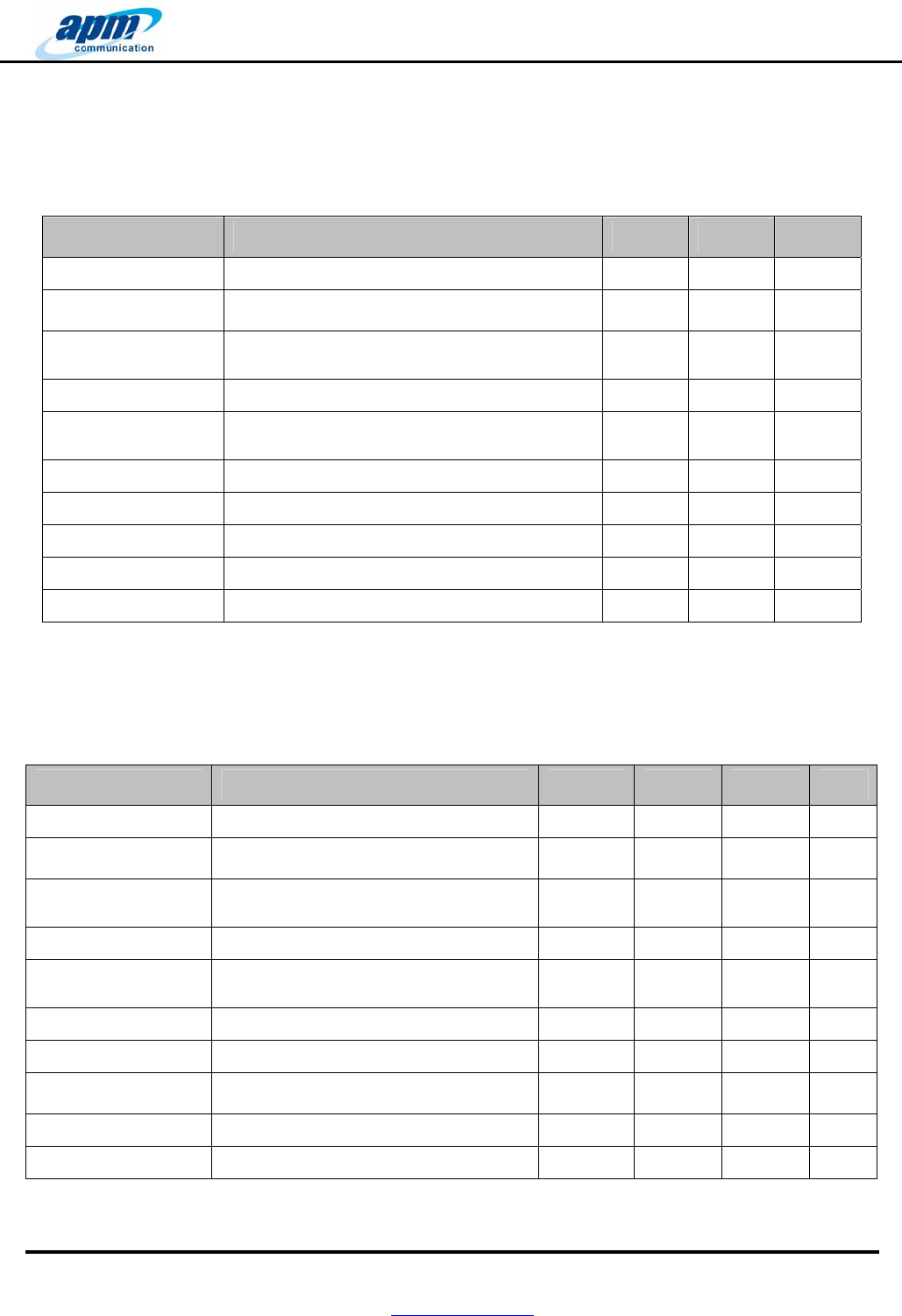
3 Mechanical Specification
Dimension 9×11×1.3 mm (max. height)
Pinout 56
Weight 0.3g
Antenna External antenna support (Pin 53)
3-1 Package Outline
apmcomm confidential
apm6658/6659 WiFi 802.11 b/g/n & BT2.1+EDR Dual Radio Module
Product Information Data Sheet
Page 28 of 30
apm Communication, Inc. – TEL: 886-3-666-1188 – FAX: 886-3-666-8033
Website: http://www.apmcomm.com – E-mail: sales@apmcomm.com
apmcomm Proprietary and Confidential – Product information is subject to change without notice.– May 30 2011
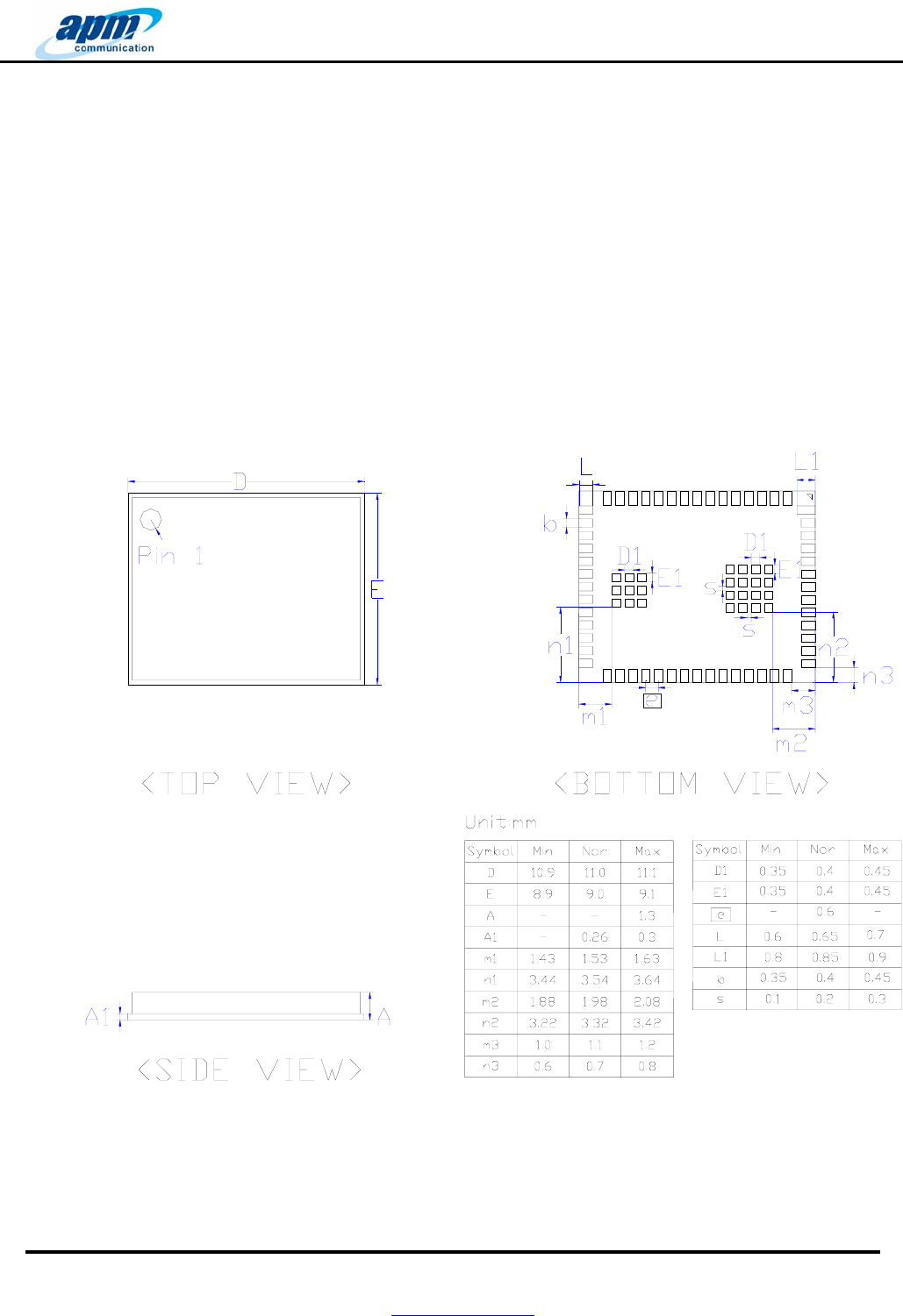
4 Assembly Guideline
4-1 Recommended Mounting Pad Design (Top View)
The following figure illustrates the recommended mounting pad design for apm6658/6659.
TOP VIEW (mm)
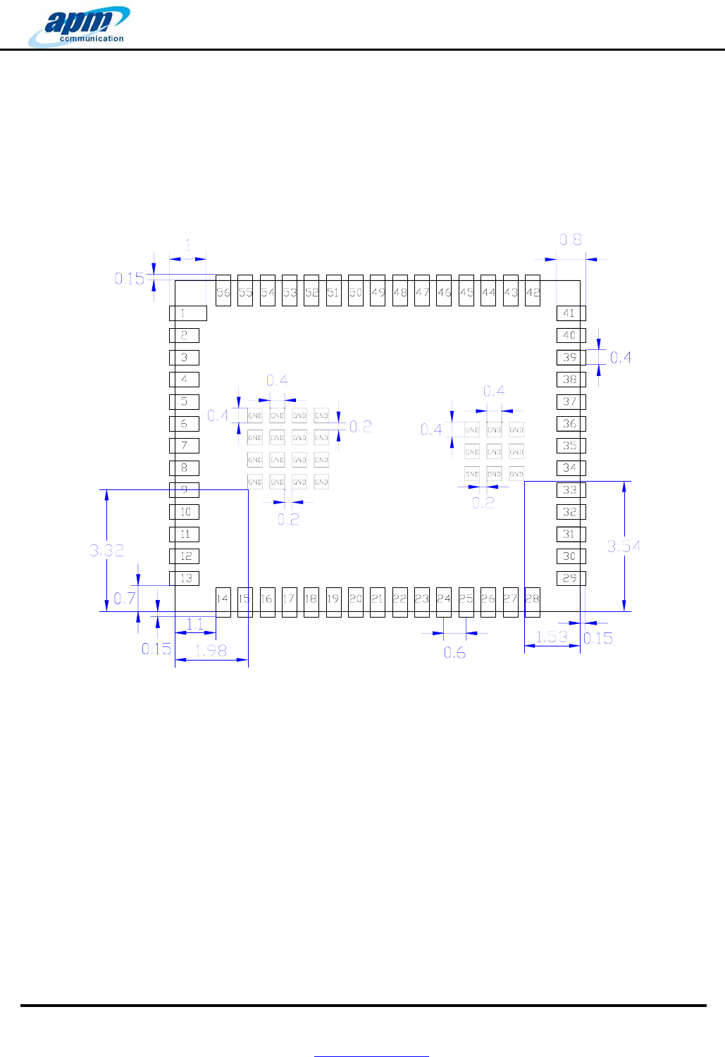
4-2 Recommendation for Stencil Aperture in SMT Process
Please follow general QFN stencil design guideline. Some rules of thumb are highlighted below.
‧ The LGA pads should NOT be flooded over with copper, they should be connected into the plane with a track
width of approx 50% of the pad width, this will mean more heat will be available at the joint. Track lengths should
obviously be minimized, we would generally use about 0.3mm on external layers.
apmcomm confidential
apm6658/6659 WiFi 802.11 b/g/n & BT2.1+EDR Dual Radio Module
Product Information Data Sheet
Page 29 of 30
apm Communication, Inc. – TEL: 886-3-666-1188 – FAX: 886-3-666-8033
Website: http://www.apmcomm.com – E-mail: sales@apmcomm.com
apmcomm Proprietary and Confidential – Product information is subject to change without notice.– May 30 2011
‧ The solder paste pattern for the internal Tab pads could be split into 4 smaller segments for the 2 large pads, and
2 smaller segments for the smaller pads, this should have the effect of preventing the paste from pooling into one area,
and hence minimize the likelihood of the pads being held away from each other. We use a rule of thumb of 50% solder
paste area in relation to Tab copper area (this only applies to tab pads under the device – not the signal pads).
‧ The thickness of the solder paste stencil has implications on solder joint quality as well, we do not have the
knowledge on what stencil should be specified.
‧ Ensure they are using a good appropriate flux, and the correct reflow profile for unleaded (basically +20C above
leaded) which is also uniform in nature.
Violating the basic rules might cause problems. For example, if the stencil apertures of the internal ground planes
are improperly big, they would hold more solders in SMT process and may cause the module peripheral pads
un-contacted to the main board. To improve this situation, apmcomm suggests the stencil opening shown as follows.
Stencil Aperture (Top View)
apmcomm confidential
apm6658/6659 WiFi 802.11 b/g/n & BT2.1+EDR Dual Radio Module
Product Information Data Sheet
Page 30 of 30
apm Communication, Inc. – TEL: 886-3-666-1188 – FAX: 886-3-666-8033
Website: http://www.apmcomm.com – E-mail: sales@apmcomm.com
apmcomm Proprietary and Confidential – Product information is subject to change without notice.– May 30 2011
4-3 Baking condition recommendation before IR reflow
Baking condition for apm6658/6659 module:
I: 125°C/4 hrs baking is necessary for apm6658/6659 module before SMT process. After baking treatment the
modules can be stored in the environment under 30°C and 60% RH for 48 hrs. If the storage time is over 48 hrs,
the modules need to be re-baked using the same condition again.
II: In the event that the sealed bag is damaged on receipt of the modules, the baking condition should be changed to
125°C/8 hrs.
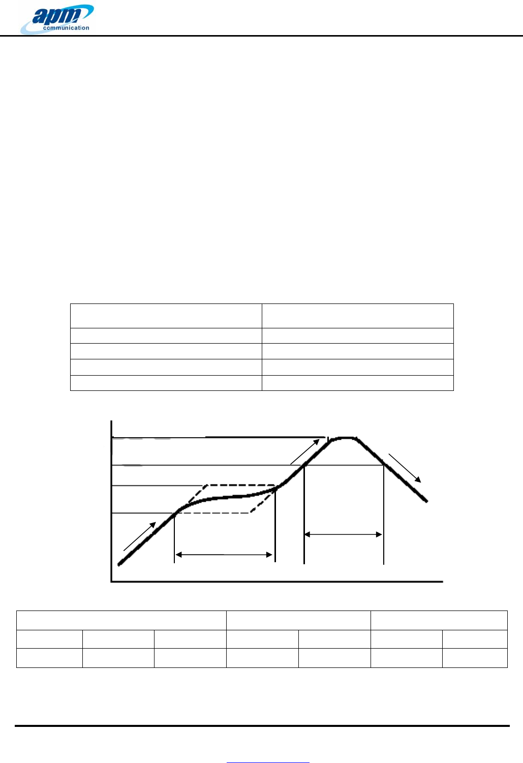
4-4 Recommendation for Reflow Profile
Maximum reflow temperature is 250°C.
Preheat ramp-up rate 125°C to 180°C
1 to 3°C /sec.
Peak temperature 250°C max.
Temperature maintained above 217°C 30 ~ 90 sec.
Cooling ramp-down rate <2°C/sec.
Maximum number of reflow cycles ≤3
Heating/Cooling Speed Pre-Heating Heating
ΔT1 ΔT2 ΔT3 Tp1−Tp2 tpre T
Max t
P3
1 to 3°C /sec. 1 to 3°C /sec. < 2°C /sec. 125 ~ 180°C 30 ~ 90 sec. 250°C max. 30 ~ 90 sec.
TMax
Tp3
Tp2
Tp1
TMax
Pre-heating
area tpre
210℃or more
10~60 sec.
ΔT1
ΔT2
ΔT3
217°C above
30 ~ 90 sec
t
P3
Time
Federal Communication Commission Interference Statement
This device complies with Part 15 of the FCC Rules. Operation is subject to the
following two conditions: (1) This device may not cause harmful interference, and
(2) this device must accept any interference received, including interference that may
cause undesired operation.
This equipment has been tested and found to comply with the limits for a Class B
digital device, pursuant to Part 15 of the FCC Rules. These limits are designed to
provide reasonable protection against harmful interference in a residential installation.
This equipment generates, uses and can radiate radio frequency energy and, if not
installed and used in accordance with the instructions, may cause harmful interference
to radio communications. However, there is no guarantee that interference will not
occur in a particular installation. If this equipment does cause harmful interference to
radio or television reception, which can be determined by turning the equipment off
and on, the user is encouraged to try to correct the interference by one of the
following measures:
- Reorient or relocate the receiving antenna.
- Increase the separation between the equipment and receiver.
- Connect the equipment into an outlet on a circuit different from that
to which the receiver is connected.
- Consult the dealer or an experienced radio/TV technician for help.
FCC Caution: Any changes or modifications not expressly approved by the party
responsible for compliance could void the user's authority to operate this equipment.
This transmitter must not be co-located or operating in conjunction with any other
antenna or transmitter.

Radiation Exposure Statement:
This equipment complies with FCC radiation exposure limits set forth for an
uncontrolled environment. This module can be used with Getac PDA: PS336 or
similar platform with similar dimension, antenna location and RF characteristic.
This device is intended only for OEM integrators under the following conditions:
1) The antenna must be installed at same location as tested in the certification filing.
2) The transmitter module may not be co-located with any other transmitter or
antenna.
3) For portable usage condition, this module has been SAR evaluated in Getac PDA:
PS336 host with compliance result and can be used with this specific hast as
described in the certification filing. Other host or platform needs separate approval.
As long as 3 conditions above are met, further transmitter test will not be required.
However, the OEM integrator is still responsible for testing their end-product for any
additional compliance requirements required with this module installed
IMPORTANT NOTE: In the event that these conditions can not be met (for example
certain laptop configurations or co-location with another transmitter), then the FCC
authorization is no longer considered valid and the FCC ID can not be used on the
final product. In these circumstances, the OEM integrator will be responsible for
re-evaluating the end product (including the transmitter) and obtaining a separate FCC
authorization.
End Product Labeling
The final end product must be labeled in a visible area with the following: “Contains
FCC ID: QYLAPM6658”. The grantee's FCC ID can be used only when all FCC
compliance requirements are met.
Manual Information To the End User
The OEM integrator has to be aware not to provide information to the end user
regarding how to install or remove this RF module in the user’s manual of the end
product which integrates this module.
The end user manual shall include all required regulatory information/warning as
show in this manual.