Getac Technology F110N RFID and NFC Module User Manual 1
Getac Technology Corporation RFID and NFC Module 1
UserManual.wiki
>
Getac Technology
>
F110N User Manual
>
User manual 1
Contents
1.
User manual 1
2.
User manual 2
User manual 1
Navigation menu
Upload a User Manual
Namespaces
Wiki Guide
HTML
PDF
Info
Views
User Manual
Discussion / Help
Navigation
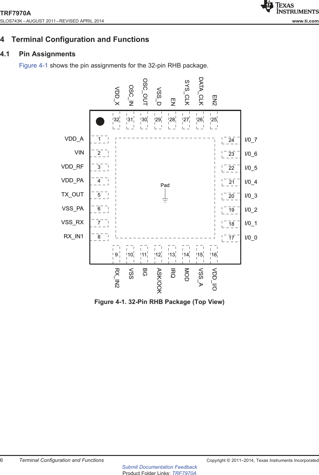
![MUXRX_IN1RX_IN2PHASE&AMPLITUDEDETECTORGAIN RSSI(AUX)LOGICLEVEL SHIFTERSTATECONTROLLOGIC[CONTROLREGISTERS &COMMANDLOGIC]127-BYTEFIFOMCUINTERFACEVDD_I/OI/O_0I/O_1I/O_2I/O_3I/O_4I/O_5I/O_6I/O_7IRQSYS_CLKDATA _CLKISOPROTOCOLHANDLING DECODERRSSI(EXTERNAL)PHASE&AMPLITUDEDETECTORGAINRSSI(MAIN)FILTER& AGC DIGITIZERBITFRAMINGFRAMINGSERIALCONVERSIONCRC & PARITYTRANSMITTER ANALOGFRONT ENDTX_OUTVDD_PAVSS_PADIGITAL CONTROLSTATE MACHINECRYSTAL OR OSCILLATORTIMING SYSTEMENEN2ASK/OOKMODOSC_INOSC_OUTVOLTAGE SUPPLY REGULATOR SYSTEMS(SUPPLY REGULATORS AND REFERENCE VOLTAGES)VSS_AVSS_RFVDD_RFVDD_XVSS_DVSSVINVDD_ABAND_GAPRF LEVELDETECTORTRF7970ASLOS743K –AUGUST 2011–REVISED APRIL 2014www.ti.com1.4 Functional Block DiagramFigure 1-1 shows the block diagram.Figure 1-1. Block Diagram2Device Overview Copyright © 2011–2014, Texas Instruments IncorporatedSubmit Documentation FeedbackProduct Folder Links: TRF7970A](https://usermanual.wiki/Getac-Technology/F110N.User-manual-1/User-Guide-2883830-Page-2.png)