Getac Technology F110N RFID and NFC Module User Manual 1
Getac Technology Corporation RFID and NFC Module 1
Contents
- 1. User manual 1
- 2. User manual 2
User manual 1
Product
Folder
Sample &
Buy
Technical
Documents
Tools &
Software
Support &
Community
Reference
Design
TRF7970A
SLOS743K –AUGUST 2011–REVISED APRIL 2014
TRF7970A Multiprotocol Fully Integrated 13.56-MHz RFID and Near Field Communication
(NFC) Transceiver IC
1 Device Overview
1.1 Features
1
• Supports Near Field Communication (NFC) • Programmable Output Power: +20 dBm (100 mW),
Standards NFCIP-1 (ISO/IEC 18092) and NFCIPತ2 +23 dBm (200 mW)
(ISO/IEC 21481) • Programmable I/O Voltage Levels From 1.8 VDC
• Completely Integrated Protocol Handling for to 5.5 VDC
ISO15693, ISO18000-3, ISO14443A/B, and • Programmable System Clock Frequency Output
FeliCa™ (RF, RF/2, RF/4) from 13.56-MHz or 27.12-MHz
• Integrated Encoders, Decoders, and Data Framing Crystal or Oscillator
for NFC Initiator, Active and Passive Target • Integrated Voltage Regulator Output for Other
Operation for All Three Bit Rates (106 kbps, System Components (MCU, Peripherals,
212 kbps, 424 kbps) and Card Emulation Indicators), 20 mA (Max)
• RF Field Detector With Programmable Wake-Up • Programmable Modulation Depth
Levels for NFC Passive Transponder Emulation • Dual Receiver Architecture With RSSI for
Operation Elimination of "Read Holes" and Adjacent Reader
• RF Field Detector for NFC Physical Collision System or Ambient In-Band Noise Detection
Avoidance. • Programmable Power Modes for Ultra Low-Power
• Integrated State Machine for ISO14443A System Design (Power Down <1 µA)
Anticollision (Broken Bytes) Operation • Parallel or SPI Interface (With 127-Byte FIFO)
(Transponder Emulation or NFC Passive Target) • Temperature Range: –40°C to 110°C
• Input Voltage Range: 2.7 VDC to 5.5 VDC • 32-Pin QFN Package (5 mm x 5 mm)
1.2 Applications
• Mobile Devices (Tablets, Handsets) • Short-Range Wireless Communication Tasks
(Firmware Updates)
• Secure Pairing ( Bluetooth®, Wi-Fi®, Other Paired
Wireless Networks) • Product Identification or Authentication
• Public Transport or Event Ticketing • Medical Equipment or Consumables
• Passport or Payment (POS) Reader Systems • Access Control, Digital Door Locks
• Sharing of Electronic Business Cards
1.3 Description
The TRF7970A device is an integrated analog front end and data-framing device for a 13.56-MHz RFID
and Near Field Communication (NFC) system. Built-in programming options make the device suitable for a
wide range of applications for proximity and vicinity identification systems.
The device can perform in one of three modes: RFID and NFC reader, NFC peer, or in card emulation
mode. Built-in user-configurable programming options make the device suitable for a wide range of
applications. The TRF7970A device is configured by selecting the desired protocol in the control registers.
Direct access to all control registers allows fine tuning of various reader parameters as needed.
Documentation, reference designs, EVM, and source code TI MSP430™ MCUs or ARM®MCUs are
available.
Device Information
PART NUMBER PACKAGE BODY SIZE
TRF7970ARHB VQFN (32) 5 mm x 5 mm
1
An IMPORTANT NOTICE at the end of this data sheet addresses availability, warranty, changes, use in safety-critical applications,
intellectual property matters and other important disclaimers. PRODUCTION DATA.
MUX
RX_IN1
RX_IN2
PHASE&
AMPLITUDE
DETECTOR
GAIN RSSI
(AUX)
LOGIC
LEVEL SHIFTER
STATE
CONTROL
LOGIC
[CONTROL
REGISTERS &
COMMAND
LOGIC]
127-BYTE
FIFO
MCU
INTERFACE
VDD_I/O
I/O_0
I/O_1
I/O_2
I/O_3
I/O_4
I/O_5
I/O_6
I/O_7
IRQ
SYS_CLK
DATA _CLK
ISO
PROTOCOL
HANDLING DECODER
RSSI
(EXTERNAL)
PHASE&
AMPLITUDE
DETECTOR
GAIN
RSSI
(MAIN)
FILTER
& AGC DIGITIZER
BIT
FRAMING
FRAMING
SERIAL
CONVERSION
CRC & PARITY
TRANSMITTER ANALOG
FRONT END
TX_OUT
VDD_PA
VSS_PA
DIGITAL CONTROL
STATE MACHINE
CRYSTAL OR OSCILLATOR
TIMING SYSTEM
EN
EN2
ASK/OOK
MOD
OSC_IN
OSC_OUT
VOLTAGE SUPPLY REGULATOR SYSTEMS
(SUPPLY REGULATORS AND REFERENCE VOLTAGES)
VSS_A
VSS_RF
VDD_RF
VDD_X
VSS_D
VSS
VIN
VDD_A
BAND_GAP
RF LEVEL
DETECTOR
TRF7970A
SLOS743K –AUGUST 2011–REVISED APRIL 2014
www.ti.com
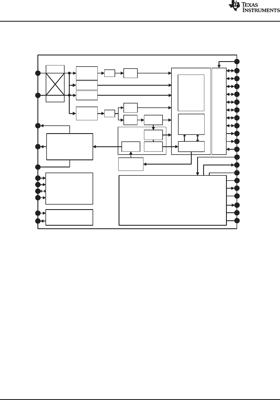
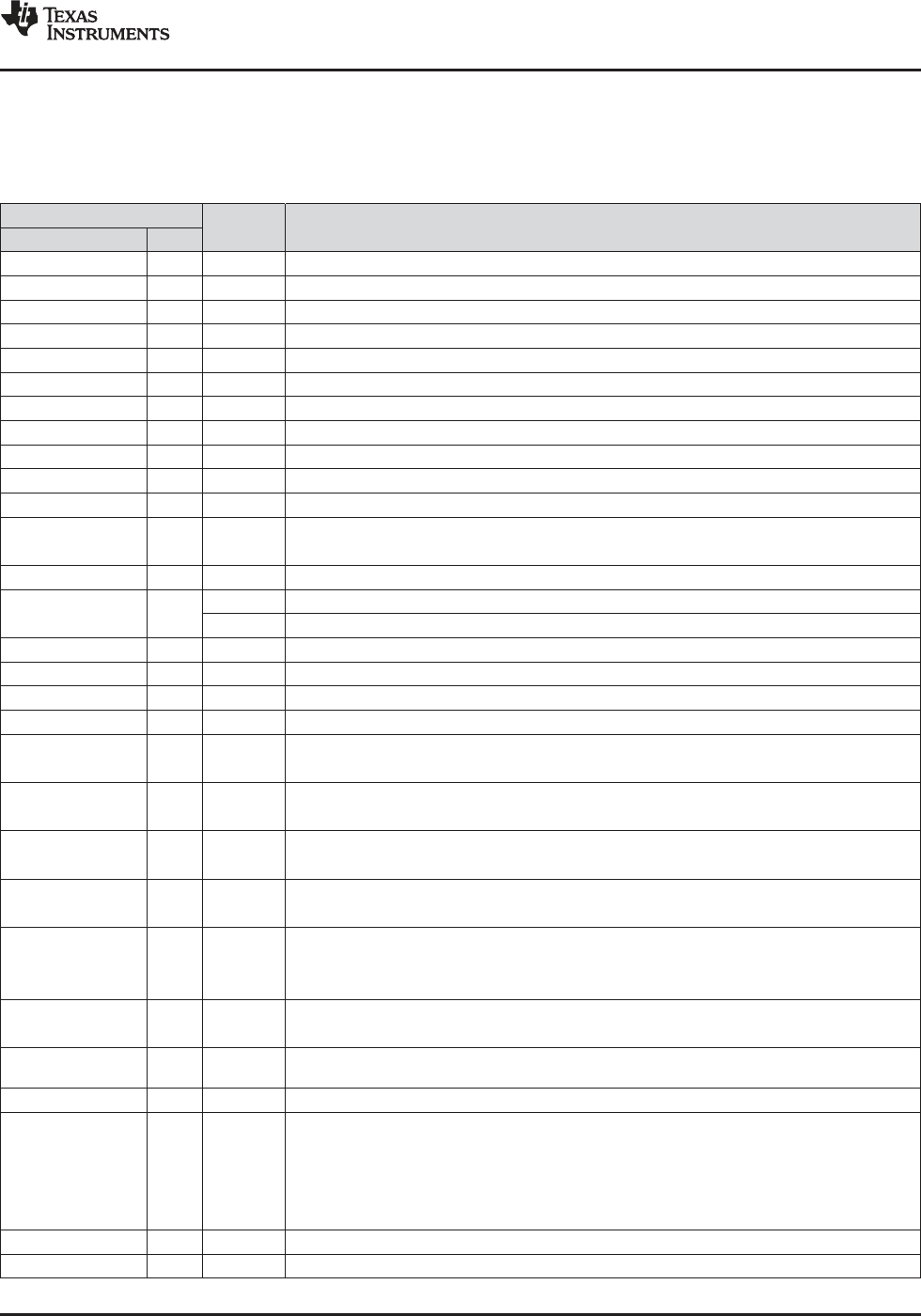
1.4 Functional Block Diagram
Figure 1-1 shows the block diagram.
Figure 1-1. Block Diagram
2Device Overview Copyright © 2011–2014, Texas Instruments Incorporated
Submit Documentation Feedback
Product Folder Links: TRF7970A
TRF7970A
www.ti.com
SLOS743K –AUGUST 2011–REVISED APRIL 2014
Table of Contents
1 Device Overview ......................................... 16.8 Transmitter – Digital Section ........................ 28
6.9 Transmitter – External Power Amplifier and
1.1 Features .............................................. 1
Subcarrier Detector ................................. 29
1.2 Applications........................................... 1
6.10 TRF7970A IC Communication Interface ............ 30
1.3 Description............................................ 1
6.11 Special Direct Mode for Improved MIFARE™
1.4 Functional Block Diagram ............................ 2Compatibility......................................... 48
2 Revision History ......................................... 46.12 NFC Modes.......................................... 48
3 Device Characteristics.................................. 56.13 Direct Commands from MCU to Reader ............ 51
4 Terminal Configuration and Functions.............. 66.14 Register Description................................. 55
4.1 Pin Assignments...................................... 67 Application Schematic and Layout
4.2 Terminal Functions ................................... 7Considerations.......................................... 75
5 Specifications ............................................ 97.1 TRF7970A Reader System Using Parallel
Microcontroller Interface............................. 75
5.1 Absolute Maximum Ratings .......................... 9
7.2 TRF7970A Reader System Using SPI With SS
5.2 Recommended Operating Conditions ................ 9
Mode ................................................ 76
5.3 Electrical Characteristics ............................ 10
7.3 Layout Considerations .............................. 77
5.4 Handling Ratings .................................... 11
7.4 Impedance Matching TX_Out (Pin 5) to 50 ...... 77
5.5 Thermal Characteristics ............................. 11
7.5 Reader Antenna Design Guidelines ................ 79
5.6 Switching Characteristics ........................... 11
8 Device and Documentation Support ............... 80
6 Detailed Description ................................... 12
8.1 Documentation Support ............................. 80
6.1 Overview ............................................ 12
8.2 Community Resources .............................. 80
6.2 System Block Diagram .............................. 15
8.3 Trademarks.......................................... 80
6.3 Power Supplies...................................... 15
8.4 Electrostatic Discharge Caution..................... 80
6.4 Receiver – Analog Section .......................... 21
8.5 Glossary ............................................. 80
6.5 Receiver – Digital Section ........................... 22
9 Mechanical Packaging and Orderable
6.6 Oscillator Section ................................... 27 Information .............................................. 80
6.7 Transmitter – Analog Section ....................... 28 9.1 Packaging Information .............................. 80
Copyright © 2011–2014, Texas Instruments Incorporated Table of Contents 3
Submit Documentation Feedback
Product Folder Links: TRF7970A

TRF7970A
SLOS743K –AUGUST 2011–REVISED APRIL 2014
www.ti.com
2 Revision History
NOTE: Page numbers for previous revisions may differ from page numbers in the current version.
Changes from Revision J (February 2014) to Revision K Page
• Changed Figure 1-1 to show 127-byte FIFO...................................................................................... 2
• Moved Section 3 ...................................................................................................................... 5
• Changed title of Section 4 .......................................................................................................... 6
• Changed title of Section 5 ........................................................................................................... 9
• Added ASK/OOK and MOD to VIL and VIH ........................................................................................ 9
• Moved Section 5.3 .................................................................................................................. 10
• Changed VDD_A TYP value from 3.5 V to 3.4 V ................................................................................. 10
• Moved Section 5.4 .................................................................................................................. 11
• Added V(ESD) MIN values, test specifications, and notes....................................................................... 11
• Changed title of Section 5.5 from Dissipation Ratings to Thermal Characteristics ......................................... 11
• Moved Section 5.6 .................................................................................................................. 11
• Changed title of Section 6.......................................................................................................... 12
• Moved previous Section 3, Device Overview, to Section 6.1.................................................................. 12
• Changed from "By default, the AGC is frozen after..." to "By default, the AGC window comparator is set after..." ... 21
• Changed from "TX Pulse Length Control register (0x05)" to "TX Pulse Length Control register (0x06)" ............... 28
• Changed from "18.8 s" to "18.8 µs" in the sentence that starts with "If the register contains all zeros..."............... 28
• Changed Table 6-18 to match Table 6-43 ....................................................................................... 50
• Changed command 0x18 to "Test internal RF" ................................................................................. 51
• Changed command 0x19 to "Test external RF" ................................................................................ 51
• Moved Section 6.14 ................................................................................................................. 55
• Changed the sentence that starts "The AGC action is fast..." from "finishes after four subcarrier pulses" to
"finishes within eight subcarrier pulses" ......................................................................................... 64
• Moved Section 7..................................................................................................................... 75
• Deleted previous Section 10, System Design, and moved contents to Section 7.3 through Section 7.5 ............... 77
• Removed references to figure numbers in Figure 7-3.......................................................................... 78
4Revision History Copyright © 2011–2014, Texas Instruments Incorporated
Submit Documentation Feedback
Product Folder Links: TRF7970A

TRF7970A
www.ti.com
SLOS743K –AUGUST 2011–REVISED APRIL 2014
3 Device Characteristics
Table 3-1 shows the supported modes of operation for the TRF7970A device.
Table 3-1. Supported Modes of Operation
P2P Initiator or Reader/Writer Card Emulation P2P Target
Bit rate Bit rate Bit rate
Technology Technology Technology
(kbps) (kbps) (kbps)
106, 212, 424,
NFC-A/B (ISO14443A/B) NFC-A/B 106 NFC-A 106
848(1)
NFC-F (JIS: X6319-4) 212, 424 N/A N/A NFC-F 212, 424
NFC-V (ISO15693) 6.7, 26.7 N/A N/A N/A N/A
(1) 848 kbps only applies to reader/writer mode.
Copyright © 2011–2014, Texas Instruments Incorporated Device Characteristics 5
Submit Documentation Feedback
Product Folder Links: TRF7970A
VDD_A
VIN
VDD_RF
VDD_PA
TX_OUT
VSS_PA
VSS_RX
RX_IN1
I/0_7
RX_IN2
VSS
BG
ASK/OOK
IRQ
MOD
VSS_A
VDD_I/O
Pad
VDD_X
OSC_IN
OSC_OUT
VSS_D
EN
SYS_CLK
DATA_CLK
EN2
1
2
3
4
5
6
7
8
24
23
22
21
20
19
18
17
9 10 11 12 13 14 15 16
32 31 30 29 28 27 26 25
I/0_6
I/0_5
I/0_4
I/0_3
I/0_2
I/0_1
I/0_0
TRF7970A
SLOS743K –AUGUST 2011–REVISED APRIL 2014
www.ti.com
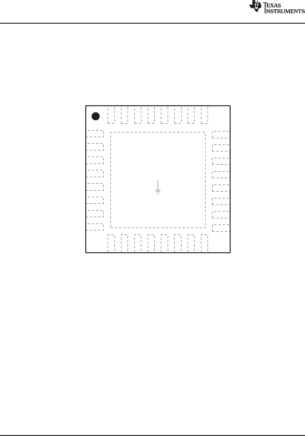
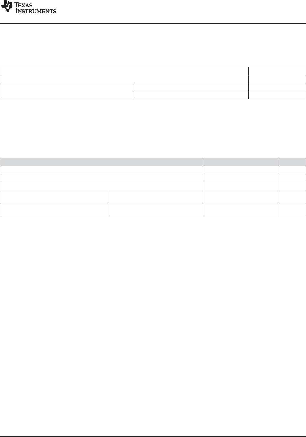
4 Terminal Configuration and Functions
4.1 Pin Assignments
Figure 4-1 shows the pin assignments for the 32-pin RHB package.
Figure 4-1. 32-Pin RHB Package (Top View)
6Terminal Configuration and Functions Copyright © 2011–2014, Texas Instruments Incorporated
Submit Documentation Feedback
Product Folder Links: TRF7970A
TRF7970A
www.ti.com
SLOS743K –AUGUST 2011–REVISED APRIL 2014
4.2 Terminal Functions
Table 4-1 describes the signals.
Table 4-1. Terminal Functions
TERMINAL TYPE (1) DESCRIPTION
NAME NO.
VDD_A 1 OUT Internal regulated supply (2.7 V to 3.4 V) for analog circuitry
VIN 2 SUP External supply input to chip (2.7 V to 5.5 V)
VDD_RF 3 OUT Internal regulated supply (2.7 V to 5 V), normally connected to VDD_PA (pin 4)
VDD_PA 4 INP Supply for PA; normally connected externally to VDD_RF (pin 3)
TX_OUT 5 OUT RF output (selectable output power, 100 mW or 200 mW, with VDD = 5 V)
VSS_PA 6 SUP Negative supply for PA; normally connected to circuit ground
VSS_RX 7 SUP Negative supply for RX inputs; normally connected to circuit ground
RX_IN1 8 INP Main RX input
RX_IN2 9 INP Auxiliary RX input
VSS 10 SUP Chip substrate ground
BAND_GAP 11 OUT Bandgap voltage (VBG = 1.6 V); internal analog voltage reference
Selection between ASK and OOK modulation (0 = ASK, 1 = OOK) for Direct Mode 0 or 1.
ASK/OOK 12 BID Can be configured as an output to provide the received analog signal output.
IRQ 13 OUT Interrupt request
INP External data modulation input for Direct Mode 0 or 1
MOD 14 OUT Subcarrier digital data output (see registers 0x1A and 0x1B)
VSS_A 15 SUP Negative supply for internal analog circuits; connected to GND
VDD_I/O 16 INP Supply for I/O communications (1.8 V to VIN) level shifter. VIN should be never exceeded.
I/O_0 17 BID I/O pin for parallel communication
I/O_1 18 BID I/O pin for parallel communication
I/O pin for parallel communication
I/O_2 19 BID TX Enable (in Special Direct Mode)
I/O pin for parallel communication
I/O_3 20 BID TX Data (in Special Direct Mode)
I/O pin for parallel communication
I/O_4 21 BID Slave Select signal in SPI mode
I/O pin for parallel communication
I/O_5 22 BID Data clock output in Direct Mode 1 and Special Direct Mode
I/O pin for parallel communication
I/O_6 23 BID MISO for serial communication (SPI)
Serial bit data output in Direct Mode 1 or subcarrier signal in Direct Mode 0
I/O pin for parallel communication.
I/O_7 24 BID MOSI for serial communication (SPI)
Selection of power down mode. If EN2 is connected to VIN, then VDD_X is active during power
EN2 25 INP down mode 2 (for example, to supply the MCU).
DATA_CLK 26 INP Data Clock input for MCU communication (parallel and serial)
If EN = 1 (EN2 = don't care) the system clock for MCU is configured. Depending on the crystal
that is used, options are as follows (see register 0x09):
SYS_CLK 27 OUT 13.56-MHz crystal: Off, 3.39 MHz, 6.78 MHz, or 13.56 MHz
27.12-MHz crystal: Off, 6.78 MHz, 13.56 MHz, or 27.12 MHz
If EN = 0 and EN2 = 1, then system clock is set to 60 kHz
EN 28 INP Chip enable input (If EN = 0, then chip is in sleep or power-down mode).
VSS_D 29 SUP Negative supply for internal digital circuits
(1) SUP = Supply, INP = Input, BID = Bidirectional, OUT = Output
Copyright © 2011–2014, Texas Instruments Incorporated Terminal Configuration and Functions 7
Submit Documentation Feedback
Product Folder Links: TRF7970A

TRF7970A
SLOS743K –AUGUST 2011–REVISED APRIL 2014
www.ti.com
Table 4-1. Terminal Functions (continued)
TERMINAL TYPE (1) DESCRIPTION
NAME NO.
OSC_OUT 30 OUT Crystal or oscillator output
INP Crystal or oscillator input
OSC_IN 31 OUT Crystal oscillator output
Internally regulated supply (2.7 V to 3.4 V) for digital circuit and external devices (for example,
VDD_X 32 OUT MCU)
Thermal Pad PAD SUP Chip substrate ground
8Terminal Configuration and Functions Copyright © 2011–2014, Texas Instruments Incorporated
Submit Documentation Feedback
Product Folder Links: TRF7970A
TRF7970A
www.ti.com
SLOS743K –AUGUST 2011–REVISED APRIL 2014
5 Specifications
5.1 Absolute Maximum Ratings (1) (2)
over operating free-air temperature range (unless otherwise noted)
VIN Input voltage range -0.3 V to 6 V
IIN Maximum current VIN 150 mA
Any condition 140°C
TJMaximum operating virtual junction temperature Continuous operation, long-term reliability (3) 125°C
(1) Stresses beyond those listed under Absolute Maximum Ratings may cause permanent damage to the device. These are stress ratings
only and functional operation of the device at these or any other conditions beyond those indicated under Operating Conditions are not
implied. Exposure to absolute-maximum-rated conditions for extended periods may affect device reliability.
(2) All voltage values are with respect to substrate ground terminal VSS.
(3) The maximum junction temperature for continuous operation is limited by package constraints. Operation above this temperature may
result in reduced reliability or lifetime of the device.
5.2 Recommended Operating Conditions
over operating free-air temperature range (unless otherwise noted)
MIN TYP MAX UNIT
VIN Operating input voltage 2.7 5 5.5 V
TAOperating ambient temperature -40 25 110 °C
TJOperating virtual junction temperature -40 25 125 °C
I/O lines, IRQ, SYS_CLK, DATA_CLK, 0.2 x
VIL Input voltage - logic low V
EN, EN2, ASK/OOK, MOD VDD_I/O
I/O lines, IRQ, SYS_CLK, DATA_CLK, 0.8 x
VIH Input voltage threshold, logic high V
EN, EN2, ASK/OOK, MOD VDD_I/O
Copyright © 2011–2014, Texas Instruments Incorporated Specifications 9
Submit Documentation Feedback
Product Folder Links: TRF7970A

TRF7970A
SLOS743K –AUGUST 2011–REVISED APRIL 2014
www.ti.com
5.3 Electrical Characteristics
TYP operating conditions are TA= 25°C, VIN = 5 V, full-power mode (unless otherwise noted)
MIN and MAX operating conditions are over recommended ranges of supply voltage and operating free-air temperature
(unless otherwise noted)
PARAMETER TEST CONDITIONS MIN TYP MAX UNIT
All building blocks disabled, including supply-
IPD1 Supply current in Power Down Mode 1 voltage regulators; measured after 500-ms 0.5 5 µA
settling time (EN = 0, EN2 = 0)
The SYS_CLK generator and VDD_X remain
Supply current in Power Down Mode 2
IPD2 active to support external circuitry; measured 120 200 µA
(Sleep Mode) after 100-ms settling time (EN = 0, EN2 = 1)
Oscillator running, supply-voltage regulators in
ISTBY Supply current in stand-by mode 1.9 3.5 mA
low-consumption mode (EN = 1, EN2 = x)
Supply current without antenna driver Oscillator, regulators, RX and AGC active, TX
ION1 10.5 14 mA
current is off
Oscillator, regulators, RX and AGC and TX
ION2 Supply current – TX (half power) 70 78 mA
active, POUT = 100 mW
Oscillator, regulators, RX and AGC and TX
ION3 Supply current – TX (full power) 130 150 mA
active, POUT = 200 mW
VPOR Power-on reset voltage Input voltage at VIN 1.4 2 2.6 V
VBG Bandgap voltage (pin 11) Internal analog reference voltage 1.5 1.6 1.7 V
Regulated output voltage for analog
VDD_A VIN = 5 V 3.1 3.4 3.8 V
circuitry (pin 1)
VDD_X Regulated supply for external circuitry Output voltage pin 32, VIN = 5 V 3.1 3.4 3.8 V
IVDD_Xmax Maximum output current of VDD_X Output current pin 32, VIN = 5 V 20 mA
Half-power mode, VIN = 2.7 V to 5.5 V 8 12
RRFOUT Antenna driver output resistance (1) ȍ
Full-power mode, VIN = 2.7 V to 5.5 V 4 6
RRFIN RX_IN1 and RX_IN2 input resistance 4 10 20 kȍ
Maximum RF input voltage at RX_IN1 and
VRF_INmax VRF_INmax should not exceed VIN 3.5 Vpp
RX_IN2
fSUBCARRIER= 424 kHz 1.4 2.5
Minimum RF input voltage at RX_IN1 and
VRF_INmin mVpp
RX_IN2 (input sensitivity)(2) fSUBCARRIER = 848 kHz 2.1 3
fSYS_CLK SYS_CLK frequency In power mode 2, EN = 0, EN2 = 1 25 60 120 kHz
fCCarrier frequency Defined by external crystal 13.56 MHz
Time until oscillator stable bit is set (register
tCRYSTAL Crystal run-in time 3 ms
0x0F)(3)
Depends on capacitive load on the I/O lines,
fD_CLKmax Maximum DATA_CLK frequency(4) 2 8 10 MHz
recommendation is 2 MHz(4)
ROUT Output resistance I/O_0 to I/O_7 500 800 ȍ
RSYS_CLK Output resistance RSYS_CLK 200 400 ȍ
(1) Antenna driver output resistance
(2) Measured with subcarrier signal at RX_IN1 or RX_IN2 and measured the digital output at MOD pin with register 0x1A bit 6 = 1.
(3) Depends on the crystal parameters and components
(4) Recommended DATA_CLK speed is 2 MHz. Higher data clock depends on the capacitive load. Maximum SPI clock speed should not
exceed 10 MHz. This clock speed is acceptable only when external capacitive load is less than 30 pF. MISO driver has a typical output
resistance of 400 ȍ(12-ns time constant when 30-pF load used).
10 Specifications Copyright © 2011–2014, Texas Instruments Incorporated
Submit Documentation Feedback
Product Folder Links: TRF7970A
TRF7970A
www.ti.com
SLOS743K –AUGUST 2011–REVISED APRIL 2014
5.4 Handling Ratings
MIN MAX UNIT
TSTG Storage temperature range -55 150 °C
V(ESD) Electrostatic discharge Human-Body Model (HBM), per ANSI/ESDA/JEDEC JS-001, all pins(1) -2 2 kV
Charged-Device Model (CDM), per JEDEC specification JESD22-C101, -500 500 V
all pins(2)
Machine Model (MM) -200 200 V
(1) JEDEC document JEP155 states that 500-V HBM allows safe manufacturing with a standard ESD control process. Pins listed as 2 kV
may actually have higher performance.
(2) JEDEC document JEP157 states that 250-V CDM allows safe manufacturing with a standard ESD control process. Pins listed as 500 V
may actually have higher performance.
5.5 Thermal Characteristics
POWER RATING(2)
PACKAGE șJC șJA(1)
TA25°C TA85°C
RHB (32 pin) 31°C/W 36.4°C/W 2.7 W 1.1 W
(1) This data was taken using the JEDEC standard high-K test PCB.
(2) Power rating is determined with a junction temperature of 125°C. This is the point where distortion starts to increase substantially.
Thermal management of the final PCB should strive to keep the junction temperature at or below 125°C for best performance and long-
term reliability.
5.6 Switching Characteristics
TYP operating conditions are TA= 25°C, VIN = 5 V, full-power mode (unless otherwise noted)
MIN and MAX operating conditions are over recommended ranges of supply voltage and operating free-air temperature
(unless otherwise noted)
PARAMETER TEST CONDITIONS MIN TYP MAX UNIT
DATA_CLK time high or low, one half of
tLO/HI Depends on capacitive load on the I/O lines(1) 250 62.5 50 ns
DATA_CLK at 50% duty cycle
Slave select lead time, slave select low to
tSTE,LEAD 200 ns
clock
Slave select lag time, last clock to slave
tSTE,LAG 200 ns
select high
Slave select disable time, slave select
tSTE,DIS rising edge to next slave select falling 300 ns
edge
tSU,SI MOSI input data setup time 15 ns
tHD,SI MOSI input data hold time 15 ns
tSU,SO MISO input data setup time 15 ns
tHD,SO MISO input data hold time 15 ns
tVALID,SO MISO output data valid time DATA_CLK edge to MISO valid, CL30 pF 30 50 75 ns
(1) Recommended DATA_CLK speed is 2 MHz. Higher data clock depends on the capacitive load. Maximum SPI clock speed should not
exceed 10 MHz. This clock speed is acceptable only when external capacitive load is less than 30 pF. MISO driver has a typical output
resistance of 400 ȍ(12-ns time constant when 30-pF load used).
Copyright © 2011–2014, Texas Instruments Incorporated Specifications 11
Submit Documentation Feedback
Product Folder Links: TRF7970A
Federal Communication Commission Interference Statement
This device complies with Part 15 of the FCC Rules. Operation is subject to the
following two conditions: (1) This device may not cause harmful interference, and (2)
this device must accept any interference received, including interference that may
cause undesired operation.
This equipment has been tested and found to comply with the limits for a Class B
digital device, pursuant to Part 15 of the FCC Rules. These limits are designed to
provide reasonable protection against harmful interference in a residential installation.
This equipment generates uses and can radiate radio frequency energy and, if not
installed and used in accordance with the instructions, may cause harmful interference
to radio communications. However, there is no guarantee that interference will not
occur in a particular installation. If this equipment does cause harmful interference to
radio or television reception, which can be determined by turning the equipment off
and on, the user is encouraged to try to correct the interference by one of the
following measures:
Reorient or relocate the receiving antenna.
Increase the separation between the equipment and receiver.
Connect the equipment into an outlet on a circuit different from that
to which the receiver is connected.
Consult the dealer or an experienced radio/TV technician for help.
FCC Caution:
Any changes or modifications not expressly approved by the party responsible
for compliance could void the user's authority to operate this equipment.
This transmitter must not be co-located or operating in conjunction with any
other antenna or transmitter.

Radiation Exposure Statement:
The product is a low power device and its output power is lower than FCC SAR
exemption level. This module can be used with Product name: F110.
This device is intended only for OEM integrators under the following conditions:
1) The transmitter module may not be co-located with any other transmitter or
antenna. The co-transmitting with other radio will need a separate evaluation.
2) Module approval valid only when this module is installed in the tested host
“Product name: F110”.
As long as 2 conditions above are met, further transmitter test will not be required.
However, the OEM integrator is still responsible for testing their end-product for any
additional compliance requirements required with this module installed
IMPORTANT NOTE: In the event that these conditions cannot be met (for example
certain laptop configurations or co-location with another transmitter), then the FCC
authorization is no longer considered valid and the FCC ID cannot be used on the
final product. In these circumstances, the OEM integrator will be responsible for
re-evaluating the end product (including the transmitter) and obtaining a separate FCC
authorization.
End Product Labeling
The final end product must be labeled in a visible area with the following: “Contains
FCC ID: QYLF110N”. The grantee's FCC ID can be used only when all FCC
compliance requirements are met.
Manual Information to the End User
The OEM integrator has to be aware not to provide information to the end user
regarding how to install or remove this RF module in the user’s manual of the end
product which integrates this module.
The end user manual shall include all required regulatory information/warning as
show in this manual.