Gigawit Electronics GWNO GWK5Nx 2.4 GHz Wireless Audio Transmitter / Receiver User Manual Manual
Gigawit Electronics Limited GWK5Nx 2.4 GHz Wireless Audio Transmitter / Receiver Manual
UserManual.wiki
>
Gigawit Electronics
>
GWNO User Manual
>
Manual
Contents
1.
Manual
2.
Addendum
Manual
Navigation menu
Upload a User Manual
Namespaces
Wiki Guide
HTML
PDF
Info
Views
User Manual
Discussion / Help
Navigation
![©2008-2011 Gigawit Electronics Ltd. Version 1.0 Page 3 of 17 GWK5Nx Datasheet 5. Electrical Specification Table [1]: Electrical Specification Description Typical Operation voltage +3.3V DC Supply current TX: 60mA RX: 60mA (GWK5NO) TX: 69mA RX: 63mA (GWK5NQ) General Operation temperature -10 ~ +60℃ RF Frequency 2400 ~ 2483MHZ Modulation GFSK Data rate 2M bps TX Power +0dBm (GWK5NO) +10dBm (GWK5NQ) RX Sensitivity -90dBm (GWK5NO) -88dBm (GWK5NQ) RF RF Range (indoor) 10m (GWK5NO) 15m (GWK5NQ) Frequency Response 20~20KHz S/N >85dB @ 20~20KHz THD+N < 0.01% @ 20~20KHz Dynamic range 80dB Digital Audio Format I2S, Left Justify, Right Justify Sample Rate Support 32KHz, 44.1KHz, 48KHz Audio Latency Fixed 15ms or application dependent](https://usermanual.wiki/Gigawit-Electronics/GWNO.Manual/User-Guide-1821486-Page-3.png)
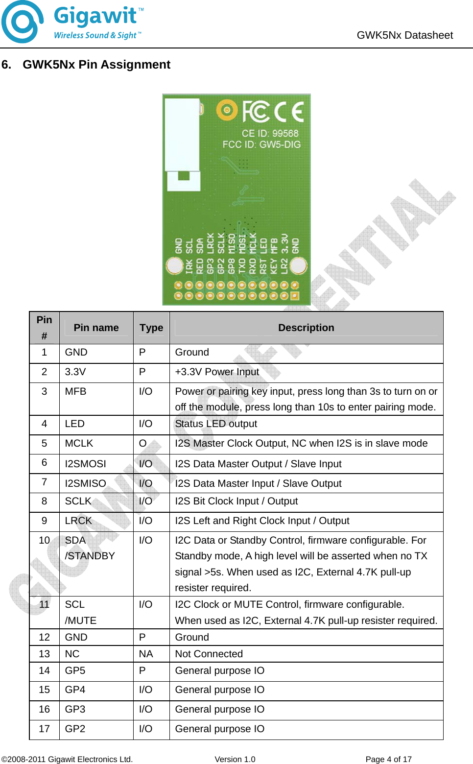
![©2008-2011 Gigawit Electronics Ltd. Version 1.0 Page 5 of 17 GWK5Nx Datasheet 18 GP8 I/O General purpose IO 19 TXD I/O UART TX 20 RXD I/O UART RX 21 RST I Reset input, active low 22 KEY I/O Built-in ADC for KEY 23 LR2 I 192 KHz sampling rate LRCK input 24 NC NA Not Connected Table [2]. GWK5Nx Pin Description](https://usermanual.wiki/Gigawit-Electronics/GWNO.Manual/User-Guide-1821486-Page-5.png)
![©2008-2011 Gigawit Electronics Ltd. Version 1.0 Page 6 of 17 GWK5Nx Datasheet 7. Application Schematic R12KLRCKSCLKSDINSDASCLTo DSP I2S OutputGND3.3VINMFBLEDSCLSDAMOSISCLKMCLKLRCKGNDMISOGWK5NxKEYD1LED+3. 3VTo MCU I2C Control Figure [1]: GWK5Nx Interfacing with DSP (I2S Slave Input Mode)](https://usermanual.wiki/Gigawit-Electronics/GWNO.Manual/User-Guide-1821486-Page-6.png)
![©2008-2011 Gigawit Electronics Ltd. Version 1.0 Page 7 of 17 GWK5Nx Datasheet I2SMCLKI2SLRCKI2SSCLKI2SSDINBLEDSDASCLMFB123456789101112131415161718192021222324J1GWK5NxVin1GND2ON/OFF3Vout 5NC 4U2RT9193 C60.1uF/X7RC410uF/10V/X7R+5VVCC33R101.5KBLUED1MFBSW1R114.7K12J2Shunt for ISPR10R 3.3VIN3.3VINLCHRCHC121000pF/NPOC91000pF/NPOC810uF/10V/X7RC1110uF/10V/X7RI2SLRCKI2SMCLKC1410uF/10V/X7RVCC33C70.1uF/X7RDVDD 1SDATO 2BCLK 3FMT 4CAP 5VREF 6RIN 7LIN8AVDD9AGND10 NOHP11 LRCK12 MLCK13 DGND14 U3WM8738C1310uF/10V/X7RC1010uF/10V/X7RR410KR610KR5470R2470I2SSCLKI2SSDIN J6Line In+1D- 2D+ 34_5USBJ5 RXDTXD12J4BAT+5VVA+5VR35R1+C1220uFC50.1uF/X7RTXDRXDADCKEYRSTNGPIO8GPIO2GPIO3GPIO5GPIO4123J3C20.1uF/X7RNCNCNCNCTP1TP1LCHRCHTP1TP1TP1TP1TP1I2SSCLKI2SLRCKI2SMCLKTP1I2SSDINIfGWK5NxTXI2Sinterfaceworkasslavemode,usetheJ1pin19asI2SSDIN,andI2SMCLKremoved Figure [2]: GWK5Nx Interfacing with ADC](https://usermanual.wiki/Gigawit-Electronics/GWNO.Manual/User-Guide-1821486-Page-7.png)
![©2008-2011 Gigawit Electronics Ltd. Version 1.0 Page 8 of 17 GWK5Nx Datasheet R3470R5470LCHRCHC162200pF/NPOC142200pF/NPOC1310uF/10V/X7RR610KR410KI2SSDOUTI2SSCLKI2SLRCKI2SMCLKLRCIN1DIN2BCKIN3ENABLE4CAP5VOUTR6GND7VDD 8VOUTL 9MUTE 10DVDD 11DEEMPH 12FORMAT 13MCLK 14U4WM8501VCC33C810uF/10V/X7RC60.1uF/X7RDAC_ENR25R1+5VC1210uF/10V/X7RC1510uF/10V/X7RJ6Line outTP1TP1LCHRCHTP1TP1TP1TP1TP1I2SSCLKR101.5KBLUED1 MFBSW1VAI2SSDOUTI2SLRCKI2SMCLKI2SSCLKI2SLRCKI2SMCLKTXDRXDBLEDSDASCL ADCKEY3.3VINRSTNMFBGPIO8123456789101112131415161718192021222324J1GWK5NxGPIO2GPIO3GPIO5GPIO4TP1I2SSDOUTDAC_ENVin1GND2ON/OFF3Vout 5NC 4U2RT9193 C30.1uF/X7RC410uF/10V/X7R+5VVCC33R114.7K12J2Shunt for ISPR10R 3.3VIN+1D- 2D+ 34_5USBJ5 RXDTXD12J4BAT+5V+C1220uFC50.1uF/X7R123J3C20.1uF/X7RNCNCNC Figure [3]: GWK5Nx Interfacing with DAC](https://usermanual.wiki/Gigawit-Electronics/GWNO.Manual/User-Guide-1821486-Page-8.png)
![©2008-2011 Gigawit Electronics Ltd. Version 1.0 Page 9 of 17 GWK5Nx Datasheet 8. I2S Digital Audio Interface GWK5Nx supports 3 digital audio interface modes: Left justify mode, I2S mode and Right justify mode. Figure [4]. Left Justify Mode Figure [5]. I2S Mode Figure [6]. Right Justify Mode](https://usermanual.wiki/Gigawit-Electronics/GWNO.Manual/User-Guide-1821486-Page-9.png)
![©2008-2011 Gigawit Electronics Ltd. Version 1.0 Page 10 of 17 GWK5Nx Datasheet GWK5Nx I2S interface can work as master or slave mode, the IO pin function is described below. The default configuration is GWK5Nx Tx in I2S slave mode, and GWK5Nx RX in left justify master mode. Other configurations are available upon customer request. Master Mode Slave Mode MCLK Output, Driving the external DSP or Codec Non function, can be left open BCLK Output, Driving the external DSP or Codec Input, Driven by the external DSP or Codec LRCK Output, Driving the external DSP or Codec Input, Driven by the external DSP or Codec SDIN PCM Data Input PCM Data Input SDOUT PCM Data Output PCM Data Output Table [3]: GWK5Nx I2S Interface](https://usermanual.wiki/Gigawit-Electronics/GWNO.Manual/User-Guide-1821486-Page-10.png)
![©2008-2011 Gigawit Electronics Ltd. Version 1.0 Page 11 of 17 GWK5Nx Datasheet 9. I2C Control Interface GWK5Nx features a standard I2C Control interface. The I2C can work as a master or a slave, It can be used to control the peripheral devices or be controlled by the external MCU / DSP. GWK5Nx features a two way wireless logical data channel; The I2C can also be used to exchange the control information between the TX and RX side. I2C Address is 0x0e, it is configurable by firmware. Register Bit R/W Reset Description 0: Mute R/W 0 0: Mute off 1: Mute on 1: Power R/W 1 0: Power Off 1: Power On 2; Link Status R 0 0: Not Linked 1: Linked 3: Standby R/W 0: Standby off 1: Standby on 4-5: Pairing R/W 0 Write 1 to Enter pairing mode Read back: 0: Normal Mode 1: Pairing in progress, pairing will be timeout in 30 seconds. 2: Paired with success 3: Pairing failed, time is out 0x00: Control 6-7: Reserved R/W 0 0x01: Volume 0-7 R/W 0 Volume 0dB to -48dB 0x00: 0dB 0xd0: -48dB 0x02: Treble 0-7 R/W 0 Treble -14dB to + 14dB 0xf2: -14dB 0x00: 0dB 0x0e: +14dB 0x03: Bass 0-7 R/W 0 Bass -14dB to + 14dB 0xf2: -14dB 0x00: 0dB 0x0e: +14dB 0x04: Balance 0-7 R/W 0 Balance -12dB to + 12dB 0xf4: -12dB 0x00: 0dB 0x0c: +12dB Table [4] I2C Registers](https://usermanual.wiki/Gigawit-Electronics/GWNO.Manual/User-Guide-1821486-Page-11.png)
![©2008-2011 Gigawit Electronics Ltd. Version 1.0 Page 12 of 17 GWK5Nx Datasheet 10. ISP Firmware Updating GWK5Nx support ISP firmware updating through UART, When TXD pin connected with a 4.7K resistor to the GND, GWK5Nx will enter the ISP mode. Figure [7]: Gigawit ISP tool R14.7KUSB to UARTTXDRXDGNDJ1Short for ISPGWK5 ModuleTXDRXDGND Figure [8]: Gigawit ISP Connection](https://usermanual.wiki/Gigawit-Electronics/GWNO.Manual/User-Guide-1821486-Page-12.png)
![©2008-2011 Gigawit Electronics Ltd. Version 1.0 Page 13 of 17 GWK5Nx Datasheet 11. Pairing GWK5Nx support ID matching to enable multi TX/RX operating in a same area. The RX will only receive the paired TX audio signals. To pair the TX and RX module, follow the below steps: 1) Power on the TX and RX Module. The TX/RX LED will keep solid for 5 seconds, and then turn into Idle Mode and flash slowly. 2) Press the TX key long than 10 seconds Until the LED change into flashing fast. Release the key. After this, The TX Module will stay into Pairing Mode for 30 seconds until it find the RX (the RX must be in Pairing Mode in 30 seconds, see Step 3).If the TX found the RX in 30 seconds and paired, the LED will turn to solid and quit the Pairing Mode, or it will be time out after 30 seconds and turn the Pairing Mode into the Idle Mode. 3) Press the RX key long than 10 seconds Until the LED change into flashing fast. Release the key. After this, The RX Module will stay into Pairing Mode for 30 seconds until it find the TX (the TX must be in Pairing Mode, see Step 2) If the RX found the RX in 30 seconds and paired, the LED will turn to solid and quit the Pairing Mode, or it will be time out after 30 seconds and turn the Pairing Mode into the Idle Mode. 4) When the TX and the RX are paired, The TX/RX LED will stay in solid .the RX can receive the TX signal. Figure [9]: Key and LED Timing at pairing mode](https://usermanual.wiki/Gigawit-Electronics/GWNO.Manual/User-Guide-1821486-Page-13.png)
![©2008-2011 Gigawit Electronics Ltd. Version 1.0 Page 14 of 17 GWK5Nx Datasheet 12. Mounting Requirements GWK5Nx is a sensitive RF part. Need to mount them at the corner of the mother circuit board and reserve some keep out space to the components on the mother board. Try to keep them away with metal components like Speakers, Transformers, Batteries, Big Aluminum Capacitors, Heat Sinks and Metal Panels. The figure below illustrates how to mount the GWK5 module. Improper mounting will decrease the RF performance dramatically. Figure [10]: GWK5Nx Mounting Rule](https://usermanual.wiki/Gigawit-Electronics/GWNO.Manual/User-Guide-1821486-Page-14.png)
![©2008-2011 Gigawit Electronics Ltd. Version 1.0 Page 15 of 17 GWK5Nx Datasheet 13. GWK5Nx Physical Dimension Figure [11]: GWK5Nx Dimension](https://usermanual.wiki/Gigawit-Electronics/GWNO.Manual/User-Guide-1821486-Page-15.png)