Gigawit Electronics GWNO GWK5Nx 2.4 GHz Wireless Audio Transmitter / Receiver User Manual Manual
Gigawit Electronics Limited GWK5Nx 2.4 GHz Wireless Audio Transmitter / Receiver Manual
Contents
- 1. Manual
- 2. Addendum
Manual

©2008-2011 Gigawit Electronics Ltd. Version 1.0 Page 1 of 17
GWK5Nx Datasheet
GWK5Nx 2.4GHz Wireless Audio Transmitter / Receiver
1. General Description
GWK5Nx is the digital audio interface version of Gigawit GWK5 family wireless digital audio products. It
is designed to interface with the DSP or digital amplifiers directly. GWK5Nx supports most of I2S format
and sample rates.
Inheriting from its GWK5 family, GWK5Nx features both good wireless performance and audio
performance. GWK5Nx has good RF co-existence and robust link quality, can combat the most
interference from the crowded 2.4G ISM band. GWK5Nx uses non-compression PCM signal thus
delivering very low THD audio. By adopting advance forward error correction and error concealment
algorithm, GWK5Nx can reach <15ms latency, this makes it ideal for the Video synchronization, Home
Theater applications.
GWK5Nx‘s built-in high-speed 32bit processor also offers some added value functions such as Volume,
Treble/Bass, Balance, 2-way Remote control and etc. It will help customers to reduce the total system
cost.
2. Applications
z 5.1 Speakers
z Headphones
z Surround Speakers
z Microphones
z CD Player, DVD Player
z Stereo Audio Dongles
3. Features
z Small RF foot-print (2MHz bandwidth) and frequency agility scheme enables better 2.4GHz
co-existence
z Antenna diversity, forward error correction and error concealment for robust audio link
z None-compression wireless audio transmission with very low THD
z <15ms low latency, ideal for video synchronization applications
z Low Power Consumption(Codec not Included)
z 10+m RF indoor range
z 1 audio transmitter supports 4 receivers
z Dedicated 2-way logical data channel for remote control
z I2S digital audio interface supports 32 / 44.1 / 48 KHz sample rate
z Supports 2.1 Channel and 96 /192 KHz sample rate by a low-cost sample rate converter
z Power management functions for battery powered applications
z Auto muting function when suffering interference or at poor receiving conditions
z Built-in Treble/Bass, Volume, Balance Control
z Flexible design, custom functions supported
©2008-2011 Gigawit Electronics Ltd. Version 1.0 Page 2 of 17
GWK5Nx Datasheet
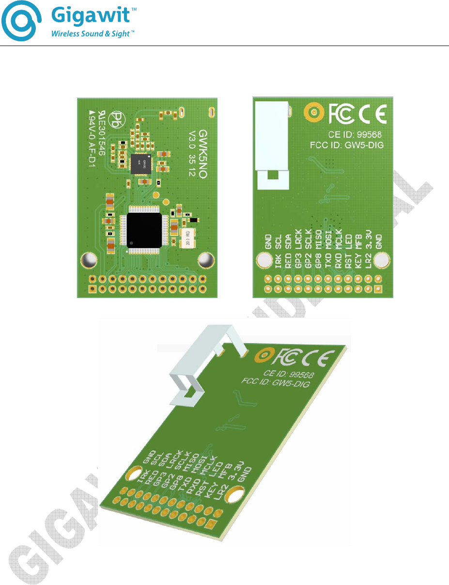
4. GWK5Nx Form Factor
©2008-2011 Gigawit Electronics Ltd. Version 1.0 Page 3 of 17
GWK5Nx Datasheet
5. Electrical Specification
Table [1]: Electrical Specification
Description Typical
Operation voltage +3.3V DC
Supply current TX: 60mA RX: 60mA (GWK5NO)
TX: 69mA RX: 63mA (GWK5NQ)
General
Operation temperature -10 ~ +60℃
RF Frequency 2400 ~ 2483MHZ
Modulation GFSK
Data rate 2M bps
TX Power +0dBm (GWK5NO)
+10dBm (GWK5NQ)
RX Sensitivity -90dBm (GWK5NO)
-88dBm (GWK5NQ)
RF
RF Range (indoor) 10m (GWK5NO)
15m (GWK5NQ)
Frequency Response 20~20KHz
S/N >85dB @ 20~20KHz
THD+N < 0.01% @ 20~20KHz
Dynamic range 80dB
Digital Audio Format I2S, Left Justify, Right Justify
Sample Rate Support 32KHz, 44.1KHz, 48KHz
Audio
Latency Fixed 15ms or application dependent
©2008-2011 Gigawit Electronics Ltd. Version 1.0 Page 4 of 17
GWK5Nx Datasheet
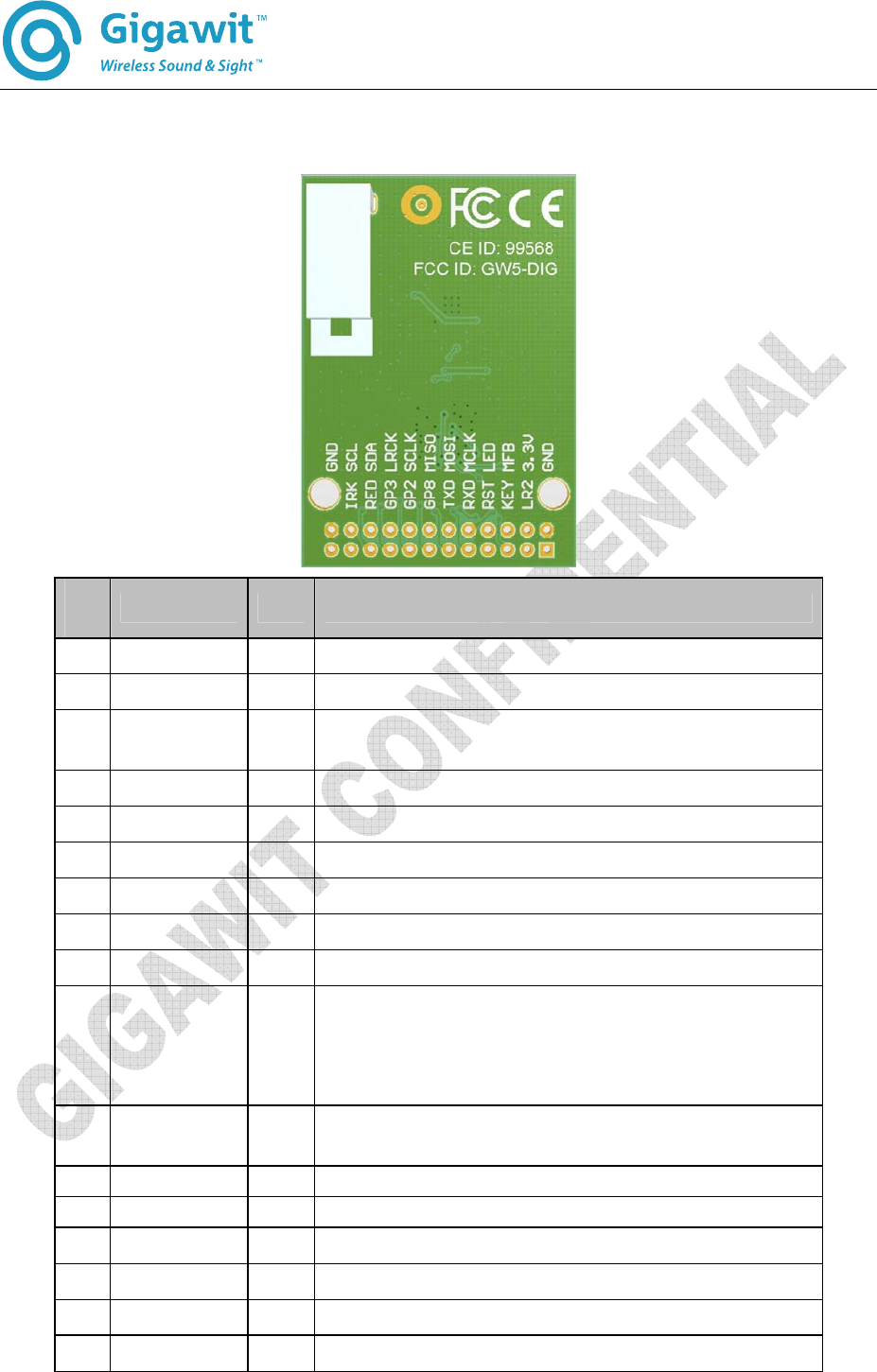
6. GWK5Nx Pin Assignment
Pin
# Pin name Type Description
1 GND P Ground
2 3.3V P +3.3V Power Input
3 MFB I/O Power or pairing key input, press long than 3s to turn on or
off the module, press long than 10s to enter pairing mode.
4 LED I/O Status LED output
5 MCLK O I2S Master Clock Output, NC when I2S is in slave mode
6 I2SMOSI I/O I2S Data Master Output / Slave Input
7 I2SMISO I/O I2S Data Master Input / Slave Output
8 SCLK I/O I2S Bit Clock Input / Output
9 LRCK I/O I2S Left and Right Clock Input / Output
10 SDA
/STANDBY
I/O I2C Data or Standby Control, firmware configurable. For
Standby mode, A high level will be asserted when no TX
signal >5s. When used as I2C, External 4.7K pull-up
resister required.
11 SCL
/MUTE
I/O I2C Clock or MUTE Control, firmware configurable.
When used as I2C, External 4.7K pull-up resister required.
12 GND P Ground
13 NC NA Not Connected
14 GP5 P General purpose IO
15 GP4 I/O General purpose IO
16 GP3 I/O General purpose IO
17 GP2 I/O General purpose IO
©2008-2011 Gigawit Electronics Ltd. Version 1.0 Page 5 of 17
GWK5Nx Datasheet
18 GP8 I/O General purpose IO
19 TXD I/O UART TX
20 RXD I/O UART RX
21 RST I Reset input, active low
22 KEY I/O Built-in ADC for KEY
23 LR2 I 192 KHz sampling rate LRCK input
24 NC NA Not Connected
Table [2]. GWK5Nx Pin Description
©2008-2011 Gigawit Electronics Ltd. Version 1.0 Page 6 of 17
GWK5Nx Datasheet
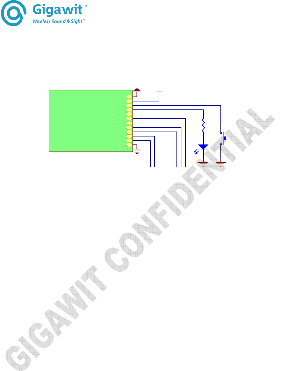
7. Application Schematic
R1
2K
LRCK
SCLK
SDIN
SDA
SCL
To DSP I2S Output
GND
3.3VIN
MFB
LED
SCL
SDA
MOSI
SCLK
MCLK
LRCK
GND
MISO
GWK5Nx
KEY
D1
LED
+3. 3V
To MCU I2C Control
Figure [1]: GWK5Nx Interfacing with DSP (I2S Slave Input Mode)
©2008-2011 Gigawit Electronics Ltd. Version 1.0 Page 7 of 17
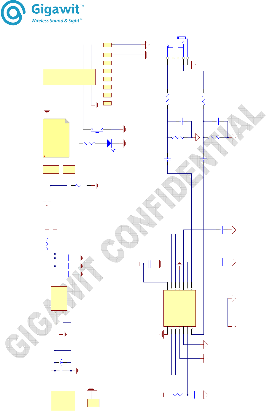
GWK5Nx Datasheet
I2SMCLK
I2SLRCK
I2SSCLK
I2SSDIN
BLED
SDA
SCL
MFB
1
2
3
4
5
6
7
8
9
10
11
12
13
14
15
16
17
18
19
20
21
22
23
24
J1
GWK5Nx
Vin
1
GND
2
ON/OFF
3
Vout 5
NC 4
U2
RT9193 C6
0.1uF/X7R
C4
10uF/10V/X7R
+5V
VCC33
R10
1.5K
BLUE
D1
MFB
SW1
R11
4.7K
1
2J2
Shunt for ISP
R1
0R 3.3VIN
3.3VIN
LCH
RCH
C12
1000pF/NPO
C9
1000pF/NPO
C8
10uF/10V/X7R
C11
10uF/10V/X7R
I2SLRCK
I2SMCLK
C14
10uF/10V/X7R
VCC33
C7
0.1uF/X7R
DVDD 1
SDATO 2
BCLK 3
FMT 4
CAP 5
VREF 6
RIN 7
LIN
8AVDD
9AGND
10 NOHP
11 LRCK
12 MLCK
13 DGND
14 U3
WM8738
C13
10uF/10V/X7R
C10
10uF/10V/X7R
R4
10K
R6
10K
R5
470
R2
470
I2SSCLK
I2SSDIN J6
Line In
+1
D- 2
D+ 3
4
_5
USB
J5 RXD
TXD
1
2
J4
BAT
+5V
VA
+5V
R3
5R1
+C1
220uF
C5
0.1uF/X7R
TXD
RXD
ADCKEY
RSTN
GPIO8
GPIO2
GPIO3
GPIO5
GPIO4
1
2
3
J3
C2
0.1uF/X7R
NC
NC
NC
NC
TP
1
TP
1
LCH
RCH
TP
1
TP
1
TP
1
TP
1
TP
1
I2SSCLK
I2SLRCK
I2SMCLK
TP
1
I2SSDIN
IfGWK5NxTXI2S
interfaceworkasslave
mode,usetheJ1pin19
asI2SSDIN,and
I2SMCLKremoved
Figure [2]: GWK5Nx Interfacing with ADC
©2008-2011 Gigawit Electronics Ltd. Version 1.0 Page 8 of 17
GWK5Nx Datasheet
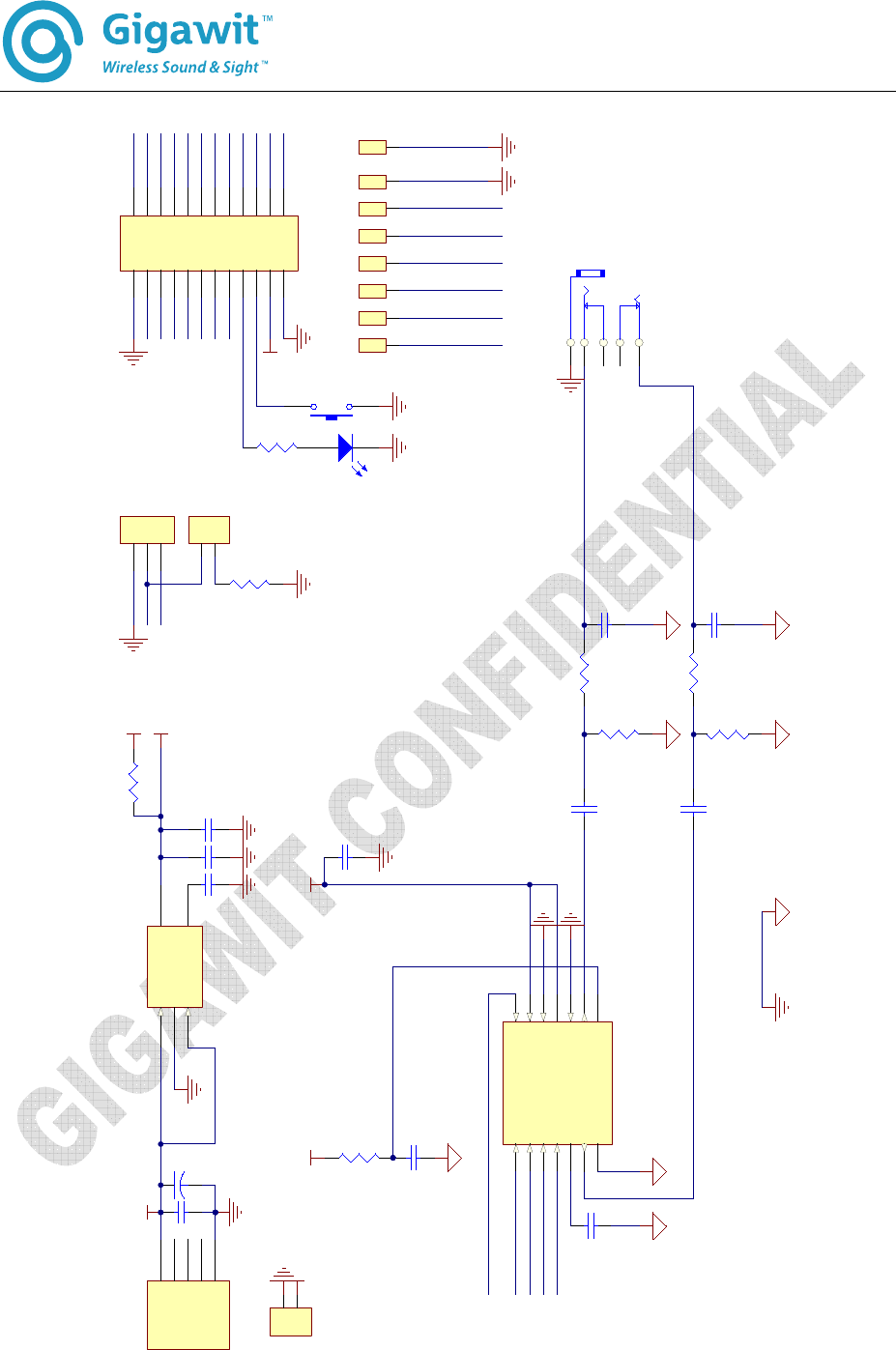
R3
470
R5
470
LCH
RCH
C16
2200pF/NPO
C14
2200pF/NPO
C13
10uF/10V/X7R
R6
10K
R4
10K
I2SSDOUT
I2SSCLK
I2SLRCK
I2SMCLK
LRCIN
1
DIN
2
BCKIN
3
ENABLE
4
CAP
5
VOUTR
6
GND
7VDD 8
VOUTL 9
MUTE 10
DVDD 11
DEEMPH 12
FORMAT 13
MCLK 14
U4
WM8501
VCC33
C8
10uF/10V/X7R
C6
0.1uF/X7R
DAC_EN
R2
5R1
+5V
C12
10uF/10V/X7R
C15
10uF/10V/X7R
J6
Line out
TP
1
TP
1
LCH
RCH
TP
1
TP
1
TP
1
TP
1
TP
1
I2SSCLK
R10
1.5K
BLUE
D1 MFB
SW1
VA
I2SSDOUT
I2SLRCK
I2SMCLK
I2SSCLK
I2SLRCK
I2SMCLK
TXD
RXD
BLED
SDA
SCL ADCKEY
3.3VIN
RSTN
MFB
GPIO8
1
2
3
4
5
6
7
8
9
10
11
12
13
14
15
16
17
18
19
20
21
22
23
24
J1
GWK5Nx
GPIO2
GPIO3
GPIO5
GPIO4
TP
1
I2SSDOUT
DAC_EN
Vin
1
GND
2
ON/OFF
3
Vout 5
NC 4
U2
RT9193 C3
0.1uF/X7R
C4
10uF/10V/X7R
+5V
VCC33
R11
4.7K
1
2J2
Shunt for ISP
R1
0R 3.3VIN
+1
D- 2
D+ 3
4
_5
USB
J5 RXD
TXD
1
2
J4
BAT
+5V
+C1
220uF
C5
0.1uF/X7R
1
2
3
J3
C2
0.1uF/X7R
NC
NC
NC
Figure [3]: GWK5Nx Interfacing with DAC
©2008-2011 Gigawit Electronics Ltd. Version 1.0 Page 9 of 17
GWK5Nx Datasheet
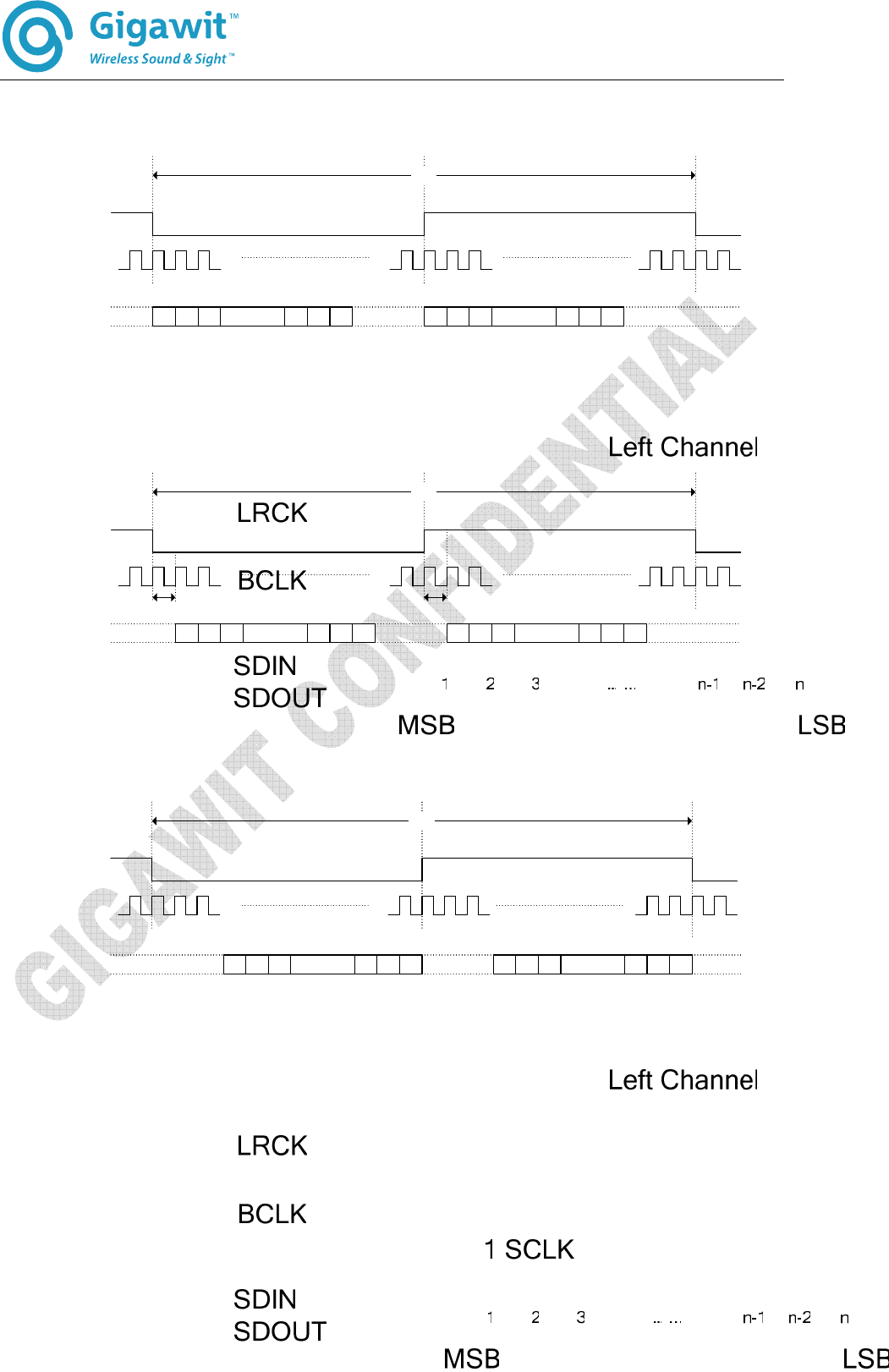
8. I2S Digital Audio Interface
GWK5Nx supports 3 digital audio interface modes: Left justify mode, I2S mode and Right justify mode.
Figure [4]. Left Justify Mode
Figure [5]. I2S Mode
Figure [6]. Right Justify Mode
©2008-2011 Gigawit Electronics Ltd. Version 1.0 Page 10 of 17
GWK5Nx Datasheet
GWK5Nx I2S interface can work as master or slave mode, the IO pin function is described below. The
default configuration is GWK5Nx Tx in I2S slave mode, and GWK5Nx RX in left justify master mode.
Other configurations are available upon customer request.
Master Mode Slave Mode
MCLK Output, Driving the external DSP or
Codec
Non function, can be left open
BCLK Output, Driving the external DSP or
Codec
Input, Driven by the external DSP or
Codec
LRCK Output, Driving the external DSP or
Codec
Input, Driven by the external DSP or
Codec
SDIN PCM Data Input PCM Data Input
SDOUT PCM Data Output PCM Data Output
Table [3]: GWK5Nx I2S Interface
©2008-2011 Gigawit Electronics Ltd. Version 1.0 Page 11 of 17
GWK5Nx Datasheet
9. I2C Control Interface
GWK5Nx features a standard I2C Control interface. The I2C can work as a master or a slave,
It can be used to control the peripheral devices or be controlled by the external MCU / DSP.
GWK5Nx features a two way wireless logical data channel; The I2C can also be used to exchange the
control information between the TX and RX side.
I2C Address is 0x0e, it is configurable by firmware.
Register Bit R/W Reset Description
0:
Mute
R/W 0 0: Mute off
1: Mute on
1:
Power
R/W 1 0: Power Off
1: Power On
2;
Link Status
R 0 0: Not Linked
1: Linked
3:
Standby
R/W 0: Standby off
1: Standby on
4-5:
Pairing
R/W 0 Write 1 to Enter pairing mode
Read back:
0: Normal Mode
1: Pairing in progress, pairing will be timeout in 30
seconds.
2: Paired with success
3: Pairing failed, time is out
0x00:
Control
6-7:
Reserved
R/W 0
0x01:
Volume
0-7 R/W 0 Volume 0dB to -48dB
0x00: 0dB
0xd0: -48dB
0x02:
Treble
0-7 R/W 0 Treble -14dB to + 14dB
0xf2: -14dB
0x00: 0dB
0x0e: +14dB
0x03:
Bass
0-7 R/W 0 Bass -14dB to + 14dB
0xf2: -14dB
0x00: 0dB
0x0e: +14dB
0x04:
Balance
0-7 R/W 0 Balance -12dB to + 12dB
0xf4: -12dB
0x00: 0dB
0x0c: +12dB
Table [4] I2C Registers
©2008-2011 Gigawit Electronics Ltd. Version 1.0 Page 12 of 17
GWK5Nx Datasheet
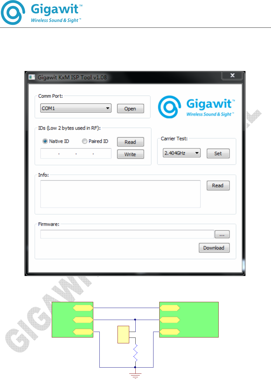
10. ISP Firmware Updating
GWK5Nx support ISP firmware updating through UART, When TXD pin connected with a 4.7K resistor to
the GND, GWK5Nx will enter the ISP mode.
Figure [7]: Gigawit ISP tool
R1
4.7K
USB to UART
TXD
RXD
GND
J1
Short for ISP
GWK5 Module
TXD
RXD
GND
Figure [8]: Gigawit ISP Connection
©2008-2011 Gigawit Electronics Ltd. Version 1.0 Page 13 of 17
GWK5Nx Datasheet
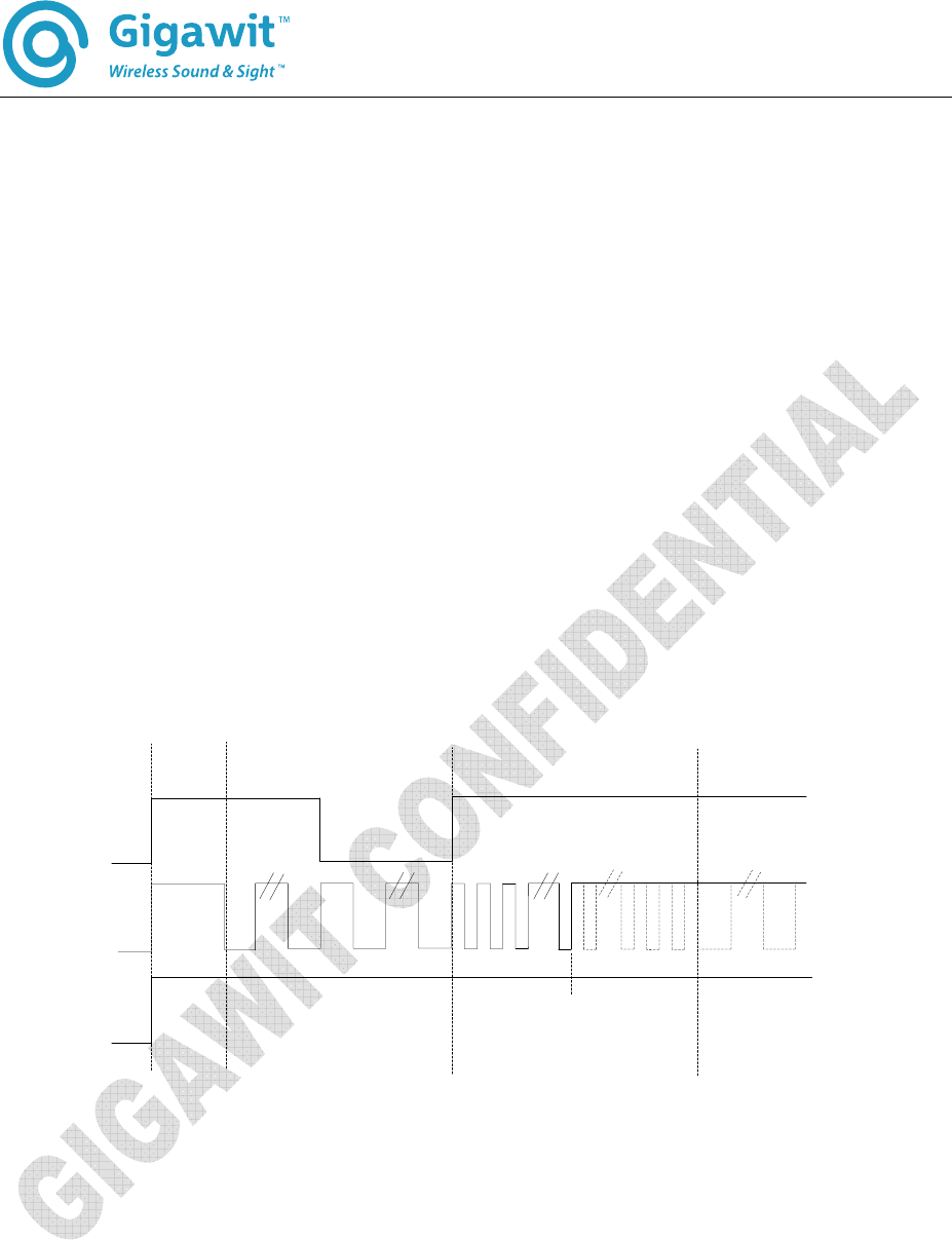
11. Pairing
GWK5Nx support ID matching to enable multi TX/RX operating in a same area. The RX will only receive
the paired TX audio signals. To pair the TX and RX module, follow the below steps:
1) Power on the TX and RX Module. The TX/RX LED will keep solid for 5 seconds, and then turn into
Idle Mode and flash slowly.
2) Press the TX key long than 10 seconds Until the LED change into flashing fast. Release the key.
After this, The TX Module will stay into Pairing Mode for 30 seconds until it find the RX (the RX must
be in Pairing Mode in 30 seconds, see Step 3).If the TX found the RX in 30 seconds and paired, the
LED will turn to solid and quit the Pairing Mode, or it will be time out after 30 seconds and turn the
Pairing Mode into the Idle Mode.
3) Press the RX key long than 10 seconds Until the LED change into flashing fast. Release the key.
After this, The RX Module will stay into Pairing Mode for 30 seconds until it find the TX (the TX must
be in Pairing Mode, see Step 2) If the RX found the RX in 30 seconds and paired, the LED will turn
to solid and quit the Pairing Mode, or it will be time out after 30 seconds and turn the Pairing Mode
into the Idle Mode.
4) When the TX and the RX are paired, The TX/RX LED will stay in solid .the RX can receive the TX
signal.
Figure [9]: Key and LED Timing at pairing mode
©2008-2011 Gigawit Electronics Ltd. Version 1.0 Page 14 of 17
GWK5Nx Datasheet
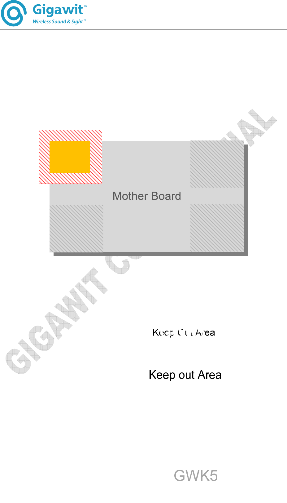
12. Mounting Requirements
GWK5Nx is a sensitive RF part. Need to mount them at the corner of the mother circuit board and
reserve some keep out space to the components on the mother board. Try to keep them away with metal
components like Speakers, Transformers, Batteries, Big Aluminum Capacitors, Heat Sinks and Metal
Panels.
The figure below illustrates how to mount the GWK5 module. Improper mounting will decrease the RF
performance dramatically.
Figure [10]: GWK5Nx Mounting Rule
©2008-2011 Gigawit Electronics Ltd. Version 1.0 Page 15 of 17
GWK5Nx Datasheet
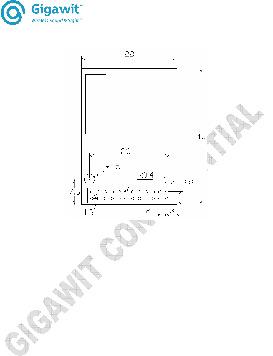
13. GWK5Nx Physical Dimension
Figure [11]: GWK5Nx Dimension
©2008-2011 Gigawit Electronics Ltd. Version 1.0 Page 16 of 17
GWK5Nx Datasheet
14. Naming Rule
Gigawit Products Prefix
Wireless Audio K5 Family
N Module
RF Power Varaint
O:0dBm, without PA

©2008-2011 Gigawit Electronics Ltd. Version 1.0 Page 17 of 17
GWK5Nx Datasheet
15. Ordering Information
Gigawit ID. Description
GWK5NO 0dBm RF Power module
16. Contact
捷电科技有限公司 Gigawit Electronics Limited
512 Building R2-A, Virtual University ,Science Park,
Nanshan District, 518057 Shenzhen, China
Tel:+86-755-86329300, Fax:+86-755-86329882
http://www.gigawit.com
17. Revision History
2011-8-22 Version 1.0, Original version