Gilbarco MRIR8 Drive-Thru Reader Radio Identification Device User Manual Manual
Gilbarco Inc. Drive-Thru Reader Radio Identification Device Manual
UserManual.wiki
>
Gilbarco
>
MRIR8 User Manual
Manual
Navigation menu
Upload a User Manual
Namespaces
Wiki Guide
HTML
PDF
Info
Views
User Manual
Discussion / Help
Navigation
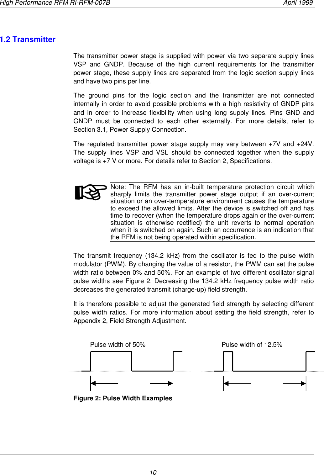
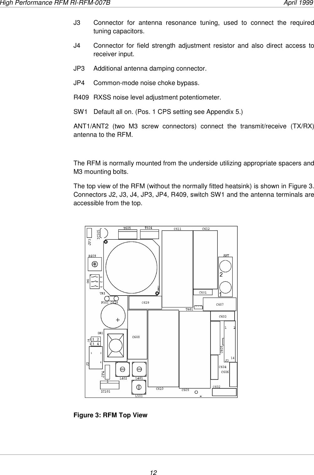
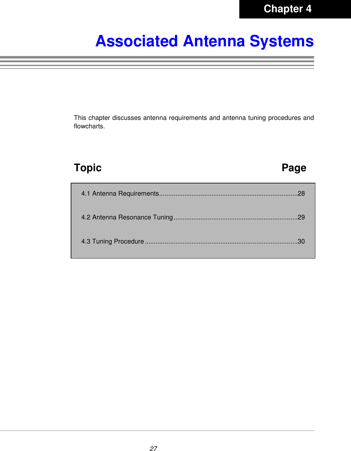
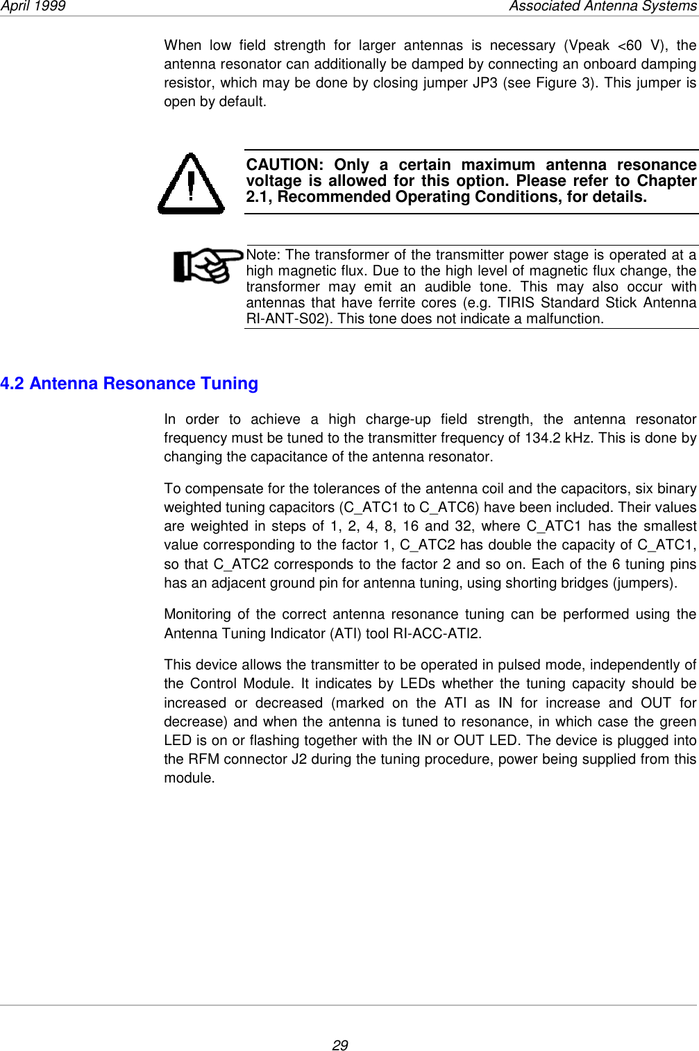
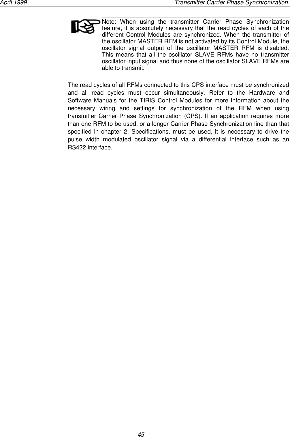
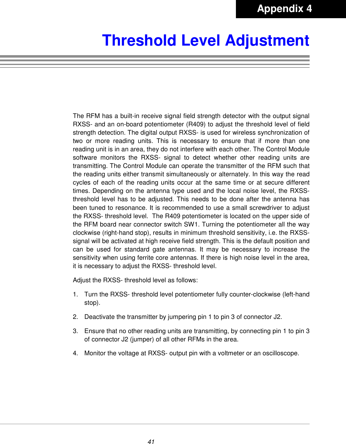
![High Performance RFM RI-RFM-007B April 199940Table 14: Oscillator Signal Pulse Width versus Resistor Value (estimatedvalues)Resistor value[kΩΩΩΩ]Oscillator signalpulse width [%] Field strengthreduction [dB]open 50 0151 37 -359 25 -617 12 -1210 6 -18shorted 0 ∞CAUTION: When using pulse widths smaller than 50%, theRFM transmitter power stage works less efficiently. Thisleads to an increased power dissipation and thus to ahigher temperature of the transmitter power stage. Ensurethat the antenna resonance voltage does not exceed 200Vp when the selected oscillator signal pulse width settingis smaller than 25%.Note: The pulse width for an oscillator signal pulse width setting of 5%and smaller is extremely short. The pulse response of the RFMtransmitter power stage to this short pulse is different for each unit. Inorder to have reproducible field strength values for different RFMs, it isnot recommended to use the smallest pulse width setting.](https://usermanual.wiki/Gilbarco/MRIR8/User-Guide-147838-Page-40.png)
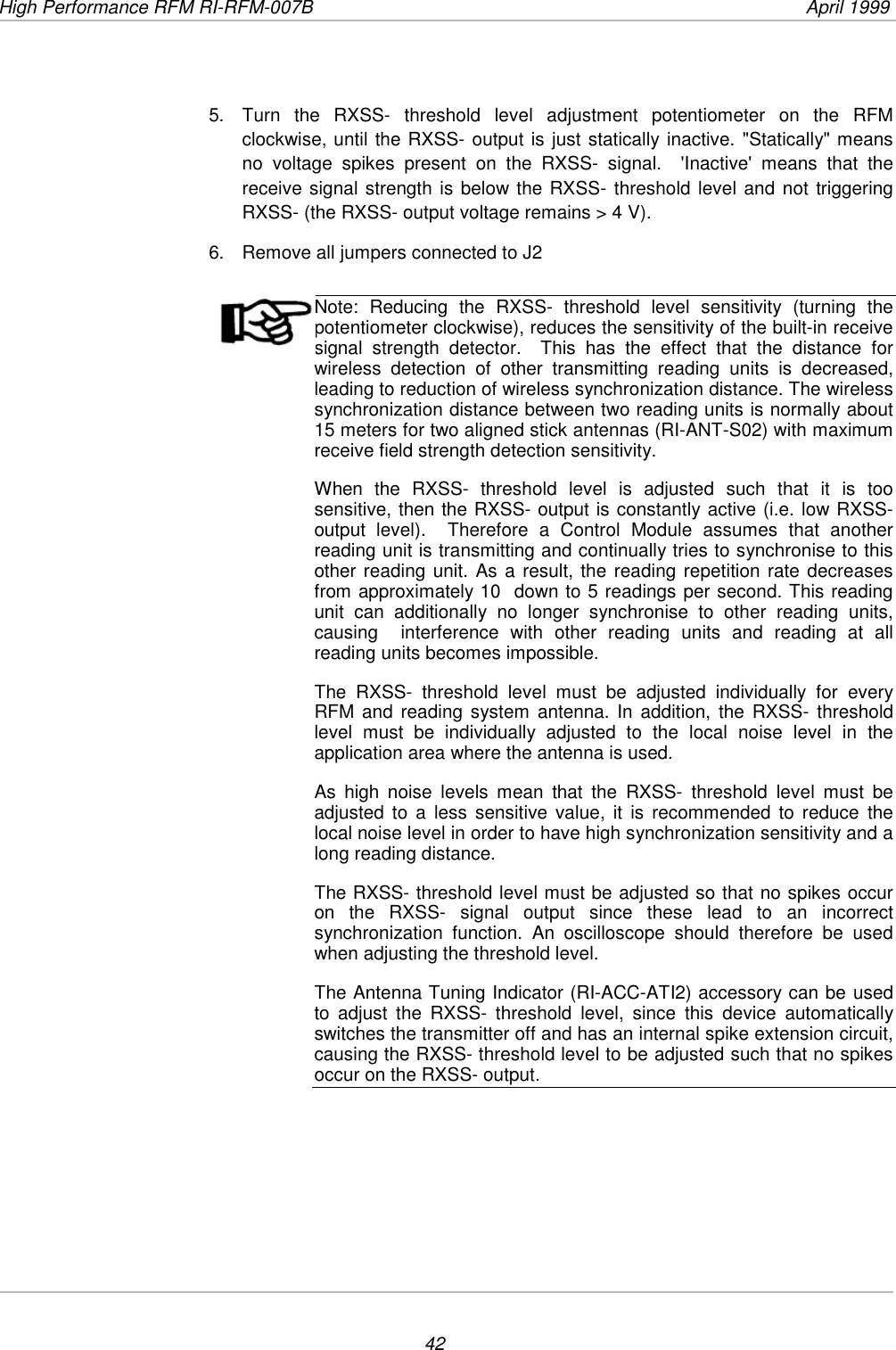
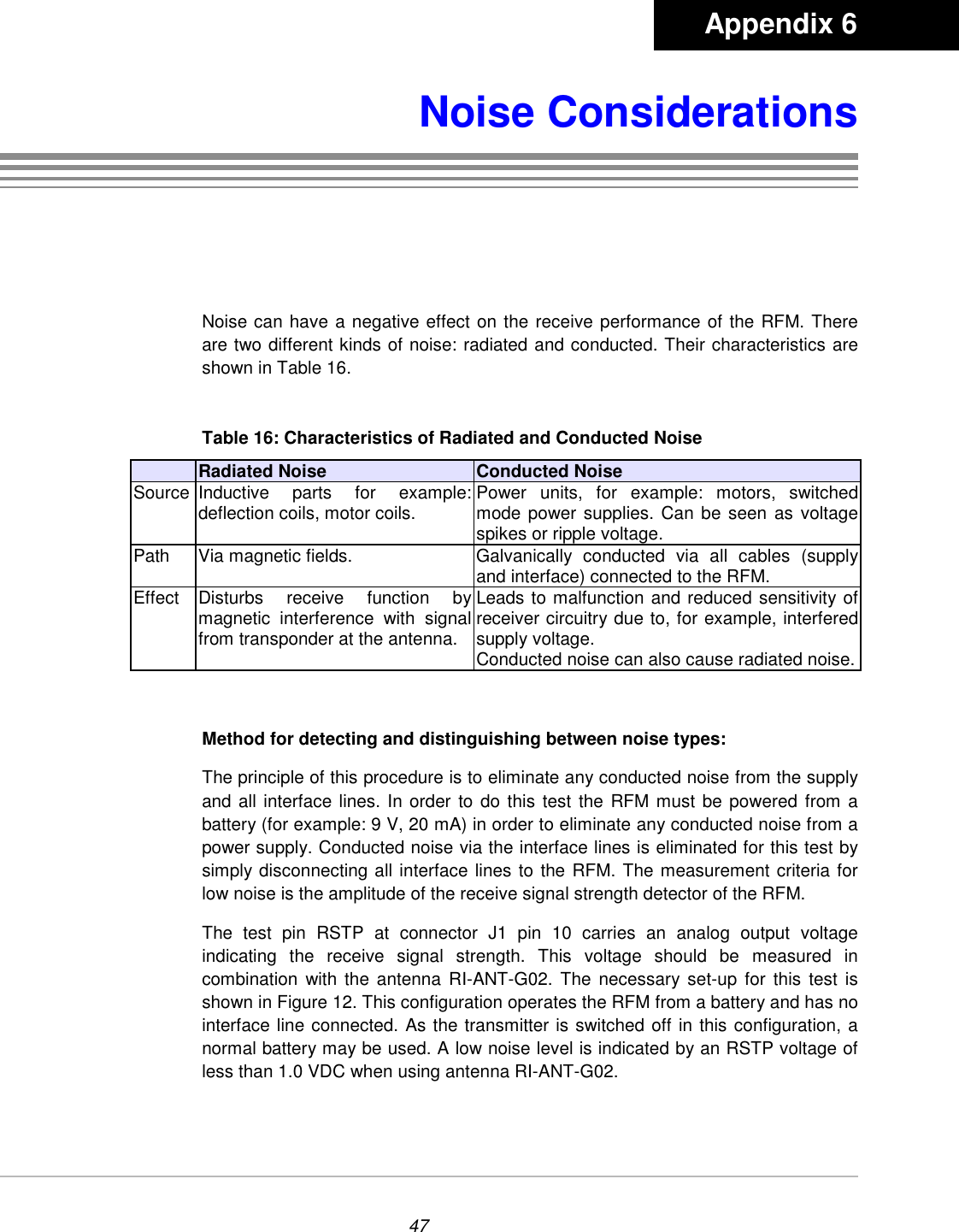
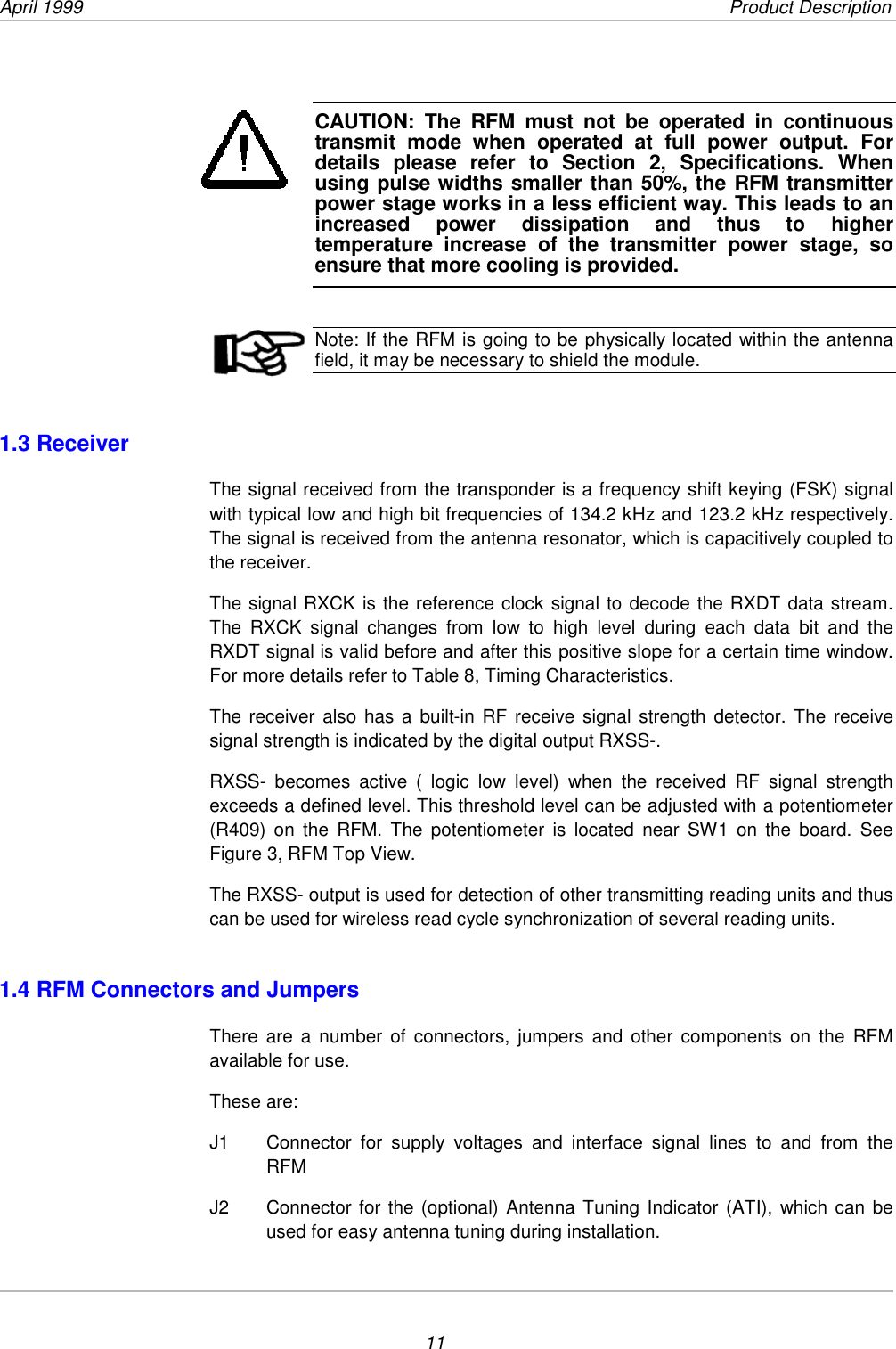
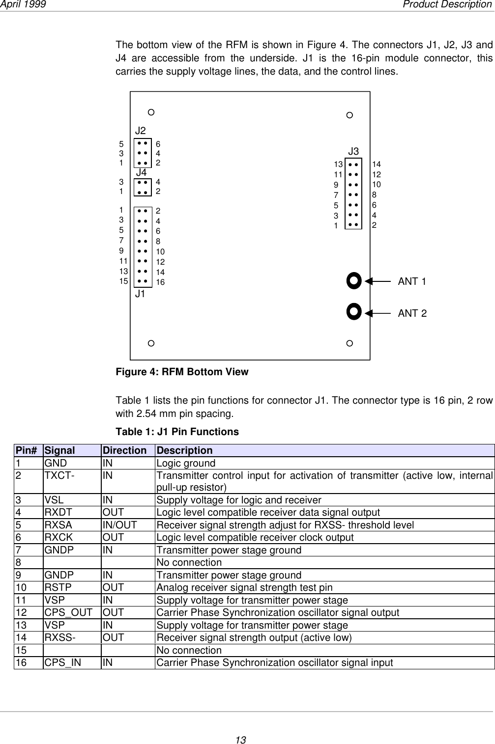
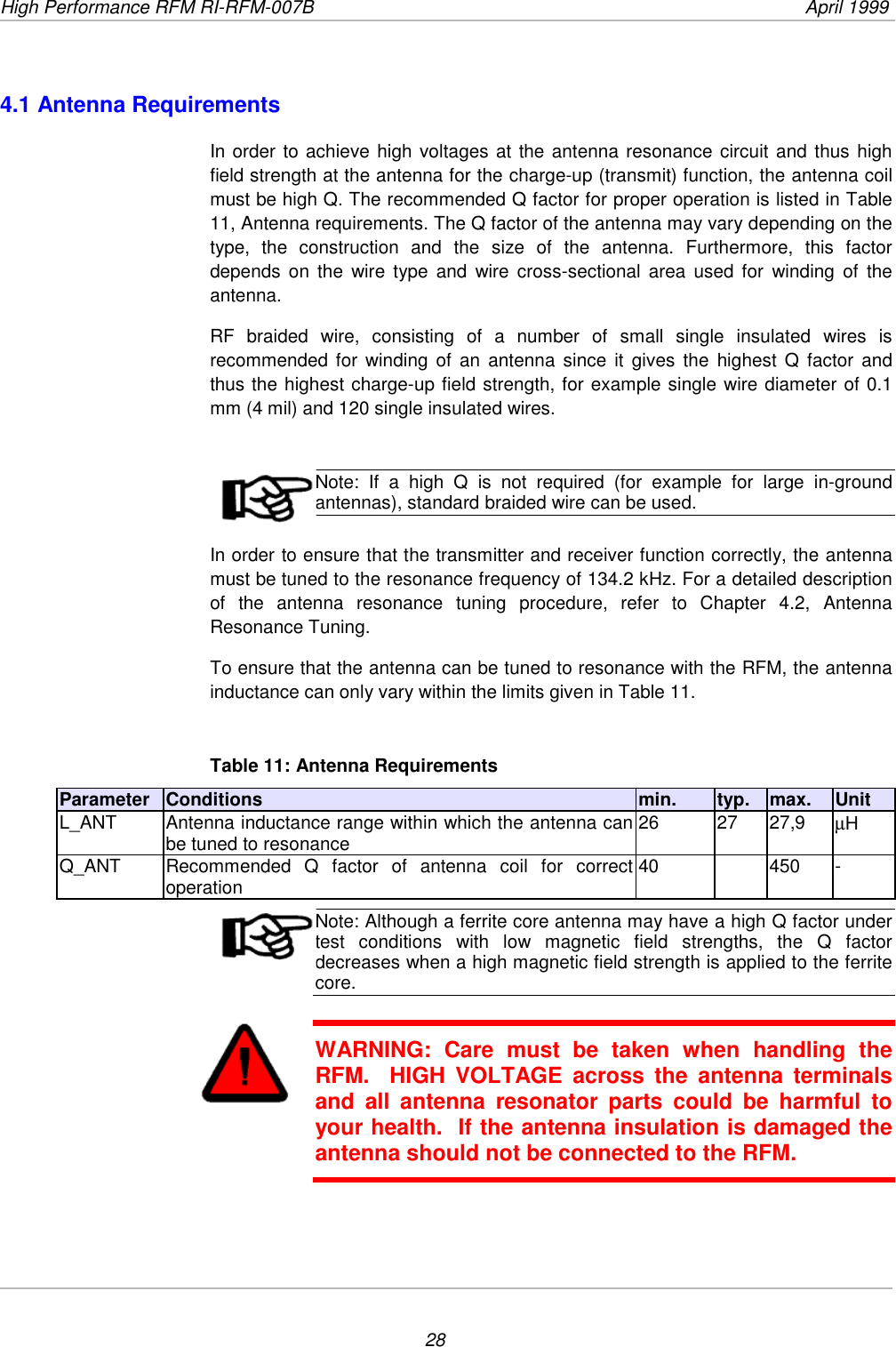
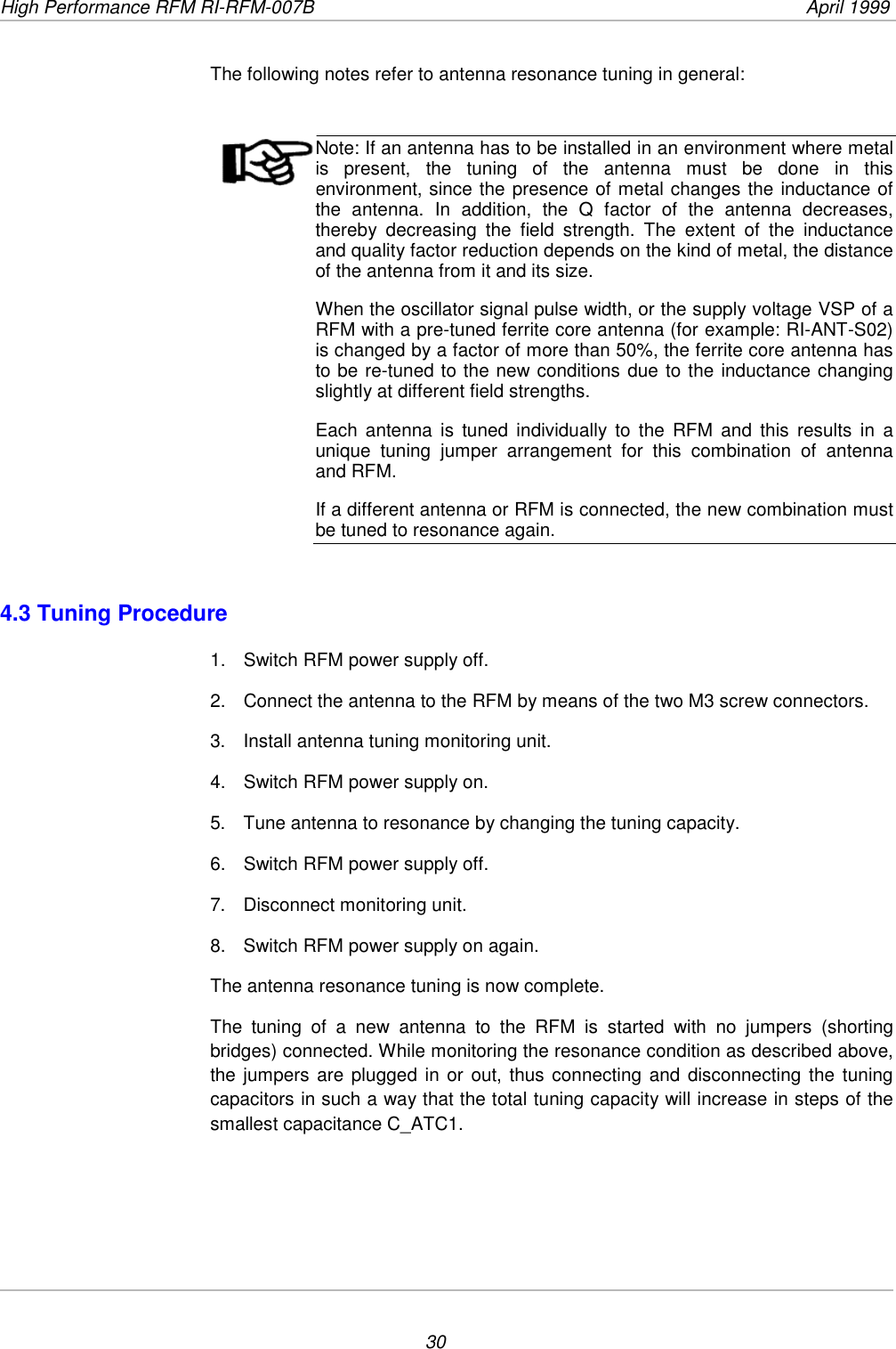
![High Performance RFM RI-RFM-007B April 199944If several antennas are used close to each other, a check should be made todetermine if the charge-up field strength changes regularly (i.e. beat effect ). Thismay be checked by verifying the antenna resonance voltage with an oscilloscope.If the antenna resonator voltage changes periodically by more than approximately5% of the full amplitude it is appropriate to use wired transmitter carrier phasesynchronization.In addition, the distances given in Table 15 can be used as a guideline todetermine when it is necessary to cross-check for beat effect. If these distancesare less than the value given in Table 15, a check for beat effect should be made.The values given refer to the distances shown in Figure 11 and are valid formaximum charge-up field strength.Figure 11: Distance between Antennas (top view)Table 15: Maximum Distances between AntennasAntenna type Distance D1 [m] Distance D2 [m]RI_ANT_S02 <=> RI_ANT_S02 0,8 1,0RI_ANT_G01 <=> RI_ANT_G01 1.7 1.5RI_ANT_G02 <=> RI_ANT_G02 1.3 1.0RI_ANT_G04 <=> RI_ANT_G04 2.0 1.7This effect will not occur if the transmitters of different RFMs are operated from thesame oscillator signal. This is the reason why the pulse width modulated oscillatorsignal is accessible at the connector J1.ConfigurationMaster or Slave setting of a RFM is determined by switch 1 position 1 (SW1/1). Ifthis is in the ON position, the RFM is a MASTER, if in the OFF position, it is aSLAVE. When a RFM has been configured as a master, then J1 pin 12 of this unitshould be connected to J1 pin 16 of the slave units to allow the master oscillatoroutput (CPS_OUT) to drive the slave oscillator inputs (CPS_IN). The logic ground(e.g. J1 pin 1) of both master and slave units should be connected together.Caution: Use overvoltage protection components at theCPS connector for CPS lines between 0.5m and 5m.Distance D1Antenna 1 Antenna 2Distance D2Antenna 1 Antenna 2](https://usermanual.wiki/Gilbarco/MRIR8/User-Guide-147838-Page-44.png)