Gilbarco MRIR8 Drive-Thru Reader Radio Identification Device User Manual Manual
Gilbarco Inc. Drive-Thru Reader Radio Identification Device Manual
Gilbarco >
Manual

1
Series 2000 Reader System
High Performance RFM RI-RFM-007B
Reference Guide
11-06-21-042 April 1999
High Performance RFM RI-RFM-007B April 1999
2
Second Edition - April 1999
This manual describes the TIRIS High Performance RFM RI-RFM-007B,
hereafter referred to as the RFM.
Important Notice
Texas Instruments reserves the right to change its products or services or to
discontinue any product or service at any time without notice. TI provides customer
assistance in various technical areas, but does not have full access to data
concerning the use and applications of customer's products.
Therefore, TI assumes no liability and is not responsible for customer applications
or product or software design or performance relating to systems or applications
incorporating TI products. In addition, TI assumes no liability and is not responsible
for infringement of patents and/or any other intellectual or industrial property rights
of third parties, which may result from assistance provided by TI.
TI products are not designed, intended, authorized or warranted to be suitable for
life support applications or any other life critical applications which could involve
potential risk of death, personal injury or severe property or environmental damage.
The TIRIS logo and the word TIRIS are registered trademarks of Texas
Instruments Incorporated.
Copyright 1998 Texas Instruments Incorporated. All rights reserved.

April 1999 Contents
3
Table of Contents
Preface.................................................................................................................5
Chapter 1: Product Description ........................................................................7
1.1 General.......................................................................................................8
1.2 Transmitter ...............................................................................................10
1.3 Receiver ...................................................................................................11
1.4 RFM Connectors and Jumpers ................................................................11
Chapter 2: Specifications ................................................................................17
2.1 Recommended Operating Conditions ......................................................18
2.2 Dimensions...............................................................................................22
Chapter 3: Installation......................................................................................23
3.1 Power Supply Requirements....................................................................24
3.2 Power Supply Connection ........................................................................25
Chapter 4: Associated Antenna Systems ......................................................27
4.1 Antenna Requirements.............................................................................28
4.2 Antenna Resonance Tuning.....................................................................29
4.3 Tuning Procedure.....................................................................................30
Appendices
Appendix 1: Expanding Antenna Tuning Inductance Range..........................33
Appendix 2: Field Strength Adjustment..........................................................37
Appendix 3: Adjustment of Oscillator Signal Pulse Width..............................39
Appendix 4: Threshold Level Adjustment.......................................................41
Appendix 5: Transmitter Carrier Phase Synchronization (CPS) ....................43
Appendix 6: Noise Considerations .................................................................47
Appendix 7: Over Voltage Protection .............................................................49

High Performance RFM RI-RFM-007B April 1999
4
Table Locations
Table 1: J1 Pin Functions ................................................................................................................................ 13
Table 2: J2 Pin Functions ................................................................................................................................ 14
Table 3: J4 Pin Functions ................................................................................................................................ 14
Table 4: J3 Pin Functions ................................................................................................................................ 15
Table 5: Antenna Connectors.......................................................................................................................... 15
Table 6: Operating Conditions......................................................................................................................... 18
Table 7: Electrical Characteristics ................................................................................................................... 20
Table 8: Timing Characteristics ....................................................................................................................... 21
Table 9: Mechanical Parameters..................................................................................................................... 21
Table 10: Power Supply Ripple Specifications................................................................................................ 24
Table 11: Antenna Requirements.................................................................................................................... 28
Table 12: Capacitor Values for Expanding Antenna Tuning Range to Lower Values..................................... 34
Table 13: Capacitor Values Expanding Antenna Tuning Range to Higher Values ......................................... 35
Table 14: Oscillator Signal Pulse Width versus Resistor Value (estimated values)........................................ 40
Table 15: Maximum Distances between Antennas ......................................................................................... 44
Table 16: Characteristics of Radiated and Conducted Noise.......................................................................... 47
Figure Locations
Figure 1: RFM Block Schematic........................................................................................................................ 8
Figure 2: Pulse Width Examples ..................................................................................................................... 10
Figure 3: RFM Top View.................................................................................................................................. 12
Figure 4: RFM Bottom View............................................................................................................................. 13
Figure 5: Mechanical Dimensions ................................................................................................................... 22
Figure 6: External Ground Connection (GND to GNDP)................................................................................. 26
Figure 7: Tuning Example showing Increase of Total Tuning Capacity.......................................................... 31
Figure 8: Flow-chart for Tuning the Antenna to Resonance............................................................................ 32
Figure 9: Circuit for Expanding Antenna Tuning Range to Lower Values....................................................... 34
Figure 10: Circuit for Expanding Antenna Tuning Range to Higher Values.................................................... 35
Figure 11: Distance between Antennas (top view).......................................................................................... 44
Figure 12: Noise Testing Configuration........................................................................................................... 48
Figure 13: Circuit for Overvoltage Protection .................................................................................................. 50

5
FCC/PTT Regulations
The TIRIS RFM generates RF emissions at 134.2 kHz. The radiation of the
fundamental and harmonics will vary with the type of antenna and other devices or
functions connected to the RFM.
Prior to operating the RFM together with antenna(s), power supply and a control
module or other devices, the required FCC, PTT or relevant government agency
approvals must be obtained.
Sale, lease or operation in some countries may be subject to prior approval by
governmental and other organizations or agencies.
CE Conformity
A CE Declaration of Conformity is available for this module in a typical
configuration. Any device or system incorporating this module in any other than the
original CE configuration needs to be verified against the European EMC directive.
A separate Declaration of Conformity must be issued by the system integrator or
user of such a system prior to marketing it and operating it in the European
Community.
Preface
High Performance RFM RI-RFM-007B April 1999
6
Conventions
Certain conventions are used in order to display important information in this
manual, these conventions are:
WARNING: A warning is used where care must be
taken, or a certain procedure must be followed, in
order to prevent injury or harm to your health.
CAUTION: This indicates information on conditions which
must be met, or a procedure which must be followed,
which if not heeded could cause permanent damage to the
RFM.
Note: Indicates conditions which must be met, or procedures which
must be followed, to ensure proper functioning of the RFM.

7
Product Description
This chapter introduces the RFM component assemblies, showing the transmitter
and receiver sections and placement of key user-accessible components.
Topic Page
1.1 General.......................................................................................................8
1.2 Transmitter ...............................................................................................10
1.3 Receiver ...................................................................................................11
1.4 RFM Connections and Jumpers...............................................................11
Chapter 1
High Performance RFM RI-RFM-007B April 1999
8
1.1 General
WARNING: Care must be taken when handling the
RFM. High voltage across the antenna terminals, all
antenna components and some parts of the printed
circuit board (PCB) could be harmful to your health. If
the antenna insulation is damaged, the antenna
should not be connected to the RFM.
CAUTION: This product may be subject to damage by
electrostatic discharge (ESD). It should be handled by ESD
protected personnel at ESD secured workplaces only. The
transmitter power output stage can only operate with a
limited duty cycle. Please pay attention to this whilst
performing antenna tuning procedures. Ground pins GND
and GNDP must be connected externally to avoid damage
to the unit.
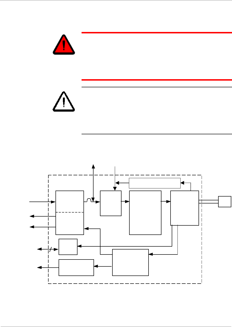
The RFM is an integral part of the TIRIS system. Coupled with a Control Module
and an antenna, it is used for wireless identification of TIRIS transponders. A block
schematic is shown in Figure 1.
Figure 1: RFM Block Schematic
PWM
TX
Oscillator
RX
demodulator
RXSS-
Interface
Antenna
Circuit TX/RX
Antenna
RX
Amplif ier
RXSS
threshold
ATI
Int.
TX Power
Stage
CPS
TXCT-
RXDT
RXCK
ATI 6
Threshold
Demodulator
PWM Control Input
Overvoltage Protection

April 1999 Product Description
9
The RFM contains all the analogue functions of a TIRIS reading unit needed to
send an energizing signal via the antenna to initialize a TIRIS transponder, to
demodulate the received identification signal and to send the received data
together with clock signals to a Control Module.
The RFM also sends the necessary programming and addressing signals to
Read/Write and Multipage transponders.
The data input and output lines, which are connected to a data processing unit, are
low-power Schottky TTL and HCMOS logic compatible.
The functions of the RFM are described in the following section.
High Performance RFM RI-RFM-007B April 1999
10
1.2 Transmitter
The transmitter power stage is supplied with power via two separate supply lines
VSP and GNDP. Because of the high current requirements for the transmitter
power stage, these supply lines are separated from the logic section supply lines
and have two pins per line.
The ground pins for the logic section and the transmitter are not connected
internally in order to avoid possible problems with a high resistivity of GNDP pins
and in order to increase flexibility when using long supply lines. Pins GND and
GNDP must be connected to each other externally. For more details, refer to
Section 3.1, Power Supply Connection.
The regulated transmitter power stage supply may vary between +7V and +24V.
The supply lines VSP and VSL should be connected together when the supply
voltage is +7 V or more. For details refer to Section 2, Specifications.
Note: The RFM has an in-built temperature protection circuit which
sharply limits the transmitter power stage output if an over-current
situation or an over-temperature environment causes the temperature
to exceed the allowed limits. After the device is switched off and has
time to recover (when the temperature drops again or the over-current
situation is otherwise rectified) the unit reverts to normal operation
when it is switched on again. Such an occurrence is an indication that
the RFM is not being operated within specification.
The transmit frequency (134.2 kHz) from the oscillator is fed to the pulse width
modulator (PWM). By changing the value of a resistor, the PWM can set the pulse
width ratio between 0% and 50%. For an example of two different oscillator signal
pulse widths see Figure 2. Decreasing the 134.2 kHz frequency pulse width ratio
decreases the generated transmit (charge-up) field strength.
It is therefore possible to adjust the generated field strength by selecting different
pulse width ratios. For more information about setting the field strength, refer to
Appendix 2, Field Strength Adjustment.
Figure 2: Pulse Width Examples
Pulse width of 50% Pulse width of 12.5%

April 1999 Product Description
11
CAUTION: The RFM must not be operated in continuous
transmit mode when operated at full power output. For
details please refer to Section 2, Specifications. When
using pulse widths smaller than 50%, the RFM transmitter
power stage works in a less efficient way. This leads to an
increased power dissipation and thus to higher
temperature increase of the transmitter power stage, so
ensure that more cooling is provided.
Note: If the RFM is going to be physically located within the antenna
field, it may be necessary to shield the module.
1.3 Receiver
The signal received from the transponder is a frequency shift keying (FSK) signal
with typical low and high bit frequencies of 134.2 kHz and 123.2 kHz respectively.
The signal is received from the antenna resonator, which is capacitively coupled to
the receiver.
The signal RXCK is the reference clock signal to decode the RXDT data stream.
The RXCK signal changes from low to high level during each data bit and the
RXDT signal is valid before and after this positive slope for a certain time window.
For more details refer to Table 8, Timing Characteristics.
The receiver also has a built-in RF receive signal strength detector. The receive
signal strength is indicated by the digital output RXSS-.
RXSS- becomes active ( logic low level) when the received RF signal strength
exceeds a defined level. This threshold level can be adjusted with a potentiometer
(R409) on the RFM. The potentiometer is located near SW1 on the board. See
Figure 3, RFM Top View.
The RXSS- output is used for detection of other transmitting reading units and thus
can be used for wireless read cycle synchronization of several reading units.
1.4 RFM Connectors and Jumpers
There are a number of connectors, jumpers and other components on the RFM
available for use.
These are:
J1 Connector for supply voltages and interface signal lines to and from the
RFM
J2 Connector for the (optional) Antenna Tuning Indicator (ATI), which can be
used for easy antenna tuning during installation.
High Performance RFM RI-RFM-007B April 1999
12
J3 Connector for antenna resonance tuning, used to connect the required
tuning capacitors.
J4 Connector for field strength adjustment resistor and also direct access to
receiver input.
JP3 Additional antenna damping connector.
JP4 Common-mode noise choke bypass.
R409 RXSS noise level adjustment potentiometer.
SW1 Default all on. (Pos. 1 CPS setting see Appendix 5.)
ANT1/ANT2 (two M3 screw connectors) connect the transmit/receive (TX/RX)
antenna to the RFM.
The RFM is normally mounted from the underside utilizing appropriate spacers and
M3 mounting bolts.
The top view of the RFM (without the normally fitted heatsink) is shown in Figure 3.
Connectors J2, J3, J4, JP3, JP4, R409, switch SW1 and the antenna terminals are
accessible from the top.
Figure 3: RFM Top View
April 1999 Product Description
13
The bottom view of the RFM is shown in Figure 4. The connectors J1, J2, J3 and
J4 are accessible from the underside. J1 is the 16-pin module connector, this
carries the supply voltage lines, the data, and the control lines.
Figure 4: RFM Bottom View
Table 1 lists the pin functions for connector J1. The connector type is 16 pin, 2 row
with 2.54 mm pin spacing.
Table 1: J1 Pin Functions
Pin# Signal Direction Description
1 GND IN Logic ground
2 TXCT- IN Transmitter control input for activation of transmitter (active low, internal
pull-up resistor)
3 VSL IN Supply voltage for logic and receiver
4 RXDT OUT Logic level compatible receiver data signal output
5 RXSA IN/OUT Receiver signal strength adjust for RXSS- threshold level
6 RXCK OUT Logic level compatible receiver clock output
7 GNDP IN Transmitter power stage ground
8 No connection
9 GNDP IN Transmitter power stage ground
10 RSTP OUT Analog receiver signal strength test pin
11 VSP IN Supply voltage for transmitter power stage
12 CPS_OUT OUT Carrier Phase Synchronization oscillator signal output
13 VSP IN Supply voltage for transmitter power stage
14 RXSS- OUT Receiver signal strength output (active low)
15 No connection
16 CPS_IN IN Carrier Phase Synchronization oscillator signal input
ANT 1
ANT 2
5
3
1
3
1
1
3
5
7
9
11
13
15
• •
• •
• •
• •
• •
• •
• •
• •
• •
• •
• •
• •
• •
6
4
2
4
2
2
4
6
8
10
12
14
16
• •
• •
• •
• •
• •
• •
• •
J1
J2
J4
J3
14
12
10
8
6
4
2
13
11
9
7
5
3
1
High Performance RFM RI-RFM-007B April 1999
14
CAUTION: The transmitter ground pins GNDP and logic
ground pin GND must be connected together externally.
The RFM may be otherwise permanently damaged.
Table 2 lists the pin functions for the ATI connector J2: The connector type is a
6 pin, 2 row connector with 2.54 mm pin spacing.
Table 2: J2 Pin Functions
Pin# Signal Direction Description
1 TXCT-R IN Transmitter control signal via resistor (active low)
2 GND OUT Logic ground
3 VD OUT Internal regulated logic supply voltage output
4 F_OSC-R IN/OUT Pulse width modulated transmitter oscillator signal via resistor
5 RXSS- OUT Receiver signal strength output (active low)
6 F_ANT OUT Antenna resonance frequency output signal (open collector)
Table 3 lists the pin functions for the J4 pulse width adjustment connector. The
connector type is 4 pin, 2 row with 2.54 mm pin spacing.
Table 3: J4 Pin Functions
Pin# Signal Description
1 RX Analog transponder signal
2 GNDA Ground antenna circuit
3 Pulse width adjusting resistor
connecting pin
4 GND Logic ground
April 1999 Product Description
15
Table 4 lists the functions for connector J3. This is a 14 pin, 2 row connector with
2.54 mm pin spacing.
Table 4: J3 Pin Functions
Pin# Signal Description
1 ATC1 Antenna tuning capacitor 1 (weighted value 1)
2 GNDA Ground antenna circuit
3 ATC2 Antenna tuning capacitor 2 (weighted value 2)
4 GNDA Ground antenna circuit
5 ATC3 Antenna tuning capacitor 3 (weighted value 4)
6 GNDA Ground antenna circuit
7 ATC4 Antenna tuning capacitor 4 (weighted value 8)
8 GNDA Ground antenna circuit
9 ATC5 Antenna tuning capacitor 5 (weighted value 16)
10 GNDA Ground antenna circuit
11 ATC6 Antenna tuning capacitor 6 (weighted value 32)
12 GNDA Ground antenna circuit
13 AMTP Antenna circuit test point
14 No connection
Table 5 lists the pin functions for the antenna terminal connectors: Metric screws
size M3 are used for connection.
Table 5: Antenna Connectors
Signal Description
ANT1 Antenna resonator (capacitor side)
ANT2 Antenna resonator (transformer side)
Jumper JP4 allows enabling and disabling of common noise filtering for EMI
purposes. The default setting, with common noise filtering active, jumpers pins 2
and 3. A jumper between pins 1 and 2 bypasses common noise filtering.

17
Specifications
This chapter lists the recommended operating conditions, electrical and mechanical
characteristics and dimensions.
Topic Page
2.1 Recommended Operating Conditions ......................................................18
2.2 Dimensions...............................................................................................22
Chapter 2
High Performance RFM RI-RFM-007B April 1999
18
CAUTION: Exceeding recommended maximum ratings may
lead to permanent damage of the RFM. The RFM must not
be operated in continuous transmit mode when operated at
full power output. Install suitable heatsinks when operating
the RFM at pulse widths smaller than 50%.
2.1 Recommended Operating Conditions
Table 6 shows the recommended operating conditions.
Table 6: Operating Conditions
Symbol Parameter min. typ. max. Unit
V_VSP Supply voltage of transmitter power stage 7.0 12.0 24.0 V DC
I_VSP Current consumption of transmitter power stage - refer to the formula
below 1.0 1.7 Apeak
P_VSP Peak pulse power input to transmitter power stage (I_VSP * V_VSP *
Duty Cycle) 20 W
V_ANT Antenna resonance voltage 250 380 Vpeak
V_ANT-25 Antenna resonance voltage (Pulse width setting ≤ 25%) 200 Vpeak
V_ANT-
D1 Antenna resonance voltage for damping option using jumper JP3 50 60 Vpeak
V_ANT-
ATI Minimum antenna resonance voltage for correct operation of ATI 25 Vpeak
V_VSL Supply voltage input for logic part 7.0 24.0 V DC
I_VD External current load on internal regulated logic supply voltage output 1.0 mA
T_oper Operating free-air temperature range -25 +70 ° C
T_store Storage temperature range -40 +85 ° C
Note: Free-air temperature is the air temperature immediately
surrounding the RFM module. If the module is incorporated into a
housing, it must be guaranteed by proper design or cooling that the
internal temperature does not exceed the recommended operating
conditions.

April 1999 Specifications
19
In order to keep power consumption (P_VSP) below 20 W it is advisable to limit
I_VSP. The maximum allowed value, dependent on the configuration, can be
determined as follows (in the following examples a supply voltage of 24 V_VSP is
used):
I_VSP =
where Duty Cycle =
Example 1: Using Standard/Default Settings (≈10 read cycles/second):
I_VSP = = 1.66 A Duty Cycle = = 0.5
Example 2: Configured to No Sync (≈12 read cycles/second):
I_VSP = = 1.33 A Duty Cycle = = 0.625
The following methods can be used to measure the actual I_VSP value:
1. Use a battery powered oscilloscope to measure the voltage drop across a
0.1 Ohm resistor placed in the DCIN+ line, and then calculate the actual
current using the formula I = V/R.
2. If a battery powered oscilloscope is not available, measure the potential at both
sides of the 0.1 Ohm resistor (signal probe) with the GND probe at DCIN- and
determine the potential difference.
Ensure that the measured I_VSP value does not exceed the calculated value.
20 W
24V x 0.5 50 ms
100 ms
20 W
24V x 0.625 50 ms
80 ms
P_VSP
V_VSP x Duty Cycle
Power on time
Total Read Cycle Time

High Performance RFM RI-RFM-007B April 1999
20
Table 7: Electrical Characteristics
Symbol Parameter min. typ. max. Unit
I_VSL Supply current for logic and receiver part in transmit and receive
mode 14 18 22 mA
ViL Low level input voltage of TXCT- 0 0.4 0.8 V
ViH High level input voltage of TXCT- 2.4 5.0 V
VoL Low level output voltage of RXDT and RXCK 0 0.4 0.8 V
VoH High level output voltage of RXDT and RXCK 4.0 5.25 V
VoL_R Low level output voltage of RXSS- 0.8 V
VoH_R High level output voltage of RXSS-
(see note below) 5.25 V
Fan-In Low power Schottky compatible fan-in of signals TXCT- (Iin = -400µA) 1-
I_IN-
TXCT- Input current for TXCT- signal, when the Accessory Module RI-ACC-
ATI2 is connected 2.0 2.5 3.0 mA
Fan-Out Low power Schottky compatible fan-out of signals RXDT and RXCK 3 -
FanOut_Rl Low power Schottky compatible fan-out of signal RXSS- (low level
only) 1-
FanOut_Rh Low power Schottky compatible fan-out of signal RXSS- (high level
only)
(see note below)
l_J1 Cable length for connecting J1 of RFM to a Control Module using flat
cable 00.52.0m
l_CPS Cable length for connecting the Carrier Phase Synchronization signal
between two RFMs 01.05.0m
n_CPS Number of oscillator SLAVE RFMs, which can be driven from one
oscillator MASTER RFM 15-
Com_Mode Common Mode Noise reduction ratio for noise coupled to both
antenna terminals ANT1 and ANT2 20 dB
R_GND Decoupling resistor between GND and GNDP (+/- 5%) 64.6 68 71.4 Ohm
Note: RXSS- has an internal pull-up resistor of 10 kOhm. The
parameter VoH_R therefore depends on application specific external
components.
April 1999 Specifications
21
Table 8: Timing Characteristics
Symbol Parameter min. typ. max Unit
t_TX Transmit burst length for correct operation
(see note below) 15 50 100 ms
t_dtck Delay time from beginning of data bit at RXDT being valid to positive
slope of RXCK signal 20 µs
t_dtvd Time for data bit of RXDT signal being valid after positive slope of
RXCK 90 µs
t_ckhi Time for clock signal RXCK being high 55 µs
t_ri
t_fi Necessary rise and fall times for input signal TXCT- and TXCT-R 1
1µs
µs
t_ro
t_fo Rise and fall time of output signals RXDT and RXCK 1
1µs
µs
t_ro_R Rise time of output signal RXSS-
(no external connection) 1µs
t_fo Fall time of output signal RXSS- 1 µs
tss_01Tl Propagation delay time from positive slope of TXCT- to positive slope
of RXSS- signal (maximum sensitivity) 500 1000 1500 µs
tss_10Tr Propagation delay time from negative slope of TXCT- to negative slope
of RXSS- signal (minimum sensitivity) 50 100 200 µs
t_short Maximum time of short circuit between antenna terminals ANT1 and
ANT2 and short circuit of ANT1 or ANT2 to GNDA 10 s
Note: Due to transponder parameters a minimum charge-up time of 15
ms is necessary. Decreasing charge-up time decreases read range by
sending less energy to the transponder.
CAUTION: The parameter t_short refers to a static short
circuit of the antenna terminals. Shorting the antenna
terminals during operation may cause permanent damage
to the RFM.
Table 9: Mechanical Parameters
Parameter Typical Unit
Height including mounting bolts 44.0 +/- 1.5 mm
Weight 260 g
Note: The heatsink is connected to the antenna resonator ground
GNDA. When connecting the heatsink to a housing, the heatsink must
be insulated from the housing.
High Performance RFM RI-RFM-007B April 1999
22
2.2 Dimensions
All measurements are in millimeters with a tolerance of +/- 0.5 mm unless
otherwise noted.
Figure 5: Mechanical Dimensions
8.8 mm
+/- 1.0 mm
9.9 mm
+/- 1.0 mm
70.36 mm
83 mm +/- 1.0 mm
57.6 mm +/- 1.0 mm
16.0 mm
+/- 1.0 mm
93 mm +/- 1.0 mm
71.1mm
4.83 mm
+/- 1.0 mm
M3 Pressnuts

23
Installation
This chapter shows how to install the RFM and specifies power supply
requirements and connections.
Topic Page
3.1 Power Supply Requirements....................................................................24
3.2 Power Supply Connection ........................................................................25
Chapter 3
High Performance RFM RI-RFM-007B April 1999
24
3.1 Power Supply Requirements
The logic and receiver sections of the RFM must be supplied via the VSL and GND
pins with unregulated voltage.
The transmitter power stage is separately supplied via VSP and GNDP. As there is
no stabilization circuitry on the RFM and as the transmitter power stage needs a
regulated supply voltage in order to meet FCC/PTT regulations, the supply voltage
for the transmitter power stage must be regulated externally.
For the voltage supply range please refer to Section 2, Specifications.
Note: The RFM should not be supplied by switched mode power
supplies (SMPS) as most SMPS operate at frequencies of around 50
kHz. The harmonics of the generated field may interfere with the
TIRIS receiver and therefore only linear power supplies, or SMPS with
a fundamental operating frequency of 200 kHz or higher are
recommended.
Noise from power supplies or from interface lines may interfere with receiver
operation. It is recommended to add additional filters in series to the supply and
interface lines if required by the application. For more details refer to Appendix 6,
Noise Considerations and Appendix 7, Over Voltage Protection.
In order to guarantee full RFM performance, the power supplies should fulfill the
specifications for ripple voltage given in Table 10.
Table 10: Power Supply Ripple Specifications
Supply Type Maximum Ripple Voltage Allowable Ripple Frequency
Unregulated VSL supply 30 mVrms 0 to 100 kHz maximum
(sinusoidal)
Regulated VSP supply 50 mVrms 0 to 50 kHz maximum
(sinusoidal)

April 1999 Installation
25
3.2 Power Supply Connection
Ground pins for the logic/receiver part and the transmitter power stage are not
directly connected internally, the two different grounds having to be connected to
each other externally.
The only internal connection is via resistor R_GND, in order to avoid floating
grounds if these grounds are accidentally not connected to each other externally.
This is necessary for two reasons:
1. A high resistivity of the GNDP pins could cause a voltage drop across these
pins, due to high transmitter power stage current (this does not apply to the
supply pins of the logic section). If the grounds were connected to each other
internally, this would also lift the internal logic ground and cause logic level
compatibility problems with the Control Module (see Figure 6).
2. In order to provide greater flexibility when using long supply lines.
Long VSP supply lines between the RFM and the Control Module cause a
voltage drop across this supply line (again due to high transmitter power stage
supply current). This voltage drop would also lift the logic ground and cause
logic level compatibility problems with the Control Module. This can be avoided
by connecting the grounds externally in any of three different ways (see also
Figure 6) as described below:
• For cable lengths of up to 0.5 m between RFM and Control Module, the RFM
ground pins GND and GNDP must be connected at the Control Module, as
shown in Figure 6. The grounds for the VSP, VSL and the Control Module
supply are connected together at a common ground. Alternatively, if the
voltage drop across the VSP supply line is less than 0.5 V (likely in this case),
the ground pins GND and GNDP may be connected together at the RFM. If the
system has a TIRIS Control Module, the RFM ground pins GND and GNDP are
already connected together correctly on the Control Module. When using a
customer-specific controller, care must be taken to connect the RFM ground
pins GND and GNDP to an appropriate ground on the controller.
• For cable lengths of between 0.5 m and 2 m, the RFM ground pins GND and
GNDP must be connected together at the Control Module in order to avoid
logic level compatibility problems caused by the voltage drop across the VSP
supply lines. Connecting the ground pins at the RFM is not permitted since this
would lift the logic ground level.
High Performance RFM RI-RFM-007B April 1999
26
• Cable lengths longer than 2 m are not recommended. If the application
demands cabling longer than 2 m, the logic signal connections between the
RFM and the Control Module should be done via a differential interface (for
example RS422). Due to different ground potentials at different locations it may
also be necessary to provide galvanic separation of the interface signals by, for
example, opto-couplers. In this case, to avoid problems with difference
voltages between GND and GNDP, these pins must always be connected
directly at the RFM. As shown in Figure 6, a shorting bridge is necessary for
this purpose, situated as close as possible to the RFM.
CAUTION: The voltage between GND and GNDP must not
exceed ±0.5 V, otherwise the RFM will suffer damage.
Figure 6: External Ground Connection (GND to GNDP)
TIRIS RF Module
Customer Specific Controller
+ Vsupply
Ground
Common Ground
VSP 13
VSP 11
VSL 3
GND 1
GNDP 9
GNDP 7
Bridge
+ VSL+ VSP Connector ST1
to TX power stage
to Logic part
Ground Logic
Ground TX power stage
R_GND

27
Associated Antenna Systems
This chapter discusses antenna requirements and antenna tuning procedures and
flowcharts.
Topic Page
4.1 Antenna Requirements.............................................................................28
4.2 Antenna Resonance Tuning.....................................................................29
4.3 Tuning Procedure.....................................................................................30
Chapter 4
High Performance RFM RI-RFM-007B April 1999
28
4.1 Antenna Requirements
In order to achieve high voltages at the antenna resonance circuit and thus high
field strength at the antenna for the charge-up (transmit) function, the antenna coil
must be high Q. The recommended Q factor for proper operation is listed in Table
11, Antenna requirements. The Q factor of the antenna may vary depending on the
type, the construction and the size of the antenna. Furthermore, this factor
depends on the wire type and wire cross-sectional area used for winding of the
antenna.
RF braided wire, consisting of a number of small single insulated wires is
recommended for winding of an antenna since it gives the highest Q factor and
thus the highest charge-up field strength, for example single wire diameter of 0.1
mm (4 mil) and 120 single insulated wires.
Note: If a high Q is not required (for example for large in-ground
antennas), standard braided wire can be used.
In order to ensure that the transmitter and receiver function correctly, the antenna
must be tuned to the resonance frequency of 134.2 kHz. For a detailed description
of the antenna resonance tuning procedure, refer to Chapter 4.2, Antenna
Resonance Tuning.
To ensure that the antenna can be tuned to resonance with the RFM, the antenna
inductance can only vary within the limits given in Table 11.
Table 11: Antenna Requirements
Parameter Conditions min. typ. max. Unit
L_ANT Antenna inductance range within which the antenna can
be tuned to resonance 26 27 27,9 µH
Q_ANT Recommended Q factor of antenna coil for correct
operation 40 450 -
Note: Although a ferrite core antenna may have a high Q factor under
test conditions with low magnetic field strengths, the Q factor
decreases when a high magnetic field strength is applied to the ferrite
core.
WARNING: Care must be taken when handling the
RFM. HIGH VOLTAGE across the antenna terminals
and all antenna resonator parts could be harmful to
your health. If the antenna insulation is damaged the
antenna should not be connected to the RFM.

April 1999 Associated Antenna Systems
29
When low field strength for larger antennas is necessary (Vpeak <60 V), the
antenna resonator can additionally be damped by connecting an onboard damping
resistor, which may be done by closing jumper JP3 (see Figure 3). This jumper is
open by default.
CAUTION: Only a certain maximum antenna resonance
voltage is allowed for this option. Please refer to Chapter
2.1, Recommended Operating Conditions, for details.
Note: The transformer of the transmitter power stage is operated at a
high magnetic flux. Due to the high level of magnetic flux change, the
transformer may emit an audible tone. This may also occur with
antennas that have ferrite cores (e.g. TIRIS Standard Stick Antenna
RI-ANT-S02). This tone does not indicate a malfunction.
4.2 Antenna Resonance Tuning
In order to achieve a high charge-up field strength, the antenna resonator
frequency must be tuned to the transmitter frequency of 134.2 kHz. This is done by
changing the capacitance of the antenna resonator.
To compensate for the tolerances of the antenna coil and the capacitors, six binary
weighted tuning capacitors (C_ATC1 to C_ATC6) have been included. Their values
are weighted in steps of 1, 2, 4, 8, 16 and 32, where C_ATC1 has the smallest
value corresponding to the factor 1, C_ATC2 has double the capacity of C_ATC1,
so that C_ATC2 corresponds to the factor 2 and so on. Each of the 6 tuning pins
has an adjacent ground pin for antenna tuning, using shorting bridges (jumpers).
Monitoring of the correct antenna resonance tuning can be performed using the
Antenna Tuning Indicator (ATI) tool RI-ACC-ATI2.
This device allows the transmitter to be operated in pulsed mode, independently of
the Control Module. It indicates by LEDs whether the tuning capacity should be
increased or decreased (marked on the ATI as IN for increase and OUT for
decrease) and when the antenna is tuned to resonance, in which case the green
LED is on or flashing together with the IN or OUT LED. The device is plugged into
the RFM connector J2 during the tuning procedure, power being supplied from this
module.

High Performance RFM RI-RFM-007B April 1999
30
The following notes refer to antenna resonance tuning in general:
Note: If an antenna has to be installed in an environment where metal
is present, the tuning of the antenna must be done in this
environment, since the presence of metal changes the inductance of
the antenna. In addition, the Q factor of the antenna decreases,
thereby decreasing the field strength. The extent of the inductance
and quality factor reduction depends on the kind of metal, the distance
of the antenna from it and its size.
When the oscillator signal pulse width, or the supply voltage VSP of a
RFM with a pre-tuned ferrite core antenna (for example: RI-ANT-S02)
is changed by a factor of more than 50%, the ferrite core antenna has
to be re-tuned to the new conditions due to the inductance changing
slightly at different field strengths.
Each antenna is tuned individually to the RFM and this results in a
unique tuning jumper arrangement for this combination of antenna
and RFM.
If a different antenna or RFM is connected, the new combination must
be tuned to resonance again.
4.3 Tuning Procedure
1. Switch RFM power supply off.
2. Connect the antenna to the RFM by means of the two M3 screw connectors.
3. Install antenna tuning monitoring unit.
4. Switch RFM power supply on.
5. Tune antenna to resonance by changing the tuning capacity.
6. Switch RFM power supply off.
7. Disconnect monitoring unit.
8. Switch RFM power supply on again.
The antenna resonance tuning is now complete.
The tuning of a new antenna to the RFM is started with no jumpers (shorting
bridges) connected. While monitoring the resonance condition as described above,
the jumpers are plugged in or out, thus connecting and disconnecting the tuning
capacitors in such a way that the total tuning capacity will increase in steps of the
smallest capacitance C_ATC1.
April 1999 Associated Antenna Systems
31
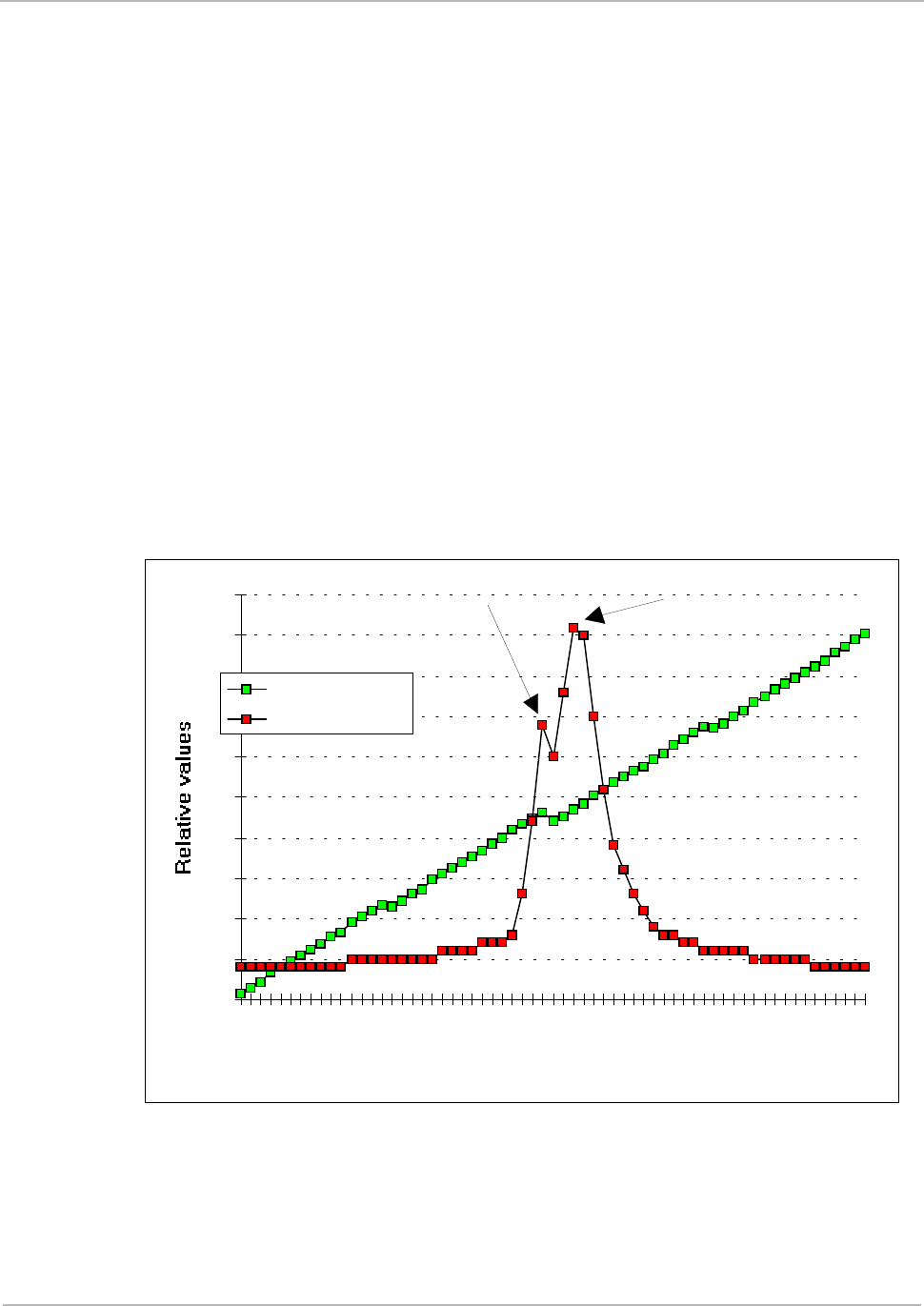
Counting-up of the binary weighted tuning capacitors is in principle done in the
following way:
1. No jumpers connected.
2. connect C_ATC1 (J3 pins 1 and 2).
3. disconnect C_ATC1 and connect C_ATC2.
4. Connect both C_ATC1 and C_ATC2 (and so on).
However, the tuning steps do not offer an absolutely continuously increasing
function, due to component tolerances. It is therefore possible that when the tuning
value is increased by one binary step the total tuning capacity actually decreases
(especially from tuning step 31 to 32), which can result in the generated field
strength not steadily increasing (as shown in Figure 7). This is not the case when
using the Antenna Tuning Indicator tool (ATI) since the indicated resonance
condition is always correct.
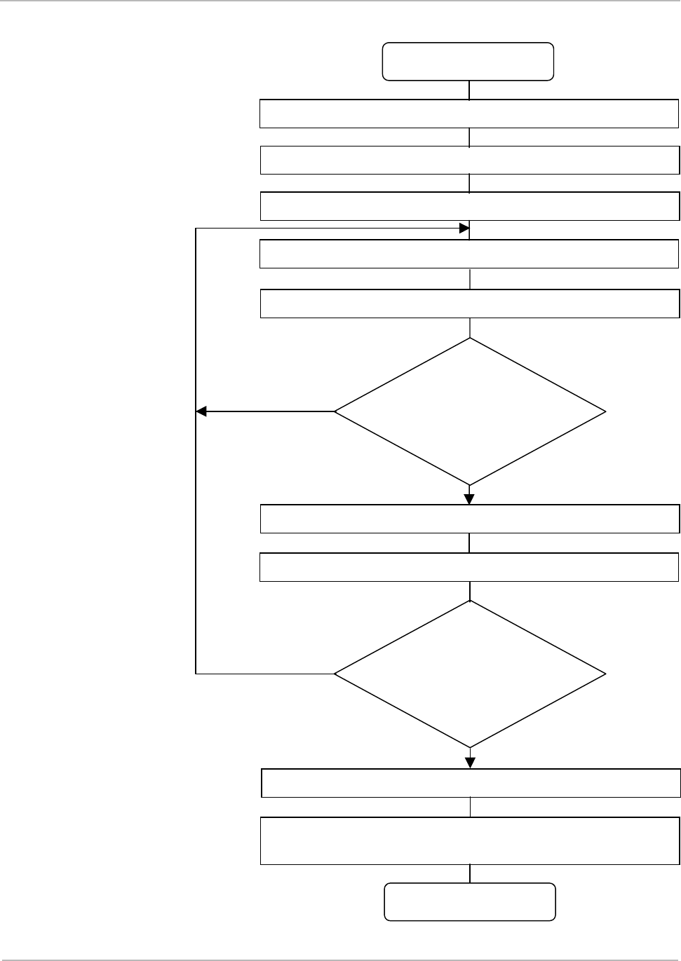
It is therefore recommended to perform resonance tuning according to the flow-
chart shown in Figure 8.
0
5
10
15
20
25
30
35
40
45
50
1 4 7 101316192225283134374043464952555861
Decimal value of tuning step
T uning capacity
Field strength
'false' resonance
point
correct resonance
point
Figure 7: Tuning Example showing Increase of Total Tuning Capacity
and Generated Field Strength (typical values)
High Performance RFM RI-RFM-007B April 1999
32
Figure 8: Flow-chart for Tuning the Antenna to Resonance
No
No
Yes
Yes
CONNECT ANTENNA TO THE RF MODULE
START
DISCONNECT ALL JUMPERS
CONTROL CURRENT INTO VSP PIN
INCREASE TUNING CAPACITY BY ONE BINARY STEP
CONTROL CURRENT INTO VSP PIN
MEASURED
VALUE HAS DECREASED IN
COMPARISON TO THE
PREVIOUS TUNING VALUE
INCREASE TUNING CAPACITY BY ONE BINARY STEP
CONTROL CURRENT INTO VSP PIN
MEASURED
VALUE HAS DECREASED IN
COMPARISON TO THE
PREVIOUS TUNING VALUE
DECREASE TUNING VALUE BY TWO BINARY STEPS
PLUG IN JUMPERS FOR TUNING THIS ANTENNA TO
THIS RF MODULE
STOP
33
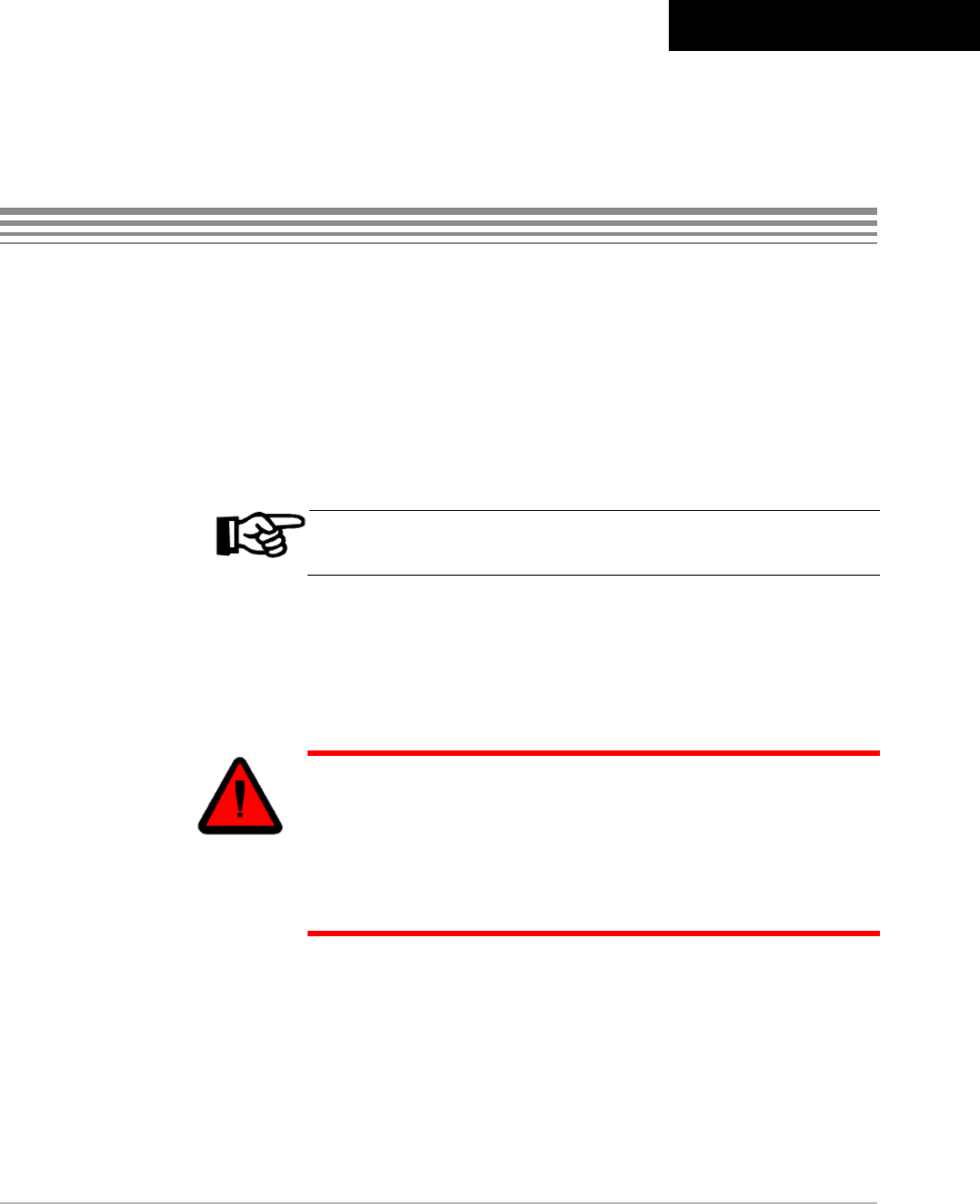
Expanding Antenna Tuning
Inductance Range
It is possible to expand the tuning range of the antenna inductance. This may be
necessary when TIRIS standard antennas are used close to metal, when antenna
extension cables are used or when customer specific antennas which might not be
within the necessary antenna tuning inductance range are used.
Note: Please remember that the capacitors of external modules have
to be able to withstand higher voltages when used together with a
RFM.
Expanding the antenna tuning inductance range to lower or higher values can be
done by connecting additional capacitors in parallel and in series to the antenna
resonator.
The capacitors have to be connected in parallel and in series in order to withstand
high voltages and currents occurring at the antenna resonance circuit.
WARNING: There is HIGH VOLTAGE present at all
antenna resonator components, which may be
harmful to health. The RFM must be switched OFF
while working on it. External components must be
mounted such that they cannot be accidentally
touched.
To ensure that the RFM functions correctly when the antenna tuning inductance
range is expanded, special capacitors, as listed below, must be used:
Capacitor type: - Polypropylene film capacitor
- Minimum 1250V DC operating voltage
- Capacitance tolerance: max. ±5%
- Type: SIEMENS "KP" or WIMA "FKP1"
Appendix 1
High Performance RFM RI-RFM-007B April 1999
34
The antenna tuning inductance range can be decreased to 13.7 µH in six ranges,
as shown in Figure 9 and Table 12.
Figure 9: Circuit for Expanding Antenna Tuning Range to Lower Values
Table 12: Capacitor Values for Expanding Antenna Tuning Range to Lower
Values
Antenna inductance range Capacitor value
24.1 µH to 25.9 µHC1, C2, C3, C4 = 3.3 nF
22.3 µH to 24.0 µHC1, C2, C3, C4 = 6.8 nF
20.4 µH to 22.2 µHC1, C2, C3, C4 = 11 nF
(10 nF and 1 nF in parallel)
18.4 µH to 20.3 µHC1, C2, C3, C4 = 16 nF
16.5 µH to 18.3 µHC1, C2, C3, C4 = 22 nF
13.7 µH to 16.4 µHC1, C2, C3, C4 = 32 nF
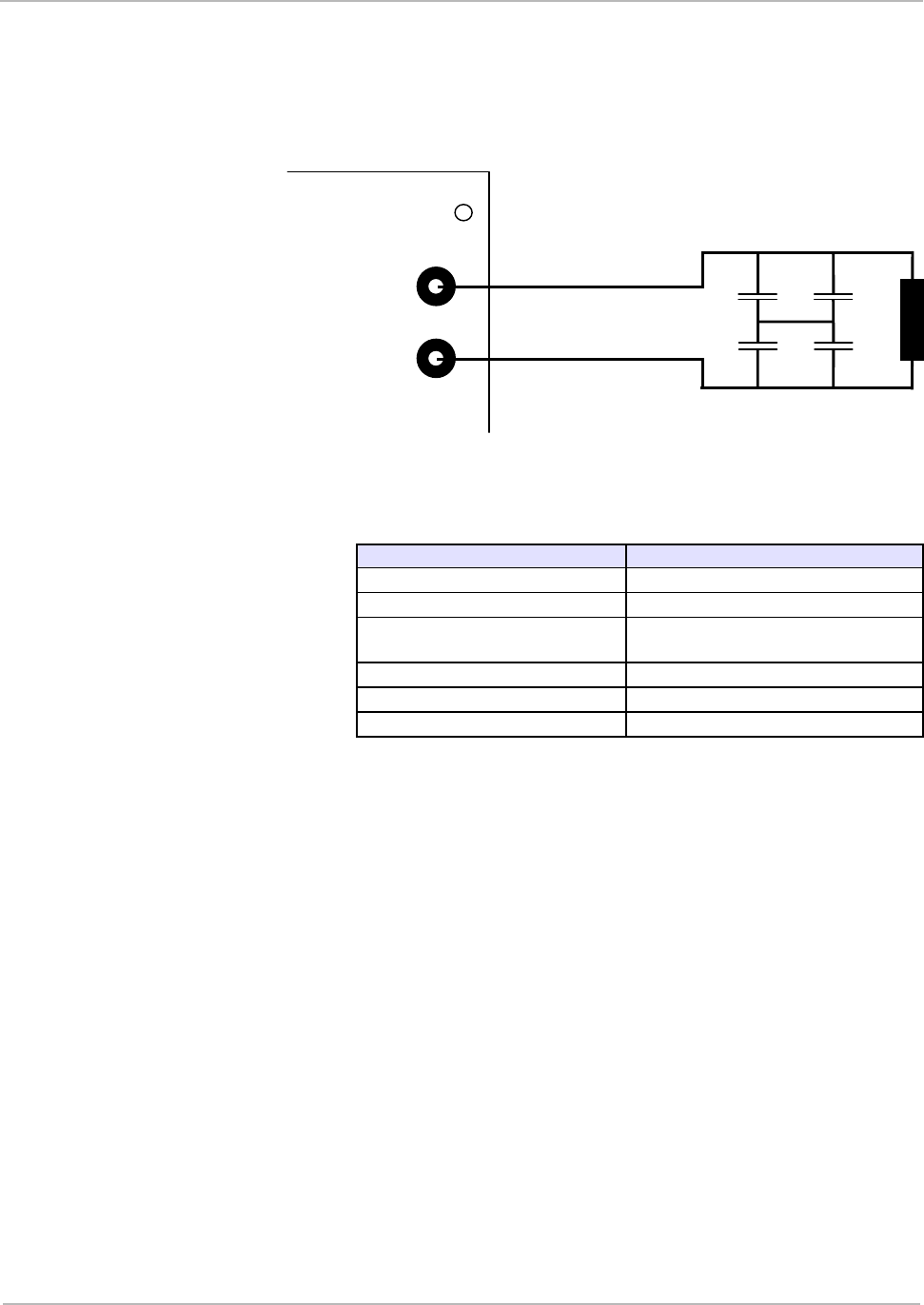
The antenna tuning inductance range can be increased to 37.6 µH in 7 ranges, as
shown in Figure 10 and Table 13.
As shown, three capacitors (C1, C2, C3) are connected in series with the antenna
coil. The specification for these capacitors is listed below:
Capacitor type: - Polypropylene film capacitor
- Minimum 1250 VDC operating voltage
- Capacitance: 47 nF ±2.5%
- Type: SIEMENS "KP" or WIMA "FKP1"
In addition to C1, C2 and C3, the capacitor C4 must be connected in parallel to the
RFM antenna terminals. Different capacitor values are used for each range, the
values being given in Table 13.
ANT 2
ANT 1
••
••
•
•
C1 C3
C4
C2
April 1999 Appendix 1
35
Figure 10: Circuit for Expanding Antenna Tuning Range to Higher Values
Table 13: Capacitor Values Expanding Antenna Tuning Range to Higher
Values
(C1, C2 & C3 = 47 nF)
Antenna inductance range Capacitor value
28.0 µH to 29.3 µHC4 = 18.3 nF
(parallel 6.8 nF, 6.8 nF, 4.7 nF)
29.4 µH to 31.0 µHC4 = 13.6 nF
(parallel 6.8 nF, 6.8 nF)
31.1 µH to 32.4 µHC4 = 10 nF
32.5 µH to 33.8 µHC4 = 6.8 nF
33.9 µH to 35.0 µHC4 = 3.98 nF
(parallel 3.3 nF, 0.68 nF)
35.1 µH to 36.2 µHC4 = 2.2 nF
36.3 µH to 37.6 µHC4 not needed
Two serial connected TIRIS standard antennas C4 = 3.3 nF
C2 and C3 not needed
Note: It is not recommended to use antennas with Q factors lower
than 50. Antennas with inductances lower than 13.7 µH or more than
37.8 µH should not be used except when connecting two antennas in
series since the additional capacitor values become very large.
Antennas with fewer turns (i.e. smaller inductance) generate less
charge-up field strength under the same operating conditions and in
addition also have less receive sensitivity. Using capacitors parallel to
the antenna resonator changes the coupling of the RFM's transmitter
power stage thus reducing the generated field strength.
In order to avoid adaptation problems, it is strongly recommended to
use standard TIRIS antennas.
ANT 2
ANT 1
••
•
•
•
•
•
•
•
C4 C1
C2
C3
•

37
Field Strength Adjustment
The magnetic field strength generated determines the charge-up distance of the
transponder. The higher the magnetic field strength, the further the transponder
charge-up distance. The charge-up distance does not, however, increase linearly
with the field strength.
The reading distance of a transponder is determined, amongst other factors, by the
charge-up distance and the local noise level. Increasing the charge-up field
strength does not necessarily increase the reading distance.
The field strength generated by the RFM depends on the four factors listed below:
1. Q factor of the antenna.
The Q factor is a measure of the efficiency of the antenna and therefore the higher
the Q factor of the antenna coil, the higher the field strength generated by the
RFM, assuming that all other parameters remain unchanged. The Q factor of the
antenna itself depends on the cross-sectional area of the wire, the wire type, the
size of the antenna and the type of antenna (gate or ferrite). The larger the cross-
sectional area of the RF braided wire, the higher the Q factor of the antenna. RF
braided wire gives a higher Q factor than solid wire assuming that all other
parameters remain unchanged.
2. Size of the antenna.
The larger the antenna, the higher the field strength which is generated by the
RFM, since the antenna covers a larger area and thus generates a higher flux
assuming that all other parameters remain unchanged. Large antennas have less
immunity to noise for receive functions than small antennas.
Appendix 2

High Performance RFM RI-RFM-007B April 1999
38
3. Supply voltage of the RFM power stage.
The higher the supply voltage of the RFM transmitter power stage (VSP voltage),
the higher the field strength which is generated by the RFM assuming that all other
parameters remain unchanged. However, the generated field strength does not
increase linearly with VSP supply voltage. In addition, ferrite core antennas show
saturation effects (saturation means here that the ferrite core cannot generate
more magnetic field strength, even with a higher input current).
4. The oscillator signal pulse width.
The bigger the selected transmitter oscillator signal pulse width, the higher the
magnetic field strength which is generated by the RFM, since more power is fed
into the antenna resonator by the transmitter power stage assuming that all other
parameters remain unchanged.
The generated field strength can be measured in several ways. It may be
measured using a calibrated field strength meter or by measuring the antenna
resonance voltage using an oscilloscope and then calculating the field strength.
In summary: the generated field strength of an antenna can be adjusted with the
supply voltage VSP of the RFM transmitter power stage and by selecting the
corresponding oscillator signal pulse width.
In cases where low field strengths should be generated with large antennas (RI-
ANT-G01 and RI-ANT-G03), the antenna resonator can be additionally damped by
closing jumper JP3.
Using this optional damping function allows the field strength to be again fine-tuned
to meet FCC/PTT regulations with selection of the oscillator signal pulse width in a
wide range of both larger and smaller values.
CAUTION: This damping option can only be used together
with the TIRIS standard antennas RI-ANT-G01 and RI-ANT-
G03. Only a certain maximum antenna resonance voltage is
allowed for this option. Please refer to Section 2.1,
Recommended Operating Conditions, for details.
Note: For correct adjustment of field strength according to FCC/PTT
values, especially for customized antennas, a calibrated field strength
meter must be used. Field strength measurements must be taken on a
free field test site according to VDE 0871 or equivalent regulation.

39
Adjustment of Oscillator Signal
Pulse Width
The RFM has an built-in feature to allow setting of the pulse width of the transmitter
signal coming from the oscillator. This enables the generated field strength to be
reduced from 50% down to 0%.
For this purpose a pulse width setting resistor may be inserted between J4 pins 3
and 4 on the RFM. Inserting a smaller resistance value decreases the pulse width
and thus also the field strength. As default, no resistor is connected, thus selecting
the maximum pulse width of 50% and the maximum field strength. By connecting a
shorting bridge, the smallest pulse width of approximately 0% is selected.
Table 14 provides an overview of oscillator signal pulse width and corresponding
field strength reduction when different oscillator signal pulse widths are selected by
connecting different resistor values.
Appendix 3
High Performance RFM RI-RFM-007B April 1999
40
Table 14: Oscillator Signal Pulse Width versus Resistor Value (estimated
values)
Resistor value
[kΩ
ΩΩ
Ω]Oscillator signal
pulse width [%] Field strength
reduction [dB]
open 50 0
151 37 -3
59 25 -6
17 12 -12
10 6 -18
shorted 0 ∞
CAUTION: When using pulse widths smaller than 50%, the
RFM transmitter power stage works less efficiently. This
leads to an increased power dissipation and thus to a
higher temperature of the transmitter power stage. Ensure
that the antenna resonance voltage does not exceed 200
Vp when the selected oscillator signal pulse width setting
is smaller than 25%.
Note: The pulse width for an oscillator signal pulse width setting of 5%
and smaller is extremely short. The pulse response of the RFM
transmitter power stage to this short pulse is different for each unit. In
order to have reproducible field strength values for different RFMs, it is
not recommended to use the smallest pulse width setting.

41
Threshold Level Adjustment
The RFM has a built-in receive signal field strength detector with the output signal
RXSS- and an on-board potentiometer (R409) to adjust the threshold level of field
strength detection. The digital output RXSS- is used for wireless synchronization of
two or more reading units. This is necessary to ensure that if more than one
reading unit is in an area, they do not interfere with each other. The Control Module
software monitors the RXSS- signal to detect whether other reading units are
transmitting. The Control Module can operate the transmitter of the RFM such that
the reading units either transmit simultaneously or alternately. In this way the read
cycles of each of the reading units occur at the same time or at secure different
times. Depending on the antenna type used and the local noise level, the RXSS-
threshold level has to be adjusted. This needs to be done after the antenna has
been tuned to resonance. It is recommended to use a small screwdriver to adjust
the RXSS- threshold level. The R409 potentiometer is located on the upper side of
the RFM board near connector switch SW1. Turning the potentiometer all the way
clockwise (right-hand stop), results in minimum threshold sensitivity, i.e. the RXSS-
signal will be activated at high receive field strength. This is the default position and
can be used for standard gate antennas. It may be necessary to increase the
sensitivity when using ferrite core antennas. If there is high noise level in the area,
it is necessary to adjust the RXSS- threshold level.
Adjust the RXSS- threshold level as follows:
1. Turn the RXSS- threshold level potentiometer fully counter-clockwise (left-hand
stop).
2. Deactivate the transmitter by jumpering pin 1 to pin 3 of connector J2.
3. Ensure that no other reading units are transmitting, by connecting pin 1 to pin 3
of connector J2 (jumper) of all other RFMs in the area.
4. Monitor the voltage at RXSS- output pin with a voltmeter or an oscilloscope.
Appendix 4

High Performance RFM RI-RFM-007B April 1999
42
5. Turn the RXSS- threshold level adjustment potentiometer on the RFM
clockwise, until the RXSS- output is just statically inactive. "Statically" means
no voltage spikes present on the RXSS- signal. 'Inactive' means that the
receive signal strength is below the RXSS- threshold level and not triggering
RXSS- (the RXSS- output voltage remains > 4 V).
6. Remove all jumpers connected to J2
Note: Reducing the RXSS- threshold level sensitivity (turning the
potentiometer clockwise), reduces the sensitivity of the built-in receive
signal strength detector. This has the effect that the distance for
wireless detection of other transmitting reading units is decreased,
leading to reduction of wireless synchronization distance. The wireless
synchronization distance between two reading units is normally about
15 meters for two aligned stick antennas (RI-ANT-S02) with maximum
receive field strength detection sensitivity.
When the RXSS- threshold level is adjusted such that it is too
sensitive, then the RXSS- output is constantly active (i.e. low RXSS-
output level). Therefore a Control Module assumes that another
reading unit is transmitting and continually tries to synchronise to this
other reading unit. As a result, the reading repetition rate decreases
from approximately 10 down to 5 readings per second. This reading
unit can additionally no longer synchronise to other reading units,
causing interference with other reading units and reading at all
reading units becomes impossible.
The RXSS- threshold level must be adjusted individually for every
RFM and reading system antenna. In addition, the RXSS- threshold
level must be individually adjusted to the local noise level in the
application area where the antenna is used.
As high noise levels mean that the RXSS- threshold level must be
adjusted to a less sensitive value, it is recommended to reduce the
local noise level in order to have high synchronization sensitivity and a
long reading distance.
The RXSS- threshold level must be adjusted so that no spikes occur
on the RXSS- signal output since these lead to an incorrect
synchronization function. An oscilloscope should therefore be used
when adjusting the threshold level.
The Antenna Tuning Indicator (RI-ACC-ATI2) accessory can be used
to adjust the RXSS- threshold level, since this device automatically
switches the transmitter off and has an internal spike extension circuit,
causing the RXSS- threshold level to be adjusted such that no spikes
occur on the RXSS- output.

43
Transmitter Carrier Phase
Synchronization (CPS)
In some applications it is necessary to use several charge-up antennas close to
each other. Under these circumstances, the magnetic charge-up fields generated
by different antennas superimpose on each other and may cause a beat effect on
the magnetic charge-up field, due to the slightly different transmit frequencies of
different RFMs.
The impact of this effect depends on three factors:
1. Antenna size:
The larger the size of the antennas, the further the distance between the
antennas must be, so that this effect does not occur.
2. Magnetic field strength:
The stronger the generated magnetic field strength, the further the distance
between the antennas must be such that the effect does not occur.
3. Orientation and distance between antennas:
Increasing the distance between antennas decreases the impact of this effect.
Note: Putting two antennas close together also changes antenna
inductance, so that the antennas may no longer be tuneable to
resonance.
Appendix 5
High Performance RFM RI-RFM-007B April 1999
44
If several antennas are used close to each other, a check should be made to
determine if the charge-up field strength changes regularly (i.e. beat effect ). This
may be checked by verifying the antenna resonance voltage with an oscilloscope.
If the antenna resonator voltage changes periodically by more than approximately
5% of the full amplitude it is appropriate to use wired transmitter carrier phase
synchronization.
In addition, the distances given in Table 15 can be used as a guideline to
determine when it is necessary to cross-check for beat effect. If these distances
are less than the value given in Table 15, a check for beat effect should be made.
The values given refer to the distances shown in Figure 11 and are valid for
maximum charge-up field strength.
Figure 11: Distance between Antennas (top view)
Table 15: Maximum Distances between Antennas
Antenna type Distance D1 [m] Distance D2 [m]
RI_ANT_S02 <=> RI_ANT_S02 0,8 1,0
RI_ANT_G01 <=> RI_ANT_G01 1.7 1.5
RI_ANT_G02 <=> RI_ANT_G02 1.3 1.0
RI_ANT_G04 <=> RI_ANT_G04 2.0 1.7
This effect will not occur if the transmitters of different RFMs are operated from the
same oscillator signal. This is the reason why the pulse width modulated oscillator
signal is accessible at the connector J1.
Configuration
Master or Slave setting of a RFM is determined by switch 1 position 1 (SW1/1). If
this is in the ON position, the RFM is a MASTER, if in the OFF position, it is a
SLAVE. When a RFM has been configured as a master, then J1 pin 12 of this unit
should be connected to J1 pin 16 of the slave units to allow the master oscillator
output (CPS_OUT) to drive the slave oscillator inputs (CPS_IN). The logic ground
(e.g. J1 pin 1) of both master and slave units should be connected together.
Caution: Use overvoltage protection components at the
CPS connector for CPS lines between 0.5m and 5m.
Distance D1
Antenna 1 Antenna 2
Distance D2
Antenna 1 Antenna 2

April 1999 Transmitter Carrier Phase Synchronization
45
Note: When using the transmitter Carrier Phase Synchronization
feature, it is absolutely necessary that the read cycles of each of the
different Control Modules are synchronized. When the transmitter of
the oscillator MASTER RFM is not activated by its Control Module, the
oscillator signal output of the oscillator MASTER RFM is disabled.
This means that all the oscillator SLAVE RFMs have no transmitter
oscillator input signal and thus none of the oscillator SLAVE RFMs are
able to transmit.
The read cycles of all RFMs connected to this CPS interface must be synchronized
and all read cycles must occur simultaneously. Refer to the Hardware and
Software Manuals for the TIRIS Control Modules for more information about the
necessary wiring and settings for synchronization of the RFM when using
transmitter Carrier Phase Synchronization (CPS). If an application requires more
than one RFM to be used, or a longer Carrier Phase Synchronization line than that
specified in chapter 2, Specifications, must be used, it is necessary to drive the
pulse width modulated oscillator signal via a differential interface such as an
RS422 interface.
47
Noise Considerations
Noise can have a negative effect on the receive performance of the RFM. There
are two different kinds of noise: radiated and conducted. Their characteristics are
shown in Table 16.
Table 16: Characteristics of Radiated and Conducted Noise
Radiated Noise Conducted Noise
Source Inductive parts for example:
deflection coils, motor coils. Power units, for example: motors, switched
mode power supplies. Can be seen as voltage
spikes or ripple voltage.
Path Via magnetic fields. Galvanically conducted via all cables (supply
and interface) connected to the RFM.
Effect Disturbs receive function by
magnetic interference with signal
from transponder at the antenna.
Leads to malfunction and reduced sensitivity of
receiver circuitry due to, for example, interfered
supply voltage.
Conducted noise can also cause radiated noise.
Method for detecting and distinguishing between noise types:
The principle of this procedure is to eliminate any conducted noise from the supply
and all interface lines. In order to do this test the RFM must be powered from a
battery (for example: 9 V, 20 mA) in order to eliminate any conducted noise from a
power supply. Conducted noise via the interface lines is eliminated for this test by
simply disconnecting all interface lines to the RFM. The measurement criteria for
low noise is the amplitude of the receive signal strength detector of the RFM.
The test pin RSTP at connector J1 pin 10 carries an analog output voltage
indicating the receive signal strength. This voltage should be measured in
combination with the antenna RI-ANT-G02. The necessary set-up for this test is
shown in Figure 12. This configuration operates the RFM from a battery and has no
interface line connected. As the transmitter is switched off in this configuration, a
normal battery may be used. A low noise level is indicated by an RSTP voltage of
less than 1.0 VDC when using antenna RI-ANT-G02.
Appendix 6
High Performance RFM RI-RFM-007B April 1999
48
Note: Both noise types can be either differential or common mode
noise. Use common mode noise filters (for example: a BALUN
transformer) to reduce common mode noise and use selective filters
to reduce differential noise.
The following procedure for testing for noise impact should be implemented when
the normal set-up for the RFM and antenna gives bad reading distances, even
though the antenna is correctly tuned for sufficient transponder charge-up.
Try the configuration shown in Figure 12. If this configuration shows bad noise
conditions (RSTP voltage more than approximately 1.0 VDC) then the problem is
radiated noise.
Eliminate noise sources or try special antennas (e.g. noise-balanced antennas).
1. When the configuration of Figure 12 shows good noise conditions (RSTP
voltage less than 1.0 VDC) then the problem is conducted noise.
2. Change the configuration so that the interface lines are again connected to the
RFM with the transmitter still switched off. If the RSTP voltage now indicates
bad noise conditions, the conducted noise is coming via the interface lines.
3. Try to eliminate the noise on the interface lines. See Appendix 7, Over Voltage
Protection.
4. When the configuration above (interface lines connected) shows good noise
conditions (RSTP voltage less than 1.0 VDC), then the problem is conducted
noise via the supply lines.
5. Try to eliminate the noise on the supply lines. See Appendix 7, Over Voltage
Protection.
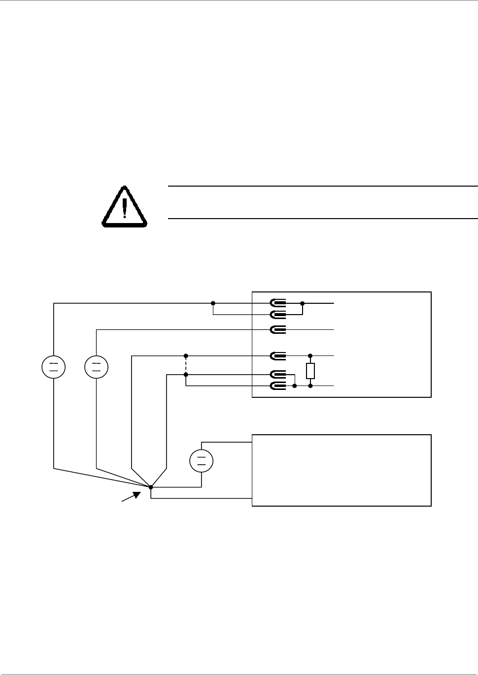
Figure 12: Noise Testing Configuration
GND 1
TIRIS standard
antenna
RI-ANT-G02
J1
RSTP
VSP 13
VSP 11
GNDP 9
7
VSL 3
10
ANT 1
ANT 2
•
•
•
•

49
Over Voltage Protection
For applications where there is a risk that voltage spikes and noise are on the lines
to the RFM, additional protection circuitry and filters must be added.
A proposal on how this may be achieved is shown in Figure 13, and this circuit may
be used as a guideline for protection circuitry. This may not be sufficient for all
applications, however, and must be checked individually when necessary.
1. The supply input has to be protected against voltage spikes. R1 and D1 fulfil
this purpose. Zener diode D1 clamps the voltage spikes to 18 volts so that the
maximum allowed transmitter power stage supply voltage is not appreciably
exceeded. For diode D1, type ZY18 is recommended, this type having a 2 W
power dissipation. If a higher current is needed, dump type ZX18 may be used,
this diode having a 12.5 W power dissipation.
2. The Common Mode Choke Coil and the capacitors C1 and C2 are used to
reduce the conducted noise coming to the RFM via the supply lines.
3. All input and output signals should be protected with 5.6 V zener diodes. The
specified type can dump 1.3 W.
4. The coils L1 to L6 are ferrite beads and should put in series to the line when
conducted noise is observed entering via the interface lines.
5. The varistor V1 protects the antenna circuit against high voltage induced at the
antenna coil, for example by lightning. The type of varistor given is commonly
available but may not be sufficient for protection in all cases.
Note: The zener diodes types given in Figure 13 are commonly used
types, not special suppresser diodes for fast voltage spike
suppression. If the application requires it, special suppresser diodes
should be used.
Appendix 7
High Performance RFM RI-RFM-007B April 1999
50
Figure 13: Circuit for Overvoltage Protection
All components must be mounted close to the RFM with the shortest possible
wiring
C1: 100 nF Ceramic R1: 1 Ohm / 2W V1: Varistor 420V
e.g Siemens S10V-
520K420
C2: 100 µF low ESR R2, R3, R4, R5, R6, R7:
22 Ohm / 0.25W
CHOKE: Common
Mode Choke Coil
L1, L2, L3, L4, L5, L6:
Ferrite beads
D1: ZY18 resp. ZX18
D2,D3, D4, D5, D6, D7:
BZX85C5V6