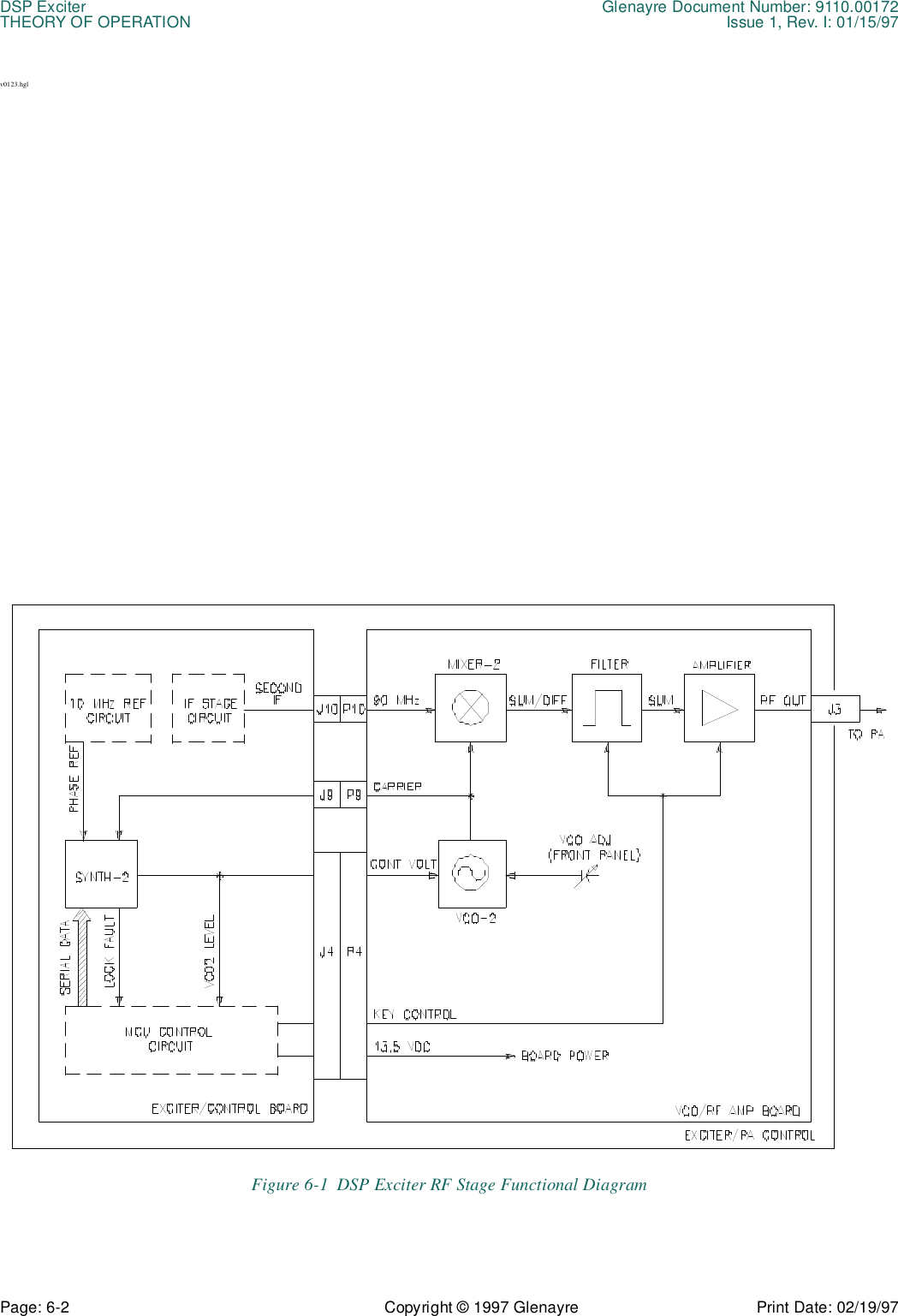
Glenayre Electronics GL-T8600-CN Base Station User Manual Users manual part 5

Glenayre Electronics Inc Base Station Users manual part 5

Users manual part 5

Print Date: 02/18/97 Copyright © 1997 GlenayreDSP Exciter Issue 1, Rev. I: 01/15/97Specifications subject to change without noticeCopyright © 1997 GlenayreAll rights reserved. No part of this work may be reproduced or copied in any form or by any means—graphic, electronic, or mechanical, including photocopying, recording, taping, or information-retrieval system—without written permission of Glenayre.DSP Exciter With Wideband OptionUSER MANUALPN 9110.00172 (old part number = 916-T70A-003)REV IRELEASED
DSP Exciter Glenayre Document Number: 9110.00172Document Change Record Issue 1, Rev. I: 01/15/97Copyright © 1997 Glenayre Print Date: 02/18/97Document Change RecordIssue: 1Date: 05/09/95Changes: none, originalIssue: Rev BDate: 02/07/96Changes: added wideband informationIssue: Rev CDate: 02/29/96Changes: changed jumpers, drawing main bdIssue: Rev DDate: 4/25/96Changes: changed VCO-2 status readingIssue: Rev EDate: 5/14/96Changes: added Over-The-Link and On-The-Fly informationIssue: Rev FDate: 5/23/96Changes: added one RU space for reinstallation and net channel change time for setupIssue: Rev GDate: 9/03/96Changes: changed PA fault input pin 11 on Table 4-4Issue: Rev HDate: 9/20/96Changes: revised chapter 4 jumper information, added Table 4-5Issue: Rev IDate: 01/15/97Changes: added and changed VCO board numbers in Table 3-1
Glenayre Document Number: 9110.00172 DSP ExciterIssue 1, Rev. I: 01/15/97 Table of ContentsPrint Date: 02/19/97 Copyright © 1997 Glenayre Page: -i    sec_1.tocTable of Contents1  GENERAL   .  .  .  .  .  .  .  .  .  .  .  .  .  .  .  .  .  .  .  .  .  .  .  .  .  .  .  .  .  .  .  .  .  .  .  .  1-11.1  Manual Scope  .   .   .   .   .   .   .   .   .   .   .   .   .   .   .   .   .   .   .   .   .   .   .   .  1-11.1.1  Applicable Documents  .  .  .  .  .  .  .  .  .  .  .  .  .  .  .  .  .  .  .  .  .  .   1-11.2  Manual Sections  .   .   .   .   .   .   .   .   .   .   .   .   .   .   .   .   .   .   .   .   .   .   .  1-11.3  Exciter Identification   .   .   .   .   .   .   .   .   .   .   .   .   .   .   .   .   .   .   .   .   .  1-12  SPECIFICATIONS .  .  .  .  .  .  .  .  .  .  .  .  .  .  .  .  .  .  .  .  .  .  .  .  .  .  .  .  .  .  .  .  2-13  DESCRIPTION .  .  .  .  .  .  .  .  .  .  .  .  .  .  .  .  .  .  .  .  .  .  .  .  .  .  .  .  .  .  .  .  .  .  3-13.1  Introduction .   .   .   .   .   .   .   .   .   .   .   .   .   .   .   .   .   .   .   .   .   .   .   .   .  3-13.2  Physical Description    .   .   .   .   .   .   .   .   .   .   .   .   .   .   .   .   .   .   .   .   .  3-13.3  Simplified Block-Diagram Description   .   .   .   .   .   .   .   .   .   .   .   .   .   .  3-34  INSTALLATION AND SETUP  .  .  .  .  .  .  .  .  .  .  .  .  .  .  .  .  .  .  .  .  .  .  .  .  .  4-14.1  Precautions and Hazards  .   .   .   .   .   .   .   .   .   .   .   .   .   .   .   .   .   .   .   .  4-14.2  Test Equipment and Tools Required   .   .   .   .   .   .   .   .   .   .   .   .   .   .   .  4-14.3  Component and Adjustment Locations   .   .   .   .   .   .   .   .   .   .   .   .   .   .  4-14.4  Installation   .   .   .   .   .   .   .   .   .   .   .   .   .   .   .   .   .   .   .   .   .   .   .   .   .  4-14.4.1  Inspection .  .  .  .  .  .  .  .  .  .  .  .  .  .  .  .  .  .  .  .  .  .  .  .  .  .  .  .  .   4-14.4.2  Power Requirement .  .  .  .  .  .  .  .  .  .  .  .  .  .  .  .  .  .  .  .  .  .  .  .   4-24.4.3  Input/Output Connections   .  .  .  .  .  .  .  .  .  .  .  .  .  .  .  .  .  .  .  .   4-24.4.4  Signal Functions   .  .  .  .  .  .  .  .  .  .  .  .  .  .  .  .  .  .  .  .  .  .  .  .  .   4-24.4.5  Switches and Jumpers   .  .  .  .  .  .  .  .  .  .  .  .  .  .  .  .  .  .  .  .  .  .   4-34.5  Setup    .   .   .   .   .   .   .   .   .   .   .   .   .   .   .   .   .   .   .   .   .   .   .   .   .   .   .  4-44.6  Ultimate Disposition    .   .   .   .   .   .   .   .   .   .   .   .   .   .   .   .   .   .   .   .   .  4-45  OPERATION  .  .  .  .  .  .  .  .  .  .  .  .  .  .  .  .  .  .  .  .  .  .  .  .  .  .  .  .  .  .  .  .  .  .  .  5-15.1  Front-Panel Controls and Indicators    .   .   .   .   .   .   .   .   .   .   .   .   .   .   .  5-15.2  Operating Instructions .   .   .   .   .   .   .   .   .   .   .   .   .   .   .   .   .   .   .   .   .  5-16  THEORY OF OPERATION .  .  .  .  .  .  .  .  .  .  .  .  .  .  .  .  .  .  .  .  .  .  .  .  .  .  .  6-16.1  Exciter/PA Control  .   .   .   .   .   .   .   .   .   .   .   .   .   .   .   .   .   .   .   .   .   .  6-16.1.1  Reference Source .  .  .  .  .  .  .  .  .  .  .  .  .  .  .  .  .  .  .  .  .  .  .  .  .   6-16.1.2  Main Circuit Frequencies .  .  .  .  .  .  .  .  .  .  .  .  .  .  .  .  .  .  .  .  .   6-16.1.3  Controller Interface Connector Functions   .  .  .  .  .  .  .  .  .  .  .  .   6-16.2  Interface to Controller .   .   .   .   .   .   .   .   .   .   .   .   .   .   .   .   .   .   .   .   .  6-36.2.1  General  .  .  .  .  .  .  .  .  .  .  .  .  .  .  .  .  .  .  .  .  .  .  .  .  .  .  .  .  .  .   6-36.2.2  Interface Conversion Functions   .  .  .  .  .  .  .  .  .  .  .  .  .  .  .  .  .   6-3
DSP Exciter Glenayre Document Number: 9110.00172Table of Contents Issue 1, Rev. I: 01/15/97Page: -ii Copyright © 1997 Glenayre Print Date: 02/19/976.3  DSP Modulator  .   .   .   .   .   .   .   .   .   .   .   .   .   .   .   .   .   .   .   .   .   .   .    6-46.3.1  General  .  .  .  .  .  .  .  .  .  .  .  .  .  .  .  .  .  .  .  .  .  .  .  .  .  .  .  .  .  .    6-46.3.2  DSP Modulator Signal Flow .  .  .  .  .  .  .  .  .  .  .  .  .  .  .  .  .  .  .    6-46.4  IF Stage  .   .   .   .   .   .   .   .   .   .   .   .   .   .   .   .   .   .   .   .   .   .   .   .   .   .    6-76.4.1  Mixer-1 .  .  .  .  .  .  .  .  .  .  .  .  .  .  .  .  .  .  .  .  .  .  .  .  .  .  .  .  .  .    6-76.4.2  Filter   .  .  .  .  .  .  .  .  .  .  .  .  .  .  .  .  .  .  .  .  .  .  .  .  .  .  .  .  .  .  .    6-76.4.3  VCO-1  .  .  .  .  .  .  .  .  .  .  .  .  .  .  .  .  .  .  .  .  .  .  .  .  .  .  .  .  .  .    6-76.4.4  Synthesizer-1 .  .  .  .  .  .  .  .  .  .  .  .  .  .  .  .  .  .  .  .  .  .  .  .  .  .  .    6-76.5  MCU   .   .   .   .   .   .   .   .   .   .   .   .   .   .   .   .   .   .   .   .   .   .   .   .   .   .   .    6-86.5.1  Microcontroller Unit (MCU) .  .  .  .  .  .  .  .  .  .  .  .  .  .  .  .  .  .  .    6-86.5.2  Digital-to-Analog (D/A) Converter   .  .  .  .  .  .  .  .  .  .  .  .  .  .  .    6-96.5.3  8/16-Bit Converter  .  .  .  .  .  .  .  .  .  .  .  .  .  .  .  .  .  .  .  .  .  .  .  .    6-96.5.4  Read-Only Memory   .  .  .  .  .  .  .  .  .  .  .  .  .  .  .  .  .  .  .  .  .  .  .    6-96.5.5  VSWR-Fault Detector  .  .  .  .  .  .  .  .  .  .  .  .  .  .  .  .  .  .  .  .  .     6-146.5.6 Alarm Data-to-Logic Conversion   .  .  .  .  .  .  .  .  .  .  .  .  .  .  .     6-146.6  RF Assemblies   .   .   .   .   .   .   .   .   .   .   .   .   .   .   .   .   .   .   .   .   .   .      6-146.6.1   RF Stage Location .  .  .  .  .  .  .  .  .  .  .  .  .  .  .  .  .  .  .  .  .  .  .     6-146.6.2  RF Assemblies  .  .  .  .  .  .  .  .  .  .  .  .  .  .  .  .  .  .  .  .  .  .  .  .  .     6-146.7  Voltage Regulator Circuit  .   .   .   .   .   .   .   .   .   .   .   .   .   .   .   .   .   .      6-167  MAINTENANCE    .  .  .  .  .  .  .  .  .  .  .  .  .  .  .  .  .  .  .  .  .  .  .  .  .  .  .  .  .  .  .  .   7-17.1  Location of Maintenance Procedures     .   .   .   .   .   .   .   .   .   .   .   .   .   .    7-17.2  Test Equipment Required   .   .   .   .   .   .   .   .   .   .   .   .   .   .   .   .   .   .   .    7-17.3  VCO-2 Adjustment Procedure   .   .   .   .   .   .   .   .   .   .   .   .   .   .   .   .   .    7-17.3.1  VCO-2 Multichannel Adjustment Procedure   .  .  .  .  .  .  .  .  .  .    7-17.3.2  VCO-2 Single-Channel Adjustment Procedure   .  .  .  .  .  .  .  .  .    7-17.4  Over-The-Link Downloading    .   .   .   .   .   .   .   .   .   .   .   .   .   .   .   .   .    7-27.5  On-The-Fly Channel/Mode Changing   .   .   .   .   .   .   .   .   .   .   .   .   .   .    7-27.5.1  Programming Example .  .  .  .  .  .  .  .  .  .  .  .  .  .  .  .  .  .  .  .  .  .    7-37.6  16-Channel Operation    .   .   .   .   .   .   .   .   .   .   .   .   .   .   .   .   .   .   .   .    7-47.7  On-The-Fly Interface .   .   .   .   .   .   .   .   .   .   .   .   .   .   .   .   .   .   .   .   .    7-58  CHECKOUT AND TROUBLESHOOTING .  .  .  .  .  .  .  .  .  .  .  .  .  .  .  .  .  .   8-18.1  CHECKOUT  .   .   .   .   .   .   .   .   .   .   .   .   .   .   .   .   .   .   .   .   .   .   .   .    8-18.2  TROUBLESHOOTING     .   .   .   .   .   .   .   .   .   .   .   .   .   .   .   .   .   .   .    8-1
Glenayre Document Number: 9110.00172 DSP ExciterIssue 1, Rev. I: 01/15/97 Table of ContentsPrint Date: 02/19/97 Copyright © 1997 Glenayre Page: -iii    sec_1.toc9  REMOVAL AND REINSTALLATION   .  .  .  .  .  .  .  .  .  .  .  .  .  .  .  .  .  .  .  .  9-19.1  Exciter/PA Control Chassis .   .   .   .   .   .   .   .   .   .   .   .   .   .   .   .   .   .   .  9-19.1.1  Removal Procedure .  .  .  .  .  .  .  .  .  .  .  .  .  .  .  .  .  .  .  .  .  .  .  .   9-19.1.2  Reinstallation Procedure  .  .  .  .  .  .  .  .  .  .  .  .  .  .  .  .  .  .  .  .  .   9-19.2  Exciter Cover   .   .   .   .   .   .   .   .   .   .   .   .   .   .   .   .   .   .   .   .   .   .   .   .  9-29.2.1  Removal Procedure .  .  .  .  .  .  .  .  .  .  .  .  .  .  .  .  .  .  .  .  .  .  .  .   9-29.2.2  Reinstallation Procedure  .  .  .  .  .  .  .  .  .  .  .  .  .  .  .  .  .  .  .  .  .   9-29.3  Exciter/Control Board  .   .   .   .   .   .   .   .   .   .   .   .   .   .   .   .   .   .   .   .   .  9-59.3.1  Removal Procedure .  .  .  .  .  .  .  .  .  .  .  .  .  .  .  .  .  .  .  .  .  .  .  .   9-59.3.2  Reinstallation Procedure  .  .  .  .  .  .  .  .  .  .  .  .  .  .  .  .  .  .  .  .  .   9-59.4  Interface Board    .   .   .   .   .   .   .   .   .   .   .   .   .   .   .   .   .   .   .   .   .   .   .  9-89.4.1  Removal Procedure .  .  .  .  .  .  .  .  .  .  .  .  .  .  .  .  .  .  .  .  .  .  .  .   9-89.4.2  Reinstallation Procedure  .  .  .  .  .  .  .  .  .  .  .  .  .  .  .  .  .  .  .  .  .   9-89.5  VCO/RF Amplifier Board   .   .   .   .   .   .   .   .   .   .   .   .   .   .   .   .   .   .   .  9-89.5.1  Removal Procedure .  .  .  .  .  .  .  .  .  .  .  .  .  .  .  .  .  .  .  .  .  .  .  .   9-99.5.2  Reinstallation Procedure  .  .  .  .  .  .  .  .  .  .  .  .  .  .  .  .  .  .  .  .  .   9-910  OPTIONS  .  .  .  .  .  .  .  .  .  .  .  .  .  .  .  .  .  .  .  .  .  .  .  .  .  .  .  .  .  .  .  .  .  .  .  .   10-110.1  Exciter/PA Control with QT-1000 Interface   .   .   .   .   .   .   .   .   .   .   .    10-110.1.1  Reference Source  .  .  .  .  .  .  .  .  .  .  .  .  .  .  .  .  .  .  .  .  .  .  .  .    10-110.1.2  Controller Interface Connector Functions   .  .  .  .  .  .  .  .  .  .  .    10-110.1.3  QT-1000 Interface Conversion Functions   .  .  .  .  .  .  .  .  .  .  .    10-110.2  Exciter/PA Control with Standard Interface    .   .   .   .   .   .   .   .   .   .   .    10-510.2.1  Reference Source  .  .  .  .  .  .  .  .  .  .  .  .  .  .  .  .  .  .  .  .  .  .  .  .    10-510.2.2  Controller Interface Connector Functions   .  .  .  .  .  .  .  .  .  .  .    10-510.2.3  Standard Interface Conversion Functions   .  .  .  .  .  .  .  .  .  .  .    10-510.3  Exciter/PA Control with I20 Interface    .   .   .   .   .   .   .   .   .   .   .   .   .    10-810.3.1  Reference Source  .  .  .  .  .  .  .  .  .  .  .  .  .  .  .  .  .  .  .  .  .  .  .  .    10-810.3.2  Controller Interface Connector Functions   .  .  .  .  .  .  .  .  .  .  .    10-810.3.3  I20 Interface Conversion Functions   .  .  .  .  .  .  .  .  .  .  .  .  .  .    10-9
DSP Exciter Glenayre Document Number: 9110.00172Table of Contents Issue 1, Rev. I: 01/15/97Page: -iv Copyright © 1997 Glenayre Print Date: 02/19/97
Glenayre Document Number: 9110.00172 DSP ExciterIssue 1, Rev. I: 01/15/97 List of FiguresPrint Date: 02/19/97 Copyright © 1997 Glenayre Page: -v    sec_1.lofList of FiguresFigure 1-1  DSP Exciter Isometric View  .  .  .  .  .  .  .  .  .  .  .  .  .  .  .  .  .  .  .  .  .  .  .  1-2Figure 3-1  DSP Exciter Rear View    .  .  .  .  .  .  .  .  .  .  .  .  .  .  .  .  .  .  .  .  .  .  .  .  .  3-4Figure 3-2  DSP Exciter Top Viewwith Internal Controls and Indicators   .  .  .  .  .  .  .  .  .  .  .  .  .  .  .  .  .  .  3-5Figure 3-3  DSP Exciter Simplified Functional Diagram    .  .  .  .  .  .  .  .  .  .  .  .  .  .  3-6Figure 4-1  DSP Exciter/PA Control Circuit Boards Interconnection Diagram .  .  .  .  .  .  .  .  .  .  .  .  .  .  .  .  .  .  .  .  .  .  .  .  .  4-5Figure 5-1  Front-Panel Controls and Indicators  .  .  .  .  .  .  .  .  .  .  .  .  .  .  .  .  .  .  .  5-2Figure 6-1  DSP Exciter RF Stage Functional Diagram   .  .  .  .  .  .  .  .  .  .  .  .  .  .  .  6-2Figure 6-2  DSP Exciter MCU Circuit Functional Diagram  .  .  .  .  .  .  .  .  .  .  .  .  .  6-6Figure 6-3  DSP Exciter-to-Controller Functional Diagram  .  .  .  .  .  .  .  .  .  .  .  .   6-10Figure 6-4  DSP Exciter Detailed Functional Diagram .  .  .  .  .  .  .  .  .  .  .  .  .  .  .   6-12Figure 6-5  DSP Exciter IF-Stage DetailedFunctional Diagram   .  .  .  .  .  .  .  .  .  .  .  .  .  .  .  .  .  .  .  .  .  .  .  .  .  .   6-13Figure 7-1  On-The-Fly C2000 Control Lines to DSP Exciter  .  .  .  .  .  .  .  .  .  .  .  .  7-5Figure 9-1  DSP Exciter Chassis Removal and Reinstallation    .  .  .  .  .  .  .  .  .  .  .  .  .  .  .  .  .  .  .  .  .  .  .  .  .  .  .  .  9-3Figure 9-2  DSP Exciter Cover Removal and Reinstallation    .  .  .  .  .  .  .  .  .  .  .  .  .  .  .  .  .  .  .  .  .  .  .  .  .  .  .  .  9-4Figure 9-3  DSP Exciter Control Board Removal and Reinstallation   .  .  .  .  .  .  .  .  9-7Figure 9-4  DSP Exciter External Interface I/O BoardRemoval and Reinstallation   .  .  .  .  .  .  .  .  .  .  .  .  .  .  .  .  .  .  .  .  .  .   9-10Figure 9-5  DSP Exciter Interface Board Removal and Reinstallation .  .  .  .  .  .  .   9-11
DSP Exciter Glenayre Document Number: 9110.00172List of Figures Issue 1, Rev. I: 01/15/97Page: -vi Copyright © 1997 Glenayre Print Date: 02/19/97
Glenayre Document Number: 9110.00172 DSP ExciterIssue 1, Rev. I: 01/15/97 List of TablesPrint Date: 02/19/97 Copyright © 1997 Glenayre Page: -vii    sec_1.lotList of TablesTable 1-1 Manual Contents  .  .  .  .  .  .  .  .  .  .  .  .  .  .  .  .  .  .  .  .  .  .  .  .  .  .  .  .  .  1-1Table 2-1 Exciter Specifications.  .  .  .  .  .  .  .  .  .  .  .  .  .  .  .  .  .  .  .  .  .  .  .  .  .  .  2-1Table 3-1 Part Numbers of VCO/RF Amplifier Boards .  .  .  .  .  .  .  .  .  .  .  .  .  .  .  3-1Table 3-2 Part Numbers of Interface Boards   .  .  .  .  .  .  .  .  .  .  .  .  .  .  .  .  .  .  .  .  3-2Table 3-3 Part Numbers of Interface I/O Boards  .  .  .  .  .  .  .  .  .  .  .  .  .  .  .  .  .  .  3-2Table 3-4 Assembly and Control Board Numbers.  .  .  .  .  .  .  .  .  .  .  .  .  .  .  .  .  .  3-3Table 4-1 Test Equipment Required.  .  .  .  .  .  .  .  .  .  .  .  .  .  .  .  .  .  .  .  .  .  .  .  .  4-1Table 4-2 DSP Exciter I/O Connectors  .  .  .  .  .  .  .  .  .  .  .  .  .  .  .  .  .  .  .  .  .  .  .  4-2Table 4-3 VT100 Interface Connector J3 Pin Assignments .  .  .  .  .  .  .  .  .  .  .  .  .  4-3Table 4-4 Control Board Connector J6 Pin Assignments .  .  .  .  .  .  .  .  .  .  .  .  .  .  4-3Table 4-5 Exciter Control Board Jumper Positions  .  .  .  .  .  .  .  .  .  .  .  .  .  .  .  .  .  4-4Table 6-1 Exciter RF/Main Circuit Frequencies.  .  .  .  .  .  .  .  .  .  .  .  .  .  .  .  .  .  .  6-1Table 7-1 Deviation and Offset Programming.  .  .  .  .  .  .  .  .  .  .  .  .  .  .  .  .  .  .  .  7-3Table 10-1 Interface Board Connector J4 (QT-1000).  .  .  .  .  .  .  .  .  .  .  .  .  .  .  .  .10-3Table 10-2 Receiver Connector J5 Pin Functions (QT-1000 with external I/O board) .  .  .  .  .  .  .  .  .  .  .  .  .  .  .  .  .  .  .  .10-4Table 10-3 Remote Select Input vs. Channel (QT-1000) .  .  .  .  .  .  .  .  .  .  .  .  .  .  .10-4Table 10-4 Remote Select Input vs. Mode (QT-1000)  .  .  .  .  .  .  .  .  .  .  .  .  .  .  .  .10-4Table 10-5 Interface Board Connector J4 (Standard) .  .  .  .  .  .  .  .  .  .  .  .  .  .  .  .  .10-7Table 10-6 Remote Select Input vs. Channel (standard)  .  .  .  .  .  .  .  .  .  .  .  .  .  .  .10-7Table 10-7 Remote Select Input vs. Mode (standard)   .  .  .  .  .  .  .  .  .  .  .  .  .  .  .  .10-8Table 10-8 Interface Board Connector J1.  .  .  .  .  .  .  .  .  .  .  .  .  .  .  .  .  .  .  .  .  . 10-10Table 10-9 Interface Board Connector J2.  .  .  .  .  .  .  .  .  .  .  .  .  .  .  .  .  .  .  .  .  . 10-11Table 10-10 Remote Select Input vs. Channel (I20) .  .  .  .  .  .  .  .  .  .  .  .  .  .  .  .  . 10-11Table 10-11 Remote Select Input vs. Mode (I20)  .  .  .  .  .  .  .  .  .  .  .  .  .  .  .  .  .  . 10-11
DSP Exciter Glenayre Document Number: 9110.00172List of Tables Issue 1, Rev. I: 01/15/97Page: -viii Copyright © 1997 Glenayre Print Date: 02/19/97
Glenayre Document Number: 9110.00172 DSP ExciterIssue 1, Rev. I: 01/15/97 GENERALPrint Date: 02/19/97 Copyright © 1997 Glenayre Page: 1-1    sec_11 GENERAL1.1 Manual ScopeThis manual is intended for use as a technical reference guide to the Glenayre DSP exciterand contains information on exciter connection, setup, and maintenance.1.1.1 Applicable DocumentsApplicable Glenayre documents are listed in the applicable system manual.1.2 Manual SectionsRefer to Table 1-1, Manual Contents. Also refer to table of contents in this manual.1.3 Exciter IdentificationRefer to Figure Figure 1-1, DSP Exciter Isometric View, for an overall view of theexciter.Table 1-1  Manual Contents section No. and title contents1 General this section2 Specifications exciter specifications 3 Descriptions listing of options and assemblies covered, simplified description, physical description, simplified block theory of operation4 Installation and Setup exciter installation, setup, and lists of connections5 Operation list, description, and location of operator controls and indicators6 Theory of Operation assembly-level description of exciter operation7 Maintenance exciter maintenance8 Checkout and Troubleshooting exciter checkout and troubleshooting9 Removal and Reinstallation procedures for removing and reinstalling exciter and exciter assemblies10 Options  list and discussion of user selectable options
DSP Exciter Glenayre Document Number: 9110.00172GENERAL Issue 1, Rev. I: 01/15/97Page: 1-2 Copyright © 1997 Glenayre Print Date: 02/19/97v0250.hgl Figure 1-1  DSP Exciter Isometric View
Glenayre Document Number: 9110.00172 DSP ExciterIssue 1, Rev. I: 01/15/97 SPECIFICATIONSPrint Date: 02/19/97 Copyright © 1997 Glenayre Page: 2-1    sec_22 SPECIFICATIONSRefer to Table 2-1, Exciter Specifications, which lists the DSP exciter specifications.Where possible, EIA or I-EIS A measuring methods were used in determining specifica-tions. Note that some specifications are not addressed by either set of standards or theprescribed methods were impractical. Table 2-1  Exciter Specifications characteristic condition specificationadjacent-channel noise 25-kHz channel spacing, in analog mode -85 dBc25-kHz channel spacing, in FSK mode -75 dBcalternate channel noise 25-kHz channel spacing -95 dBcspurious -90 dBcoperating frequency range determined by installed VCO/RF board refer to Table 3-1RF output power keyed 250 mW nominalcarrier frequency stability steady state, -30° to +60° C10-MHz reference, int=0.005 ppm/yr, ext=0.1 ppm/yrFSK frequency/modulation stability relative to carrier frequency stability +/- 10 Hz maxFSK adjustment accuracy +/- 10 Hzanalog offset resolution 1 Hznumber of channels up to 8, depending on interface board and controllerfrequency spread 3 MHz at 900 MHz (12 MHz wideband option)7.5 MHz at 450 MHz5 MHz at 150 MHzaudio input level -25 to +10 dBmimpedance with transformer 600 ohm or 5 kohms balancedaudio response flat, 50 to 2800 Hz; not referenced to 1 kHz; 60% deviation+/-0.5 dBpreemphasized 6 dB per octave, 300 to 3000 Hz; 60% deviation+/-0.75 dB
DSP Exciter Glenayre Document Number: 9110.00172SPECIFICATIONS Issue 1, Rev. I: 01/15/97Page: 2-2 Copyright © 1997 Glenayre Print Date: 02/19/97audio distortion (1-kHz reference at 60% deviation)25-kHz channel spacing less than 1.5%audio response (tracking between units)level 0.1 dB maxdelay 2 usec maxFM hum and noise (1-kHz reference at 60% deviation)25-kHz spacing flat, 15-kHz bandwidth  -40 dB25-kHz channel spacing preemphasized, 300 to 3000 Hz-55 dBAM hum and noise standard -34 dBmodulation types analog, 2-level FSK, 4-level FSK avail-able with some interfaceschannel spacing 6.25 kHzaudio-backward compatibility standardemissions FCC 15K0F2D, 16K0F1D, 16K0F3Epower requirement 22-29 Vdc less than 3 A humidity noncondensing 0 to 95% relativeexternal 10-MHz reference input level 2Vp-p minimpedance 50 ohmsspurious above 8 MHz -65 dBc maxspurious below 8 MHz -50 dBc maxweight 4.8 lb (2.2 kg)dimensions 8.75 in  (22.25 cm) d x 19 in (48.25 cm) w x 1.75 in (4.5 cm) htemperature range operating (nonderated) -30° to +60° Cstorage -55° to +70° Cmaximum elevation to 10,000 ft (3050 m)Table 2-1  Exciter Specifications  (continued)characteristic condition specification
Glenayre Document Number: 9110.00172 DSP ExciterIssue 1, Rev. I: 01/15/97 DESCRIPTIONPrint Date: 02/19/97 Copyright © 1997 Glenayre Page: 3-1    sec_33 DESCRIPTION  3.1 Introduction  The DSP exciter contains a microprocessor that allows remote or local control of the exciterand consolidates logic for varying degrees of PA control and monitoring through a videodisplay terminal (VDT). Operating characteristics of the exciter are controlled by theselection of hardware options. It is frequency selectable by specifying the appropriateinternal frequency determining hardware and software. It is also capable of communicatingwith several operating protocols through the proper selection of interface boards.3.2 Physical Description The exciter front panel of one RU (1.75 in) in height contains eight LEDs, two adjustments,and one connector (also see section 5). The exciter chassis is nine inches deep and containsthree circuit boards and space for an oscillator (not used with some controllers).Refer to Table 3-1, Part Numbers of VCO/RF Amplifier Boards, which showssubassemblies used for various transmitter operating ranges.Table 3-1  Part Numbers of VCO/RF Amplifier Boards transmitter model VCO/RF-amplifier board frequency band (MHz) VCO board assembly part No.control board assembly part No.GL-T85/8601 929-941 263-0082-072 265-0082-001936-948 263-0082-070 265-0082-001924-936 263-0082-069 265-0082-001GL-T85/8600 900-960 (wb) 263-0082-051/052/053/054/055/062265-0082-024/032948-960 263-0082-055 265-0082-001936-948 263-0082-054 265-0082-001929-941 263-0082-068 265-0082-001924-936 263-0082-053 265-0082-001GL-T8541 445-470 263-0084-003 not yet availableGL-T83/8531 320-330 263-0082-049 265-0082-001GL-T83/8521 275-285 263-0082-047 265-0082-001GL-T84/8611 167-175 2100.00094 265-0082-024162-172 2100.00093 265-0082-024
DSP Exciter Glenayre Document Number: 9110.00172DESCRIPTION Issue 1, Rev. I: 01/15/97Page: 3-2 Copyright © 1997 Glenayre Print Date: 02/19/97Refer to Table 3-2, Part Numbers of Interface Boards.Refer to Figure 3-1, DSP Exciter Rear View, which shows the exciter rear panel. Theback panel contains three BNC-type connectors J3/J7/J8, a DB-15 connector J6, and aterminal board TB1 as standard items. Other back panel connectors vary depending onwhich interface and I/O boards are installed. Figure 3-2, DSP Exciter Top View withInternal Controls and Indicators,  shows a top view of the exciter with its cover removed.Refer to Table 3-3, Part Numbers of Interface I/O Boards, which shows interface and I/O board part numbers. The I/O boards comprise the means to connect various controllersto the DSP exciter.. 157-167 2100.00092 265-0082-024152-162 2100.00091 265-0082-024147-157 2100.00090 265-0082-024142-152 2100.00089 265-0082-024138-148 2100.00088 265-0082-024Table 3-2  Part Numbers of Interface BoardsDSP exciter-to-controller interface boards interface board part No.QT-1000 interface bd 265-0082-007standard Interface bd 263-0082-036I20 interface bd 265-0082-032Table 3-3  Part Numbers of Interface I/O Boardsinterface I/O board (control type) interface I/O board part No.QT-1000 Interface I/O bd 261-0082-003Standard Interface I/O bd 261-0082-004I20 Interface I/O bd pendingTable 3-1  Part Numbers of VCO/RF Amplifier Boards  (continued)transmitter model VCO/RF-amplifier board frequency band (MHz) VCO board assembly part No.control board assembly part No.
Glenayre Document Number: 9110.00172 DSP ExciterIssue 1, Rev. I: 01/15/97 DESCRIPTIONPrint Date: 02/19/97 Copyright © 1997 Glenayre Page: 3-3    sec_33.3 Simplified Block-Diagram Description Refer to Figure 3-3, DSP Exciter Simplified Functional Diagram, in the followingdiscussion. Inputs from the transmitter controller usually are one or two data bits, twochannel-select bits, and keying input. Outputs to the controller are keying output indicator,various fault outputs, forward-power sample, and reflected-power sample.Table 3-4  Assembly and Control Board Numbersexciter assembly No. control board No.(wb) 2100.00085 265-0082-032265-0082-021 265-0084-024
DSP Exciter Glenayre Document Number: 9110.00172DESCRIPTION Issue 1, Rev. I: 01/15/97Page: 3-4 Copyright © 1997 Glenayre Print Date: 02/19/97v0343.hglFigure 3-1  DSP Exciter Rear View
Glenayre Document Number: 9110.00172 DSP ExciterIssue 1, Rev. I: 01/15/97 DESCRIPTIONPrint Date: 02/19/97 Copyright © 1997 Glenayre Page: 3-5    sec_3v0344.hglFigure 3-2  DSP Exciter Top Viewwith Internal Controls and Indicators
DSP Exciter Glenayre Document Number: 9110.00172DESCRIPTION Issue 1, Rev. I: 01/15/97Page: 3-6 Copyright © 1997 Glenayre Print Date: 02/19/97v0251.hglFigure 3-3  DSP Exciter Simplified Functional Diagram
Glenayre Document Number: 9110.00172 DSP ExciterIssue 1, Rev. I: 01/15/97 INSTALLATION AND SETUPPrint Date: 02/19/97 Copyright © 1997 Glenayre Page: 4-1    sec_44 INSTALLATION AND SETUP  4.1 Precautions and Hazards  CautionPC boards within this assembly use static-sensitive components. Follow IC-handling precautions. CautionThe exciter contains internal memory which isused to characterize exciter operation. Uponexciter replacement, ensure that replacementexciter contains appropriate items in its memory.4.2 Test Equipment and Tools Required  Table 4-1, Test Equipment Required, lists required test equipment. Common hand toolsmay also be required for most procedures.  4.3 Component and Adjustment Locations  Figure 3-3, DSP Exciter Simplified Functional Diagram, shows the location of assem-blies, internal user-adjustable controls, and I/O locations. Note that most adjustments areperformed via the front-panel VT100 interface. 4.4 Installation  4.4.1 Inspection  Inspect exciter to ensure air flow is not obstructed and cables and wires are securelyfastened to their respective connectors.Table 4-1  Test Equipment Required item descriptiontuning tool Johanson 8777 or equivalentRF power meter Bird model 8327 or equivalent with appropriate RF adaptersvoltmeter Fluke model 77 DVM or equivalentRF dummy load 50-ohm load
DSP Exciter Glenayre Document Number: 9110.00172INSTALLATION AND SETUP Issue 1, Rev. I: 01/15/97Page: 4-2 Copyright © 1997 Glenayre Print Date: 02/19/974.4.2 Power Requirement  The DSP exciter, when used as a component of a transmitter, draws its power from systemwiring. Current draw is less than three amperes at 22 to 29 volts. It is normally powered bythe transmitter power supply but can be powered by an auxiliary supply.4.4.3 Input/Output Connections  Figure 3-3, DSP Exciter Simplified Functional Diagram, shows the locations of I/Oconnectors; Table 4-2, DSP Exciter I/O Connectors, lists I/O connectors and describestheir functions. Normally the exciter is delivered as part of an entire transmitter and hasalready been installed in a rack, with all connections already made, except for connectionsto equipment that was not installed in the rack before shipment. If I/O connections arerequired, refer to the system-interconnect diagram and other instructions in the transmittermanual. 4.4.4 Signal Functions See Table 4-2, DSP Exciter I/O Connectors, which references other tables that describepin-by-pin functions of multipin connectors. Figure 4-1, DSP Exciter/PA ControlCircuit Boards Interconnection Diagram, shows interconnections among internalassemblies. Table 4-2  DSP Exciter I/O Connectors stencil/connector description additional detailVT100 INTERFACE: J3 VT100 interface to VDT (front) Table 4-3RF OUT: J3 RF out, on frequency Figure 6-1QT-1000 interface I/O J4 interface to QT-1000 interface board Table 10-1QT-1000 interface I/O J5 DB-9 connector, to receiver Table 10-2standard interface I/O J4 interface to standard interface I/O board Table 10-1GL-C2000 interface I/O J4 interface to GL-C2000 interface I/O boardPA CONTROL: J6 connects to PA Table 4-4ISOLATOR IN: J7 VSWR input from PA Figure 3-110 MHZ IN: J8 external reference input from interface Figure 3-1+26 VDC: TB1 exciter input power, +22-29 Vdc Figure 3-1
Glenayre Document Number: 9110.00172 DSP ExciterIssue 1, Rev. I: 01/15/97 INSTALLATION AND SETUPPrint Date: 02/19/97 Copyright © 1997 Glenayre Page: 4-3    sec_4 4.4.5 Switches and Jumpers Figure 3-2, DSP Exciter Top View with Internal Controls and Indicators, shows thelocations of user-adjustable switches and jumpers. Refer to Table 4-5 for a list of softwarerelated jumper positions found on the exciter/control board. No switches are available tomaintenance personnel.Table 4-3  VT100 Interface Connector J3 Pin AssignmentsJ3-X (front) signal description2 TXD transmit data line3 RXD receive data line5GND ground1,4,6,7,8,9 not usedTable 4-4  Control Board Connector J6 Pin AssignmentsJ6-X signal description J6-X signal description1 A/D1+ multiplex analog input from PA No. 1 multiplexer9 A/D2+ multiplex analog input from PA No. 2 multi-plexer2 A/D3+ multiplex analog input from PA No. 3 multiplexer10 A/D4+ multiplexed analog input from PA No. 4 multi-plexer3 AGC REF+ GC reference voltage output to PA, 1-12 Vdc11 PA FAULT PA fault input, HI=fault4 PA GROUND no connection 12 PA GROUND no connection5 PA GROUND no connection 13 INPUT SELECT 1one of four select outputs to PA multiplexers, LO=20 digit enabled for mux input decoder6 INPUT SELECT 2/KEY OUTone of four select out-puts to PA multiplexers, LO=2114 INPUT SELECT 3one of four select outputs to PA multiplexers, LO=22 digit enabled for mux input decoder7 INPUT SELECT 4/KEY OUTone of four select out-puts to PA multiplexers, not used15 AUX LATCH ENABLElatch-enable output to PA multiplexers, LO=mux input decoder reads the three select inputs8 REF SAMPLE reflected power sample input from PA
DSP Exciter Glenayre Document Number: 9110.00172INSTALLATION AND SETUP Issue 1, Rev. I: 01/15/97Page: 4-4 Copyright © 1997 Glenayre Print Date: 02/19/974.5 Setup NoteWhen doing a setup for a wideband DSP exciter, the net channel changetime must be set for 300 ms.Refer to the DSP exciter VDT Menus and user manual for transmitter-control setup infor-mation. All setup is done via the front-panel VT100 interface. 4.6 Ultimate Disposition  CautionThis equipment may contain hazardous materials.Check with the local EPA or other environmentalauthority before disposing of this equipment.Table 4-5  Exciter Control Board Jumper PositionsJumper pre version 2.10 software version 2.10 softwareJW1 set to A for external 10 MHz oscillator set to A for external 10 MHz oscillatorset to B for internal 10 MHz oscillator set to B for internal 10 MHz oscillatorJW2 set to A for password protection set to A for password protectionset to B to bypass password protection set to B to bypass password protectionJW3 set to A for external VSWR protection always set to B (for internal and/or ex-ternal VSWR protection)set to B for internal VSWR protection
Glenayre Document Number: 9110.00172 DSP ExciterIssue 1, Rev. I: 01/15/97 INSTALLATION AND SETUPPrint Date: 02/19/97 Copyright © 1997 Glenayre Page: 4-5    sec_4v0164.hglFigure 4-1  DSP Exciter/PA Control Circuit Boards Interconnection Diagram
DSP Exciter Glenayre Document Number: 9110.00172INSTALLATION AND SETUP Issue 1, Rev. I: 01/15/97Page: 4-6 Copyright © 1997 Glenayre Print Date: 02/19/97
Glenayre Document Number: 9110.00172 DSP ExciterIssue 1, Rev. I: 01/15/97 OPERATIONPrint Date: 02/19/97 Copyright © 1997 Glenayre Page: 5-1    sec_55 OPERATION5.1 Front-Panel Controls and IndicatorsRefer to Figure 5-1, Front-Panel Controls and Indicators, which shows and describesfront-panel indicators. The DSP exciter contains no front-panel controls. A front-panelaccess to VCO adjustment is for maintenance purposes only.5.2 Operating InstructionsThe transmitter controller operates the exciter and transmitter in an unattended mannerduring normal system operation. The VT100 interface with a VDT enables the maintenancetechnician to perform maintenance and observe operational parameters. Refer to the DSPexciter VDT Menus and user manual for detailed operating information.
DSP Exciter Glenayre Document Number: 9110.00172OPERATION Issue 1, Rev. I: 01/15/97Page: 5-2 Copyright © 1997 Glenayre Print Date: 02/19/97v0079.hglFigure 5-1  Front-Panel Controls and Indicators
Glenayre Document Number: 9110.00172 DSP ExciterIssue 1, Rev. I: 01/15/97 THEORY OF OPERATIONPrint Date: 02/19/97 Copyright © 1997 Glenayre Page: 6-1    sec_66 THEORY OF OPERATION 6.1 Exciter/PA ControlRefer to Figure 6-1, DSP Exciter RF Stage Functional Diagram, which describes thesignal flow in the DSP exciter with the transmitter controller interface. The following majorparagraphs describe the operation of the major items within the figure. Additional detailedfigures are referenced, as required.6.1.1 Reference SourceThe ten-MHz reference signal is provided by the transmitter controller or by an optionalinternal reference oscillator. All other inputs and outputs, except for RF output, are routedthrough the interface board.6.1.2 Main Circuit Frequencies The VCO/RF amplifier board installed determines the frequency for the RF output.Table 6-1, Exciter RF/Main Circuit Frequencies lists VCO/RF amplifier board frequen-cies and the corresponding exciter/output frequencies.  6.1.3 Controller Interface Connector Functions Refer to Table 4-2, DSP Exciter I/O Connectors and subsequent tables for a pin-by-pindescription of signal functions. The exciter interfaces with the transmitter controllerthrough the exciter interface I/O board. Connector P4 on the internal interface boardconnects directly to J4 on the exciter. Alarm signals, consisting of transmitter alarm, fault,and status signals, are supplied directly to the transmitter controller. Table 6-1  Exciter RF/Main Circuit Frequencies exciter outputfrequency (MHz)first IF frequency (kHz)second IF frequency (MHz)VCO-1 frequency (MHz)VCO-2 frequency (MHz)900-960 100 90 89.9 810-870445-470 100 90 89.9 355-380275-330 100 90 89.9 365-420130-180 100 90 89.9 220-270
DSP Exciter Glenayre Document Number: 9110.00172THEORY OF OPERATION Issue 1, Rev. I: 01/15/97Page: 6-2 Copyright © 1997 Glenayre Print Date: 02/19/97v0123.hglFigure 6-1  DSP Exciter RF Stage Functional Diagram
Glenayre Document Number: 9110.00172 DSP ExciterIssue 1, Rev. I: 01/15/97 THEORY OF OPERATIONPrint Date: 02/19/97 Copyright © 1997 Glenayre Page: 6-3    sec_66.2 Interface to Controller6.2.1 GeneralThe controller interface is the portion of exciter circuitry that connects the transmittercontroller to the exciter. The interface board dictates what kind of transmitter controllermay operate the transmitter. The transmitter can be operated through one of several control-lers depending on which interface board is installed in the exciter. The internal interfaceboard may also exhibit an external I/O board.Control commands from the transmitter controller are connected through the interfacecircuit. This circuit supplies remote control to the microcontroller unit (MCU) controlcircuit. The VT-100 VDT supplies local control. The MCU control circuit generates allcontrol signals for the other circuits, and monitors their status. The MCU control circuitreports status back to the VT-100 VDT and the interface circuit, which supplies the statusto the transmitter controller. 6.2.2 Interface Conversion Functions Some signals exchanged between the controller and the exciter originate with a format,voltage, or requirement incompatible with their destination. The interface performs anysignal conversions necessary to provide compatibility between the controller and theexciter. None, some, or all of the following conversion functions may be done by any oneparticular interface board.6.2.2.1 Analog-Mode A/D Conversion The DSP modulator circuit reads synchronized serial data for its analog mode input signal.if the transmitter controller provides an analog signal, the controller interface converts theanalog to the appropriate data form for the DSP. The analog (FLAT AUDIO+, -) terminatesacross a balanced input circuit that also provides a level adjustment. The adjustment, whenproperly set by the AUDIO INPUT ADJUST pot through the exciter cover, provides analogto an A/D converter at the optimum zero-dBm level. The A/D converts the analog intoserial data, which is applied to the DSP through a synchronous data link. A synchronousdata link is characterized by an exchange of pulse streams for timing purposes. The A/Dconverter is clocked by a pulse generator circuit driven by the ten-MHz reference circuit. 6.2.2.2 FSK-Data-Bit Strapping The DSP modulator circuit can read up to four bits for its digital FSK mode input signal. Ifthe controller provides only bit 1 (DATA 1), operation in the four-level mode or higher isprecluded. Bits 2 through 4 (DATA2 through DATA4) are available as FSK data inputs;whether they are used or not is a function of the particular controller interface used and thetransmitter controller. Refer to Section 10. The controller interface disables unused bits byground straps.
DSP Exciter Glenayre Document Number: 9110.00172THEORY OF OPERATION Issue 1, Rev. I: 01/15/97Page: 6-4 Copyright © 1997 Glenayre Print Date: 02/19/976.2.2.3 Channel-Select-Bit Strapping The MCU control circuit reads three bits to determine the remotely selected channel. If thecontroller provides only bits 1 and 2 (CH SEL 1, 2), the controller can command only fourchannels. The operation of bit 3 is a function of the controller interface. Refer to Section 10.6.2.2.4 Mode-Select-Bit Strapping The MCU control circuit reads two bits to determine the remotely selected mode. If thecontroller provides only bit 1 (MODE CONTROL), the controller can command only twotransmitter modes. The operation of bit 2 is a function of the controller interface. Refer toSection 10. If the controller interface does not use bit 2, it straps it to ground (low). 6.2.2.5 Power Sample D/A Conversion The controller reads sample voltages for its forward and reflected power sample inputs,which are stored as data in the MCU control circuit. In some cases the controller interfaceconverts the data to voltages of the appropriate range for the controller. Data from the MCUrepresenting the forward and reflected powers is written into a dual D/A converter, whichconverts the data into two proportional dc voltages, which are applied to the controller.Control logic gates ensure that data is written to the proper half of the D/A converter. 6.3 DSP Modulator6.3.1 GeneralThe DSP modulator circuit converts the data into the first IF signal, which is fully modu-lated. The IF stage circuit converts the first IF signal into the second IF signal. The RF stagecircuit converts the second IF signal into the RF output. Ten MHz is used as frequencyreference by each conversion stage. The DSP modulator is the portion of exciter circuitrybetween the controller interface and the IF stage. The DSP modulator uses digital signalprocessing to modulate and up-convert the paging information into the first IF signal. Themodulation type depends on the transmitter operating mode. The IF stage is the portion ofexciter circuitry between the DSP modulator and the RF stage. The IF stage uses hetero-dyne mixing to generate the optimum second IF signal frequency, which depends on therequirement of the VCO/RF amplifier board installed. The MCU control circuit is thecommand and control hub of the transmitter. The type of control software depends on thetransmitter frequency and power output. The following text describes main exciter circuitrythat works for all software programs, modulation schemes, and IF signal frequencies.Figure 6-2, DSP Exciter MCU Circuit Functional Diagram shows additional details.6.3.2 DSP Modulator Signal Flow Refer to Figure 6-2, DSP Exciter MCU Circuit Functional Diagram, in the followingdiscussion. The inputs that provide the paging information to the DSP modulator circuit aredigitized audio and FSK data, supplied by the controller interface circuit through connectorpair P1/J1. Digitized audio arrives as serial data. FSK data arrives as parallel data. The DSPmodulator circuit processes the digitized audio in the analog mode or the FSK data in thedigital mode. The result of this processing is the exciter’s first IF signal, which is applied
Glenayre Document Number: 9110.00172 DSP ExciterIssue 1, Rev. I: 01/15/97 THEORY OF OPERATIONPrint Date: 02/19/97 Copyright © 1997 Glenayre Page: 6-5    sec_6to the IF stage circuit. To produce the first IF signal, the DSP modulator contains two DSPs(a signal modulator and a quadrature modulator), a digital-to-analog converter, and a read-only memory. The following text describes these four components and their signal flow. 6.3.2.1 Digital Signal Modulator The signal modulator (SM) generates modulation that contains the paging information,which is supplied by digitized audio or FSK data. The digitized audio is input into a serialinput port. An external edge detector is required to input the FSK data. The SM convertsone of the data inputs into a modulated signal, which is mathematically represented withinthe SM as a vector signal, defined by its rectangular coordinates. These coordinates,commonly known as I and Q, are supplied to the digital quadrature modulator as 16-bitparallel data. The modulated signal output from the SM depends on the following signalcharacteristics: •modulation scheme •frequency response or rise time •input logic or data inversion •deviation level or bandwidth •offset from carrier frequency •analog gain and deviation limit The SM also performs all communications between the DSP modulator circuit and theMCU control circuit. These communications are through the SM 16-bit parallel data port.External input and output latches expand the capabilities of this port. Control inputs consistof commands such as reset, request status, set paging signal parameter, change mode, andboot program. Requested status outputs consist of current mode, deviation levels, inputlevel, input gain, modulation detected, and current polarity. Nonrequested status outputsindicate the existence of analog limiting and modulation. 6.3.2.2 Digital Quadrature Modulator The digital quadrature modulator (DQM) performs interpolation and up-conversion of themodulated signal. The modulated signal input to the DQM is applied by the SM as I and Qcomponents (16-bit parallel data). The DQM performs trigonometric computations at amuch higher sampling rate, which determines the first IF signal value and frequency. Themodulated signal output from the DQM is supplied from its serial data port to the D/Aconverter. 6.3.2.3 Digital-to-Analog Converter The digital input to the digital-to-analog (D/A) converter is the modulated signal from theDQM. This data arrives as serial data. The analog output from the D/A converter is the firstIF signal. In addition to the IF stage circuit, the first IF signal is supplied to the MCUcontrol circuit, where it is rectified and filtered to generate fault logic.
DSP Exciter Glenayre Document Number: 9110.00172THEORY OF OPERATION Issue 1, Rev. I: 01/15/97Page: 6-6 Copyright © 1997 Glenayre Print Date: 02/19/97 v0 083.hgl7Figure 6-2  DSP Exciter MCU Circuit Functional Diagram
Glenayre Document Number: 9110.00172 DSP ExciterIssue 1, Rev. I: 01/15/97 THEORY OF OPERATIONPrint Date: 02/19/97 Copyright © 1997 Glenayre Page: 6-7    sec_66.3.2.4 Read-Only Memory A programmable and erasable read-only memory (PEROM) stores the modulator programsfor both DSPs. These programs are transferred to the SM when the exciter is booted up(powered up), then the SM transfers the program to the DQM. The nonvolatile PEROMretains its program for years. Its memory may be individually reprogrammed withouterasing the entire chip. 6.4 IF Stage Refer to Figure 6-1, DSP Exciter RF Stage Functional Diagram. The input to the IFstage is the first IF signal, which is supplied by the DSP modulator circuit. The first IFsignal carries all the paging information on an intermediate carrier frequency. The IF stageperforms direct up-conversion of the first IF signal to create the second IF signal, whichcarries the same paging information as the first IF signal, but on a higher carrier frequency.The second IF signal is applied to the RF stage through connector pair J10/P10. To producethe second IF signal, the IF stage contains mixer-1 and filter circuits. Supporting thesecircuits are VCO-1 and synthesizer-1 circuits. Figure 6-2, DSP Exciter MCU CircuitFunctional Diagram, and Figure 6-3, DSP Exciter-to-Controller FunctionalDiagram, show additional detail.6.4.1 Mixer-1 Mixer-1 is the first heterodyne mixer. Inputs to mixer-1 are a modulated IF and a carrier.The modulated IF input is the first IF signal. The carrier input is supplied by VCO-1. Theoutput from mixer-1 consists of two modulated carriers that are sums and differencefrequencies of the inputs. These two frequencies are applied to the filter circuit. 6.4.2 Filter The filter is centered at the second IF signal frequency with a 45-kHz bandwidth. The inputto the filter consists of two modulated carriers. These are sum and difference frequenciessupplied by mixer-1. The output from the filter is only the sum frequency. This modulatedoutput is the second IF signal. 6.4.3 VCO-1 VCO-1 is the local oscillator for the IF stage. The input to VCO-1 is a dc control voltage.This voltage controls VCO-1 carrier frequency and is supplied by synthesizer-1. The outputfrom VCO-1 is a sine-wave carrier. The output is applied to mixer-1. 6.4.4 Synthesizer-1 Synthesizer-1 controls VCO-1 carrier frequency by means of a phase-locked loop (PLL).PLL inputs are a carrier and a phase reference. The reference input is a ten-MHz carriersupplied by the ten-MHz reference circuit. The carrier input is from VCO-1. The PLLoutput is a dc control voltage. This voltage, set to cause the VCO-1 carrier to lock phaseswith the reference, is supplied to VCO-1.
DSP Exciter Glenayre Document Number: 9110.00172THEORY OF OPERATION Issue 1, Rev. I: 01/15/97Page: 6-8 Copyright © 1997 Glenayre Print Date: 02/19/97Synthesizer-1 also performs all communications between the IF stage circuit and the MCUcontrol circuit. A control input specifies the VCO-1 carrier frequency; this data is receivedover a serial data link when the exciter is booting or changing channels. Status outputs area lock fault and a VCO1 level. The lock fault indicates loss of the carrier/reference phaselock. The VCO1 level is the VCO-1 control voltage. 6.5 MCU Refer to Figure 6-4, DSP Exciter Detailed Functional Diagram. Control outputs aresupplied by the MCU control circuit to the other functional circuits. Likewise, status inputsare applied to the MCU control circuit from the other functional circuits. Discussions ofthese control and status signals are included with the information on the other major func-tional circuits. To interface these control and status signals, the MCU control circuitcontains an MCU, D/A converter, 8/16 bit converter, read-only memory, and a VSWR-faultdetector. To light the front-panel LEDs, the MCU control circuit contains a bank of PNPswitching transistors. Refer to Figure 6-2, DSP Exciter MCU Circuit Functional Diagram, in the followingtext which describes this circuitry and its signal flow. 6.5.1 Microcontroller Unit (MCU) The MCU contains a central processing unit (CPU), memories, peripherals, and otherhardware on a single chip. The primary internal functions of the MCU and their applicationin the exciter are described in the following list. •An eight-bit remote input port accepts discrete low power mode, emission mode, keyline,and channel selects from the controller interface circuit. An external edge detector isrequired to input the channel selects. •Interrupt logic stops RF transmission when a fault or reset input is received, e.g. a VSWRor PA fault. •An on-board oscillator/clock generator, driven by an external crystal, times internalMCU functions. A synchronized clock output times external functions. •The MCU performs most interfacing through a parallel communications link: eight-bitdata bus, sixteen-bit address bus, and a read/write line. External input and output latchesexpand the capability of this link. •An eight-bit input/output port supplies discrete keyline, RF status, and chip selectcontrols to the exciter and the PA. •A serial peripheral interface (SPI) supplies synchronous serial frequency data to the IFstage and RF stage circuits. Individual commands load the program into either IF stage’ssynthesizer-1 or RF stage synthesizer-2. •An 8-input analog-to-digital (A/D) converter measures voltage inputs from the exciterand the PA. An external multiplexer expands MCU analog inputs to fifteen. •A serial communications interface (SCI) exchanges asynchronous serial RS-232 datawith the VT-100 VDT. An external RS-232 driver buffers the MCU data, allowing it tobe exchanged through external connector J3. •A random-access memory (RAM) temporarily stores transmitter fault and alarm values.
Glenayre Document Number: 9110.00172 DSP ExciterIssue 1, Rev. I: 01/15/97 THEORY OF OPERATIONPrint Date: 02/19/97 Copyright © 1997 Glenayre Page: 6-9    sec_6•An electrically-erasable read-only memory (EEPROM) permanently stores transmittersignal parameters. 6.5.2 Digital-to-Analog (D/A) Converter A D/A converter generates an AGC reference voltage. The D/A converter inputs are dataand select logic. The data, supplied by the MCU when the D/A is selected, represents thedesired transmitter power output. The D/A converter output is an AGC reference voltage.This voltage represents a level proportional to the desired transmitter power output. TheAGC reference voltage, output through connector J6, is used by the PA to generate an AGCvoltage. 6.5.3 8/16-Bit Converter An 8/16-bit converter allows the MCU eight-bit data bus to communicate with the 16-bitdata bus of the DSP modulator circuit. The MCU must perform two read or write proce-dures, a low byte and a high byte, to each one of the DSP modulator circuit. The converterprovides two status outputs to the MCU and the DSP modulator circuit. A data-available-to-MCU status indicates that the DSP modulator circuit has written data into the converterthat the MCU must read. A data-available-to-DSP status indicates that the MCU has writtendata into the converter that the DSP modulator circuit must read. In the event that the DSPmodulator circuit does not read data that the MCU has written, a DSP communications faultis generated. 6.5.4 Read-Only Memory A programmable and erasable read-only memory (PEROM) stores the control program forthe transmitter. This program is transferred to the MCU when the exciter is booted up. Thenonvolatile PEROM retains its program for years. Its memory may be individually repro-grammed without erasing the entire chip.
DSP Exciter Glenayre Document Number: 9110.00172THEORY OF OPERATION Issue 1, Rev. I: 01/15/97Page: 6-10 Copyright © 1997 Glenayre Print Date: 02/19/97v0345l7Figure 6-3  DSP Exciter-to-Controller Functional Diagram
Glenayre Document Number: 9110.00172 DSP ExciterIssue 1, Rev. I: 01/15/97 THEORY OF OPERATIONPrint Date: 02/19/97 Copyright © 1997 Glenayre Page: 6-11    sec_6v0345R.hglFigure 6-3 DSP Exciter-to-Controller Functional Diagram(Continued)
DSP Exciter Glenayre Document Number: 9110.00172THEORY OF OPERATION Issue 1, Rev. I: 01/15/97Page: 6-12 Copyright © 1997 Glenayre Print Date: 02/19/97 v0 081.hgllFigure 6-4  DSP Exciter Detailed Functional Diagram
Glenayre Document Number: 9110.00172 DSP ExciterIssue 1, Rev. I: 01/15/97 THEORY OF OPERATIONPrint Date: 02/19/97 Copyright © 1997 Glenayre Page: 6-13    sec_6v0077.hglrFigure 6-5  DSP Exciter IF-Stage DetailedFunctional Diagram
DSP Exciter Glenayre Document Number: 9110.00172THEORY OF OPERATION Issue 1, Rev. I: 01/15/97Page: 6-14 Copyright © 1997 Glenayre Print Date: 02/19/976.5.5 VSWR-Fault Detector The exciter receives a VSWR signal from the PA through connector J7. This signal is arectified dc voltage sample generated by the isolator. The voltage sample is monitored bythe MCU to provide the value for the total reflected-power indication. The voltage sampleis also monitored by a fault circuit in the exciter. If a factory-preset voltage is exceeded, thefault circuit shuts down the transmitter by an interrupt to the MCU. 6.5.6 Alarm Data-to-Logic Conversion The transmitter controller reads logic alarm inputs; most of these alarms are stored as datain the MCU control circuit. If the controller interface converts the data to individual logicsignals for the controller, data from MCU control representing the alarms is clocked into apair of latches. The latches convert the data into continuous logic signals. These signals andothers control a bank of NPN switching transistors that supply the actual logic signal to thecontroller. Control logic gates convert chip controls from the MCU into a clock input forthe latches. 6.6 RF Assemblies6.6.1  RF Stage LocationRefer to Figure 3-3, DSP Exciter Simplified Functional Diagram, to locate theassembly. The RF stage circuits are located on two circuit boards, both housed within theexciter chassis.The exciter/control board is the main circuit board and the VCO/RFamplifier board is a selected option. The exciter/control board connects to the VCO/RFamplifier board through three connector pairs: J4/P4, J9/P9, and J10/P10. The VCO/RFamplifier board also contains BNC connector J3, which extends through the rear panel ofthe exciter. This board contains most of the RF stage components inside an RF shield. Ahole in the shield and the front panel provide access to an RF stage adjustment, which ismarked VCO ADJ on the front panel.6.6.2 RF Assemblies6.6.2.1 RF Stage DescriptionThe RF stage is the portion of exciter circuitry between the IF stage and RF out and is thefinal major functional circuit, the RF stage determines the transmitter RF output frequency,and dictates the highest and lowest possible RF output frequencies (RF band). The trans-mitter can be operated at several RF bands, depending on the RF stage circuitry installed inthe exciter.6.6.2.2 RF Stage BandsThe selected VCO/RF amplifier board determines the RF band of the transmitter. Table 3-1, Part Numbers of VCO/RF Amplifier Boards, lists the RF bands and the part numberof the board with that RF band.
Glenayre Document Number: 9110.00172 DSP ExciterIssue 1, Rev. I: 01/15/97 THEORY OF OPERATIONPrint Date: 02/19/97 Copyright © 1997 Glenayre Page: 6-15    sec_66.6.2.3 RF Stage Signal FlowRefer to Figure 6-1, DSP Exciter RF Stage Functional Diagram. The input to the RFstage is the second IF signal, supplied by the IF stage circuit through connector pair J10/P10. The second IF signal carries the paging information on a modulated carrier at theexciter’s second intermediate frequency. The RF stage converts the second IF signal intothe exciter’s RF output. This RF output carries the same paging information as the secondIF signal, but on a modulated carrier of radio frequency. The RF output is normally appliedto the PA through connector J3. To produce the RF output, the RF stage contains mixer-2,a filter, and an amplifier. Supporting these circuits are VCO-2 and synth-2. The followingtext describes these five circuits and their signal flow.6.6.2.3.1 Mixer-2Mixer-2 is the second heterodyne mixer. Inputs to mixer-2 are a modulated IF and a carrier.The modulated IF is the second IF signal. The carrier is supplied by VCO-2. Output frommixer-2 consists of sum and difference frequencies of the inputs. The sum frequency iscentered near the channel carrier, and the difference frequency about twice the second IFfrequency below that. These two modulated RF carriers are applied to the filter circuit.6.6.2.3.2 FilterThe filter is factory-selected and tuned, with a bandwidth determined by carrier frequencyof the transmitter. The inputs to the filter consist of two modulated RF carriers and a keycontrol.The two carriers are sum and difference frequencies, supplied by mixer-2. The keycontrol is supplied by the MCU control circuit through J4/P4. The output from the filter,supplied when the key control is received, is only the sum frequency. This modulated RF,centered near the channel on-frequency, is supplied to the amplifier.6.6.2.3.3 AmplifierThe amplifier provides amplification to the value listed in the specifications as exciter RFpower out. The inputs to the amplifier consist of modulated RF and a key control. Themodulated RF, mixer-2 sum output frequency, is supplied through the filter. Key control issupplied by the MCU control circuit through J4/P4. Output from the amplifier, suppliedwhen the key control is received, is an amplified version of the modulated RF. Thisamplified output is the exciter RF output.6.6.2.3.4 VCO-2VCO-2 is the RF stage local oscillator. Inputs to VCO-2 are a dc control voltage and anadjustment. Dc control voltage is supplied by synthesizer-2. The adjustment, which variesthe VCO2 control voltage level, is controlled through the front-panel VCO ADJ access.This control provides the means for VCO-2 to output a carrier frequency that wouldotherwise be beyond the range of the control voltage input. The carrier output, alwayssecond IF frequency below the channel carrier frequency, is applied to mixer-2.
DSP Exciter Glenayre Document Number: 9110.00172THEORY OF OPERATION Issue 1, Rev. I: 01/15/97Page: 6-16 Copyright © 1997 Glenayre Print Date: 02/19/976.6.2.3.5 Synthesizer-2Synthesizer-2 controls VCO-2 carrier frequency by means of a phase-locked loop (PLL).PLL inputs to synthesizer-2 are a carrier and a phase reference. The reference is a ten-MHzcarrier supplied by the ten-MHz reference circuit. The carrier is the VCO-2 output. ThePLL output from synthesizer-2 is a dc control voltage. This voltage, set to cause VCO-2 tolock phases with the reference, is applied to the VCO-2 control input.Synthesizer-2 also performs all communications between the RF stage circuit and the MCUcontrol circuit. A control input to synthesizer-2 specifies VCO-2 carrier frequency. Thisdata is received over a serial data link when the exciter is booting or changing channels.Status outputs from synthesizer-2 are a lock fault and a VCO2 level. The lock faultindicates loss of the carrier/reference phase lock. VCO2 level is the VCO-2 control voltage.6.7 Voltage Regulator Circuit Refer to Figure 6-4, DSP Exciter Detailed Functional Diagram (center, toward bottom)in the following discussion. The exciter receives 26-volt operating power through terminalboard TB1. The dc power indicator on the exciter front panel is connected to this input. Thisvoltage is supplied to a 26-volt bus and is monitored by the MCU. An intermediateregulator reduces the 26 volts to 16.5 volts, which is supplied to the two final regulators.One regulator generates 13.5 volts, which is supplied to a 13.5-volt bus and monitored bythe MCU. The other regulator generates 5 volts, which is supplied to a five-volt bus andmonitored by the MCU.
Glenayre Document Number: 9110.00172 DSP ExciterIssue 1, Rev. I: 01/15/97 MAINTENANCEPrint Date: 02/19/97 Copyright © 1997 Glenayre Page: 7-1    sec_77 MAINTENANCE7.1 Location of Maintenance ProceduresThe DSP exciter is central to performing transmitter maintenance. Most maintenance ofelectrical assemblies is done via the VT100 interface. Any maintenance procedures whichrequire adjusting controls within the exciter chassis are listed in this section.Replace the exciter if it has input power, as indicated by the front-panel LED, but does notallow the user to make connection via the VT100 interface.7.2 Test Equipment RequiredTable 4-1, Test Equipment Required, lists test equipment required to perform mainte-nance procedures.7.3 VCO-2 Adjustment ProcedurePerform the VCO-2 adjustment procedure after installing new VCO/RF amplifier board orafter setting new channel carrier frequency. If the transmitter is to operate at more than onefrequency, perform the multichannel adjustment procedure. If the transmitter is to operateat only one frequency, perform the single-channel adjustment procedure. Refer to the DSPexciter VDT manual as necessary.7.3.1 VCO-2 Multichannel Adjustment Procedure1. Set up VT-100 VDT and select local control (see VDT manual).2. Select transmitter channel of lowest frequency if not already selected.3. Use tuning tool supplied to adjust VCO ADJ control through exciter front panel. Ad-just for a reading of 4.0 volts (3.5 volts for wideband VCO 263-0082-062), on VCO2 status display.4. Return transmitter to service.Procedure is complete.7.3.2 VCO-2 Single-Channel Adjustment ProcedureThis procedure does not apply to wideband option.1. Set up VT-100 VDT and select local control (see VDT manual).2. Select transmitter channel of operating frequency if not already selected.3. Use tuning tool supplied to adjust VCO ADJ control through exciter front panel. Ad-just for reading of 5.0 Vdc on VCO2 status display.4. Return transmitter to service.Procedure is complete.
DSP Exciter Glenayre Document Number: 9110.00172MAINTENANCE Issue 1, Rev. I: 01/15/97Page: 7-2 Copyright © 1997 Glenayre Print Date: 02/19/977.4 Over-The-Link DownloadingOver-the-link (OTL) code downloading allows C2000 transmitter controller (C2000)software, alarm matrix setup, and exciter software to be downloaded over the C2000 linkchannel.To properly use OTL downloading, C2000 units must be programmed for the correctcontrol group, site ID, and unit ID, which are integral to C2000 hardware and software.When information is downloaded over the link channel, the control group, site IDs and/orunit IDs that are to receive the code must be specified.CautionIf the control group, site ID, and unit ID are notspecified, all units in the system accept thedownload information. In a mixed system, this canresult in some of the transmitters being off the air.An example of this would be a GL-T8600 exciterreceiving a GL-T8500 exciter programming code.The GL-T8600 exciter would not operate with thissoftware and could result in a site visit to correctthe problem.Programming of control groups and site IDs is done via the C2000 front port with a localconnection or through a modem from a remote location. The control groups should be setupas a group of transmitters having the same configuration. For example, all GL-T8500 trans-mitters could be in one control group and GL-T8600 transmitters be in another. This wouldallow one to download exciter software to all GL-T8500 transmitters at one time byselecting their control group. Any transmitter with a different control group would notaccept the download information.Site ID must be different for each site location, and is used when downloading informationto a specific site location. If there are multiple units at the same site, the site ID and unit IDneed to be specified to download to a specific unit. If the unit ID is not specified, all unitsat that site accept the download.Unit ID is programmed with a rotary switch in the C2000; it must be different for eachC2000 at a site location. To download one specific unit, both site and unit ID must bespecified for that unit; the unit with that site ID and unit ID is the only one that accepts thedownload.For assistance on how to perform a download, call Glenayre customer support at 800-637-9181.7.5 On-The-Fly Channel/Mode ChangingDifferent paging formats may require different digital deviation and offsets of paging dataon the same RF carrier frequency. In the past, the only way to meet the different deviationrequirements on the same frequency was to program two different channels for the sameRF carrier frequency and then program those same two channels for a different digital
Glenayre Document Number: 9110.00172 DSP ExciterIssue 1, Rev. I: 01/15/97 MAINTENANCEPrint Date: 02/19/97 Copyright © 1997 Glenayre Page: 7-3    sec_7deviation and offset. By changing channels, the deviation requirements of the pagingformats were met. However, a channel change requires that the transmitter be unkeyed toallow time for PLL lock-up, which is a loss of air time.The on-the-fly feature allows the following: •Each channel can be programmed for four different digital modes (A, B, C, D)•Each mode allows different digital deviation and offsets to be programmed During normal paging operation, the C-2000 controller sends information to the transmittertelling it what channel to operate on and which one of the four digital modes to use. Thefour different digital modes of operation are controlled by the data 2 and data 3 lines intothe C-2000 interface board on the DSP exciter. If the paging data requires a different devi-ation, the C-2000 transmitter controller can change the mode without having to change thechannel. This allows the DSP exciter to accommodate different paging format requirementswithout unkeying the transmitter to change channels.7.5.1 Programming ExampleTo set up the exciter for the proper digital deviation and offset programming, make up atable similar to the one shown below. Next, access Digital Mode Setup menu and selectView Channel Frequencies submenu. NoteInitial release has setup similar to above table. Subsequent releases mayhave more programming variationsTable 7-1  Deviation and Offset ProgrammingChannel1&9 2&10 3&11 4&12 5&13 6&14 7&15 8&16Mode/Dev.A 4500 4500 4500 4500 4500 4500 4500 4500Mode/Offset A 0 +400 -400 +300 0 -300 0 0Mode/Dev.B 4800 4800 4800 4800 4800 4800 4800 4800Mode/Offset B 0 +200 -200 +400 0 +400 -400 0Mode/Dev.C 2400 4200 4200 2400 2400 4200 2400 4200Mode/Offset C00 00000 0Mode/Dev.D 4200 2400 4200 2400 2400 2400 4200 2400Mode/Offset D 0 0 +400 -400 0 0 0 0
DSP Exciter Glenayre Document Number: 9110.00172MAINTENANCE Issue 1, Rev. I: 01/15/97Page: 7-4 Copyright © 1997 Glenayre Print Date: 02/19/97NoteWhen on-the-fly software is used with a QT-1000 interface boardinstalled in the exciter, only the deviation and offset programming formode D is available. References in the exciter menus pertaining to modesA, B, and C are blanked out.7.5.1.1 Release 2.10 DSP ExciterThe C-2000 transmitter controller detects a FLEX baud rate of 1600. When this conditionis detected, the mode control lines to the DSP exciter change it to mode B. If the FLEX baudrate is not detected, the mode control lines are set for mode A. This requires that mode Adeviation (and offset) be set for POCSAG (512, 1200 or 2400 baud), Golay, NEC and anyother paging format other than FLEX requirements. Mode B deviation and offset must beset for FLEX. Mode C and D are not used.7.6 16-Channel OperationWith 16-channel capability, the on-the-fly digital mode programming is only program-mable on 8 channels. When channels 1 through 8 are programmed for different modes,channels 9 through 16 follow the same mode programming respectively (i.e. channel 9 isthe same as 1, channel 10 is the same as 2, etc.). Selecting additional channels (9 through16) is achieved by the C-2000 controller pulling mode-1 line low to the C-2000 interfaceboard.
Glenayre Document Number: 9110.00172 DSP ExciterIssue 1, Rev. I: 01/15/97 MAINTENANCEPrint Date: 02/19/97 Copyright © 1997 Glenayre Page: 7-5    sec_77.7 On-The-Fly Interface Figure 7-1  On-The-Fly C2000 Control Lines to DSP Exciter
DSP Exciter Glenayre Document Number: 9110.00172MAINTENANCE Issue 1, Rev. I: 01/15/97Page: 7-6 Copyright © 1997 Glenayre Print Date: 02/19/97Notes:A C-2000 interface board in the DSP exciter must be used with on-the-fly softwareAll J1 pin connections shown on the above diagram are at the input to the C-2000 interfaceboard in the DSP exciterData 0 at the input of the C-2000 interface board controls Data 1 at its outputData 1 at the input of the C-2000 interface board controls Data 2 at its outputData 2 at the input of the C-2000 interface board controls Data 3 at its outputData 3 at the input of the C-2000 interface board controls Data 4 at its outputMode 0 at the input of the C-2000 interface board controls Mode sel 1 at its outputMode 1 at the input of the C-2000 interface board controls Mode sel 2 at its outputFreq 0 at the input of the C-2000 interface board controls Ch select 1 at its outputFreq 1 at the input of the C-2000 interface board controls Ch select 2 at its outputFreq 2 at the input of the C-2000 interface board controls Ch select 3 at its output
Glenayre Document Number: 9110.00172 DSP ExciterIssue 1, Rev. I: 01/15/97 CHECKOUT AND TROUBLESHOOTINGPrint Date: 02/18/97 Copyright © 1997 Glenayre Page: 8-1    sec_88 CHECKOUT AND TROUBLESHOOTING8.1 CHECKOUTThe DSP exciter has two functions; it produces on-frequency RF and has a microprocessorto handle input from the PA and transmitter controller. Checkout involves verifying that RFis produced and unkeying occurs during a fault condition.8.2 TROUBLESHOOTINGThe recommended troubleshooting level for the exciter is at the unit level. That is, if theexciter fails to provide the transmitter system with a usable, modulated RF-drive signal andall the exciter’s power, control, and signal inputs are normal, you should replace the exciterwith a spare.
DSP Exciter Glenayre Document Number: 9110.00172CHECKOUT AND TROUBLESHOOTING Issue 1, Rev. I: 01/15/97Page: 8-2 Copyright © 1997 Glenayre Print Date: 02/18/97
Glenayre Document Number: 9110.00172 DSP ExciterIssue 1, Rev. I: 01/15/97 REMOVAL AND REINSTALLATIONPrint Date: 02/19/97 Copyright © 1997 Glenayre Page: 9-1    sec_99 REMOVAL AND REINSTALLATIONRemove all input power from transmitter cabinet before performing these procedures. 9.1 Exciter/PA Control ChassisRefer to Figure 9-1, DSP Exciter Chassis Removal and Reinstallation, for a detaileddrawing.NoteMemory PROMs in the replacement exciter should be the same as in theoriginal exciter unless the maintenance technician intends to modifyexciter characteristics. Also, parameters, such as channel frequencies,may be stored in nonvolatile RAM. Ensure that the replacement exciteris programmed correctly. 9.1.1 Removal Procedure1. Support exciter while removing the four screws from the front panel that secure it to the cabinet. Save screws for installation procedure.2. Remove exciter from cabinet far enough to access back panel.3. Disconnect connector J3 from connector P3 that is pigtailed off terminal board TB1 (dc power input).4. If a controller interface I/O panel is mounted on exciter back panel, remove I/O panel; leave all wires connected to I/O panel.5. Tag all connectors attached to the exciter back panel.6. Remove all connectors attached to the exciter back panel. Leave P3 connector/wiring assembly connected to terminal board TB1 for now.7. Remove exciter.8. Tag wires connected to terminal board TB1 on P3 connector/wiring assembly.9. Disconnect tagged wires from terminal board TB1. Save P3 connector/wiring assem-bly for installation procedure.Procedure is complete.9.1.2 Reinstallation ProcedureNoteA wideband DSP exciter that is installed in a GL-T8500 or GL-T8600transmitter must have one rack unit of space between it and the poweramplifier chassis.
DSP Exciter Glenayre Document Number: 9110.00172REMOVAL AND REINSTALLATION Issue 1, Rev. I: 01/15/97Page: 9-2 Copyright © 1997 Glenayre Print Date: 02/19/971. Before installing exciter, connect wires on P3 connector/wiring assembly to terminal board TB1 on exciter back panel. P3 connector/wiring assembly is saved from remov-al procedure.2. Connect connectors on transmitter to exciter back panel.3. If controller requires interface I/O panel, install external interface I/O board on exciter back panel (see Paragraph 9.4).4. Connect connector J3 to connector P3 that is pigtailed off of terminal board TB1.5. Locate connector P3 that is pigtailed off of terminal board TB1. Disconnect connector P3 from connector J3.6. Slide exciter into cabinet and secure with four screws saved from removal procedure.Procedure is complete. Perform setup, adjustment, or calibration procedures as required.9.2 Exciter Cover These procedures must be performed with the exciter removed from the transmitter cabinet.Refer to Figure 9-2, DSP Exciter Cover Removal and Reinstallation throughout theseprocedures.9.2.1 Removal Procedure1. Remove two sem screws from sides of exciter cover. Save sem screws for installation procedure.2. Raise front of cover and extract back of cover from channel in back panel extrusion.3. Remove exciter cover.Procedure is complete.9.2.2 Reinstallation Procedure1. Insert exciter cover into channel on exciter back panel extrusion.2. Lower cover so that fingerstock is behind exciter front panel.3. While pressing down slightly on exciter cover: install two sem screws saved from re-moval procedure through sides of exciter cover. Procedure is complete.
Glenayre Document Number: 9110.00172 DSP ExciterIssue 1, Rev. I: 01/15/97 REMOVAL AND REINSTALLATIONPrint Date: 02/19/97 Copyright © 1997 Glenayre Page: 9-3    sec_9v0151.hglFigure 9-1  DSP Exciter Chassis Removal and Reinstallation
DSP Exciter Glenayre Document Number: 9110.00172REMOVAL AND REINSTALLATION Issue 1, Rev. I: 01/15/97Page: 9-4 Copyright © 1997 Glenayre Print Date: 02/19/97v0171.hglFigure 9-2  DSP Exciter Cover Removal and Reinstallation
Glenayre Document Number: 9110.00172 DSP ExciterIssue 1, Rev. I: 01/15/97 REMOVAL AND REINSTALLATIONPrint Date: 02/19/97 Copyright © 1997 Glenayre Page: 9-5    sec_99.3 Exciter/Control BoardThese procedures must be performed with the exciter removed from the transmitter cabinet,and the exciter cover removed. Refer to Figure 9-3, DSP Exciter Control BoardRemoval and Reinstallation, throughout these procedures. 9.3.1 Removal ProcedureNoteSave all hardware for installation procedure.1. Remove controller interface board (see Table Paragraph 9.4 ).2. Remove VCO/RF amplifier board (see Table Paragraph 9.5 ).3. Remove three kep nuts and three screws from regulators U1, U2, and U58.4. Remove shoulder washer from regulator U58.5. Remove two jam nuts and two lock washers from connectors J7 and J8.6. Remove two jack socket screws attached to connector J6 through back panel.7. Remove four sem screws from back panel and remove back panel from exciter chas-sis. Some exciters use three sem screws and one standoff.8. Remove insulator between back panel and regulator U58.9. Remove two jack socket screws attached to connector J3 through front panel.10.Remove two studded standoffs through exciter/control board.11.Remove nine sem screws that attach exciter/control board to exciter chassis, and re-move exciter/control board.Procedure is complete.9.3.2 Reinstallation ProcedureNoteUse hardware saved from installation procedure.1. Position exciter/control board onto exciter chassis and secure with nine sem screws.2. Install two studded standoffs through exciter/control board.3. Apply Vibra Tite or similar nonpermanent self-locking liquid adhesive to threads of the two jack socket screws to be used for connector J3. Apply only to top 1/4 inch of thread on each jack socket screw.4. Install two jack socket screws into connector J3 through front panel.5. Apply thermal compound as follows: between regulator U1 and back panel, between regulator U2 and back panel, between regulator U58 and insulator, and between insu-lator and back panel.6. Install insulator between regulator U58 and back panel.
DSP Exciter Glenayre Document Number: 9110.00172REMOVAL AND REINSTALLATION Issue 1, Rev. I: 01/15/97Page: 9-6 Copyright © 1997 Glenayre Print Date: 02/19/977. Position back panel on exciter chassis and secure with four sem screws. Some excit-ers use three sem screws and one standoff in the bottom right corner.8. Apply Vibra Tite or similar nonpermanent self-locking liquid adhesive to threads of the two jack socket screws to be used for connector J6. Apply only to top 1/4 inch of thread on each jack socket screw.9. Install two jack socket screws into connector J6 through back panel.10.Install two lock washers and two jam nuts over connectors J7 and J8.11.Install shoulder washer into regulator U58.12.Install three kep nuts and three screws through regulators U1, U2, and U58.13.Install VCO/RF amplifier board (see Table Paragraph 9.5 ).14.Install controller interface board (see Table Paragraph 9.4 ).Procedure is complete. After exciter is installed in transmitter cabinet: perform setupprocedure if necessary (refer to the system and menu manuals).
Glenayre Document Number: 9110.00172 DSP ExciterIssue 1, Rev. I: 01/15/97 REMOVAL AND REINSTALLATIONPrint Date: 02/19/97 Copyright © 1997 Glenayre Page: 9-7    sec_9v0170.hglFigure 9-3  DSP Exciter Control Board Removal and Reinstallation
DSP Exciter Glenayre Document Number: 9110.00172REMOVAL AND REINSTALLATION Issue 1, Rev. I: 01/15/97Page: 9-8 Copyright © 1997 Glenayre Print Date: 02/19/979.4 Interface Board These procedures must be performed with the exciter removed from the transmitter cabinet(see  Paragraph 9.1), and the exciter cover removed (see Paragraph 9.2). Refer toFigure 9-4, DSP Exciter External Interface I/O Board Removal and Reinstallation,throughout the following procedures.9.4.1 Removal Procedure1. Remove jack socket screws (2 or 6) securing connector J4 (J1 and J2 not always used) to the rear panel of the exciter. Save jack socket screws for installation procedure.2. Remove two sem screws securing interface board to standoffs. Save sem screws for installation procedure.3. Grasp interface board at the center of connector P1. Pull up on board with a firm ver-tical motion to disengage connector P1 from connector J1 on the exciter/control board.4. Remove interface board.Procedure is complete.9.4.2 Reinstallation Procedure1. Position interface board into place by inserting connector J4 (and J1 and J2 if used) through openings in exciter rear panel.2. Carefully align connector P1 on interface board with connector J1 on exciter/control board and engage.3. Secure interface board to standoffs with two sem screws saved from removal proce-dure.4. Apply Vibra Tite or similar nonpermanent self-locking liquid adhesive to threads of the six jack socket screws saved from removal procedure. Apply only to top 1/4 inch of thread on each jack socket screw.5. Screw the six jack socket screws through holes on exciter rear panel at either sides of connectors J1, J4, and J2.Procedure is complete. After exciter is installed into transmitter cabinet, perform audioinput adjustment procedure (see Section 7).9.5 VCO/RF Amplifier Board These procedures must be performed with the exciter removed from the transmitter cabinet(see  Paragraph 9.1), and the exciter cover removed (see Paragraph 9.2). Refer toFigure 9-5, DSP Exciter Interface Board Removal and Reinstallation, throughoutthese procedures.
Glenayre Document Number: 9110.00172 DSP ExciterIssue 1, Rev. I: 01/15/97 REMOVAL AND REINSTALLATIONPrint Date: 02/19/97 Copyright © 1997 Glenayre Page: 9-9    sec_99.5.1 Removal Procedure1. Remove jam nut and lock washer from connector J3 on rear of exciter. Save jam nut and lock washer for installation procedure.2. Remove five sem screws securing VCO/RF amplifier board to standoffs on exciter. Save sem screws for installation procedure.3. Grasp VCO/RF amplifier board near connector P4. Pull up on board with a short ver-tical motion to disengage connectors P4/P9/P10 from connectors J4/J9/J10 on exciter/control board.4. Remove VCO/RF amplifier board.Procedure is complete.9.5.2 Reinstallation Procedure1. Before installing VCO/RF amplifier board, verify that RF band includes desired transmitter operating frequencies (refer to Section 10).2. Position VCO/RF amplifier board into place by inserting connector J3 through hole in rear of exciter.3. Carefully align connectors P4/P9/P10 on VCO/RF amplifier board with connectors J4/J9/J10 on exciter/control board and engage.4. Secure VCO/RF amplifier board to standoffs on exciter using five sem screws saved from removal procedure.5. Install lockwasher and jam nut to connector J3 on rear of exciter using lockwasher and jam nut saved from removal procedure.Procedure is complete. After exciter is installed into transmitter cabinet, perform VCO2adjustment procedure in Section 7.
DSP Exciter Glenayre Document Number: 9110.00172REMOVAL AND REINSTALLATION Issue 1, Rev. I: 01/15/97Page: 9-10 Copyright © 1997 Glenayre Print Date: 02/19/97v0341.hglFigure 9-4  DSP Exciter External Interface I/O BoardRemoval and Reinstallation
Glenayre Document Number: 9110.00172 DSP ExciterIssue 1, Rev. I: 01/15/97 REMOVAL AND REINSTALLATIONPrint Date: 02/19/97 Copyright © 1997 Glenayre Page: 9-11    sec_9v0342.hglFigure 9-5  DSP Exciter Interface Board Removal and Reinstallation
DSP Exciter Glenayre Document Number: 9110.00172REMOVAL AND REINSTALLATION Issue 1, Rev. I: 01/15/97Page: 9-12 Copyright © 1997 Glenayre Print Date: 02/19/97
Glenayre Document Number: 9110.00172 DSP ExciterIssue 1, Rev. I: 01/15/97 OPTIONSPrint Date: 02/19/97 Copyright © 1997 Glenayre Page: 10-1    dspsec1010 OPTIONS10.1 Exciter/PA Control with QT-1000 InterfaceThe controller interface is the portion of exciter circuitry that connects the transmittercontroller to the exciter. The controller interface dictates what kind of transmitter controllermay operate the transmitter. The transmitter can be operated through one of several control-lers depending on the interface circuitry installed with the exciter. Two boards form this interface, the internal QT-1000 interface board and the externalinterface I/O board.Control commands from the transmitter controller are connected through the interfacecircuit. This circuit supplies remote control to the microcontroller unit (MCU) controlcircuit. The VT-100 VDT supplies local control. The MCU control circuit generates allcontrol signals for the other circuits, and monitors their status. The MCU control circuitreports status back to the VT-100 VDT and the interface circuit, which supplies the statusto the transmitter controller.10.1.1 Reference SourceThe ten-MHz reference signal is provided by the controller via J8 on the exciter/controlboard. 10.1.2 Controller Interface Connector FunctionsRefer to Figure 10-1, Table 10-1, and Table 10-2 for a pin-by-pin description of signalfunctions. The controller interfaces with the transmitter through connectors J1, J2, and J5and terminal board TB2 at the exciter back panel. J5 on the external I/O board connects toa standard RL-XX3 receiver, if installed. If a standard receiver is not installed, TB2 on theexternal I/O board connects to any generic receiver. TB2 also makes connections tooptional configurable QT-1000 alarm inputs and switching outputs. J1 on the internalinterface board connects directly to TXC connector J1, and interfaces all signals exceptalarms. Alarm signals, consisting of transmitter alarm, fault, and status signals, are supplieddirectly to the QT-1000 controller connector J2 though J2 on the internal interface board.10.1.3 QT-1000 Interface Conversion FunctionsMany of the signals exchanged between the controller and the exciter originate with aformat, voltage, or requirement incompatible with their destination. The QT-1000 interfaceperforms any signal conversions necessary to provide compatibility between the controllerand the exciter. The following text describes any signal conversions made by the controllerinterface.
DSP Exciter Glenayre Document Number: 9110.00172OPTIONS Issue 1, Rev. I: 01/15/97Page: 10-2 Copyright © 1997 Glenayre Print Date: 02/19/9710.1.3.1 Analog-Mode A/D ConversionThe exciter DSP modulator circuit reads synchronized serial data for its analog mode inputsignal, but the QT-1000 controller provides an analog signal. The controller interfaceconverts the analog to the appropriate data form for the DSP. The analog (FLAT AUDIO+,-) terminates across a balanced input circuit that also provides a level adjustment. Theadjustment, when properly set by the AUDIO INPUT ADJUST pot through the excitercover, provides analog to an A/D converter at the optimum zero-dBm level. The A/Dconverts the analog into serial data, which is applied to the DSP through a synchronous datalink. A synchronous data link is characterized by an exchange of pulse streams for timingpurposes. The A/D converter is clocked by a pulse generator circuit driven by the ten-MHzreference circuit.10.1.3.2 FSK-Data-Bit StrappingThe exciter DSP modulator circuit can read up to four bits for its digital FSK mode inputsignal, but the controller provides two active bits 1 and 2 (DATA1, DATA2). This allowstransmitter operation in the two-level or four-level mode.10.1.3.3 Channel-Select-Bit StrappingThe exciter MCU control circuit reads three bits to determine the remotely selectedchannel, but the QT-1000 controller provides only bits 1 and 2 (CH SEL 1,2). As a result,the QT-1000 controller can command only four channels. The controller interface keeps bit3 open (high). Table 10-2 defines the transmitter operating channel resulting from thechannel select inputs.10.1.3.4 Mode-Select-Bit StrappingThe exciter MCU control circuit reads two bits to determine the remotely selected mode,but the QT-1000 controller provides only bit 1 (MODE CONTROL). As a result, the QT-1000 controller can command only two modes. The controller interface straps bit 2 toground (low). Table 10-3 defines the transmitter operating mode resulting from the modelselect input.10.1.3.5 Power Sample D/A ConversionThe QT-1000 controller reads two 0-to-2.5-volt voltages for its forward and reflectedpower sample inputs, but these power values are stored as data in the exciter MCU controlcircuit. The controller interface converts the data to voltages of the appropriate range forthe QT-1000 controller. Data from the MCU representing the forward and reflected powersis written into a dual D/A converter. The D/A converts the data into two proportional dcvoltages ranging from 0 volt to 2.5 volts (FWD PWR SAMPLE, REF PWR SAMPLE),which are applied to the QT-1000 controller. Control logic gates ensure that data is writtento the proper half of the D/A converter.
Glenayre Document Number: 9110.00172 DSP ExciterIssue 1, Rev. I: 01/15/97 OPTIONSPrint Date: 02/19/97 Copyright © 1997 Glenayre Page: 10-3    dspsec10Table 10-1  Interface Board Connector J4 (QT-1000)J4-X signal/description J4-X signal/description1 FWD PWR SAMPLE, input from PA 14 AUDIO INPUT +, input from receiver or tx con-troller2 AUDIO INPUT -, common 15 REF PWR SAMPLE, input from PA3 TX GND 16 TONE DECODER OUTPUT, logic output to tx controller4 KEY IN, input from tx controller 17 DATA 1, digital data input from tx controller5 DATA 2, digital data input from tx controller 18 DATA 3, digital data input from tx controller6 CH SELECT 3, digital command input from tx con-troller19 MODE SELECT 1, digital command input from tx controller7 MODE SELECT 2, digital command input from tx controller20 LOW POWER MODE, logic input from PA8 FAULT ALARM, digital output to tx controller 21 VSWR ALARM, logic output to tx controller9 DATA4/CLK, input from tx controller 22 CH SELECT 1, logic input from tx controller10 CH SELECT 2, logic input from tx controller 23 MOD IND, logic output to tx controller11 LOW POWER ALARM, output to tx controller 24 TEMP ALARM, logic output to tx controller12 SHUTDOWN ALARM, output to tx controller 25 RF INPUT ALARM, logic output to tx controller13 not used -- --
DSP Exciter Glenayre Document Number: 9110.00172OPTIONS Issue 1, Rev. I: 01/15/97Page: 10-4 Copyright © 1997 Glenayre Print Date: 02/19/97NoteNot all transmitters can do all the modes.Table 10-2  Receiver Connector J5 Pin Functions (QT-1000 with external I/O board)J5-X function J5-X function1 no connection 9 no connection2 standard receiver audio input for interface, 2 Vp-p, nominal10 no connection3 no connection 11 return for standard receiver audio4 no connection 12 standard receiver RSSI input for interface, 0.5-6.0 Vdc5 no connection 13 no connection6 standard receiver ground for interface 14 standard receiver-fault alarm input for inter-face, LO=OK7 no connection 15 no connection8 standard receiver squelch output for inter-face, HI=unsquelchedTable 10-3  Remote Select Input vs. Channel (QT-1000) ch sel 1 J1-5 ch sel 2 J1-24 ch sel 3 selected channelcommand open (HI) command open (HI) open (HI) 1command ground (LO) command open (HI) open (HI) 2command open (HI) command ground (LO) open (HI) 3command ground (LO) command ground (LO) open (HI) 4Table 10-4  Remote Select Input vs. Mode (QT-1000)mode sel 1 J1-25 mode sel 2 J2-1 selected modecommand ground (LO) ground (LO) analogcommand open (HI)  ground (LO) 2-levelcommand open (HI) command open (HI) 4-level
Glenayre Document Number: 9110.00172 DSP ExciterIssue 1, Rev. I: 01/15/97 OPTIONSPrint Date: 02/19/97 Copyright © 1997 Glenayre Page: 10-5    dspsec1010.2 Exciter/PA Control with Standard InterfaceThe following major paragraphs describe the operation of the major items within thestandard interface. Detailed figures are referenced, as required.The controller interface is the portion of exciter circuitry that connects the transmittercontroller to the exciter. The controller interface dictates what kind of transmitter controllermay operate the transmitter. The transmitter can be operated through one of several control-lers depending on the interface circuitry installed at the exciter. The remainder of section10.2 describes standard controller interface circuitry.Two boards form this interface, the internal standard interface board and the externalexciter standard interface I/O board.Control commands from the transmitter controller are connected through the interfacecircuit. This circuit supplies remote control to the microcontroller unit (MCU) controlcircuit. The VT-100 VDT supplies local control. The MCU control circuit generates allcontrol signals for the other circuits, and monitors their status. The MCU control circuitreports status back to the VT-100 VDT and the interface circuit, which supplies the statusto the transmitter controller.10.2.1 Reference SourceThe ten-MHz reference signal is provided by the controller via J8 on the exciter/controlboard. All other inputs and outputs, except for RF output, are routed through the standardinterface board.10.2.2 Controller Interface Connector FunctionsRefer to Table 10-1, Interface Board Connector J4 (QT-1000), for a pin-by-pin descrip-tion of signal functions. The controller interfaces with the transmitter through connector J4and terminal board TB2 at the exciter back panel. TB2 also makes connections to optionalconfigurable alarm inputs and switching outputs. 10.2.3 Standard Interface Conversion FunctionsMany of the signals exchanged between the controller and the exciter originate with aformat, voltage, or requirement incompatible with their destination. The standard interfaceperforms any signal conversions necessary to provide compatibility between the controllerand the exciter. The following text describes any signal conversions made by the controllerinterface. 10.2.3.1 Analog-Mode A/D ConversionThe exciter DSP modulator circuit reads synchronized serial data for its analog mode inputsignal, but the transmitter controller provides an analog signal. The controller interfaceconverts the analog to the appropriate data form for the DSP. The analog (FLAT AUDIO+,-) terminates across a balanced input circuit that also provides a level adjustment. Theadjustment, when properly set by the AUDIO INPUT ADJUST pot through the excitercover, provides analog to an A/D converter at the optimum zero-dBm level. The A/D
DSP Exciter Glenayre Document Number: 9110.00172OPTIONS Issue 1, Rev. I: 01/15/97Page: 10-6 Copyright © 1997 Glenayre Print Date: 02/19/97converts the analog into serial data, which is applied to the DSP through a synchronous datalink. A synchronous data link is characterized by an exchange of pulse streams for timingpurposes. The A/D converter is clocked by a pulse generator circuit driven by the exciter’sten-MHz reference circuit.10.2.3.2 FSK-Data-Bit StrappingThe exciter DSP modulator circuit can read up to four bits for its digital FSK mode inputsignal, but the controller provides two active bits 1 and 2 (DATA1, DATA2). This allowstransmitter operation in the two-level or four-level mode. 10.2.3.3 Channel-Select-Bit StrappingThe exciter MCU control circuit reads three bits to determine the remotely selectedchannel, and the transmitter controller provides bits 1, 2, and 3 (CH SEL 1,2,3). As a result,the transmitter controller can command all eight of the possible channels. Table 10-3,Remote Select Input vs. Channel (QT-1000), defines the transmitter operating channelresulting from the channel select inputs.10.2.3.4 Mode-Select-Bit StrappingThe exciter MCU control circuit reads two bits to determine the remotely selected mode,but the transmitter controller provides only bit 1 (MODE CONTROL). As a result, thetransmitter controller can command three of the transmitter’s four possible modes.Table 10-4, Remote Select Input vs. Mode (QT-1000), defines the transmitter operatingmode resulting from the model select input.10.2.3.5 Power Sample D/A ConversionThe transmitter controller reads two 0-to-2.5-volt voltages for its forward and reflectedpower sample inputs, but these power values are stored as data within the exciter’s MCUcontrol circuit. The controller interface converts the data to voltages of the appropriaterange for the transmitter controller. Data from the MCU representing the forward andreflected powers is written into a dual D/A converter. The D/A converts the data into twoproportional dc voltages ranging from 0 volt to 2.5 volts (FWD PWR SAMPLE, REF PWRSAMPLE), which are applied to the transmitter controller. Control logic gates ensure thatdata is written to the proper half of the D/A converter.
Glenayre Document Number: 9110.00172 DSP ExciterIssue 1, Rev. I: 01/15/97 OPTIONSPrint Date: 02/19/97 Copyright © 1997 Glenayre Page: 10-7    dspsec10Table 10-5  Interface Board Connector J4 (Standard)J4-X signal/description J4-X signal/description1 FWD PWR SAMPLE, input from PA 14 AUDIO INPUT -, input from receiver or tx controller2 AUDIO INPUT +, common 15 REF PWR SAMPLE, input from PA3 TX GND 16 TONE DECODER OUTPUT, logic output to tx con-troller4 KEY IN, input from tx controller 17 DATA 1, digital data input from tx controller5 DATA 2, digital data input from tx controller 18 DATA 3, digital data input from tx controller6 CH SELECT 3, digital command input from tx controller19 MODE SELECT 1, digital command input from tx controller7 MODE SELECT 2, digital command input from tx controller20 LOW POWER MODE, logic input from PA8 FAULT ALARM, digital output to tx controller 21 VSWR ALARM, logic output to tx controller9 DATA4/CLK, input from tx controller 22 CH SELECT 1, logic input from tx controller10 CH SELECT 2, logic input from tx controller 23 MOD IND, logic output to tx controller11 LOW POWER ALARM, output to tx controller 24 TEMP ALARM, logic output to tx controller12 SHUTDOWN ALARM, output to tx controller 25 RF INPUT ALARM, logic output to tx controller13 not used -- --Table 10-6  Remote Select Input vs. Channel (standard)ch sel 1 J1-5 ch sel 2 J1-24 ch sel 3 selected channelcommand open (HI) command open (HI) open (HI) 1command ground (LO) command open (HI) open (HI) 2command open (HI) command ground (LO) open (HI) 3command ground (LO) command ground (LO) open (HI) 4command open (HI) command open (HI) command ground (LO) 5command ground (LO) command open (HI) command ground (LO) 6command open (HI) command ground (LO) command ground (LO) 7command ground (LO) command ground (LO) command ground (LO) 8
DSP Exciter Glenayre Document Number: 9110.00172OPTIONS Issue 1, Rev. I: 01/15/97Page: 10-8 Copyright © 1997 Glenayre Print Date: 02/19/97NoteNot all transmitters can do all the modes.10.3 Exciter/PA Control with I20 InterfaceThe following major paragraphs describe the operation of the major items within the I20interface. Detailed figures are referenced, as required.The controller interface is the portion of exciter circuitry that connects the transmittercontroller to the exciter. The controller interface dictates what kind of transmitter controllermay operate the transmitter. The transmitter can be operated through one of several control-lers depending on the interface circuitry installed at the exciter. The remainder of section10.3 describes I20 controller interface circuitry. Two boards form this interface, the internal I20 interface board and the external I20interface I/O board.Control commands from the transmitter controller are connected through the interfacecircuit. This circuit supplies remote control to the microcontroller unit (MCU) controlcircuit. The VT-100 VDT supplies local control. The MCU control circuit generates allcontrol signals for the other circuits, and monitors their status. The MCU control circuitreports status back to the VT-100 VDT and the interface circuit, which supplies the statusto the transmitter controller.10.3.1 Reference SourceThe ten-MHz reference signal is provided by the controller via J8 on the exciter/controlboard. 10.3.2 Controller Interface Connector FunctionsRefer to Table 10-8 and Table 10-9 for a pin-by-pin description of signal functions. Theexciter interfaces with the transmitter through connector J2 and the controller through J1.Table 10-7  Remote Select Input vs. Mode (standard)mode sel 1 J1-25 mode sel 2 J2-1 selected modecommand ground (LO) ground (LO) analogcommand open (HI)  ground (LO) 2-levelcommand open (HI) command open (HI) 4-level
Glenayre Document Number: 9110.00172 DSP ExciterIssue 1, Rev. I: 01/15/97 OPTIONSPrint Date: 02/19/97 Copyright © 1997 Glenayre Page: 10-9    dspsec1010.3.3 I20 Interface Conversion FunctionsMany of the signals exchanged between the controller and the exciter originate with aformat, voltage, or requirement incompatible with their destination. The I20 interfaceperforms any signal conversions necessary to provide compatibility between the controllerand the exciter. The following text describes any signal conversions made by the controllerinterface. 10.3.3.1 Analog-Mode A/D ConversionThe exciter DSP modulator circuit reads synchronized serial data for its analog mode inputsignal, but the transmitter controller provides an analog signal. The controller interfaceconverts the analog to the appropriate data form for the DSP. The analog (FLAT AUDIO+,-) terminates across a balanced input circuit that also provides a level adjustment. Theadjustment, when properly set by the AUDIO INPUT ADJUST pot through the excitercover, provides analog to an A/D converter at the optimum zero-dBm level. The A/Dconverts the analog into serial data, which is applied to the DSP through a synchronous datalink. A synchronous data link is characterized by an exchange of pulse streams for timingpurposes. The A/D converter is clocked by a pulse generator circuit driven by the ten-MHzreference circuit.10.3.3.2 FSK-Data-Bit StrappingThe exciter DSP modulator circuit can read up to four bits for its digital FSK mode inputsignal, but the controller provides two active bits 1 and 2 (DATA1, DATA2). This allowstransmitter operation in the two-level or four-level mode. 10.3.3.3 Channel-Select-Bit StrappingThe exciter MCU control circuit reads three bits to determine the remotely selectedchannel, and the transmitter controller provides bits 1, 2, and 3 (CH SEL 1,2,3). As a result,the transmitter controller can command all eight of the possible channels. Table 10-3defines the transmitter operating channel resulting from the channel select inputs.10.3.3.4 Mode-Select-Bit StrappingThe exciter MCU control circuit reads two bits to determine the remotely selected mode,and the transmitter controller provides two bits (MODE SELECT 1, MODE SELECT 2).As a result, the transmitter controller can command three of the transmitter’s four possiblemodes. Table 10-4 defines the transmitter operating mode resulting from the model selectinput.10.3.3.5 Power Sample D/A ConversionThe transmitter controller reads two 0-to-2.5-volt voltages for its forward and reflectedpower sample inputs, but these power values are stored as data within the exciter’s MCUcontrol circuit. The controller interface converts the data to voltages of the appropriaterange for the transmitter controller. Data from the MCU representing the forward andreflected powers is written into a dual D/A converter. The D/A converts the data into two
DSP Exciter Glenayre Document Number: 9110.00172OPTIONS Issue 1, Rev. I: 01/15/97Page: 10-10 Copyright © 1997 Glenayre Print Date: 02/19/97proportional dc voltages ranging from 0 volt to 2.5 volts (FWD PWR SAMPLE, REF PWRSAMPLE), which are applied to the transmitter controller. Control logic gates ensure thatdata is written to the proper half of the D/A converter.Table 10-8  Interface Board Connector J1J1-X signal/description J1-X signal/description1 CHASSIS 20 CLOCK-2 CLOCK+ 21 DATA0-3 DATA0+ 22 DATA1-4 DATA1+ 23 DATA2-5 DATA2+ 24 DATA3-6DATA3+ 25 GND7 FREQ0 26 FREQ18 FREQ2 27 MODE 09 MODE 1 28  MODE/AUX10 ANALOG+ 29 ANALOG-11 GND 30 GND12 RxD- 31 RxD+13 TxD- 32 TxD+14 KEY- 33 KEY+15 DIG OUT 6 34 DIG OUT 716 DIG OUT 4 35 DIG OUT 517 DIG OUT 2 36 DIG OUT 318 DIG OUT 0 37 DIG OUT 119 _RESET
Glenayre Document Number: 9110.00172 DSP ExciterIssue 1, Rev. I: 01/15/97 OPTIONSPrint Date: 02/19/97 Copyright © 1997 Glenayre Page: 10-11    dspsec10Table 10-9  Interface Board Connector J2J2-X signal/description J2-X signal/description1 not used 8 GND2TxD+ 9 TxD-3 KEY+ 10 KEY-4 RxD+ 11 RxD-5 DATA0+ 12 DATA0-6 CLOCK+ 13 CLOCK-7 DATA1+ 14 DATA1-Table 10-10  Remote Select Input vs. Channel (I20)ch sel 1 J1 ch sel 2 J1 ch sel 3 selected channelcommand open (HI) command open (HI) open (HI) 1command ground (LO) command open (HI) open (HI) 2command open (HI) command ground (LO) open (HI) 3command ground (LO) command ground (LO) open (HI) 4command open (HI) command open (HI) command ground (LO)5command ground (LO) command open (HI) command ground (LO)6command open (HI) command ground (LO) command ground (LO)7command ground (LO) command ground (LO) command ground (LO)8Table 10-11  Remote Select Input vs. Mode (I20)mode sel 1 J1-25 mode sel 2 J2-1 selected modecommand ground (LO) ground (LO) analogcommand open (HI)  ground (LO) 2-levelcommand open (HI) command open (HI) 4-level
DSP Exciter Glenayre Document Number: 9110.00172OPTIONS Issue 1, Rev. I: 01/15/97Page: 10-12 Copyright © 1997 Glenayre Print Date: 02/19/97

Navigation menu