Glenayre Electronics GL-T8600-CN Base Station User Manual Users manual part 5
Glenayre Electronics Inc Base Station Users manual part 5
Contents
Users manual part 5
Print Date: 02/18/97 Copyright © 1997 Glenayre
DSP Exciter Issue 1, Rev. I: 01/15/97
Specifications subject to change without notice
Copyright © 1997 Glenayre
All rights reserved. No part of this work may be reproduced or copied in any form or by
any means—graphic, electronic, or mechanical, including photocopying, recording,
taping, or information-retrieval system—without written permission of Glenayre.
DSP Exciter With Wideband Option
USER MANUAL
PN 9110.00172 (old part number = 916-T70A-003)
REV I
RELEASED
DSP Exciter Glenayre Document Number: 9110.00172
Document Change Record Issue 1, Rev. I: 01/15/97
Copyright © 1997 Glenayre Print Date: 02/18/97
Document Change Record
Issue: 1
Date: 05/09/95
Changes: none, original
Issue: Rev B
Date: 02/07/96
Changes: added wideband information
Issue: Rev C
Date: 02/29/96
Changes: changed jumpers, drawing main bd
Issue: Rev D
Date: 4/25/96
Changes: changed VCO-2 status reading
Issue: Rev E
Date: 5/14/96
Changes: added Over-The-Link and On-The-Fly information
Issue: Rev F
Date: 5/23/96
Changes: added one RU space for reinstallation and net channel change time for setup
Issue: Rev G
Date: 9/03/96
Changes: changed PA fault input pin 11 on Table 4-4
Issue: Rev H
Date: 9/20/96
Changes: revised chapter 4 jumper information, added Table 4-5
Issue: Rev I
Date: 01/15/97
Changes: added and changed VCO board numbers in Table 3-1

Glenayre Document Number: 9110.00172 DSP Exciter
Issue 1, Rev. I: 01/15/97 Table of Contents
Print Date: 02/19/97 Copyright © 1997 Glenayre Page: -i
sec_1.toc
Table of Contents
1 GENERAL . . . . . . . . . . . . . . . . . . . . . . . . . . . . . . . . . . . . 1-1
1.1 Manual Scope . . . . . . . . . . . . . . . . . . . . . . . . 1-1
1.1.1 Applicable Documents . . . . . . . . . . . . . . . . . . . . . . 1-1
1.2 Manual Sections . . . . . . . . . . . . . . . . . . . . . . . 1-1
1.3 Exciter Identification . . . . . . . . . . . . . . . . . . . . . 1-1
2 SPECIFICATIONS . . . . . . . . . . . . . . . . . . . . . . . . . . . . . . . . 2-1
3 DESCRIPTION . . . . . . . . . . . . . . . . . . . . . . . . . . . . . . . . . . 3-1
3.1 Introduction . . . . . . . . . . . . . . . . . . . . . . . . . 3-1
3.2 Physical Description . . . . . . . . . . . . . . . . . . . . . 3-1
3.3 Simplified Block-Diagram Description . . . . . . . . . . . . . . 3-3
4 INSTALLATION AND SETUP . . . . . . . . . . . . . . . . . . . . . . . . . 4-1
4.1 Precautions and Hazards . . . . . . . . . . . . . . . . . . . . 4-1
4.2 Test Equipment and Tools Required . . . . . . . . . . . . . . . 4-1
4.3 Component and Adjustment Locations . . . . . . . . . . . . . . 4-1
4.4 Installation . . . . . . . . . . . . . . . . . . . . . . . . . 4-1
4.4.1 Inspection . . . . . . . . . . . . . . . . . . . . . . . . . . . . . 4-1
4.4.2 Power Requirement . . . . . . . . . . . . . . . . . . . . . . . . 4-2
4.4.3 Input/Output Connections . . . . . . . . . . . . . . . . . . . . 4-2
4.4.4 Signal Functions . . . . . . . . . . . . . . . . . . . . . . . . . 4-2
4.4.5 Switches and Jumpers . . . . . . . . . . . . . . . . . . . . . . 4-3
4.5 Setup . . . . . . . . . . . . . . . . . . . . . . . . . . . 4-4
4.6 Ultimate Disposition . . . . . . . . . . . . . . . . . . . . . 4-4
5 OPERATION . . . . . . . . . . . . . . . . . . . . . . . . . . . . . . . . . . . 5-1
5.1 Front-Panel Controls and Indicators . . . . . . . . . . . . . . . 5-1
5.2 Operating Instructions . . . . . . . . . . . . . . . . . . . . . 5-1
6 THEORY OF OPERATION . . . . . . . . . . . . . . . . . . . . . . . . . . . 6-1
6.1 Exciter/PA Control . . . . . . . . . . . . . . . . . . . . . . 6-1
6.1.1 Reference Source . . . . . . . . . . . . . . . . . . . . . . . . . 6-1
6.1.2 Main Circuit Frequencies . . . . . . . . . . . . . . . . . . . . . 6-1
6.1.3 Controller Interface Connector Functions . . . . . . . . . . . . 6-1
6.2 Interface to Controller . . . . . . . . . . . . . . . . . . . . . 6-3
6.2.1 General . . . . . . . . . . . . . . . . . . . . . . . . . . . . . . 6-3
6.2.2 Interface Conversion Functions . . . . . . . . . . . . . . . . . 6-3
DSP Exciter Glenayre Document Number: 9110.00172
Table of Contents Issue 1, Rev. I: 01/15/97
Page: -ii Copyright © 1997 Glenayre Print Date: 02/19/97
6.3 DSP Modulator . . . . . . . . . . . . . . . . . . . . . . . 6-4
6.3.1 General . . . . . . . . . . . . . . . . . . . . . . . . . . . . . . 6-4
6.3.2 DSP Modulator Signal Flow . . . . . . . . . . . . . . . . . . . 6-4
6.4 IF Stage . . . . . . . . . . . . . . . . . . . . . . . . . . 6-7
6.4.1 Mixer-1 . . . . . . . . . . . . . . . . . . . . . . . . . . . . . . 6-7
6.4.2 Filter . . . . . . . . . . . . . . . . . . . . . . . . . . . . . . . 6-7
6.4.3 VCO-1 . . . . . . . . . . . . . . . . . . . . . . . . . . . . . . 6-7
6.4.4 Synthesizer-1 . . . . . . . . . . . . . . . . . . . . . . . . . . . 6-7
6.5 MCU . . . . . . . . . . . . . . . . . . . . . . . . . . . 6-8
6.5.1 Microcontroller Unit (MCU) . . . . . . . . . . . . . . . . . . . 6-8
6.5.2 Digital-to-Analog (D/A) Converter . . . . . . . . . . . . . . . 6-9
6.5.3 8/16-Bit Converter . . . . . . . . . . . . . . . . . . . . . . . . 6-9
6.5.4 Read-Only Memory . . . . . . . . . . . . . . . . . . . . . . . 6-9
6.5.5 VSWR-Fault Detector . . . . . . . . . . . . . . . . . . . . . 6-14
6.5.6 Alarm Data-to-Logic Conversion . . . . . . . . . . . . . . . 6-14
6.6 RF Assemblies . . . . . . . . . . . . . . . . . . . . . . 6-14
6.6.1 RF Stage Location . . . . . . . . . . . . . . . . . . . . . . . 6-14
6.6.2 RF Assemblies . . . . . . . . . . . . . . . . . . . . . . . . . 6-14
6.7 Voltage Regulator Circuit . . . . . . . . . . . . . . . . . . 6-16
7 MAINTENANCE . . . . . . . . . . . . . . . . . . . . . . . . . . . . . . . . 7-1
7.1 Location of Maintenance Procedures . . . . . . . . . . . . . . 7-1
7.2 Test Equipment Required . . . . . . . . . . . . . . . . . . . 7-1
7.3 VCO-2 Adjustment Procedure . . . . . . . . . . . . . . . . . 7-1
7.3.1 VCO-2 Multichannel Adjustment Procedure . . . . . . . . . . 7-1
7.3.2 VCO-2 Single-Channel Adjustment Procedure . . . . . . . . . 7-1
7.4 Over-The-Link Downloading . . . . . . . . . . . . . . . . . 7-2
7.5 On-The-Fly Channel/Mode Changing . . . . . . . . . . . . . . 7-2
7.5.1 Programming Example . . . . . . . . . . . . . . . . . . . . . . 7-3
7.6 16-Channel Operation . . . . . . . . . . . . . . . . . . . . 7-4
7.7 On-The-Fly Interface . . . . . . . . . . . . . . . . . . . . . 7-5
8 CHECKOUT AND TROUBLESHOOTING . . . . . . . . . . . . . . . . . . 8-1
8.1 CHECKOUT . . . . . . . . . . . . . . . . . . . . . . . . 8-1
8.2 TROUBLESHOOTING . . . . . . . . . . . . . . . . . . . 8-1

Glenayre Document Number: 9110.00172 DSP Exciter
Issue 1, Rev. I: 01/15/97 Table of Contents
Print Date: 02/19/97 Copyright © 1997 Glenayre Page: -iii
sec_1.toc
9 REMOVAL AND REINSTALLATION . . . . . . . . . . . . . . . . . . . . 9-1
9.1 Exciter/PA Control Chassis . . . . . . . . . . . . . . . . . . . 9-1
9.1.1 Removal Procedure . . . . . . . . . . . . . . . . . . . . . . . . 9-1
9.1.2 Reinstallation Procedure . . . . . . . . . . . . . . . . . . . . . 9-1
9.2 Exciter Cover . . . . . . . . . . . . . . . . . . . . . . . . 9-2
9.2.1 Removal Procedure . . . . . . . . . . . . . . . . . . . . . . . . 9-2
9.2.2 Reinstallation Procedure . . . . . . . . . . . . . . . . . . . . . 9-2
9.3 Exciter/Control Board . . . . . . . . . . . . . . . . . . . . . 9-5
9.3.1 Removal Procedure . . . . . . . . . . . . . . . . . . . . . . . . 9-5
9.3.2 Reinstallation Procedure . . . . . . . . . . . . . . . . . . . . . 9-5
9.4 Interface Board . . . . . . . . . . . . . . . . . . . . . . . 9-8
9.4.1 Removal Procedure . . . . . . . . . . . . . . . . . . . . . . . . 9-8
9.4.2 Reinstallation Procedure . . . . . . . . . . . . . . . . . . . . . 9-8
9.5 VCO/RF Amplifier Board . . . . . . . . . . . . . . . . . . . 9-8
9.5.1 Removal Procedure . . . . . . . . . . . . . . . . . . . . . . . . 9-9
9.5.2 Reinstallation Procedure . . . . . . . . . . . . . . . . . . . . . 9-9
10 OPTIONS . . . . . . . . . . . . . . . . . . . . . . . . . . . . . . . . . . . . 10-1
10.1 Exciter/PA Control with QT-1000 Interface . . . . . . . . . . . 10-1
10.1.1 Reference Source . . . . . . . . . . . . . . . . . . . . . . . . 10-1
10.1.2 Controller Interface Connector Functions . . . . . . . . . . . 10-1
10.1.3 QT-1000 Interface Conversion Functions . . . . . . . . . . . 10-1
10.2 Exciter/PA Control with Standard Interface . . . . . . . . . . . 10-5
10.2.1 Reference Source . . . . . . . . . . . . . . . . . . . . . . . . 10-5
10.2.2 Controller Interface Connector Functions . . . . . . . . . . . 10-5
10.2.3 Standard Interface Conversion Functions . . . . . . . . . . . 10-5
10.3 Exciter/PA Control with I20 Interface . . . . . . . . . . . . . 10-8
10.3.1 Reference Source . . . . . . . . . . . . . . . . . . . . . . . . 10-8
10.3.2 Controller Interface Connector Functions . . . . . . . . . . . 10-8
10.3.3 I20 Interface Conversion Functions . . . . . . . . . . . . . . 10-9
DSP Exciter Glenayre Document Number: 9110.00172
Table of Contents Issue 1, Rev. I: 01/15/97
Page: -iv Copyright © 1997 Glenayre Print Date: 02/19/97

Glenayre Document Number: 9110.00172 DSP Exciter
Issue 1, Rev. I: 01/15/97 List of Figures
Print Date: 02/19/97 Copyright © 1997 Glenayre Page: -v
sec_1.lof
List of Figures
Figure 1-1 DSP Exciter Isometric View . . . . . . . . . . . . . . . . . . . . . . . 1-2
Figure 3-1 DSP Exciter Rear View . . . . . . . . . . . . . . . . . . . . . . . . . 3-4
Figure 3-2 DSP Exciter Top View
with Internal Controls and Indicators . . . . . . . . . . . . . . . . . . 3-5
Figure 3-3 DSP Exciter Simplified Functional Diagram . . . . . . . . . . . . . . 3-6
Figure 4-1 DSP Exciter/PA Control Circuit Boards
Interconnection Diagram . . . . . . . . . . . . . . . . . . . . . . . . . 4-5
Figure 5-1 Front-Panel Controls and Indicators . . . . . . . . . . . . . . . . . . . 5-2
Figure 6-1 DSP Exciter RF Stage Functional Diagram . . . . . . . . . . . . . . . 6-2
Figure 6-2 DSP Exciter MCU Circuit Functional Diagram . . . . . . . . . . . . . 6-6
Figure 6-3 DSP Exciter-to-Controller Functional Diagram . . . . . . . . . . . . 6-10
Figure 6-4 DSP Exciter Detailed Functional Diagram . . . . . . . . . . . . . . . 6-12
Figure 6-5 DSP Exciter IF-Stage Detailed
Functional Diagram . . . . . . . . . . . . . . . . . . . . . . . . . . 6-13
Figure 7-1 On-The-Fly C2000 Control Lines to DSP Exciter . . . . . . . . . . . . 7-5
Figure 9-1 DSP Exciter Chassis Removal
and Reinstallation . . . . . . . . . . . . . . . . . . . . . . . . . . . . 9-3
Figure 9-2 DSP Exciter Cover Removal
and Reinstallation . . . . . . . . . . . . . . . . . . . . . . . . . . . . 9-4
Figure 9-3 DSP Exciter Control Board Removal and Reinstallation . . . . . . . . 9-7
Figure 9-4 DSP Exciter External Interface I/O Board
Removal and Reinstallation . . . . . . . . . . . . . . . . . . . . . . 9-10
Figure 9-5 DSP Exciter Interface Board Removal and Reinstallation . . . . . . . 9-11
DSP Exciter Glenayre Document Number: 9110.00172
List of Figures Issue 1, Rev. I: 01/15/97
Page: -vi Copyright © 1997 Glenayre Print Date: 02/19/97

Glenayre Document Number: 9110.00172 DSP Exciter
Issue 1, Rev. I: 01/15/97 List of Tables
Print Date: 02/19/97 Copyright © 1997 Glenayre Page: -vii
sec_1.lot
List of Tables
Table 1-1 Manual Contents . . . . . . . . . . . . . . . . . . . . . . . . . . . . . 1-1
Table 2-1 Exciter Specifications. . . . . . . . . . . . . . . . . . . . . . . . . . . 2-1
Table 3-1 Part Numbers of VCO/RF Amplifier Boards . . . . . . . . . . . . . . . 3-1
Table 3-2 Part Numbers of Interface Boards . . . . . . . . . . . . . . . . . . . . 3-2
Table 3-3 Part Numbers of Interface I/O Boards . . . . . . . . . . . . . . . . . . 3-2
Table 3-4 Assembly and Control Board Numbers. . . . . . . . . . . . . . . . . . 3-3
Table 4-1 Test Equipment Required. . . . . . . . . . . . . . . . . . . . . . . . . 4-1
Table 4-2 DSP Exciter I/O Connectors . . . . . . . . . . . . . . . . . . . . . . . 4-2
Table 4-3 VT100 Interface Connector J3 Pin Assignments . . . . . . . . . . . . . 4-3
Table 4-4 Control Board Connector J6 Pin Assignments . . . . . . . . . . . . . . 4-3
Table 4-5 Exciter Control Board Jumper Positions . . . . . . . . . . . . . . . . . 4-4
Table 6-1 Exciter RF/Main Circuit Frequencies. . . . . . . . . . . . . . . . . . . 6-1
Table 7-1 Deviation and Offset Programming. . . . . . . . . . . . . . . . . . . . 7-3
Table 10-1 Interface Board Connector J4 (QT-1000). . . . . . . . . . . . . . . . .10-3
Table 10-2 Receiver Connector J5 Pin Functions
(QT-1000 with external I/O board) . . . . . . . . . . . . . . . . . . . .10-4
Table 10-3 Remote Select Input vs. Channel (QT-1000) . . . . . . . . . . . . . . .10-4
Table 10-4 Remote Select Input vs. Mode (QT-1000) . . . . . . . . . . . . . . . .10-4
Table 10-5 Interface Board Connector J4 (Standard) . . . . . . . . . . . . . . . . .10-7
Table 10-6 Remote Select Input vs. Channel (standard) . . . . . . . . . . . . . . .10-7
Table 10-7 Remote Select Input vs. Mode (standard) . . . . . . . . . . . . . . . .10-8
Table 10-8 Interface Board Connector J1. . . . . . . . . . . . . . . . . . . . . . 10-10
Table 10-9 Interface Board Connector J2. . . . . . . . . . . . . . . . . . . . . . 10-11
Table 10-10 Remote Select Input vs. Channel (I20) . . . . . . . . . . . . . . . . . 10-11
Table 10-11 Remote Select Input vs. Mode (I20) . . . . . . . . . . . . . . . . . . 10-11
DSP Exciter Glenayre Document Number: 9110.00172
List of Tables Issue 1, Rev. I: 01/15/97
Page: -viii Copyright © 1997 Glenayre Print Date: 02/19/97
Glenayre Document Number: 9110.00172 DSP Exciter
Issue 1, Rev. I: 01/15/97 GENERAL
Print Date: 02/19/97 Copyright © 1997 Glenayre Page: 1-1
sec_1
1 GENERAL
1.1 Manual Scope
This manual is intended for use as a technical reference guide to the Glenayre DSP exciter
and contains information on exciter connection, setup, and maintenance.
1.1.1 Applicable Documents
Applicable Glenayre documents are listed in the applicable system manual.
1.2 Manual Sections
Refer to Table 1-1, Manual Contents. Also refer to table of contents in this manual.
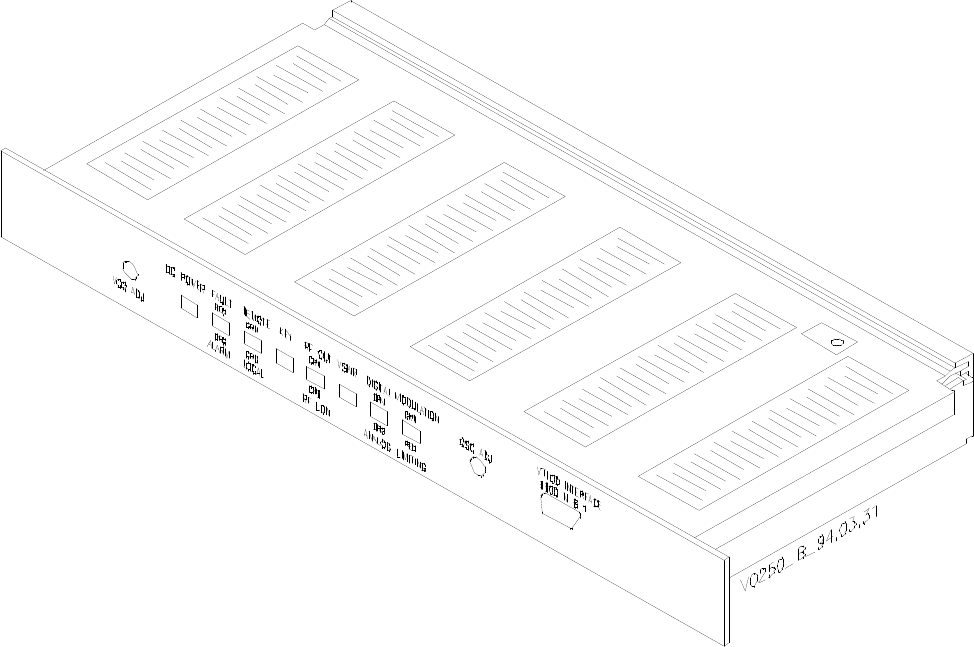
1.3 Exciter Identification
Refer to Figure Figure 1-1, DSP Exciter Isometric View, for an overall view of the
exciter.
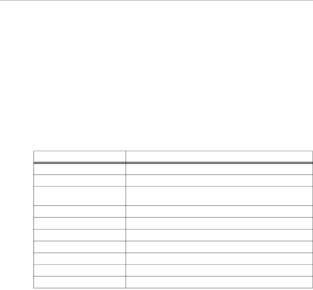
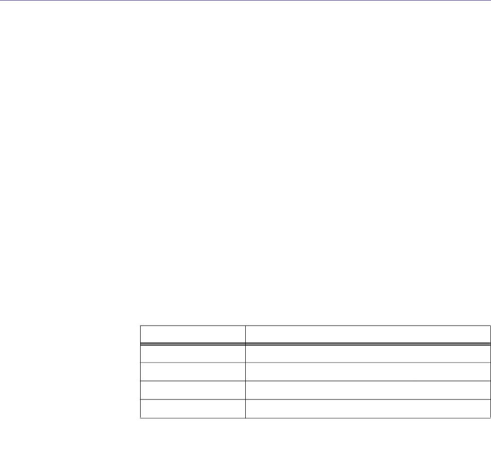
Table 1-1 Manual Contents
section No. and title contents
1 General this section
2 Specifications exciter specifications
3 Descriptions listing of options and assemblies covered, simplified description, physical
description, simplified block theory of operation
4 Installation and Setup exciter installation, setup, and lists of connections
5 Operation list, description, and location of operator controls and indicators
6 Theory of Operation assembly-level description of exciter operation
7 Maintenance exciter maintenance
8 Checkout and Troubleshooting exciter checkout and troubleshooting
9 Removal and Reinstallation procedures for removing and reinstalling exciter and exciter assemblies
10 Options list and discussion of user selectable options
DSP Exciter Glenayre Document Number: 9110.00172
GENERAL Issue 1, Rev. I: 01/15/97
Page: 1-2 Copyright © 1997 Glenayre Print Date: 02/19/97
v0250.hgl
Figure 1-1 DSP Exciter Isometric View

Glenayre Document Number: 9110.00172 DSP Exciter
Issue 1, Rev. I: 01/15/97 SPECIFICATIONS
Print Date: 02/19/97 Copyright © 1997 Glenayre Page: 2-1
sec_2
2 SPECIFICATIONS
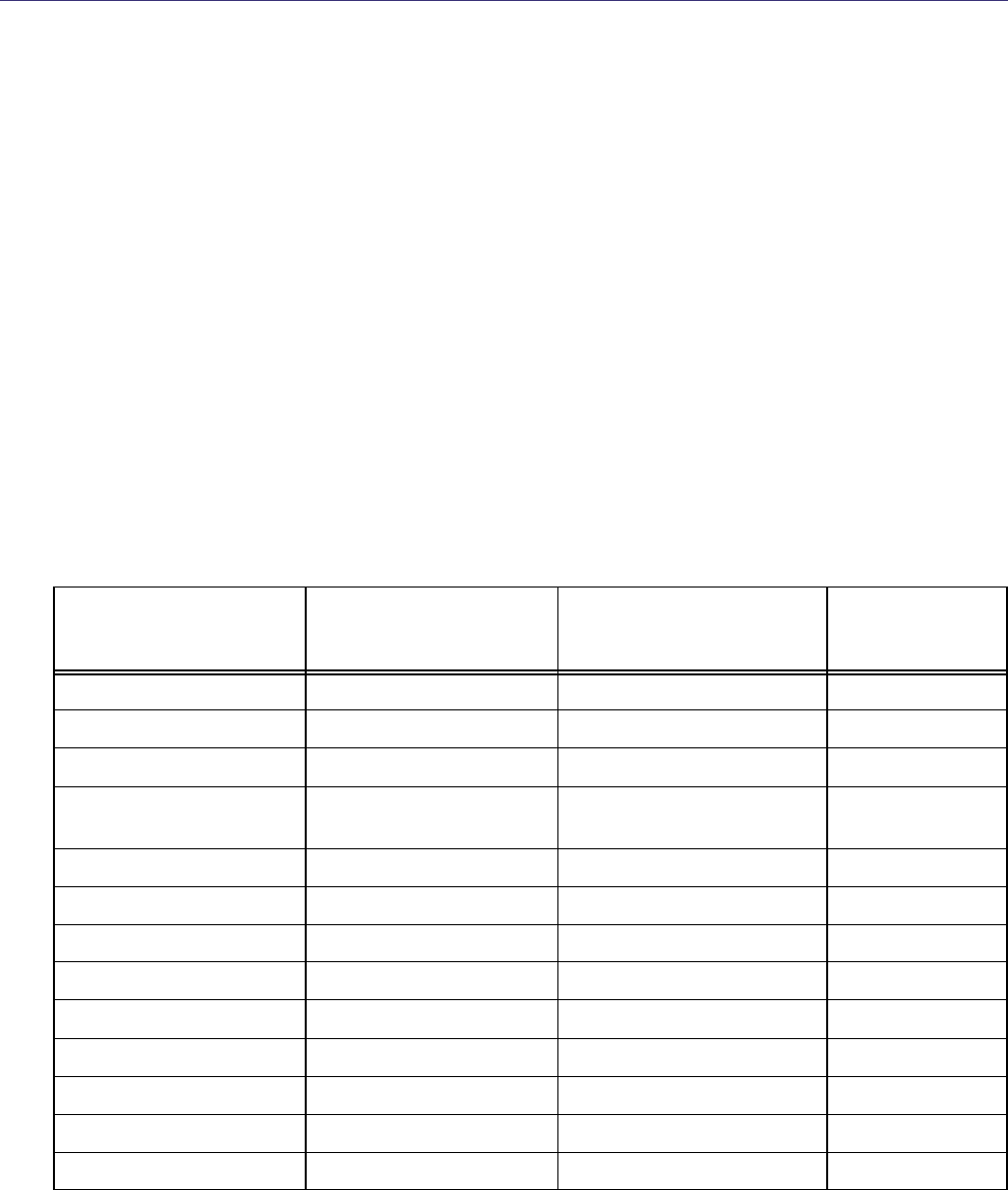
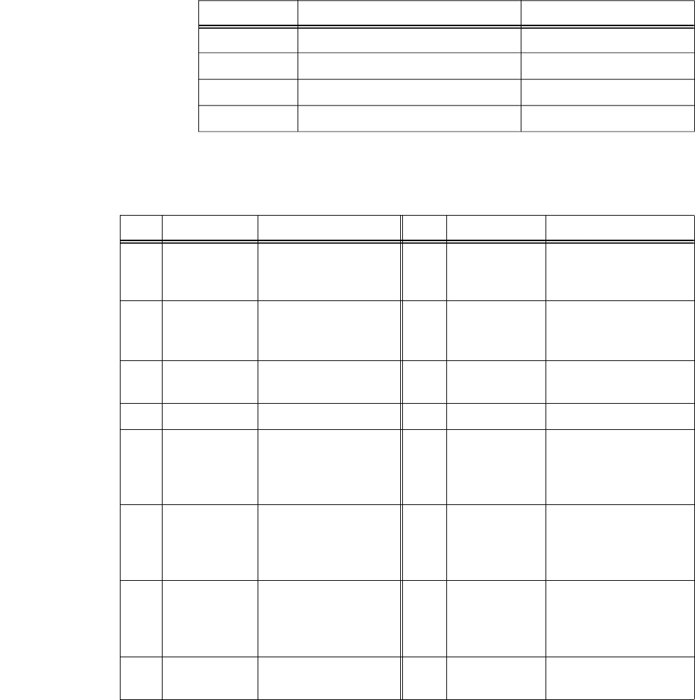
Refer to Table 2-1, Exciter Specifications, which lists the DSP exciter specifications.
Where possible, EIA or I-EIS A measuring methods were used in determining specifica-
tions. Note that some specifications are not addressed by either set of standards or the
prescribed methods were impractical.
Table 2-1 Exciter Specifications
characteristic condition specification
adjacent-channel noise 25-kHz channel spacing, in analog mode -85 dBc
25-kHz channel spacing, in FSK mode -75 dBc
alternate channel noise 25-kHz channel spacing -95 dBc
spurious -90 dBc
operating frequency range determined by installed VCO/RF board refer to Table 3-1
RF output power keyed 250 mW nominal
carrier frequency stability steady state, -30° to
+60° C
10-MHz reference, int=0.005 ppm/yr,
ext=0.1 ppm/yr
FSK frequency/modulation stability relative to carrier frequency stability +/- 10 Hz max
FSK adjustment accuracy +/- 10 Hz
analog offset resolution 1 Hz
number of channels up to 8, depending on interface board and
controller
frequency spread 3 MHz at 900 MHz (12 MHz wideband
option)
7.5 MHz at 450 MHz
5 MHz at 150 MHz
audio input level -25 to +10 dBm
impedance with transformer 600 ohm or 5 kohms balanced
audio response flat, 50 to 2800 Hz; not referenced to 1
kHz; 60% deviation
+/-0.5 dB
preemphasized 6 dB per octave, 300 to
3000 Hz; 60% deviation
+/-0.75 dB

DSP Exciter Glenayre Document Number: 9110.00172
SPECIFICATIONS Issue 1, Rev. I: 01/15/97
Page: 2-2 Copyright © 1997 Glenayre Print Date: 02/19/97
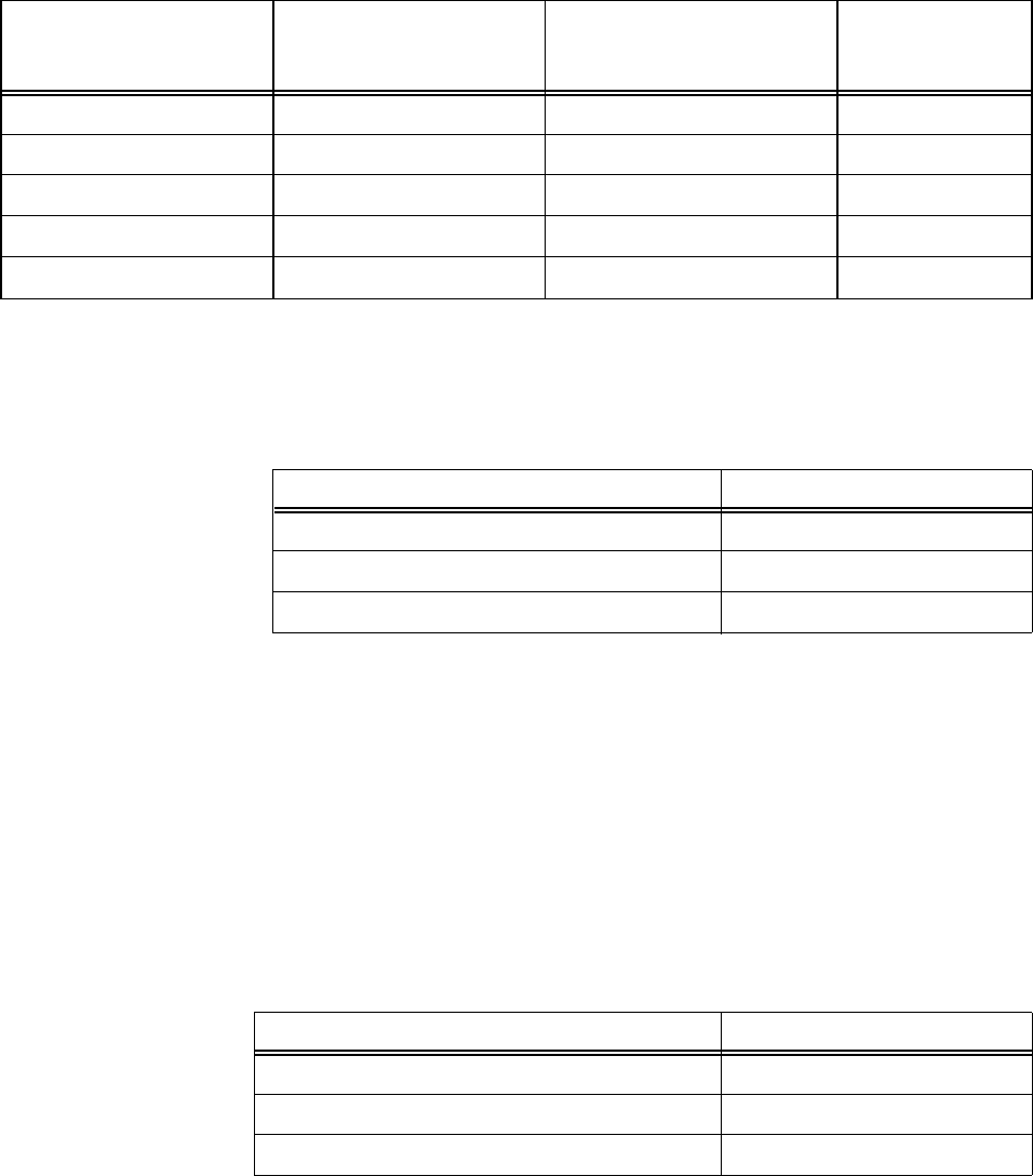
audio distortion (1-kHz reference at
60% deviation)
25-kHz channel spacing less than 1.5%
audio response (tracking between
units)
level 0.1 dB max
delay 2 usec max
FM hum and noise (1-kHz reference
at 60% deviation)
25-kHz spacing flat, 15-kHz bandwidth -40 dB
25-kHz channel spacing preemphasized,
300 to 3000 Hz
-55 dB
AM hum and noise standard -34 dB
modulation types analog, 2-level FSK, 4-level FSK avail-
able with some interfaces
channel spacing 6.25 kHz
audio-backward compatibility standard
emissions FCC 15K0F2D, 16K0F1D, 16K0F3E
power requirement 22-29 Vdc less than 3 A
humidity noncondensing 0 to 95% relative
external 10-MHz reference input level 2Vp-p min
impedance 50 ohms
spurious above 8 MHz -65 dBc max
spurious below 8 MHz -50 dBc max
weight 4.8 lb (2.2 kg)
dimensions 8.75 in (22.25 cm) d x 19 in (48.25 cm) w
x 1.75 in (4.5 cm) h
temperature range operating (nonderated) -30° to +60° C
storage -55° to +70° C
maximum elevation to 10,000 ft (3050 m)
Table 2-1 Exciter Specifications (continued)
characteristic condition specification
Glenayre Document Number: 9110.00172 DSP Exciter
Issue 1, Rev. I: 01/15/97 DESCRIPTION
Print Date: 02/19/97 Copyright © 1997 Glenayre Page: 3-1
sec_3
3 DESCRIPTION
3.1 Introduction
The DSP exciter contains a microprocessor that allows remote or local control of the exciter
and consolidates logic for varying degrees of PA control and monitoring through a video
display terminal (VDT). Operating characteristics of the exciter are controlled by the
selection of hardware options. It is frequency selectable by specifying the appropriate
internal frequency determining hardware and software. It is also capable of communicating
with several operating protocols through the proper selection of interface boards.
3.2 Physical Description
The exciter front panel of one RU (1.75 in) in height contains eight LEDs, two adjustments,
and one connector (also see section 5). The exciter chassis is nine inches deep and contains
three circuit boards and space for an oscillator (not used with some controllers).
Refer to Table 3-1, Part Numbers of VCO/RF Amplifier Boards, which shows
subassemblies used for various transmitter operating ranges.
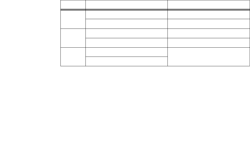
Table 3-1 Part Numbers of VCO/RF Amplifier Boards
transmitter model VCO/RF-amplifier board
frequency band (MHz) VCO board assembly part
No.
control board
assembly part
No.
GL-T85/8601 929-941 263-0082-072 265-0082-001
936-948 263-0082-070 265-0082-001
924-936 263-0082-069 265-0082-001
GL-T85/8600 900-960 (wb) 263-0082-051/052/053/054/
055/062
265-0082-024/032
948-960 263-0082-055 265-0082-001
936-948 263-0082-054 265-0082-001
929-941 263-0082-068 265-0082-001
924-936 263-0082-053 265-0082-001
GL-T8541 445-470 263-0084-003 not yet available
GL-T83/8531 320-330 263-0082-049 265-0082-001
GL-T83/8521 275-285 263-0082-047 265-0082-001
GL-T84/8611 167-175 2100.00094 265-0082-024
162-172 2100.00093 265-0082-024
DSP Exciter Glenayre Document Number: 9110.00172
DESCRIPTION Issue 1, Rev. I: 01/15/97
Page: 3-2 Copyright © 1997 Glenayre Print Date: 02/19/97
Refer to Table 3-2, Part Numbers of Interface Boards.
Refer to Figure 3-1, DSP Exciter Rear View, which shows the exciter rear panel. The
back panel contains three BNC-type connectors J3/J7/J8, a DB-15 connector J6, and a
terminal board TB1 as standard items. Other back panel connectors vary depending on
which interface and I/O boards are installed. Figure 3-2, DSP Exciter Top View with
Internal Controls and Indicators, shows a top view of the exciter with its cover removed.
Refer to Table 3-3, Part Numbers of Interface I/O Boards, which shows interface and I/
O board part numbers. The I/O boards comprise the means to connect various controllers
to the DSP exciter
..
157-167 2100.00092 265-0082-024
152-162 2100.00091 265-0082-024
147-157 2100.00090 265-0082-024
142-152 2100.00089 265-0082-024
138-148 2100.00088 265-0082-024
Table 3-2 Part Numbers of Interface Boards
DSP exciter-to-controller interface boards interface board part No.
QT-1000 interface bd 265-0082-007
standard Interface bd 263-0082-036
I20 interface bd 265-0082-032
Table 3-3 Part Numbers of Interface I/O Boards
interface I/O board (control type) interface I/O board part No.
QT-1000 Interface I/O bd 261-0082-003
Standard Interface I/O bd 261-0082-004
I20 Interface I/O bd pending
Table 3-1 Part Numbers of VCO/RF Amplifier Boards (continued)
transmitter model VCO/RF-amplifier board
frequency band (MHz) VCO board assembly part
No.
control board
assembly part
No.
Glenayre Document Number: 9110.00172 DSP Exciter
Issue 1, Rev. I: 01/15/97 DESCRIPTION
Print Date: 02/19/97 Copyright © 1997 Glenayre Page: 3-3
sec_3
3.3 Simplified Block-Diagram Description
Refer to Figure 3-3, DSP Exciter Simplified Functional Diagram, in the following
discussion. Inputs from the transmitter controller usually are one or two data bits, two
channel-select bits, and keying input. Outputs to the controller are keying output indicator,
various fault outputs, forward-power sample, and reflected-power sample.
Table 3-4 Assembly and Control Board Numbers
exciter assembly No. control board No.
(wb) 2100.00085 265-0082-032
265-0082-021 265-0084-024
DSP Exciter Glenayre Document Number: 9110.00172
DESCRIPTION Issue 1, Rev. I: 01/15/97
Page: 3-4 Copyright © 1997 Glenayre Print Date: 02/19/97
v0343.hgl
Figure 3-1 DSP Exciter Rear View
Glenayre Document Number: 9110.00172 DSP Exciter
Issue 1, Rev. I: 01/15/97 DESCRIPTION
Print Date: 02/19/97 Copyright © 1997 Glenayre Page: 3-5
sec_3
v0344.hgl
Figure 3-2 DSP Exciter Top View
with Internal Controls and Indicators
DSP Exciter Glenayre Document Number: 9110.00172
DESCRIPTION Issue 1, Rev. I: 01/15/97
Page: 3-6 Copyright © 1997 Glenayre Print Date: 02/19/97
v0251.hgl
Figure 3-3 DSP Exciter Simplified Functional Diagram
Glenayre Document Number: 9110.00172 DSP Exciter
Issue 1, Rev. I: 01/15/97 INSTALLATION AND SETUP
Print Date: 02/19/97 Copyright © 1997 Glenayre Page: 4-1
sec_4
4 INSTALLATION AND SETUP
4.1 Precautions and Hazards
Caution
PC boards within this assembly use
static-sensitive components. Follow
IC-handling precautions.
Caution
The exciter contains internal memory which is
used to characterize exciter operation. Upon
exciter replacement, ensure that replacement
exciter contains appropriate items in its memory.
4.2 Test Equipment and Tools Required
Table 4-1, Test Equipment Required, lists required test equipment. Common hand tools
may also be required for most procedures.
4.3 Component and Adjustment Locations
Figure 3-3, DSP Exciter Simplified Functional Diagram, shows the location of assem-
blies, internal user-adjustable controls, and I/O locations. Note that most adjustments are
performed via the front-panel VT100 interface.
4.4 Installation
4.4.1 Inspection
Inspect exciter to ensure air flow is not obstructed and cables and wires are securely
fastened to their respective connectors.
Table 4-1 Test Equipment Required
item description
tuning tool Johanson 8777 or equivalent
RF power meter Bird model 8327 or equivalent with appropriate RF adapters
voltmeter Fluke model 77 DVM or equivalent
RF dummy load 50-ohm load

DSP Exciter Glenayre Document Number: 9110.00172
INSTALLATION AND SETUP Issue 1, Rev. I: 01/15/97
Page: 4-2 Copyright © 1997 Glenayre Print Date: 02/19/97
4.4.2 Power Requirement
The DSP exciter, when used as a component of a transmitter, draws its power from system
wiring. Current draw is less than three amperes at 22 to 29 volts. It is normally powered by
the transmitter power supply but can be powered by an auxiliary supply.
4.4.3 Input/Output Connections
Figure 3-3, DSP Exciter Simplified Functional Diagram, shows the locations of I/O
connectors; Table 4-2, DSP Exciter I/O Connectors, lists I/O connectors and describes
their functions. Normally the exciter is delivered as part of an entire transmitter and has
already been installed in a rack, with all connections already made, except for connections
to equipment that was not installed in the rack before shipment. If I/O connections are
required, refer to the system-interconnect diagram and other instructions in the transmitter
manual.
4.4.4 Signal Functions
See Table 4-2, DSP Exciter I/O Connectors, which references other tables that describe
pin-by-pin functions of multipin connectors. Figure 4-1, DSP Exciter/PA Control
Circuit Boards Interconnection Diagram, shows interconnections among internal
assemblies.
Table 4-2 DSP Exciter I/O Connectors
stencil/connector description additional
detail
VT100 INTERFACE: J3 VT100 interface to VDT (front) Table 4-3
RF OUT: J3 RF out, on frequency Figure 6-1
QT-1000 interface I/O J4 interface to QT-1000 interface board Table 10-1
QT-1000 interface I/O J5 DB-9 connector, to receiver Table 10-2
standard interface I/O J4 interface to standard interface I/O board Table 10-1
GL-C2000 interface I/O J4 interface to GL-C2000 interface I/O board
PA CONTROL: J6 connects to PA Table 4-4
ISOLATOR IN: J7 VSWR input from PA Figure 3-1
10 MHZ IN: J8 external reference input from interface Figure 3-1
+26 VDC: TB1 exciter input power, +22-29 Vdc Figure 3-1
Glenayre Document Number: 9110.00172 DSP Exciter
Issue 1, Rev. I: 01/15/97 INSTALLATION AND SETUP
Print Date: 02/19/97 Copyright © 1997 Glenayre Page: 4-3
sec_4
4.4.5 Switches and Jumpers
Figure 3-2, DSP Exciter Top View with Internal Controls and Indicators, shows the
locations of user-adjustable switches and jumpers. Refer to Table 4-5 for a list of software
related jumper positions found on the exciter/control board. No switches are available to
maintenance personnel.
Table 4-3 VT100 Interface Connector J3 Pin Assignments
J3-X (front) signal description
2 TXD transmit data line
3 RXD receive data line
5GND ground
1,4,6,7,8,9 not used
Table 4-4 Control Board Connector J6 Pin Assignments
J6-X signal description J6-X signal description
1 A/D1+ multiplex analog
input from PA No. 1
multiplexer
9 A/D2+ multiplex analog input
from PA No. 2 multi-
plexer
2 A/D3+ multiplex analog
input from PA No. 3
multiplexer
10 A/D4+ multiplexed analog input
from PA No. 4 multi-
plexer
3 AGC REF+ GC reference voltage
output to PA, 1-12 Vdc
11 PA FAULT PA fault input, HI=fault
4 PA GROUND no connection 12 PA GROUND no connection
5 PA GROUND no connection 13 INPUT
SELECT 1
one of four select outputs
to PA multiplexers,
LO=20 digit enabled for
mux input decoder
6 INPUT
SELECT 2/
KEY OUT
one of four select out-
puts to PA multiplexers,
LO=21
14 INPUT
SELECT 3
one of four select outputs
to PA multiplexers,
LO=22 digit enabled for
mux input decoder
7 INPUT
SELECT 4/
KEY OUT
one of four select out-
puts to PA multiplexers,
not used
15 AUX LATCH
ENABLE
latch-enable output to PA
multiplexers, LO=mux
input decoder reads the
three select inputs
8 REF SAMPLE reflected power sample
input from PA
DSP Exciter Glenayre Document Number: 9110.00172
INSTALLATION AND SETUP Issue 1, Rev. I: 01/15/97
Page: 4-4 Copyright © 1997 Glenayre Print Date: 02/19/97
4.5 Setup
Note
When doing a setup for a wideband DSP exciter, the net channel change
time must be set for 300 ms.
Refer to the DSP exciter VDT Menus and user manual for transmitter-control setup infor-
mation. All setup is done via the front-panel VT100 interface.
4.6 Ultimate Disposition
Caution
This equipment may contain hazardous materials.
Check with the local EPA or other environmental
authority before disposing of this equipment.
Table 4-5 Exciter Control Board Jumper Positions
Jumper pre version 2.10 software version 2.10 software
JW1 set to A for external 10 MHz oscillator set to A for external 10 MHz oscillator
set to B for internal 10 MHz oscillator set to B for internal 10 MHz oscillator
JW2 set to A for password protection set to A for password protection
set to B to bypass password protection set to B to bypass password protection
JW3 set to A for external VSWR protection always set to B (for internal and/or ex-
ternal VSWR protection)
set to B for internal VSWR protection
Glenayre Document Number: 9110.00172 DSP Exciter
Issue 1, Rev. I: 01/15/97 INSTALLATION AND SETUP
Print Date: 02/19/97 Copyright © 1997 Glenayre Page: 4-5
sec_4
v0164.hgl
Figure 4-1 DSP Exciter/PA Control Circuit Boards
Interconnection Diagram
DSP Exciter Glenayre Document Number: 9110.00172
INSTALLATION AND SETUP Issue 1, Rev. I: 01/15/97
Page: 4-6 Copyright © 1997 Glenayre Print Date: 02/19/97

Glenayre Document Number: 9110.00172 DSP Exciter
Issue 1, Rev. I: 01/15/97 OPERATION
Print Date: 02/19/97 Copyright © 1997 Glenayre Page: 5-1
sec_5
5 OPERATION
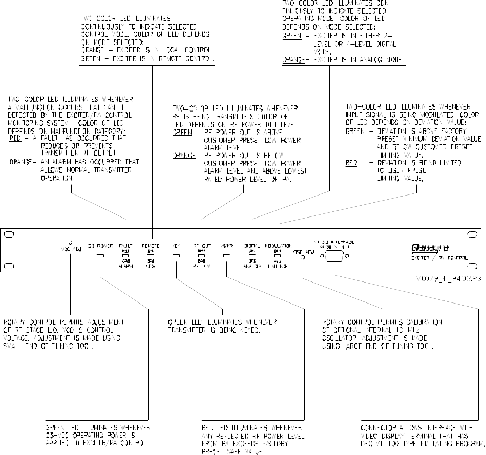
5.1 Front-Panel Controls and Indicators
Refer to Figure 5-1, Front-Panel Controls and Indicators, which shows and describes
front-panel indicators. The DSP exciter contains no front-panel controls. A front-panel
access to VCO adjustment is for maintenance purposes only.
5.2 Operating Instructions
The transmitter controller operates the exciter and transmitter in an unattended manner
during normal system operation. The VT100 interface with a VDT enables the maintenance
technician to perform maintenance and observe operational parameters. Refer to the DSP
exciter VDT Menus and user manual for detailed operating information.
DSP Exciter Glenayre Document Number: 9110.00172
OPERATION Issue 1, Rev. I: 01/15/97
Page: 5-2 Copyright © 1997 Glenayre Print Date: 02/19/97
v0079.hgl
Figure 5-1 Front-Panel Controls and Indicators

Glenayre Document Number: 9110.00172 DSP Exciter
Issue 1, Rev. I: 01/15/97 THEORY OF OPERATION
Print Date: 02/19/97 Copyright © 1997 Glenayre Page: 6-1
sec_6
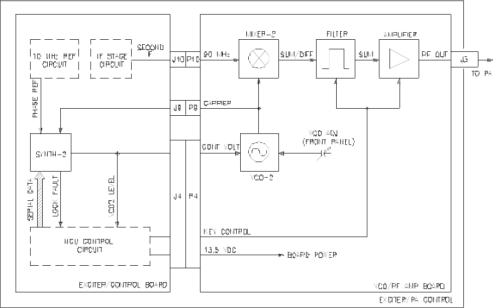
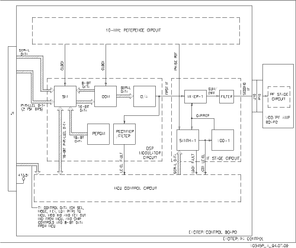
6 THEORY OF OPERATION
6.1 Exciter/PA Control
Refer to Figure 6-1, DSP Exciter RF Stage Functional Diagram, which describes the
signal flow in the DSP exciter with the transmitter controller interface. The following major
paragraphs describe the operation of the major items within the figure. Additional detailed
figures are referenced, as required.
6.1.1 Reference Source
The ten-MHz reference signal is provided by the transmitter controller or by an optional
internal reference oscillator. All other inputs and outputs, except for RF output, are routed
through the interface board.
6.1.2 Main Circuit Frequencies
The VCO/RF amplifier board installed determines the frequency for the RF output.
Table 6-1, Exciter RF/Main Circuit Frequencies lists VCO/RF amplifier board frequen-
cies and the corresponding exciter/output frequencies.
6.1.3 Controller Interface Connector Functions
Refer to Table 4-2, DSP Exciter I/O Connectors and subsequent tables for a pin-by-pin
description of signal functions. The exciter interfaces with the transmitter controller
through the exciter interface I/O board. Connector P4 on the internal interface board
connects directly to J4 on the exciter. Alarm signals, consisting of transmitter alarm, fault,
and status signals, are supplied directly to the transmitter controller.
Table 6-1 Exciter RF/Main Circuit Frequencies
exciter
output
frequency
(MHz)
first IF
frequency
(kHz)
second IF
frequency
(MHz)
VCO-1
frequency
(MHz)
VCO-2
frequency
(MHz)
900-960 100 90 89.9 810-870
445-470 100 90 89.9 355-380
275-330 100 90 89.9 365-420
130-180 100 90 89.9 220-270
DSP Exciter Glenayre Document Number: 9110.00172
THEORY OF OPERATION Issue 1, Rev. I: 01/15/97
Page: 6-2 Copyright © 1997 Glenayre Print Date: 02/19/97
v0123.hgl
Figure 6-1 DSP Exciter RF Stage Functional Diagram

Glenayre Document Number: 9110.00172 DSP Exciter
Issue 1, Rev. I: 01/15/97 THEORY OF OPERATION
Print Date: 02/19/97 Copyright © 1997 Glenayre Page: 6-3
sec_6
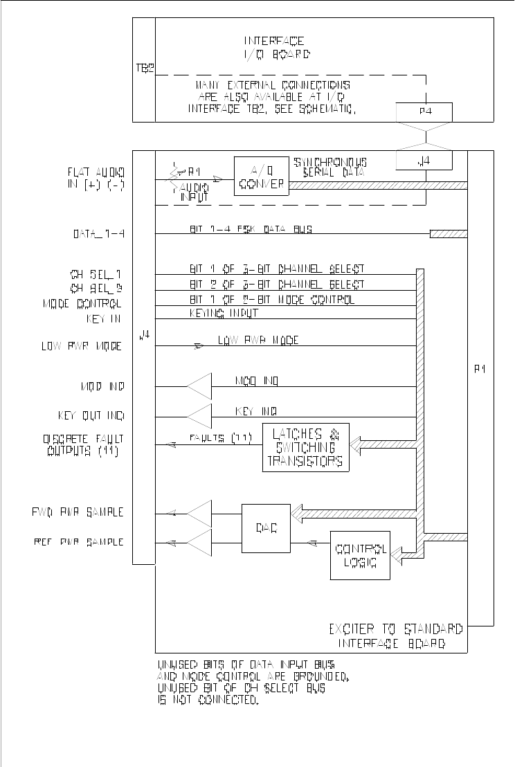
6.2 Interface to Controller
6.2.1 General
The controller interface is the portion of exciter circuitry that connects the transmitter
controller to the exciter. The interface board dictates what kind of transmitter controller
may operate the transmitter. The transmitter can be operated through one of several control-
lers depending on which interface board is installed in the exciter. The internal interface
board may also exhibit an external I/O board.
Control commands from the transmitter controller are connected through the interface
circuit. This circuit supplies remote control to the microcontroller unit (MCU) control
circuit. The VT-100 VDT supplies local control. The MCU control circuit generates all
control signals for the other circuits, and monitors their status. The MCU control circuit
reports status back to the VT-100 VDT and the interface circuit, which supplies the status
to the transmitter controller.
6.2.2 Interface Conversion Functions
Some signals exchanged between the controller and the exciter originate with a format,
voltage, or requirement incompatible with their destination. The interface performs any
signal conversions necessary to provide compatibility between the controller and the
exciter. None, some, or all of the following conversion functions may be done by any one
particular interface board.
6.2.2.1 Analog-Mode A/D Conversion
The DSP modulator circuit reads synchronized serial data for its analog mode input signal.
if the transmitter controller provides an analog signal, the controller interface converts the
analog to the appropriate data form for the DSP. The analog (FLAT AUDIO+, -) terminates
across a balanced input circuit that also provides a level adjustment. The adjustment, when
properly set by the AUDIO INPUT ADJUST pot through the exciter cover, provides analog
to an A/D converter at the optimum zero-dBm level. The A/D converts the analog into
serial data, which is applied to the DSP through a synchronous data link. A synchronous
data link is characterized by an exchange of pulse streams for timing purposes. The A/D
converter is clocked by a pulse generator circuit driven by the ten-MHz reference circuit.
6.2.2.2 FSK-Data-Bit Strapping
The DSP modulator circuit can read up to four bits for its digital FSK mode input signal. If
the controller provides only bit 1 (DATA 1), operation in the four-level mode or higher is
precluded. Bits 2 through 4 (DATA2 through DATA4) are available as FSK data inputs;
whether they are used or not is a function of the particular controller interface used and the
transmitter controller. Refer to Section 10. The controller interface disables unused bits by
ground straps.
DSP Exciter Glenayre Document Number: 9110.00172
THEORY OF OPERATION Issue 1, Rev. I: 01/15/97
Page: 6-4 Copyright © 1997 Glenayre Print Date: 02/19/97
6.2.2.3 Channel-Select-Bit Strapping
The MCU control circuit reads three bits to determine the remotely selected channel. If the
controller provides only bits 1 and 2 (CH SEL 1, 2), the controller can command only four
channels. The operation of bit 3 is a function of the controller interface. Refer to Section 10.
6.2.2.4 Mode-Select-Bit Strapping
The MCU control circuit reads two bits to determine the remotely selected mode. If the
controller provides only bit 1 (MODE CONTROL), the controller can command only two
transmitter modes. The operation of bit 2 is a function of the controller interface. Refer to
Section 10. If the controller interface does not use bit 2, it straps it to ground (low).
6.2.2.5 Power Sample D/A Conversion
The controller reads sample voltages for its forward and reflected power sample inputs,
which are stored as data in the MCU control circuit. In some cases the controller interface
converts the data to voltages of the appropriate range for the controller. Data from the MCU
representing the forward and reflected powers is written into a dual D/A converter, which
converts the data into two proportional dc voltages, which are applied to the controller.
Control logic gates ensure that data is written to the proper half of the D/A converter.
6.3 DSP Modulator
6.3.1 General
The DSP modulator circuit converts the data into the first IF signal, which is fully modu-
lated. The IF stage circuit converts the first IF signal into the second IF signal. The RF stage
circuit converts the second IF signal into the RF output. Ten MHz is used as frequency
reference by each conversion stage. The DSP modulator is the portion of exciter circuitry
between the controller interface and the IF stage. The DSP modulator uses digital signal
processing to modulate and up-convert the paging information into the first IF signal. The
modulation type depends on the transmitter operating mode. The IF stage is the portion of
exciter circuitry between the DSP modulator and the RF stage. The IF stage uses hetero-
dyne mixing to generate the optimum second IF signal frequency, which depends on the
requirement of the VCO/RF amplifier board installed. The MCU control circuit is the
command and control hub of the transmitter. The type of control software depends on the
transmitter frequency and power output. The following text describes main exciter circuitry
that works for all software programs, modulation schemes, and IF signal frequencies.
Figure 6-2, DSP Exciter MCU Circuit Functional Diagram shows additional details.
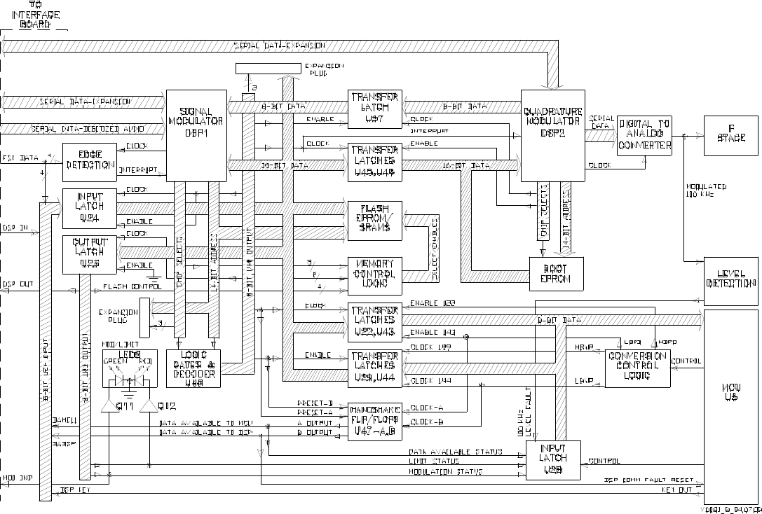
6.3.2 DSP Modulator Signal Flow
Refer to Figure 6-2, DSP Exciter MCU Circuit Functional Diagram, in the following
discussion. The inputs that provide the paging information to the DSP modulator circuit are
digitized audio and FSK data, supplied by the controller interface circuit through connector
pair P1/J1. Digitized audio arrives as serial data. FSK data arrives as parallel data. The DSP
modulator circuit processes the digitized audio in the analog mode or the FSK data in the
digital mode. The result of this processing is the exciter’s first IF signal, which is applied

Glenayre Document Number: 9110.00172 DSP Exciter
Issue 1, Rev. I: 01/15/97 THEORY OF OPERATION
Print Date: 02/19/97 Copyright © 1997 Glenayre Page: 6-5
sec_6
to the IF stage circuit. To produce the first IF signal, the DSP modulator contains two DSPs
(a signal modulator and a quadrature modulator), a digital-to-analog converter, and a read-
only memory. The following text describes these four components and their signal flow.
6.3.2.1 Digital Signal Modulator
The signal modulator (SM) generates modulation that contains the paging information,
which is supplied by digitized audio or FSK data. The digitized audio is input into a serial
input port. An external edge detector is required to input the FSK data. The SM converts
one of the data inputs into a modulated signal, which is mathematically represented within
the SM as a vector signal, defined by its rectangular coordinates. These coordinates,
commonly known as I and Q, are supplied to the digital quadrature modulator as 16-bit
parallel data. The modulated signal output from the SM depends on the following signal
characteristics:
•modulation scheme
•frequency response or rise time
•input logic or data inversion
•deviation level or bandwidth
•offset from carrier frequency
•analog gain and deviation limit
The SM also performs all communications between the DSP modulator circuit and the
MCU control circuit. These communications are through the SM 16-bit parallel data port.
External input and output latches expand the capabilities of this port. Control inputs consist
of commands such as reset, request status, set paging signal parameter, change mode, and
boot program. Requested status outputs consist of current mode, deviation levels, input
level, input gain, modulation detected, and current polarity. Nonrequested status outputs
indicate the existence of analog limiting and modulation.
6.3.2.2 Digital Quadrature Modulator
The digital quadrature modulator (DQM) performs interpolation and up-conversion of the
modulated signal. The modulated signal input to the DQM is applied by the SM as I and Q
components (16-bit parallel data). The DQM performs trigonometric computations at a
much higher sampling rate, which determines the first IF signal value and frequency. The
modulated signal output from the DQM is supplied from its serial data port to the D/A
converter.
6.3.2.3 Digital-to-Analog Converter
The digital input to the digital-to-analog (D/A) converter is the modulated signal from the
DQM. This data arrives as serial data. The analog output from the D/A converter is the first
IF signal. In addition to the IF stage circuit, the first IF signal is supplied to the MCU
control circuit, where it is rectified and filtered to generate fault logic.
DSP Exciter Glenayre Document Number: 9110.00172
THEORY OF OPERATION Issue 1, Rev. I: 01/15/97
Page: 6-6 Copyright © 1997 Glenayre Print Date: 02/19/97
v0 083.hgl7
Figure 6-2 DSP Exciter MCU Circuit Functional Diagram

Glenayre Document Number: 9110.00172 DSP Exciter
Issue 1, Rev. I: 01/15/97 THEORY OF OPERATION
Print Date: 02/19/97 Copyright © 1997 Glenayre Page: 6-7
sec_6
6.3.2.4 Read-Only Memory
A programmable and erasable read-only memory (PEROM) stores the modulator programs
for both DSPs. These programs are transferred to the SM when the exciter is booted up
(powered up), then the SM transfers the program to the DQM. The nonvolatile PEROM
retains its program for years. Its memory may be individually reprogrammed without
erasing the entire chip.
6.4 IF Stage
Refer to Figure 6-1, DSP Exciter RF Stage Functional Diagram. The input to the IF
stage is the first IF signal, which is supplied by the DSP modulator circuit. The first IF
signal carries all the paging information on an intermediate carrier frequency. The IF stage
performs direct up-conversion of the first IF signal to create the second IF signal, which
carries the same paging information as the first IF signal, but on a higher carrier frequency.
The second IF signal is applied to the RF stage through connector pair J10/P10. To produce
the second IF signal, the IF stage contains mixer-1 and filter circuits. Supporting these
circuits are VCO-1 and synthesizer-1 circuits. Figure 6-2, DSP Exciter MCU Circuit
Functional Diagram, and Figure 6-3, DSP Exciter-to-Controller Functional
Diagram, show additional detail.
6.4.1 Mixer-1
Mixer-1 is the first heterodyne mixer. Inputs to mixer-1 are a modulated IF and a carrier.
The modulated IF input is the first IF signal. The carrier input is supplied by VCO-1. The
output from mixer-1 consists of two modulated carriers that are sums and difference
frequencies of the inputs. These two frequencies are applied to the filter circuit.
6.4.2 Filter
The filter is centered at the second IF signal frequency with a 45-kHz bandwidth. The input
to the filter consists of two modulated carriers. These are sum and difference frequencies
supplied by mixer-1. The output from the filter is only the sum frequency. This modulated
output is the second IF signal.
6.4.3 VCO-1
VCO-1 is the local oscillator for the IF stage. The input to VCO-1 is a dc control voltage.
This voltage controls VCO-1 carrier frequency and is supplied by synthesizer-1. The output
from VCO-1 is a sine-wave carrier. The output is applied to mixer-1.
6.4.4 Synthesizer-1
Synthesizer-1 controls VCO-1 carrier frequency by means of a phase-locked loop (PLL).
PLL inputs are a carrier and a phase reference. The reference input is a ten-MHz carrier
supplied by the ten-MHz reference circuit. The carrier input is from VCO-1. The PLL
output is a dc control voltage. This voltage, set to cause the VCO-1 carrier to lock phases
with the reference, is supplied to VCO-1.
DSP Exciter Glenayre Document Number: 9110.00172
THEORY OF OPERATION Issue 1, Rev. I: 01/15/97
Page: 6-8 Copyright © 1997 Glenayre Print Date: 02/19/97
Synthesizer-1 also performs all communications between the IF stage circuit and the MCU
control circuit. A control input specifies the VCO-1 carrier frequency; this data is received
over a serial data link when the exciter is booting or changing channels. Status outputs are
a lock fault and a VCO1 level. The lock fault indicates loss of the carrier/reference phase
lock. The VCO1 level is the VCO-1 control voltage.
6.5 MCU
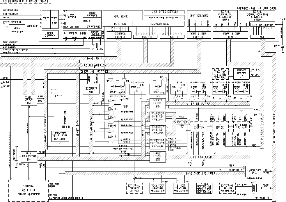
Refer to Figure 6-4, DSP Exciter Detailed Functional Diagram. Control outputs are
supplied by the MCU control circuit to the other functional circuits. Likewise, status inputs
are applied to the MCU control circuit from the other functional circuits. Discussions of
these control and status signals are included with the information on the other major func-
tional circuits. To interface these control and status signals, the MCU control circuit
contains an MCU, D/A converter, 8/16 bit converter, read-only memory, and a VSWR-fault
detector. To light the front-panel LEDs, the MCU control circuit contains a bank of PNP
switching transistors.
Refer to Figure 6-2, DSP Exciter MCU Circuit Functional Diagram, in the following
text which describes this circuitry and its signal flow.
6.5.1 Microcontroller Unit (MCU)
The MCU contains a central processing unit (CPU), memories, peripherals, and other
hardware on a single chip. The primary internal functions of the MCU and their application
in the exciter are described in the following list.
•An eight-bit remote input port accepts discrete low power mode, emission mode, keyline,
and channel selects from the controller interface circuit. An external edge detector is
required to input the channel selects.
•Interrupt logic stops RF transmission when a fault or reset input is received, e.g. a VSWR
or PA fault.
•An on-board oscillator/clock generator, driven by an external crystal, times internal
MCU functions. A synchronized clock output times external functions.
•The MCU performs most interfacing through a parallel communications link: eight-bit
data bus, sixteen-bit address bus, and a read/write line. External input and output latches
expand the capability of this link.
•An eight-bit input/output port supplies discrete keyline, RF status, and chip select
controls to the exciter and the PA.
•A serial peripheral interface (SPI) supplies synchronous serial frequency data to the IF
stage and RF stage circuits. Individual commands load the program into either IF stage’s
synthesizer-1 or RF stage synthesizer-2.
•An 8-input analog-to-digital (A/D) converter measures voltage inputs from the exciter
and the PA. An external multiplexer expands MCU analog inputs to fifteen.
•A serial communications interface (SCI) exchanges asynchronous serial RS-232 data
with the VT-100 VDT. An external RS-232 driver buffers the MCU data, allowing it to
be exchanged through external connector J3.
•A random-access memory (RAM) temporarily stores transmitter fault and alarm values.

Glenayre Document Number: 9110.00172 DSP Exciter
Issue 1, Rev. I: 01/15/97 THEORY OF OPERATION
Print Date: 02/19/97 Copyright © 1997 Glenayre Page: 6-9
sec_6
•An electrically-erasable read-only memory (EEPROM) permanently stores transmitter
signal parameters.
6.5.2 Digital-to-Analog (D/A) Converter
A D/A converter generates an AGC reference voltage. The D/A converter inputs are data
and select logic. The data, supplied by the MCU when the D/A is selected, represents the
desired transmitter power output. The D/A converter output is an AGC reference voltage.
This voltage represents a level proportional to the desired transmitter power output. The
AGC reference voltage, output through connector J6, is used by the PA to generate an AGC
voltage.
6.5.3 8/16-Bit Converter
An 8/16-bit converter allows the MCU eight-bit data bus to communicate with the 16-bit
data bus of the DSP modulator circuit. The MCU must perform two read or write proce-
dures, a low byte and a high byte, to each one of the DSP modulator circuit. The converter
provides two status outputs to the MCU and the DSP modulator circuit. A data-available-
to-MCU status indicates that the DSP modulator circuit has written data into the converter
that the MCU must read. A data-available-to-DSP status indicates that the MCU has written
data into the converter that the DSP modulator circuit must read. In the event that the DSP
modulator circuit does not read data that the MCU has written, a DSP communications fault
is generated.
6.5.4 Read-Only Memory
A programmable and erasable read-only memory (PEROM) stores the control program for
the transmitter. This program is transferred to the MCU when the exciter is booted up. The
nonvolatile PEROM retains its program for years. Its memory may be individually repro-
grammed without erasing the entire chip.
DSP Exciter Glenayre Document Number: 9110.00172
THEORY OF OPERATION Issue 1, Rev. I: 01/15/97
Page: 6-10 Copyright © 1997 Glenayre Print Date: 02/19/97
v0345l7
Figure 6-3 DSP Exciter-to-Controller Functional Diagram
DSP Exciter Glenayre Document Number: 9110.00172
THEORY OF OPERATION Issue 1, Rev. I: 01/15/97
Page: 6-12 Copyright © 1997 Glenayre Print Date: 02/19/97
v0 081.hgll
Figure 6-4 DSP Exciter Detailed Functional Diagram
Glenayre Document Number: 9110.00172 DSP Exciter
Issue 1, Rev. I: 01/15/97 THEORY OF OPERATION
Print Date: 02/19/97 Copyright © 1997 Glenayre Page: 6-13
sec_6
v0077.hglr
Figure 6-5 DSP Exciter IF-Stage Detailed
Functional Diagram
DSP Exciter Glenayre Document Number: 9110.00172
THEORY OF OPERATION Issue 1, Rev. I: 01/15/97
Page: 6-14 Copyright © 1997 Glenayre Print Date: 02/19/97
6.5.5 VSWR-Fault Detector
The exciter receives a VSWR signal from the PA through connector J7. This signal is a
rectified dc voltage sample generated by the isolator. The voltage sample is monitored by
the MCU to provide the value for the total reflected-power indication. The voltage sample
is also monitored by a fault circuit in the exciter. If a factory-preset voltage is exceeded, the
fault circuit shuts down the transmitter by an interrupt to the MCU.
6.5.6 Alarm Data-to-Logic Conversion
The transmitter controller reads logic alarm inputs; most of these alarms are stored as data
in the MCU control circuit. If the controller interface converts the data to individual logic
signals for the controller, data from MCU control representing the alarms is clocked into a
pair of latches. The latches convert the data into continuous logic signals. These signals and
others control a bank of NPN switching transistors that supply the actual logic signal to the
controller. Control logic gates convert chip controls from the MCU into a clock input for
the latches.
6.6 RF Assemblies
6.6.1 RF Stage Location
Refer to Figure 3-3, DSP Exciter Simplified Functional Diagram, to locate the
assembly. The RF stage circuits are located on two circuit boards, both housed within the
exciter chassis.The exciter/control board is the main circuit board and the VCO/RF
amplifier board is a selected option. The exciter/control board connects to the VCO/RF
amplifier board through three connector pairs: J4/P4, J9/P9, and J10/P10. The VCO/RF
amplifier board also contains BNC connector J3, which extends through the rear panel of
the exciter. This board contains most of the RF stage components inside an RF shield. A
hole in the shield and the front panel provide access to an RF stage adjustment, which is
marked VCO ADJ on the front panel.
6.6.2 RF Assemblies
6.6.2.1 RF Stage Description
The RF stage is the portion of exciter circuitry between the IF stage and RF out and is the
final major functional circuit, the RF stage determines the transmitter RF output frequency,
and dictates the highest and lowest possible RF output frequencies (RF band). The trans-
mitter can be operated at several RF bands, depending on the RF stage circuitry installed in
the exciter.
6.6.2.2 RF Stage Bands
The selected VCO/RF amplifier board determines the RF band of the transmitter. Table 3-
1, Part Numbers of VCO/RF Amplifier Boards, lists the RF bands and the part number
of the board with that RF band.

Glenayre Document Number: 9110.00172 DSP Exciter
Issue 1, Rev. I: 01/15/97 THEORY OF OPERATION
Print Date: 02/19/97 Copyright © 1997 Glenayre Page: 6-15
sec_6
6.6.2.3 RF Stage Signal Flow
Refer to Figure 6-1, DSP Exciter RF Stage Functional Diagram. The input to the RF
stage is the second IF signal, supplied by the IF stage circuit through connector pair J10/
P10. The second IF signal carries the paging information on a modulated carrier at the
exciter’s second intermediate frequency. The RF stage converts the second IF signal into
the exciter’s RF output. This RF output carries the same paging information as the second
IF signal, but on a modulated carrier of radio frequency. The RF output is normally applied
to the PA through connector J3. To produce the RF output, the RF stage contains mixer-2,
a filter, and an amplifier. Supporting these circuits are VCO-2 and synth-2. The following
text describes these five circuits and their signal flow.
6.6.2.3.1 Mixer-2
Mixer-2 is the second heterodyne mixer. Inputs to mixer-2 are a modulated IF and a carrier.
The modulated IF is the second IF signal. The carrier is supplied by VCO-2. Output from
mixer-2 consists of sum and difference frequencies of the inputs. The sum frequency is
centered near the channel carrier, and the difference frequency about twice the second IF
frequency below that. These two modulated RF carriers are applied to the filter circuit.
6.6.2.3.2 Filter
The filter is factory-selected and tuned, with a bandwidth determined by carrier frequency
of the transmitter. The inputs to the filter consist of two modulated RF carriers and a key
control.The two carriers are sum and difference frequencies, supplied by mixer-2. The key
control is supplied by the MCU control circuit through J4/P4. The output from the filter,
supplied when the key control is received, is only the sum frequency. This modulated RF,
centered near the channel on-frequency, is supplied to the amplifier.
6.6.2.3.3 Amplifier
The amplifier provides amplification to the value listed in the specifications as exciter RF
power out. The inputs to the amplifier consist of modulated RF and a key control. The
modulated RF, mixer-2 sum output frequency, is supplied through the filter. Key control is
supplied by the MCU control circuit through J4/P4. Output from the amplifier, supplied
when the key control is received, is an amplified version of the modulated RF. This
amplified output is the exciter RF output.
6.6.2.3.4 VCO-2
VCO-2 is the RF stage local oscillator. Inputs to VCO-2 are a dc control voltage and an
adjustment. Dc control voltage is supplied by synthesizer-2. The adjustment, which varies
the VCO2 control voltage level, is controlled through the front-panel VCO ADJ access.
This control provides the means for VCO-2 to output a carrier frequency that would
otherwise be beyond the range of the control voltage input. The carrier output, always
second IF frequency below the channel carrier frequency, is applied to mixer-2.
DSP Exciter Glenayre Document Number: 9110.00172
THEORY OF OPERATION Issue 1, Rev. I: 01/15/97
Page: 6-16 Copyright © 1997 Glenayre Print Date: 02/19/97
6.6.2.3.5 Synthesizer-2
Synthesizer-2 controls VCO-2 carrier frequency by means of a phase-locked loop (PLL).
PLL inputs to synthesizer-2 are a carrier and a phase reference. The reference is a ten-MHz
carrier supplied by the ten-MHz reference circuit. The carrier is the VCO-2 output. The
PLL output from synthesizer-2 is a dc control voltage. This voltage, set to cause VCO-2 to
lock phases with the reference, is applied to the VCO-2 control input.
Synthesizer-2 also performs all communications between the RF stage circuit and the MCU
control circuit. A control input to synthesizer-2 specifies VCO-2 carrier frequency. This
data is received over a serial data link when the exciter is booting or changing channels.
Status outputs from synthesizer-2 are a lock fault and a VCO2 level. The lock fault
indicates loss of the carrier/reference phase lock. VCO2 level is the VCO-2 control voltage.
6.7 Voltage Regulator Circuit
Refer to Figure 6-4, DSP Exciter Detailed Functional Diagram (center, toward bottom)
in the following discussion. The exciter receives 26-volt operating power through terminal
board TB1. The dc power indicator on the exciter front panel is connected to this input. This
voltage is supplied to a 26-volt bus and is monitored by the MCU. An intermediate
regulator reduces the 26 volts to 16.5 volts, which is supplied to the two final regulators.
One regulator generates 13.5 volts, which is supplied to a 13.5-volt bus and monitored by
the MCU. The other regulator generates 5 volts, which is supplied to a five-volt bus and
monitored by the MCU.

Glenayre Document Number: 9110.00172 DSP Exciter
Issue 1, Rev. I: 01/15/97 MAINTENANCE
Print Date: 02/19/97 Copyright © 1997 Glenayre Page: 7-1
sec_7
7 MAINTENANCE
7.1 Location of Maintenance Procedures
The DSP exciter is central to performing transmitter maintenance. Most maintenance of
electrical assemblies is done via the VT100 interface. Any maintenance procedures which
require adjusting controls within the exciter chassis are listed in this section.
Replace the exciter if it has input power, as indicated by the front-panel LED, but does not
allow the user to make connection via the VT100 interface.
7.2 Test Equipment Required
Table 4-1, Test Equipment Required, lists test equipment required to perform mainte-
nance procedures.
7.3 VCO-2 Adjustment Procedure
Perform the VCO-2 adjustment procedure after installing new VCO/RF amplifier board or
after setting new channel carrier frequency. If the transmitter is to operate at more than one
frequency, perform the multichannel adjustment procedure. If the transmitter is to operate
at only one frequency, perform the single-channel adjustment procedure. Refer to the DSP
exciter VDT manual as necessary.
7.3.1 VCO-2 Multichannel Adjustment Procedure
1. Set up VT-100 VDT and select local control (see VDT manual).
2. Select transmitter channel of lowest frequency if not already selected.
3. Use tuning tool supplied to adjust VCO ADJ control through exciter front panel. Ad-
just for a reading of 4.0 volts (3.5 volts for wideband VCO 263-0082-062), on VCO2
status display.
4. Return transmitter to service.
Procedure is complete.
7.3.2 VCO-2 Single-Channel Adjustment Procedure
This procedure does not apply to wideband option.
1. Set up VT-100 VDT and select local control (see VDT manual).
2. Select transmitter channel of operating frequency if not already selected.
3. Use tuning tool supplied to adjust VCO ADJ control through exciter front panel. Ad-
just for reading of 5.0 Vdc on VCO2 status display.
4. Return transmitter to service.
Procedure is complete.

DSP Exciter Glenayre Document Number: 9110.00172
MAINTENANCE Issue 1, Rev. I: 01/15/97
Page: 7-2 Copyright © 1997 Glenayre Print Date: 02/19/97
7.4 Over-The-Link Downloading
Over-the-link (OTL) code downloading allows C2000 transmitter controller (C2000)
software, alarm matrix setup, and exciter software to be downloaded over the C2000 link
channel.
To properly use OTL downloading, C2000 units must be programmed for the correct
control group, site ID, and unit ID, which are integral to C2000 hardware and software.
When information is downloaded over the link channel, the control group, site IDs and/or
unit IDs that are to receive the code must be specified.
Caution
If the control group, site ID, and unit ID are not
specified, all units in the system accept the
download information. In a mixed system, this can
result in some of the transmitters being off the air.
An example of this would be a GL-T8600 exciter
receiving a GL-T8500 exciter programming code.
The GL-T8600 exciter would not operate with this
software and could result in a site visit to correct
the problem.
Programming of control groups and site IDs is done via the C2000 front port with a local
connection or through a modem from a remote location. The control groups should be setup
as a group of transmitters having the same configuration. For example, all GL-T8500 trans-
mitters could be in one control group and GL-T8600 transmitters be in another. This would
allow one to download exciter software to all GL-T8500 transmitters at one time by
selecting their control group. Any transmitter with a different control group would not
accept the download information.
Site ID must be different for each site location, and is used when downloading information
to a specific site location. If there are multiple units at the same site, the site ID and unit ID
need to be specified to download to a specific unit. If the unit ID is not specified, all units
at that site accept the download.
Unit ID is programmed with a rotary switch in the C2000; it must be different for each
C2000 at a site location. To download one specific unit, both site and unit ID must be
specified for that unit; the unit with that site ID and unit ID is the only one that accepts the
download.
For assistance on how to perform a download, call Glenayre customer support at 800-637-
9181.
7.5 On-The-Fly Channel/Mode Changing
Different paging formats may require different digital deviation and offsets of paging data
on the same RF carrier frequency. In the past, the only way to meet the different deviation
requirements on the same frequency was to program two different channels for the same
RF carrier frequency and then program those same two channels for a different digital
Glenayre Document Number: 9110.00172 DSP Exciter
Issue 1, Rev. I: 01/15/97 MAINTENANCE
Print Date: 02/19/97 Copyright © 1997 Glenayre Page: 7-3
sec_7
deviation and offset. By changing channels, the deviation requirements of the paging
formats were met. However, a channel change requires that the transmitter be unkeyed to
allow time for PLL lock-up, which is a loss of air time.
The on-the-fly feature allows the following:
•Each channel can be programmed for four different digital modes (A, B, C, D)
•Each mode allows different digital deviation and offsets to be programmed
During normal paging operation, the C-2000 controller sends information to the transmitter
telling it what channel to operate on and which one of the four digital modes to use. The
four different digital modes of operation are controlled by the data 2 and data 3 lines into
the C-2000 interface board on the DSP exciter. If the paging data requires a different devi-
ation, the C-2000 transmitter controller can change the mode without having to change the
channel. This allows the DSP exciter to accommodate different paging format requirements
without unkeying the transmitter to change channels.
7.5.1 Programming Example
To set up the exciter for the proper digital deviation and offset programming, make up a
table similar to the one shown below. Next, access Digital Mode Setup menu and select
View Channel Frequencies submenu.
Note
Initial release has setup similar to above table. Subsequent releases may
have more programming variations
Table 7-1 Deviation and Offset Programming
Channel
1&9 2&10 3&11 4&12 5&13 6&14 7&15 8&16
Mode/Dev.A 4500 4500 4500 4500 4500 4500 4500 4500
Mode/Offset A 0 +400 -400 +300 0 -300 0 0
Mode/Dev.B 4800 4800 4800 4800 4800 4800 4800 4800
Mode/Offset B 0 +200 -200 +400 0 +400 -400 0
Mode/Dev.C 2400 4200 4200 2400 2400 4200 2400 4200
Mode/Offset C00 00000 0
Mode/Dev.D 4200 2400 4200 2400 2400 2400 4200 2400
Mode/Offset D 0 0 +400 -400 0 0 0 0

DSP Exciter Glenayre Document Number: 9110.00172
MAINTENANCE Issue 1, Rev. I: 01/15/97
Page: 7-4 Copyright © 1997 Glenayre Print Date: 02/19/97
Note
When on-the-fly software is used with a QT-1000 interface board
installed in the exciter, only the deviation and offset programming for
mode D is available. References in the exciter menus pertaining to modes
A, B, and C are blanked out.
7.5.1.1 Release 2.10 DSP Exciter
The C-2000 transmitter controller detects a FLEX baud rate of 1600. When this condition
is detected, the mode control lines to the DSP exciter change it to mode B. If the FLEX baud
rate is not detected, the mode control lines are set for mode A. This requires that mode A
deviation (and offset) be set for POCSAG (512, 1200 or 2400 baud), Golay, NEC and any
other paging format other than FLEX requirements. Mode B deviation and offset must be
set for FLEX. Mode C and D are not used.
7.6 16-Channel Operation
With 16-channel capability, the on-the-fly digital mode programming is only program-
mable on 8 channels. When channels 1 through 8 are programmed for different modes,
channels 9 through 16 follow the same mode programming respectively (i.e. channel 9 is
the same as 1, channel 10 is the same as 2, etc.). Selecting additional channels (9 through
16) is achieved by the C-2000 controller pulling mode-1 line low to the C-2000 interface
board.
Glenayre Document Number: 9110.00172 DSP Exciter
Issue 1, Rev. I: 01/15/97 MAINTENANCE
Print Date: 02/19/97 Copyright © 1997 Glenayre Page: 7-5
sec_7
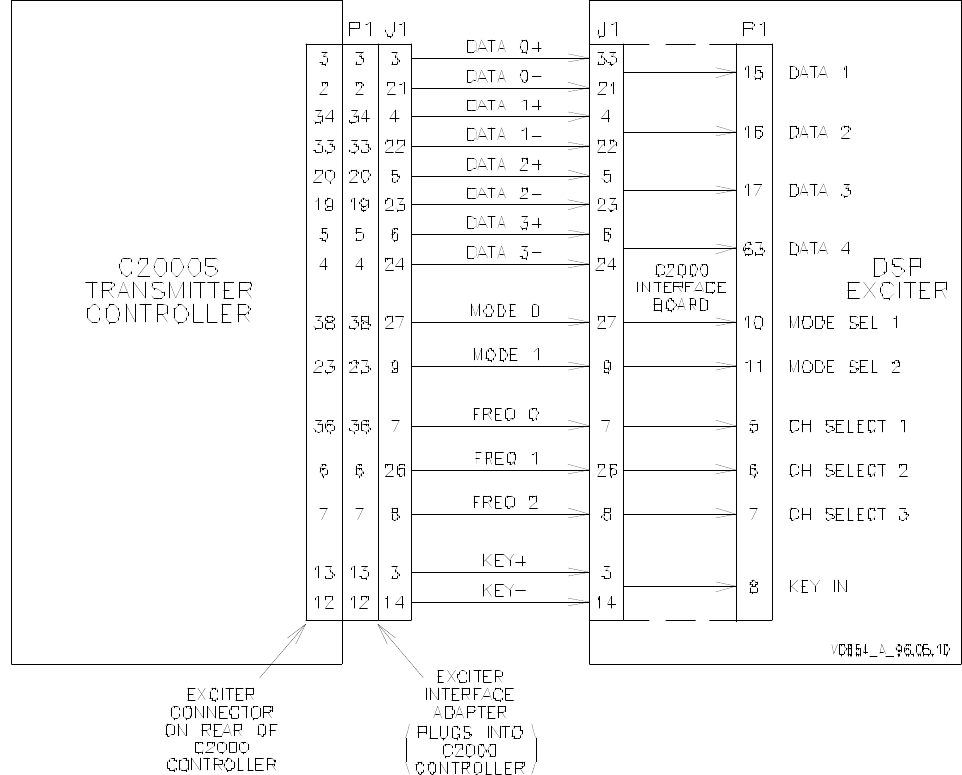
7.7 On-The-Fly Interface
Figure 7-1 On-The-Fly C2000 Control Lines to DSP Exciter
DSP Exciter Glenayre Document Number: 9110.00172
MAINTENANCE Issue 1, Rev. I: 01/15/97
Page: 7-6 Copyright © 1997 Glenayre Print Date: 02/19/97
Notes:
A C-2000 interface board in the DSP exciter must be used with on-the-fly software
All J1 pin connections shown on the above diagram are at the input to the C-2000 interface
board in the DSP exciter
Data 0 at the input of the C-2000 interface board controls Data 1 at its output
Data 1 at the input of the C-2000 interface board controls Data 2 at its output
Data 2 at the input of the C-2000 interface board controls Data 3 at its output
Data 3 at the input of the C-2000 interface board controls Data 4 at its output
Mode 0 at the input of the C-2000 interface board controls Mode sel 1 at its output
Mode 1 at the input of the C-2000 interface board controls Mode sel 2 at its output
Freq 0 at the input of the C-2000 interface board controls Ch select 1 at its output
Freq 1 at the input of the C-2000 interface board controls Ch select 2 at its output
Freq 2 at the input of the C-2000 interface board controls Ch select 3 at its output

Glenayre Document Number: 9110.00172 DSP Exciter
Issue 1, Rev. I: 01/15/97 CHECKOUT AND TROUBLESHOOTING
Print Date: 02/18/97 Copyright © 1997 Glenayre Page: 8-1
sec_8
8 CHECKOUT AND TROUBLESHOOTING
8.1 CHECKOUT
The DSP exciter has two functions; it produces on-frequency RF and has a microprocessor
to handle input from the PA and transmitter controller. Checkout involves verifying that RF
is produced and unkeying occurs during a fault condition.
8.2 TROUBLESHOOTING
The recommended troubleshooting level for the exciter is at the unit level. That is, if the
exciter fails to provide the transmitter system with a usable, modulated RF-drive signal and
all the exciter’s power, control, and signal inputs are normal, you should replace the exciter
with a spare.
DSP Exciter Glenayre Document Number: 9110.00172
CHECKOUT AND TROUBLESHOOTING Issue 1, Rev. I: 01/15/97
Page: 8-2 Copyright © 1997 Glenayre Print Date: 02/18/97

Glenayre Document Number: 9110.00172 DSP Exciter
Issue 1, Rev. I: 01/15/97 REMOVAL AND REINSTALLATION
Print Date: 02/19/97 Copyright © 1997 Glenayre Page: 9-1
sec_9
9 REMOVAL AND REINSTALLATION
Remove all input power from transmitter cabinet before performing these procedures.
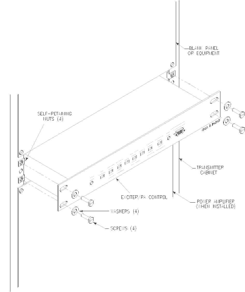
9.1 Exciter/PA Control Chassis
Refer to Figure 9-1, DSP Exciter Chassis Removal and Reinstallation, for a detailed
drawing.
Note
Memory PROMs in the replacement exciter should be the same as in the
original exciter unless the maintenance technician intends to modify
exciter characteristics. Also, parameters, such as channel frequencies,
may be stored in nonvolatile RAM. Ensure that the replacement exciter
is programmed correctly.
9.1.1 Removal Procedure
1. Support exciter while removing the four screws from the front panel that secure it to
the cabinet. Save screws for installation procedure.
2. Remove exciter from cabinet far enough to access back panel.
3. Disconnect connector J3 from connector P3 that is pigtailed off terminal board TB1
(dc power input).
4. If a controller interface I/O panel is mounted on exciter back panel, remove I/O panel;
leave all wires connected to I/O panel.
5. Tag all connectors attached to the exciter back panel.
6. Remove all connectors attached to the exciter back panel. Leave P3 connector/wiring
assembly connected to terminal board TB1 for now.
7. Remove exciter.
8. Tag wires connected to terminal board TB1 on P3 connector/wiring assembly.
9. Disconnect tagged wires from terminal board TB1. Save P3 connector/wiring assem-
bly for installation procedure.
Procedure is complete.
9.1.2 Reinstallation Procedure
Note
A wideband DSP exciter that is installed in a GL-T8500 or GL-T8600
transmitter must have one rack unit of space between it and the power
amplifier chassis.
DSP Exciter Glenayre Document Number: 9110.00172
REMOVAL AND REINSTALLATION Issue 1, Rev. I: 01/15/97
Page: 9-2 Copyright © 1997 Glenayre Print Date: 02/19/97
1. Before installing exciter, connect wires on P3 connector/wiring assembly to terminal
board TB1 on exciter back panel. P3 connector/wiring assembly is saved from remov-
al procedure.
2. Connect connectors on transmitter to exciter back panel.
3. If controller requires interface I/O panel, install external interface I/O board on exciter
back panel (see Paragraph 9.4).
4. Connect connector J3 to connector P3 that is pigtailed off of terminal board TB1.
5. Locate connector P3 that is pigtailed off of terminal board TB1. Disconnect connector
P3 from connector J3.
6. Slide exciter into cabinet and secure with four screws saved from removal procedure.
Procedure is complete. Perform setup, adjustment, or calibration procedures as required.
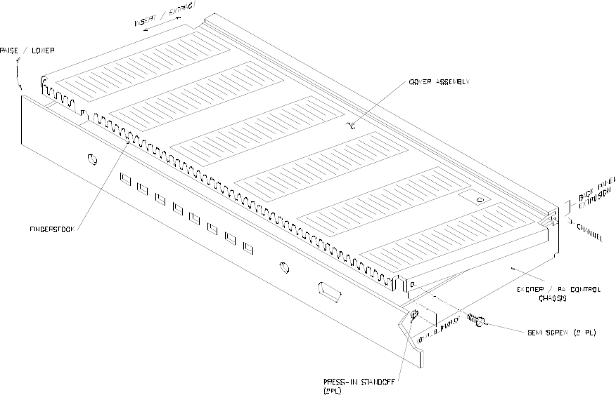
9.2 Exciter Cover
These procedures must be performed with the exciter removed from the transmitter cabinet.
Refer to Figure 9-2, DSP Exciter Cover Removal and Reinstallation throughout these
procedures.
9.2.1 Removal Procedure
1. Remove two sem screws from sides of exciter cover. Save sem screws for installation
procedure.
2. Raise front of cover and extract back of cover from channel in back panel extrusion.
3. Remove exciter cover.
Procedure is complete.
9.2.2 Reinstallation Procedure
1. Insert exciter cover into channel on exciter back panel extrusion.
2. Lower cover so that fingerstock is behind exciter front panel.
3. While pressing down slightly on exciter cover: install two sem screws saved from re-
moval procedure through sides of exciter cover.
Procedure is complete.
Glenayre Document Number: 9110.00172 DSP Exciter
Issue 1, Rev. I: 01/15/97 REMOVAL AND REINSTALLATION
Print Date: 02/19/97 Copyright © 1997 Glenayre Page: 9-3
sec_9
v0151.hgl
Figure 9-1 DSP Exciter Chassis Removal
and Reinstallation
DSP Exciter Glenayre Document Number: 9110.00172
REMOVAL AND REINSTALLATION Issue 1, Rev. I: 01/15/97
Page: 9-4 Copyright © 1997 Glenayre Print Date: 02/19/97
v0171.hgl
Figure 9-2 DSP Exciter Cover Removal
and Reinstallation

Glenayre Document Number: 9110.00172 DSP Exciter
Issue 1, Rev. I: 01/15/97 REMOVAL AND REINSTALLATION
Print Date: 02/19/97 Copyright © 1997 Glenayre Page: 9-5
sec_9
9.3 Exciter/Control Board
These procedures must be performed with the exciter removed from the transmitter cabinet,
and the exciter cover removed. Refer to Figure 9-3, DSP Exciter Control Board
Removal and Reinstallation, throughout these procedures.
9.3.1 Removal Procedure
Note
Save all hardware for installation procedure.
1. Remove controller interface board (see Table Paragraph 9.4 ).
2. Remove VCO/RF amplifier board (see Table Paragraph 9.5 ).
3. Remove three kep nuts and three screws from regulators U1, U2, and U58.
4. Remove shoulder washer from regulator U58.
5. Remove two jam nuts and two lock washers from connectors J7 and J8.
6. Remove two jack socket screws attached to connector J6 through back panel.
7. Remove four sem screws from back panel and remove back panel from exciter chas-
sis. Some exciters use three sem screws and one standoff.
8. Remove insulator between back panel and regulator U58.
9. Remove two jack socket screws attached to connector J3 through front panel.
10.Remove two studded standoffs through exciter/control board.
11.Remove nine sem screws that attach exciter/control board to exciter chassis, and re-
move exciter/control board.
Procedure is complete.
9.3.2 Reinstallation Procedure
Note
Use hardware saved from installation procedure.
1. Position exciter/control board onto exciter chassis and secure with nine sem screws.
2. Install two studded standoffs through exciter/control board.
3. Apply Vibra Tite or similar nonpermanent self-locking liquid adhesive to threads of
the two jack socket screws to be used for connector J3. Apply only to top 1/4 inch of
thread on each jack socket screw.
4. Install two jack socket screws into connector J3 through front panel.
5. Apply thermal compound as follows: between regulator U1 and back panel, between
regulator U2 and back panel, between regulator U58 and insulator, and between insu-
lator and back panel.
6. Install insulator between regulator U58 and back panel.
DSP Exciter Glenayre Document Number: 9110.00172
REMOVAL AND REINSTALLATION Issue 1, Rev. I: 01/15/97
Page: 9-6 Copyright © 1997 Glenayre Print Date: 02/19/97
7. Position back panel on exciter chassis and secure with four sem screws. Some excit-
ers use three sem screws and one standoff in the bottom right corner.
8. Apply Vibra Tite or similar nonpermanent self-locking liquid adhesive to threads of
the two jack socket screws to be used for connector J6. Apply only to top 1/4 inch of
thread on each jack socket screw.
9. Install two jack socket screws into connector J6 through back panel.
10.Install two lock washers and two jam nuts over connectors J7 and J8.
11.Install shoulder washer into regulator U58.
12.Install three kep nuts and three screws through regulators U1, U2, and U58.
13.Install VCO/RF amplifier board (see Table Paragraph 9.5 ).
14.Install controller interface board (see Table Paragraph 9.4 ).
Procedure is complete. After exciter is installed in transmitter cabinet: perform setup
procedure if necessary (refer to the system and menu manuals).
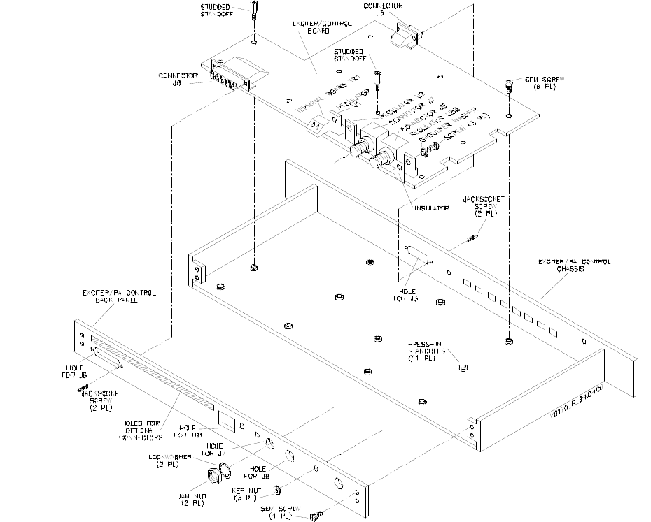
Glenayre Document Number: 9110.00172 DSP Exciter
Issue 1, Rev. I: 01/15/97 REMOVAL AND REINSTALLATION
Print Date: 02/19/97 Copyright © 1997 Glenayre Page: 9-7
sec_9
v0170.hgl
Figure 9-3 DSP Exciter Control Board Removal and Reinstallation
DSP Exciter Glenayre Document Number: 9110.00172
REMOVAL AND REINSTALLATION Issue 1, Rev. I: 01/15/97
Page: 9-8 Copyright © 1997 Glenayre Print Date: 02/19/97
9.4 Interface Board
These procedures must be performed with the exciter removed from the transmitter cabinet
(see Paragraph 9.1), and the exciter cover removed (see Paragraph 9.2). Refer to
Figure 9-4, DSP Exciter External Interface I/O Board Removal and Reinstallation,
throughout the following procedures.
9.4.1 Removal Procedure
1. Remove jack socket screws (2 or 6) securing connector J4 (J1 and J2 not always used)
to the rear panel of the exciter. Save jack socket screws for installation procedure.
2. Remove two sem screws securing interface board to standoffs. Save sem screws for
installation procedure.
3. Grasp interface board at the center of connector P1. Pull up on board with a firm ver-
tical motion to disengage connector P1 from connector J1 on the exciter/control
board.
4. Remove interface board.
Procedure is complete.
9.4.2 Reinstallation Procedure
1. Position interface board into place by inserting connector J4 (and J1 and J2 if used)
through openings in exciter rear panel.
2. Carefully align connector P1 on interface board with connector J1 on exciter/control
board and engage.
3. Secure interface board to standoffs with two sem screws saved from removal proce-
dure.
4. Apply Vibra Tite or similar nonpermanent self-locking liquid adhesive to threads of
the six jack socket screws saved from removal procedure. Apply only to top 1/4 inch
of thread on each jack socket screw.
5. Screw the six jack socket screws through holes on exciter rear panel at either sides of
connectors J1, J4, and J2.
Procedure is complete. After exciter is installed into transmitter cabinet, perform audio
input adjustment procedure (see Section 7).
9.5 VCO/RF Amplifier Board
These procedures must be performed with the exciter removed from the transmitter cabinet
(see Paragraph 9.1), and the exciter cover removed (see Paragraph 9.2). Refer to
Figure 9-5, DSP Exciter Interface Board Removal and Reinstallation, throughout
these procedures.

Glenayre Document Number: 9110.00172 DSP Exciter
Issue 1, Rev. I: 01/15/97 REMOVAL AND REINSTALLATION
Print Date: 02/19/97 Copyright © 1997 Glenayre Page: 9-9
sec_9
9.5.1 Removal Procedure
1. Remove jam nut and lock washer from connector J3 on rear of exciter. Save jam nut
and lock washer for installation procedure.
2. Remove five sem screws securing VCO/RF amplifier board to standoffs on exciter.
Save sem screws for installation procedure.
3. Grasp VCO/RF amplifier board near connector P4. Pull up on board with a short ver-
tical motion to disengage connectors P4/P9/P10 from connectors J4/J9/J10 on exciter/
control board.
4. Remove VCO/RF amplifier board.
Procedure is complete.
9.5.2 Reinstallation Procedure
1. Before installing VCO/RF amplifier board, verify that RF band includes desired
transmitter operating frequencies (refer to Section 10).
2. Position VCO/RF amplifier board into place by inserting connector J3 through hole in
rear of exciter.
3. Carefully align connectors P4/P9/P10 on VCO/RF amplifier board with connectors
J4/J9/J10 on exciter/control board and engage.
4. Secure VCO/RF amplifier board to standoffs on exciter using five sem screws saved
from removal procedure.
5. Install lockwasher and jam nut to connector J3 on rear of exciter using lockwasher
and jam nut saved from removal procedure.
Procedure is complete. After exciter is installed into transmitter cabinet, perform VCO2
adjustment procedure in Section 7.
DSP Exciter Glenayre Document Number: 9110.00172
REMOVAL AND REINSTALLATION Issue 1, Rev. I: 01/15/97
Page: 9-10 Copyright © 1997 Glenayre Print Date: 02/19/97
v0341.hgl
Figure 9-4 DSP Exciter External Interface I/O Board
Removal and Reinstallation
Glenayre Document Number: 9110.00172 DSP Exciter
Issue 1, Rev. I: 01/15/97 REMOVAL AND REINSTALLATION
Print Date: 02/19/97 Copyright © 1997 Glenayre Page: 9-11
sec_9
v0342.hgl
Figure 9-5 DSP Exciter Interface Board Removal and Reinstallation
DSP Exciter Glenayre Document Number: 9110.00172
REMOVAL AND REINSTALLATION Issue 1, Rev. I: 01/15/97
Page: 9-12 Copyright © 1997 Glenayre Print Date: 02/19/97

Glenayre Document Number: 9110.00172 DSP Exciter
Issue 1, Rev. I: 01/15/97 OPTIONS
Print Date: 02/19/97 Copyright © 1997 Glenayre Page: 10-1
dspsec10
10 OPTIONS
10.1 Exciter/PA Control with QT-1000 Interface
The controller interface is the portion of exciter circuitry that connects the transmitter
controller to the exciter. The controller interface dictates what kind of transmitter controller
may operate the transmitter. The transmitter can be operated through one of several control-
lers depending on the interface circuitry installed with the exciter.
Two boards form this interface, the internal QT-1000 interface board and the external
interface I/O board.
Control commands from the transmitter controller are connected through the interface
circuit. This circuit supplies remote control to the microcontroller unit (MCU) control
circuit. The VT-100 VDT supplies local control. The MCU control circuit generates all
control signals for the other circuits, and monitors their status. The MCU control circuit
reports status back to the VT-100 VDT and the interface circuit, which supplies the status
to the transmitter controller.
10.1.1 Reference Source
The ten-MHz reference signal is provided by the controller via J8 on the exciter/control
board.
10.1.2 Controller Interface Connector Functions
Refer to Figure 10-1, Table 10-1, and Table 10-2 for a pin-by-pin description of signal
functions. The controller interfaces with the transmitter through connectors J1, J2, and J5
and terminal board TB2 at the exciter back panel. J5 on the external I/O board connects to
a standard RL-XX3 receiver, if installed. If a standard receiver is not installed, TB2 on the
external I/O board connects to any generic receiver. TB2 also makes connections to
optional configurable QT-1000 alarm inputs and switching outputs. J1 on the internal
interface board connects directly to TXC connector J1, and interfaces all signals except
alarms. Alarm signals, consisting of transmitter alarm, fault, and status signals, are supplied
directly to the QT-1000 controller connector J2 though J2 on the internal interface board.
10.1.3 QT-1000 Interface Conversion Functions
Many of the signals exchanged between the controller and the exciter originate with a
format, voltage, or requirement incompatible with their destination. The QT-1000 interface
performs any signal conversions necessary to provide compatibility between the controller
and the exciter. The following text describes any signal conversions made by the controller
interface.
DSP Exciter Glenayre Document Number: 9110.00172
OPTIONS Issue 1, Rev. I: 01/15/97
Page: 10-2 Copyright © 1997 Glenayre Print Date: 02/19/97
10.1.3.1 Analog-Mode A/D Conversion
The exciter DSP modulator circuit reads synchronized serial data for its analog mode input
signal, but the QT-1000 controller provides an analog signal. The controller interface
converts the analog to the appropriate data form for the DSP. The analog (FLAT AUDIO+,-
) terminates across a balanced input circuit that also provides a level adjustment. The
adjustment, when properly set by the AUDIO INPUT ADJUST pot through the exciter
cover, provides analog to an A/D converter at the optimum zero-dBm level. The A/D
converts the analog into serial data, which is applied to the DSP through a synchronous data
link. A synchronous data link is characterized by an exchange of pulse streams for timing
purposes. The A/D converter is clocked by a pulse generator circuit driven by the ten-MHz
reference circuit.
10.1.3.2 FSK-Data-Bit Strapping
The exciter DSP modulator circuit can read up to four bits for its digital FSK mode input
signal, but the controller provides two active bits 1 and 2 (DATA1, DATA2). This allows
transmitter operation in the two-level or four-level mode.
10.1.3.3 Channel-Select-Bit Strapping
The exciter MCU control circuit reads three bits to determine the remotely selected
channel, but the QT-1000 controller provides only bits 1 and 2 (CH SEL 1,2). As a result,
the QT-1000 controller can command only four channels. The controller interface keeps bit
3 open (high). Table 10-2 defines the transmitter operating channel resulting from the
channel select inputs.
10.1.3.4 Mode-Select-Bit Strapping
The exciter MCU control circuit reads two bits to determine the remotely selected mode,
but the QT-1000 controller provides only bit 1 (MODE CONTROL). As a result, the QT-
1000 controller can command only two modes. The controller interface straps bit 2 to
ground (low). Table 10-3 defines the transmitter operating mode resulting from the model
select input.
10.1.3.5 Power Sample D/A Conversion
The QT-1000 controller reads two 0-to-2.5-volt voltages for its forward and reflected
power sample inputs, but these power values are stored as data in the exciter MCU control
circuit. The controller interface converts the data to voltages of the appropriate range for
the QT-1000 controller. Data from the MCU representing the forward and reflected powers
is written into a dual D/A converter. The D/A converts the data into two proportional dc
voltages ranging from 0 volt to 2.5 volts (FWD PWR SAMPLE, REF PWR SAMPLE),
which are applied to the QT-1000 controller. Control logic gates ensure that data is written
to the proper half of the D/A converter.
Glenayre Document Number: 9110.00172 DSP Exciter
Issue 1, Rev. I: 01/15/97 OPTIONS
Print Date: 02/19/97 Copyright © 1997 Glenayre Page: 10-3
dspsec10
Table 10-1 Interface Board Connector J4 (QT-1000)
J4-X signal/description J4-X signal/description
1 FWD PWR SAMPLE, input from PA 14 AUDIO INPUT +, input from receiver or tx con-
troller
2 AUDIO INPUT -, common 15 REF PWR SAMPLE, input from PA
3 TX GND 16 TONE DECODER OUTPUT, logic output to tx
controller
4 KEY IN, input from tx controller 17 DATA 1, digital data input from tx controller
5 DATA 2, digital data input from tx controller 18 DATA 3, digital data input from tx controller
6 CH SELECT 3, digital command input from tx con-
troller
19 MODE SELECT 1, digital command input from
tx controller
7 MODE SELECT 2, digital command input from tx
controller
20 LOW POWER MODE, logic input from PA
8 FAULT ALARM, digital output to tx controller 21 VSWR ALARM, logic output to tx controller
9 DATA4/CLK, input from tx controller 22 CH SELECT 1, logic input from tx controller
10 CH SELECT 2, logic input from tx controller 23 MOD IND, logic output to tx controller
11 LOW POWER ALARM, output to tx controller 24 TEMP ALARM, logic output to tx controller
12 SHUTDOWN ALARM, output to tx controller 25 RF INPUT ALARM, logic output to tx controller
13 not used -- --
DSP Exciter Glenayre Document Number: 9110.00172
OPTIONS Issue 1, Rev. I: 01/15/97
Page: 10-4 Copyright © 1997 Glenayre Print Date: 02/19/97
Note
Not all transmitters can do all the modes.
Table 10-2 Receiver Connector J5 Pin Functions
(QT-1000 with external I/O board)
J5-X function J5-X function
1 no connection 9 no connection
2 standard receiver audio input for interface,
2 Vp-p, nominal
10 no connection
3 no connection 11 return for standard receiver audio
4 no connection 12 standard receiver RSSI input for interface,
0.5-6.0 Vdc
5 no connection 13 no connection
6 standard receiver ground for interface 14 standard receiver-fault alarm input for inter-
face, LO=OK
7 no connection 15 no connection
8 standard receiver squelch output for inter-
face, HI=unsquelched
Table 10-3 Remote Select Input vs. Channel (QT-1000)
ch sel 1 J1-5 ch sel 2 J1-24 ch sel 3 selected
channel
command open (HI) command open (HI) open (HI) 1
command ground (LO) command open (HI) open (HI) 2
command open (HI) command ground (LO) open (HI) 3
command ground (LO) command ground (LO) open (HI) 4
Table 10-4 Remote Select Input vs. Mode (QT-1000)
mode sel 1 J1-25 mode sel 2 J2-1 selected mode
command ground (LO) ground (LO) analog
command open (HI) ground (LO) 2-level
command open (HI) command open (HI) 4-level

Glenayre Document Number: 9110.00172 DSP Exciter
Issue 1, Rev. I: 01/15/97 OPTIONS
Print Date: 02/19/97 Copyright © 1997 Glenayre Page: 10-5
dspsec10
10.2 Exciter/PA Control with Standard Interface
The following major paragraphs describe the operation of the major items within the
standard interface. Detailed figures are referenced, as required.
The controller interface is the portion of exciter circuitry that connects the transmitter
controller to the exciter. The controller interface dictates what kind of transmitter controller
may operate the transmitter. The transmitter can be operated through one of several control-
lers depending on the interface circuitry installed at the exciter. The remainder of section
10.2 describes standard controller interface circuitry.
Two boards form this interface, the internal standard interface board and the external
exciter standard interface I/O board.
Control commands from the transmitter controller are connected through the interface
circuit. This circuit supplies remote control to the microcontroller unit (MCU) control
circuit. The VT-100 VDT supplies local control. The MCU control circuit generates all
control signals for the other circuits, and monitors their status. The MCU control circuit
reports status back to the VT-100 VDT and the interface circuit, which supplies the status
to the transmitter controller.
10.2.1 Reference Source
The ten-MHz reference signal is provided by the controller via J8 on the exciter/control
board. All other inputs and outputs, except for RF output, are routed through the standard
interface board.
10.2.2 Controller Interface Connector Functions
Refer to Table 10-1, Interface Board Connector J4 (QT-1000), for a pin-by-pin descrip-
tion of signal functions. The controller interfaces with the transmitter through connector J4
and terminal board TB2 at the exciter back panel. TB2 also makes connections to optional
configurable alarm inputs and switching outputs.
10.2.3 Standard Interface Conversion Functions
Many of the signals exchanged between the controller and the exciter originate with a
format, voltage, or requirement incompatible with their destination. The standard interface
performs any signal conversions necessary to provide compatibility between the controller
and the exciter. The following text describes any signal conversions made by the controller
interface.
10.2.3.1 Analog-Mode A/D Conversion
The exciter DSP modulator circuit reads synchronized serial data for its analog mode input
signal, but the transmitter controller provides an analog signal. The controller interface
converts the analog to the appropriate data form for the DSP. The analog (FLAT AUDIO
+,-) terminates across a balanced input circuit that also provides a level adjustment. The
adjustment, when properly set by the AUDIO INPUT ADJUST pot through the exciter
cover, provides analog to an A/D converter at the optimum zero-dBm level. The A/D
DSP Exciter Glenayre Document Number: 9110.00172
OPTIONS Issue 1, Rev. I: 01/15/97
Page: 10-6 Copyright © 1997 Glenayre Print Date: 02/19/97
converts the analog into serial data, which is applied to the DSP through a synchronous data
link. A synchronous data link is characterized by an exchange of pulse streams for timing
purposes. The A/D converter is clocked by a pulse generator circuit driven by the exciter’s
ten-MHz reference circuit.
10.2.3.2 FSK-Data-Bit Strapping
The exciter DSP modulator circuit can read up to four bits for its digital FSK mode input
signal, but the controller provides two active bits 1 and 2 (DATA1, DATA2). This allows
transmitter operation in the two-level or four-level mode.
10.2.3.3 Channel-Select-Bit Strapping
The exciter MCU control circuit reads three bits to determine the remotely selected
channel, and the transmitter controller provides bits 1, 2, and 3 (CH SEL 1,2,3). As a result,
the transmitter controller can command all eight of the possible channels. Table 10-3,
Remote Select Input vs. Channel (QT-1000), defines the transmitter operating channel
resulting from the channel select inputs.
10.2.3.4 Mode-Select-Bit Strapping
The exciter MCU control circuit reads two bits to determine the remotely selected mode,
but the transmitter controller provides only bit 1 (MODE CONTROL). As a result, the
transmitter controller can command three of the transmitter’s four possible modes.
Table 10-4, Remote Select Input vs. Mode (QT-1000), defines the transmitter operating
mode resulting from the model select input.
10.2.3.5 Power Sample D/A Conversion
The transmitter controller reads two 0-to-2.5-volt voltages for its forward and reflected
power sample inputs, but these power values are stored as data within the exciter’s MCU
control circuit. The controller interface converts the data to voltages of the appropriate
range for the transmitter controller. Data from the MCU representing the forward and
reflected powers is written into a dual D/A converter. The D/A converts the data into two
proportional dc voltages ranging from 0 volt to 2.5 volts (FWD PWR SAMPLE, REF PWR
SAMPLE), which are applied to the transmitter controller. Control logic gates ensure that
data is written to the proper half of the D/A converter.
Glenayre Document Number: 9110.00172 DSP Exciter
Issue 1, Rev. I: 01/15/97 OPTIONS
Print Date: 02/19/97 Copyright © 1997 Glenayre Page: 10-7
dspsec10
Table 10-5 Interface Board Connector J4 (Standard)
J4-X signal/description J4-X signal/description
1 FWD PWR SAMPLE, input from PA 14 AUDIO INPUT -, input from receiver or tx controller
2 AUDIO INPUT +, common 15 REF PWR SAMPLE, input from PA
3 TX GND 16 TONE DECODER OUTPUT, logic output to tx con-
troller
4 KEY IN, input from tx controller 17 DATA 1, digital data input from tx controller
5 DATA 2, digital data input from tx controller 18 DATA 3, digital data input from tx controller
6 CH SELECT 3, digital command input from tx
controller
19 MODE SELECT 1, digital command input from tx
controller
7 MODE SELECT 2, digital command input
from tx controller
20 LOW POWER MODE, logic input from PA
8 FAULT ALARM, digital output to tx controller 21 VSWR ALARM, logic output to tx controller
9 DATA4/CLK, input from tx controller 22 CH SELECT 1, logic input from tx controller
10 CH SELECT 2, logic input from tx controller 23 MOD IND, logic output to tx controller
11 LOW POWER ALARM, output to tx controller 24 TEMP ALARM, logic output to tx controller
12 SHUTDOWN ALARM, output to tx controller 25 RF INPUT ALARM, logic output to tx controller
13 not used -- --
Table 10-6 Remote Select Input vs. Channel (standard)
ch sel 1 J1-5 ch sel 2 J1-24 ch sel 3 selected
channel
command open (HI) command open (HI) open (HI) 1
command ground (LO) command open (HI) open (HI) 2
command open (HI) command ground (LO) open (HI) 3
command ground (LO) command ground (LO) open (HI) 4
command open (HI) command open (HI) command ground (LO) 5
command ground (LO) command open (HI) command ground (LO) 6
command open (HI) command ground (LO) command ground (LO) 7
command ground (LO) command ground (LO) command ground (LO) 8

DSP Exciter Glenayre Document Number: 9110.00172
OPTIONS Issue 1, Rev. I: 01/15/97
Page: 10-8 Copyright © 1997 Glenayre Print Date: 02/19/97
Note
Not all transmitters can do all the modes.
10.3 Exciter/PA Control with I20 Interface
The following major paragraphs describe the operation of the major items within the I20
interface. Detailed figures are referenced, as required.
The controller interface is the portion of exciter circuitry that connects the transmitter
controller to the exciter. The controller interface dictates what kind of transmitter controller
may operate the transmitter. The transmitter can be operated through one of several control-
lers depending on the interface circuitry installed at the exciter. The remainder of section
10.3 describes I20 controller interface circuitry.
Two boards form this interface, the internal I20 interface board and the external I20
interface I/O board.
Control commands from the transmitter controller are connected through the interface
circuit. This circuit supplies remote control to the microcontroller unit (MCU) control
circuit. The VT-100 VDT supplies local control. The MCU control circuit generates all
control signals for the other circuits, and monitors their status. The MCU control circuit
reports status back to the VT-100 VDT and the interface circuit, which supplies the status
to the transmitter controller.
10.3.1 Reference Source
The ten-MHz reference signal is provided by the controller via J8 on the exciter/control
board.
10.3.2 Controller Interface Connector Functions
Refer to Table 10-8 and Table 10-9 for a pin-by-pin description of signal functions. The
exciter interfaces with the transmitter through connector J2 and the controller through J1.
Table 10-7 Remote Select Input vs. Mode (standard)
mode sel 1 J1-25 mode sel 2 J2-1 selected mode
command ground (LO) ground (LO) analog
command open (HI) ground (LO) 2-level
command open (HI) command open (HI) 4-level

Glenayre Document Number: 9110.00172 DSP Exciter
Issue 1, Rev. I: 01/15/97 OPTIONS
Print Date: 02/19/97 Copyright © 1997 Glenayre Page: 10-9
dspsec10
10.3.3 I20 Interface Conversion Functions
Many of the signals exchanged between the controller and the exciter originate with a
format, voltage, or requirement incompatible with their destination. The I20 interface
performs any signal conversions necessary to provide compatibility between the controller
and the exciter. The following text describes any signal conversions made by the controller
interface.
10.3.3.1 Analog-Mode A/D Conversion
The exciter DSP modulator circuit reads synchronized serial data for its analog mode input
signal, but the transmitter controller provides an analog signal. The controller interface
converts the analog to the appropriate data form for the DSP. The analog (FLAT AUDIO
+,-) terminates across a balanced input circuit that also provides a level adjustment. The
adjustment, when properly set by the AUDIO INPUT ADJUST pot through the exciter
cover, provides analog to an A/D converter at the optimum zero-dBm level. The A/D
converts the analog into serial data, which is applied to the DSP through a synchronous data
link. A synchronous data link is characterized by an exchange of pulse streams for timing
purposes. The A/D converter is clocked by a pulse generator circuit driven by the ten-MHz
reference circuit.
10.3.3.2 FSK-Data-Bit Strapping
The exciter DSP modulator circuit can read up to four bits for its digital FSK mode input
signal, but the controller provides two active bits 1 and 2 (DATA1, DATA2). This allows
transmitter operation in the two-level or four-level mode.
10.3.3.3 Channel-Select-Bit Strapping
The exciter MCU control circuit reads three bits to determine the remotely selected
channel, and the transmitter controller provides bits 1, 2, and 3 (CH SEL 1,2,3). As a result,
the transmitter controller can command all eight of the possible channels. Table 10-3
defines the transmitter operating channel resulting from the channel select inputs.
10.3.3.4 Mode-Select-Bit Strapping
The exciter MCU control circuit reads two bits to determine the remotely selected mode,
and the transmitter controller provides two bits (MODE SELECT 1, MODE SELECT 2).
As a result, the transmitter controller can command three of the transmitter’s four possible
modes. Table 10-4 defines the transmitter operating mode resulting from the model select
input.
10.3.3.5 Power Sample D/A Conversion
The transmitter controller reads two 0-to-2.5-volt voltages for its forward and reflected
power sample inputs, but these power values are stored as data within the exciter’s MCU
control circuit. The controller interface converts the data to voltages of the appropriate
range for the transmitter controller. Data from the MCU representing the forward and
reflected powers is written into a dual D/A converter. The D/A converts the data into two

DSP Exciter Glenayre Document Number: 9110.00172
OPTIONS Issue 1, Rev. I: 01/15/97
Page: 10-10 Copyright © 1997 Glenayre Print Date: 02/19/97
proportional dc voltages ranging from 0 volt to 2.5 volts (FWD PWR SAMPLE, REF PWR
SAMPLE), which are applied to the transmitter controller. Control logic gates ensure that
data is written to the proper half of the D/A converter.
Table 10-8 Interface Board Connector J1
J1-X signal/description J1-X signal/description
1 CHASSIS 20 CLOCK-
2 CLOCK+ 21 DATA0-
3 DATA0+ 22 DATA1-
4 DATA1+ 23 DATA2-
5 DATA2+ 24 DATA3-
6DATA3+ 25 GND
7 FREQ0 26 FREQ1
8 FREQ2 27 MODE 0
9 MODE 1 28 MODE/AUX
10 ANALOG+ 29 ANALOG-
11 GND 30 GND
12 RxD- 31 RxD+
13 TxD- 32 TxD+
14 KEY- 33 KEY+
15 DIG OUT 6 34 DIG OUT 7
16 DIG OUT 4 35 DIG OUT 5
17 DIG OUT 2 36 DIG OUT 3
18 DIG OUT 0 37 DIG OUT 1
19 _RESET
Glenayre Document Number: 9110.00172 DSP Exciter
Issue 1, Rev. I: 01/15/97 OPTIONS
Print Date: 02/19/97 Copyright © 1997 Glenayre Page: 10-11
dspsec10
Table 10-9 Interface Board Connector J2
J2-X signal/description J2-X signal/description
1 not used 8 GND
2TxD+ 9 TxD-
3 KEY+ 10 KEY-
4 RxD+ 11 RxD-
5 DATA0+ 12 DATA0-
6 CLOCK+ 13 CLOCK-
7 DATA1+ 14 DATA1-
Table 10-10 Remote Select Input vs. Channel (I20)
ch sel 1 J1 ch sel 2 J1 ch sel 3 selected channel
command open (HI) command open (HI) open (HI) 1
command ground (LO) command open (HI) open (HI) 2
command open (HI) command ground (LO) open (HI) 3
command ground (LO) command ground (LO) open (HI) 4
command open (HI) command open (HI) command
ground (LO)
5
command ground (LO) command open (HI) command
ground (LO)
6
command open (HI) command ground (LO) command
ground (LO)
7
command ground (LO) command ground (LO) command
ground (LO)
8
Table 10-11 Remote Select Input vs. Mode (I20)
mode sel 1 J1-25 mode sel 2 J2-1 selected mode
command ground (LO) ground (LO) analog
command open (HI) ground (LO) 2-level
command open (HI) command open (HI) 4-level
DSP Exciter Glenayre Document Number: 9110.00172
OPTIONS Issue 1, Rev. I: 01/15/97
Page: 10-12 Copyright © 1997 Glenayre Print Date: 02/19/97