HARRIS TR-307-A Land Mobile Basestation Transceiver User Manual Manual
HARRIS CORPORATION Land Mobile Basestation Transceiver Manual
UserManual.wiki
>
HARRIS
>
TR 307 A User Manual
Manual
Navigation menu
Upload a User Manual
Namespaces
Wiki Guide
HTML
PDF
Info
Views
User Manual
Discussion / Help
Navigation

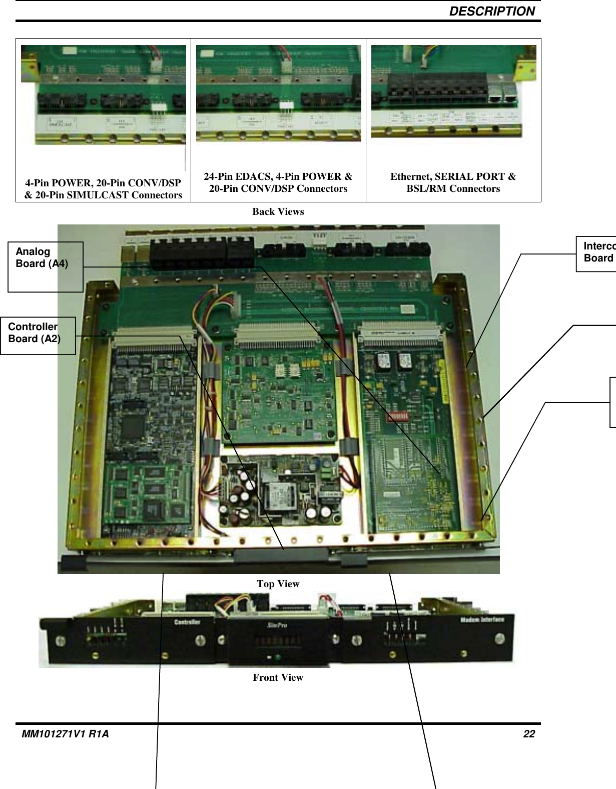
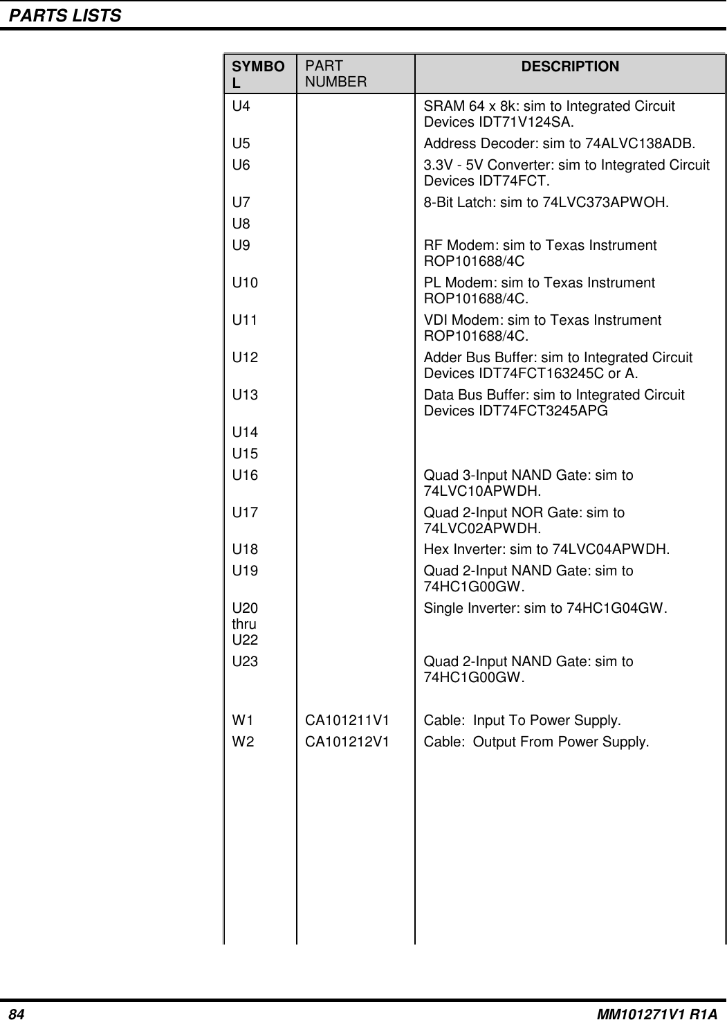
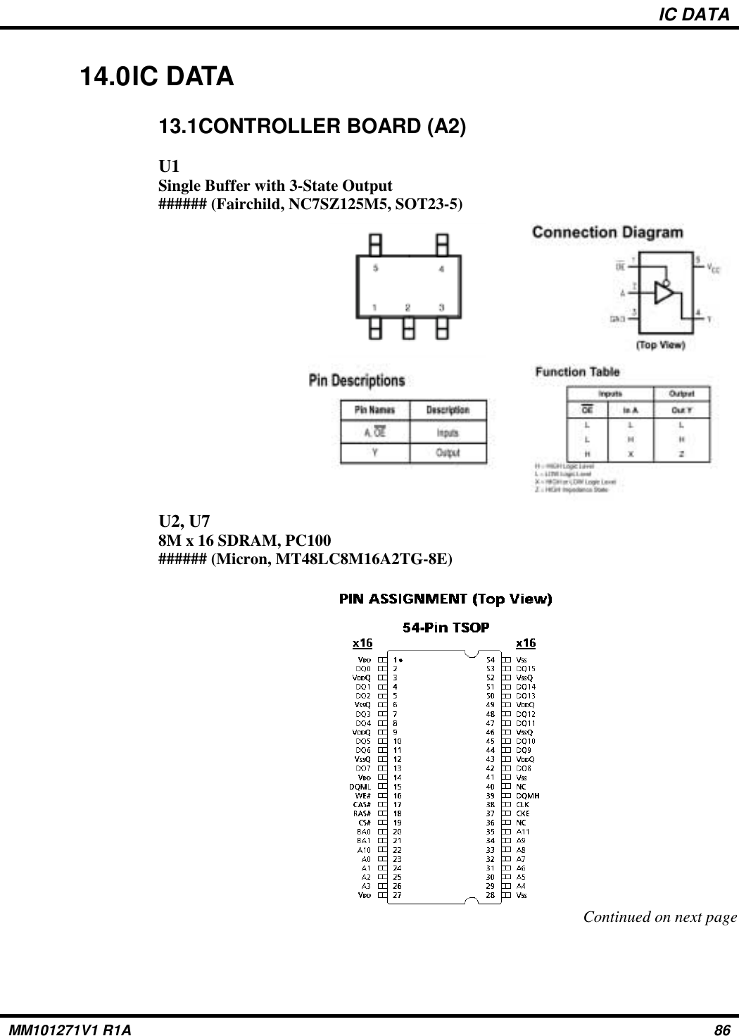
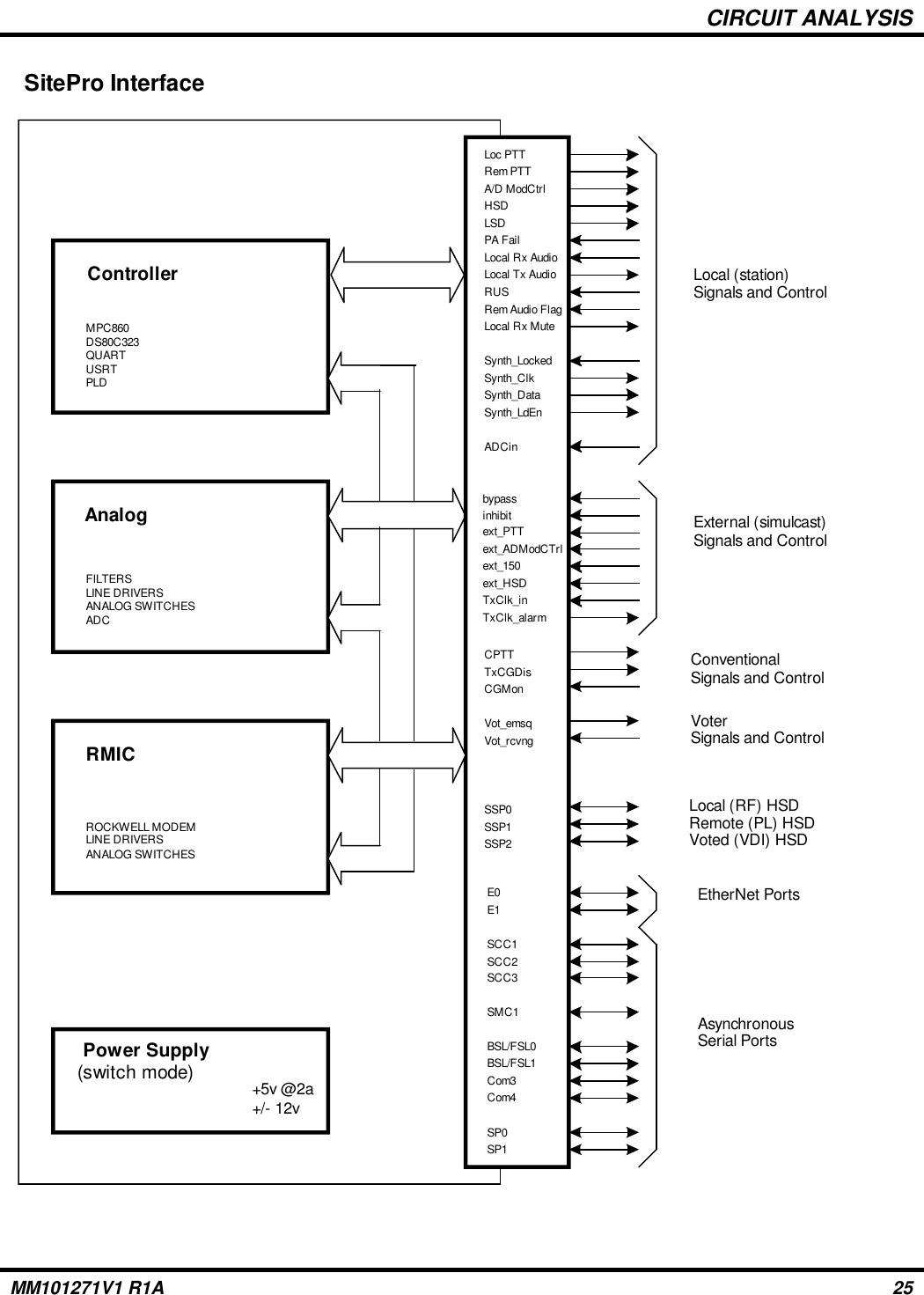
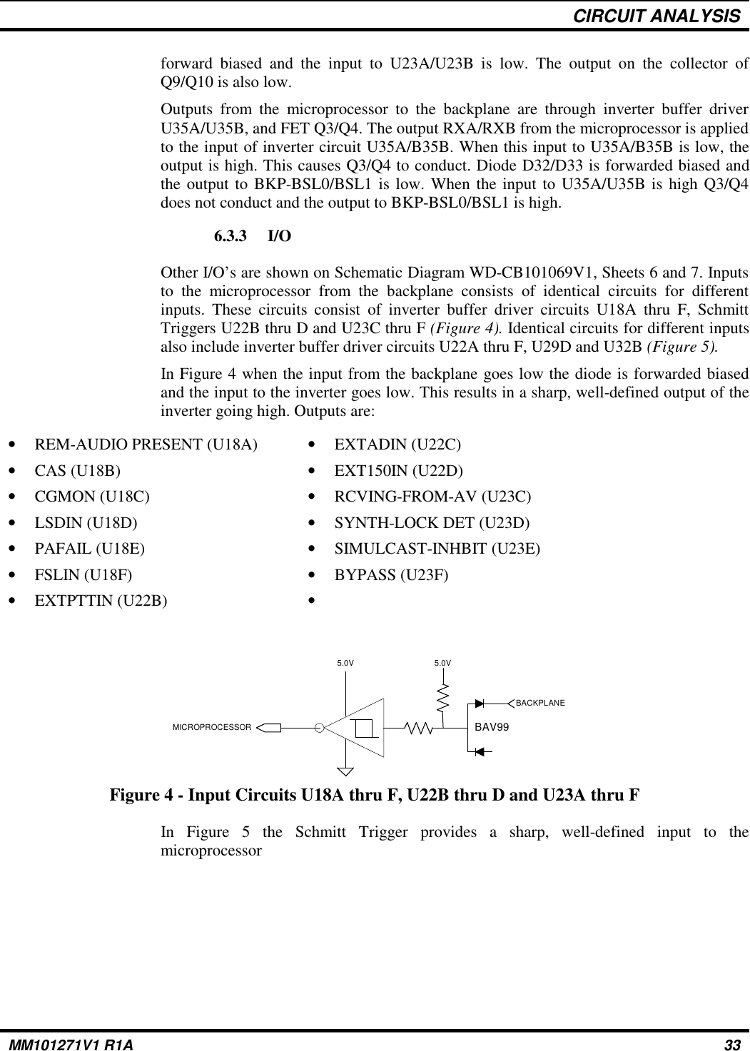
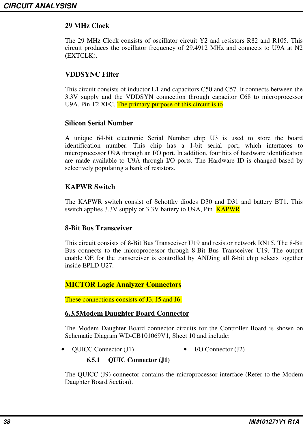
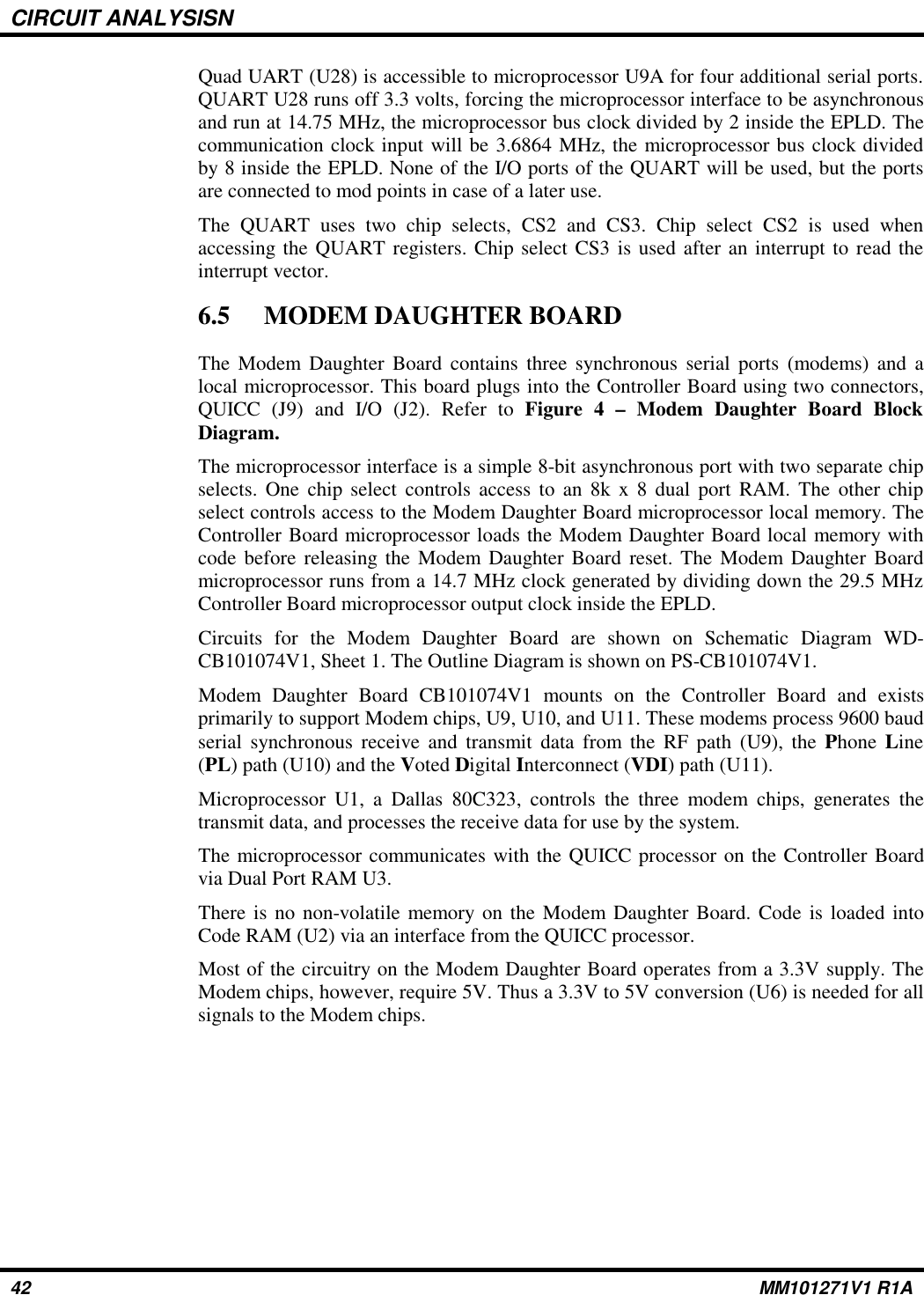
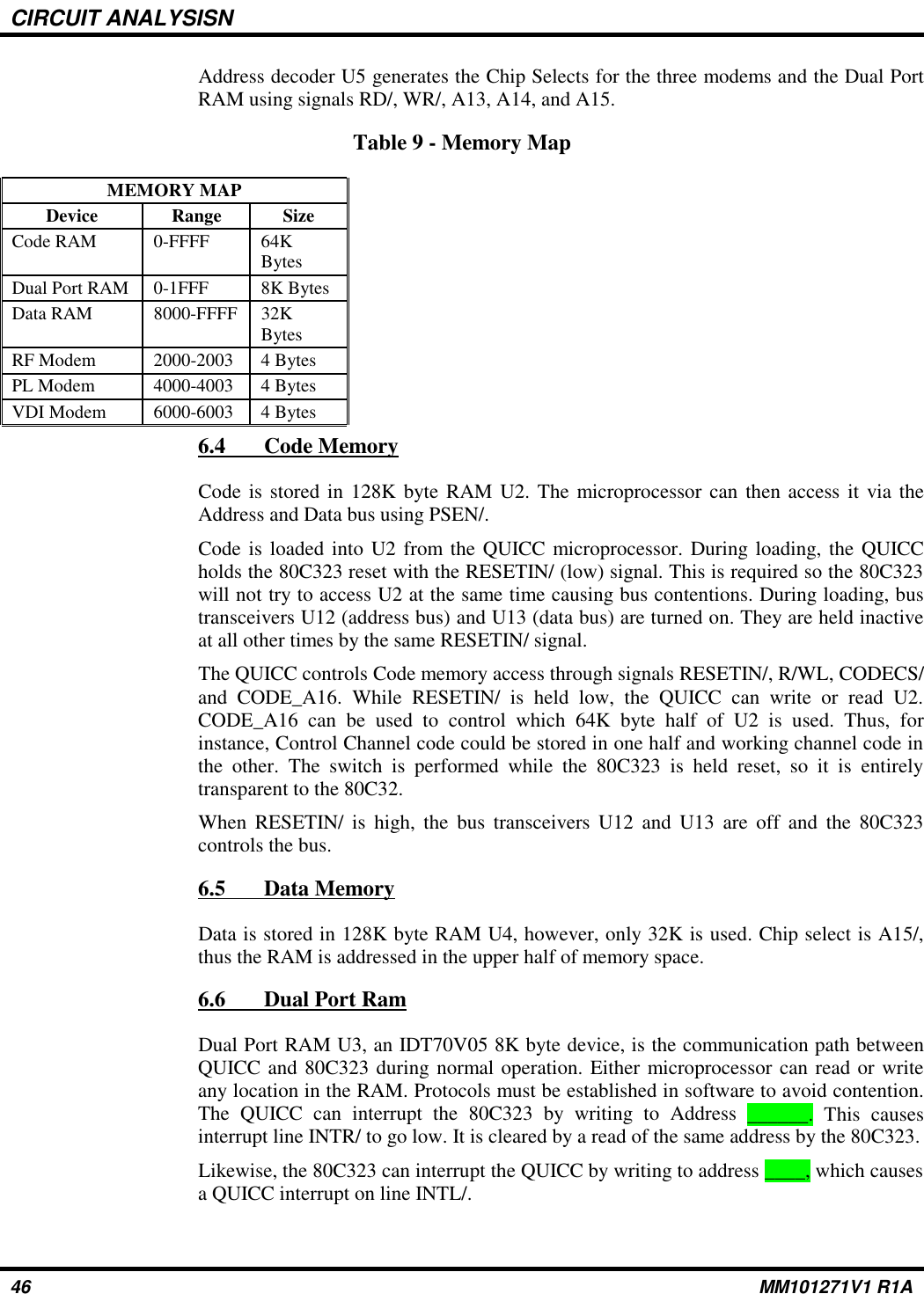
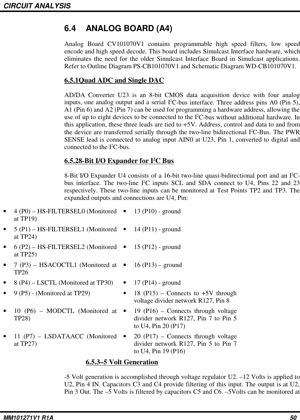
![CIRCUIT ANALYSIS6.0 CIRCUIT ANALYSISThe Theory of operation of each circuit board/card and module used in SiteProController Shelf Assembly EA101209V1 is described in the following paragraphs.Refer to the Block Diagram in Figure 2 and Outline and Schematic Diagrams as listed inthe TABLE OF CONTENTS.The SitePro Controller is a Base Station Controller with redundant communicationlinks [Backup Serial Links (BSL’s)]. The BSL’s provide for inter-channelcommunication with two 10Mbit Ethernet Ports. The BSL’s provide trunkingcommunications as well as site configuration and database messaging. One Ethernet portis dedicated to Management System information. The second Ethernet Port is notsupported at this time.The SitePro Controller and System Interface Module (SIM) will use the primary BSLfor trunking information and limited management system information. The secondarylink will ensure continued trunking operation in the event of a primary BSL failureThe SitePro Controller/base station interface for digital information, both receive andtransmit, is 9.6k baud synchronous data. Additional digital control information isprovided via discrete I/O at both the base station and controller. The following diagram(Figure 2) is a high level picture of the SitePro Controller and external interfaces.The SitePro Controller, main controller board (A2) and AMPS modem board, replacesthe CPTC GETC. 6.1SHELF ASSEMBLYSitePro shelf Assembly EA101209V1 is a 19” Rack Mount, one Rack Unit device. It isenclosed to reduce emissions and interference with other devices. Serial, Ethernet,power, and I/O connections are accessible at the back of the shelf (Figure 1). The Serialconnections (6 OVER 6 PHONE LINES & SERIAL PORTS) are stacked, two highusing RJ type connectors (J14). The Ethernet connectors J5 & J6 (ETHERNET 0 &ETHERNET 1) are single height RJ connectors. The power connector (J7) and I/Oconnector (J#) are Molex type.The front panel has two hinged access doors for insertion/removal of the ControllerBoard and the Rockwell Modem card for troubleshooting and ease of maintenance.These doors have RF fingers to reduce emissions. Diagnostic LED’s and the eight-digitdisplay are viewable from the front panel.The Shelf Assembly consists of Interconnect Board A1, which provides connectors toaccommodate:•Controller Board CB101069V1 (A2)•Rockwell Modem Interface Card Assembly ROA 117 2247 (A3)•Analog Board CB101070V1 (A4)•Power Supply DP1719 (A5)•Display Module MA101082V1 (A6)MM101271V1 R1A 24](https://usermanual.wiki/HARRIS/TR-307-A/User-Guide-163371-Page-25.png)
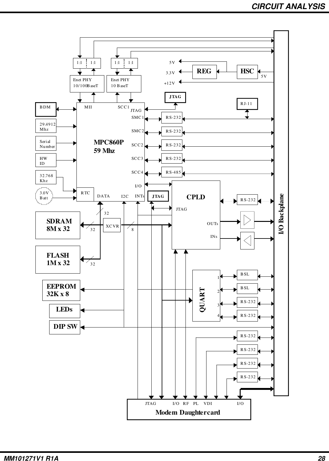
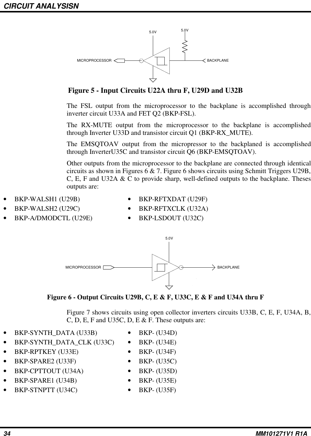
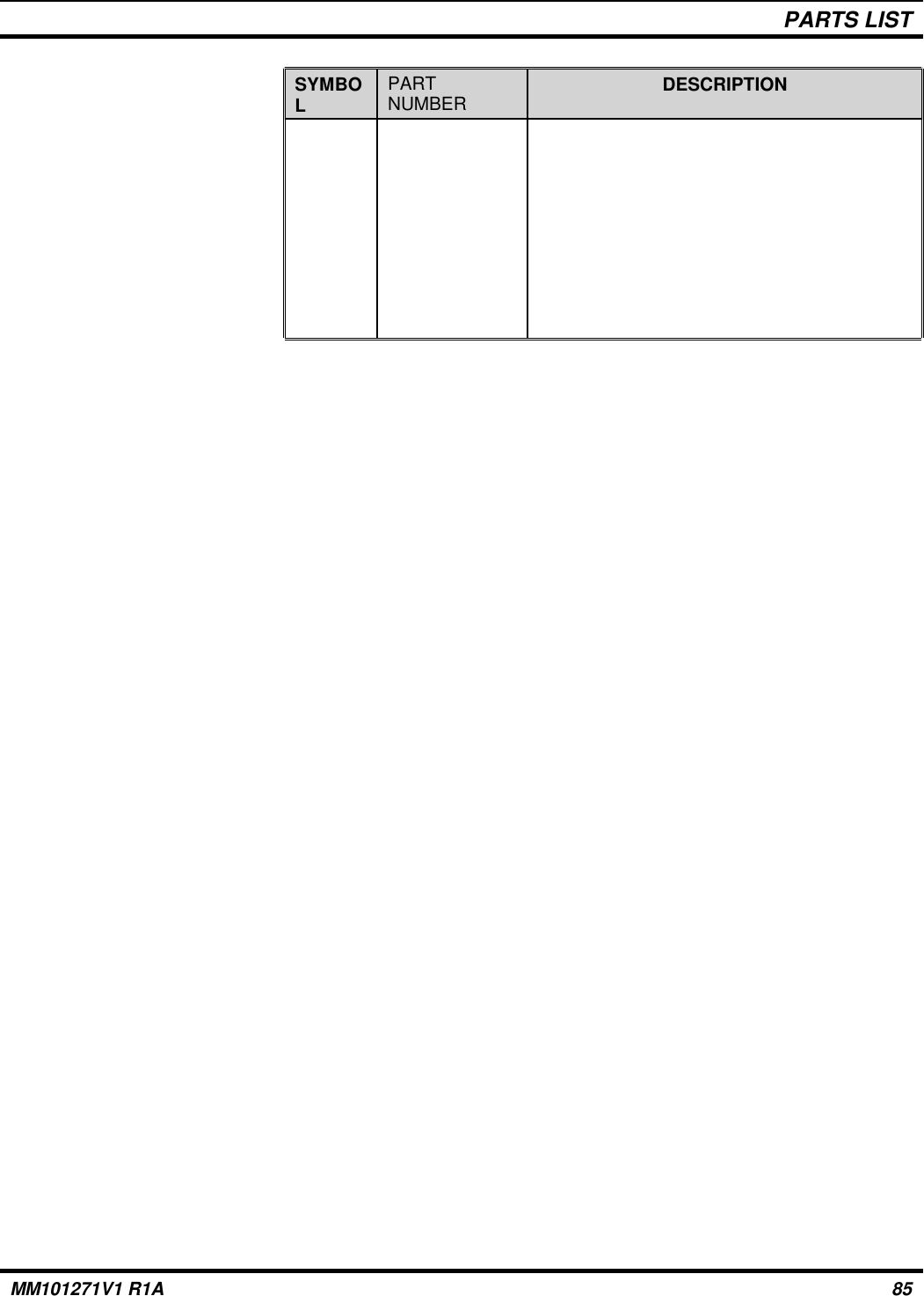
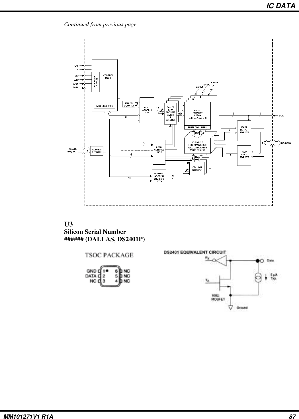
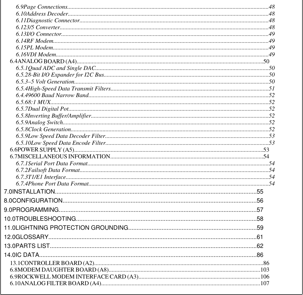
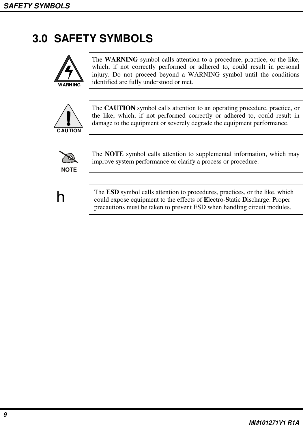
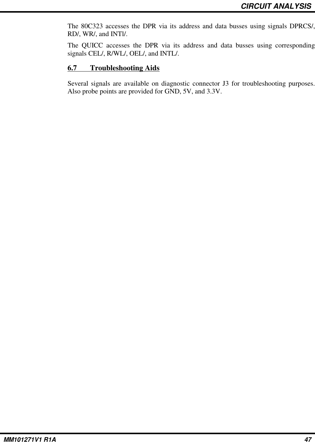
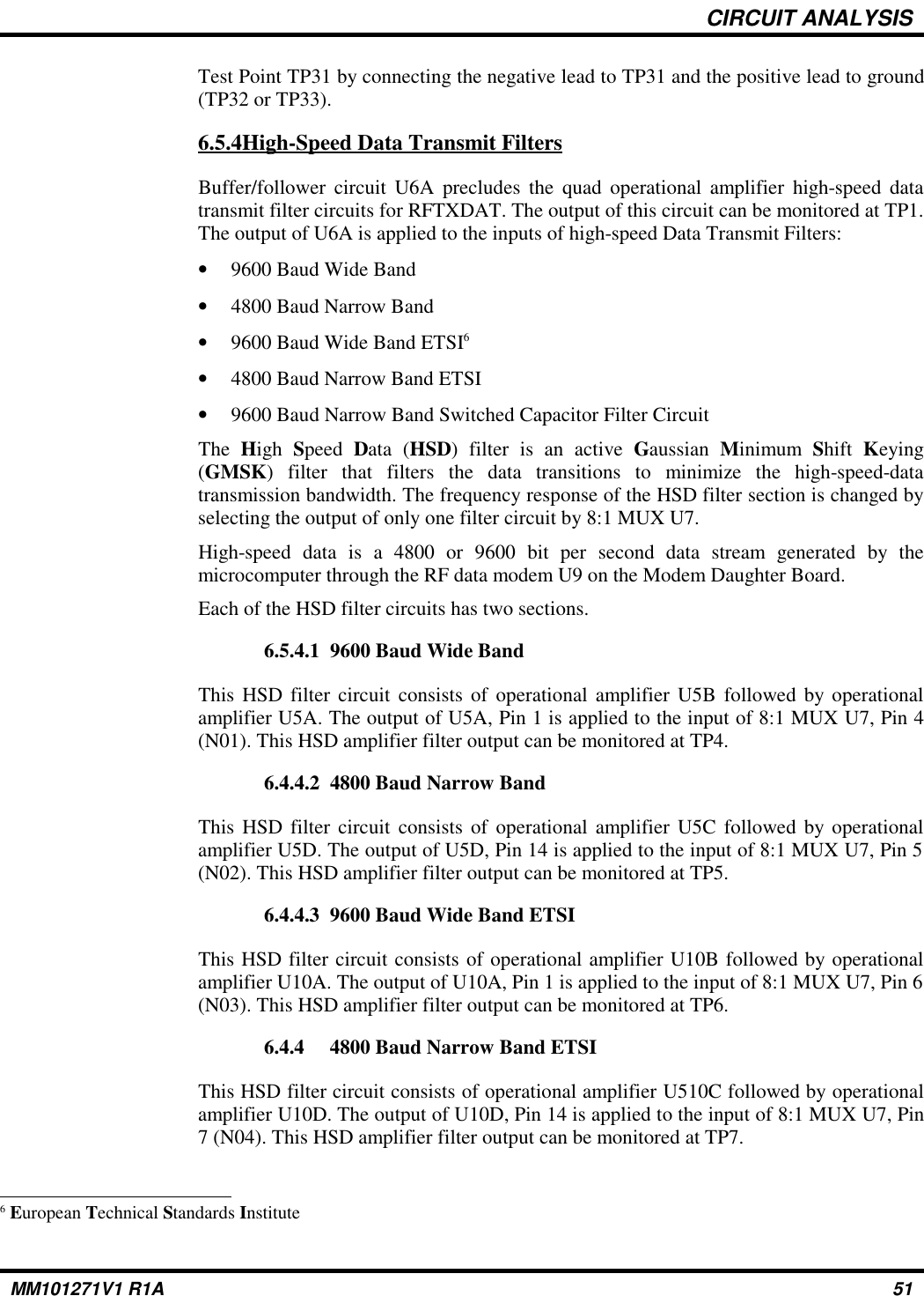
![CIRCUIT ANALYSISDevice IRQ Machine Data Bus WidthQUART INTERRUPT VECTOR CS3 GPCM 8 BitsEPLD CS4 GPCM 8 BitsMODEM DB DUAL PORT RAM CS5 UPMB58 BitsMODEM DB CODE RAM CS6 GPCM 8 Bits(SPARE-EPLD) CS7 N/A N/ANote that there is both a 32-bit data bus and an 8-bit data bus. The 8-bit data bus isconnected to the 32-bit processor data bus via an 8-bit transceiver. The output enable forthe transceiver is controlled by ANDing all 8-bits chips selects together inside the EPLD.6.4.2 Microprocessor SupportThe microprocessor support as shown on Schematic Diagram WP-CB101069V1, Sheet 9includes:•BDM Debug Port Connector •Silicon Serial Number•Power-On Reset Configuration •KAPWR Switch•32 kHz Crystal •8-Bit Bus Transceiver•VDDSYN Filter •MICTOR Logic Analyzer ConnectorsBDM Debug Port ConnectorFor support, microprocessor U9A provides a dedicated serial port (BDM) for connectinga debugger/emulator. A debugger/emulator connected to this port allows a programmerto read/write registers and external peripherals, control program execution, etc. Manydebuggers also have built-in capability to program on-board flash through this port.These serial port pins are brought to 10-pin header J1 using the standard BDM pinoutPower-ON Reset ConfigurationThe Power-On Reset Configuration consists of four octal buffer/drivers U6A, U6B, U8Aand U8B with 3-state outputs. This circuit ensures that at Power-On all circuits are resetto the starting state. Inputs to these circuits are through 10K BUS8 resistor networksRN7 and RN10. The outputs tie into bus D[0.31]. Each package is organized as two 4-bitline drivers with separate output-enable (OE) inputs. These inputs are tied together andconnect to RESET-N. When RESET-N is low, data passes from A inputs to Y outputs.When RESET-N is high, the outputs are in the high-impedance state.32 kHz CrystalThis crystal circuit consist of crystal package Y3, resistors R90 and R98, capacitors C49and C63. This circuits connects to U9A between pins N1 (EXTAL) and P1 (XTAL) andproduces an oscillator frequency of 32.768kHz to drive the real-time clock.5 UPMB is only required if the system makes use of the BUSY_N signal coming from the dual port memory. If BUSY_N isnot used, then a GPCM machine can be used for this chip select.MM101271V1 R1A 37](https://usermanual.wiki/HARRIS/TR-307-A/User-Guide-163371-Page-38.png)

![PARTS LISTSYMBOLPARTNUMBER DESCRIPTIOND1andD2 BAT54LT1D5 Dual High Speed: sim to BAL99.D11andD12Dual High Speed: sim to BAL99D15 BAT54LT1- - - - JACK - - - -J1 DIN96_ABC_R- - - - RELAYS - - - -K1andK2EB2-4.5S- - - - TRANSISTOR - - - -Q1 MMBT3904LT1- - - - RESISTORS - - - -R1 124k OhmsR2 SM/RP_EXB-D10C [EXB-D10C/SM]R3R4 16k OhmsR5 1.21k OhmsR6 5.11k OhmsR7 1k OhmsR8 16k OhmsR9 1.21k OhmsR10 5.11k OhmsR11 1k OhmsR12andR13NMR14 31.6k OhmsR15 0 OhmsR16 150k OhmsR17 100k OhmsR18 1Meg OhmR19 NMR20 1Meg OhmsMM101271V1 R1A 77](https://usermanual.wiki/HARRIS/TR-307-A/User-Guide-163371-Page-78.png)

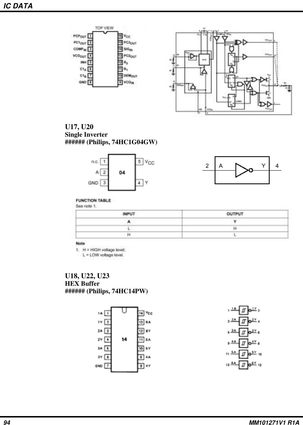
![PARTS LISTSYMBOLPARTNUMBER DESCRIPTIONR123andR12451.1K OhmsR12539.2k OhmsR126332k OhmsR127SM/RP_EXB-D10C [EXB-D10C/SM]R128thruR1300 OhmsR13110Meg Ohms- - - - TEST POINTS - - - -TP32AndTP33TP-107-01 [T POINT R]- - - - INTEGRATED CIRCUITS - - - -U2 : sim to Motorola, MC79M05BT.U3 : sim to Motorola, MC74HC393AD.U4 Remote 16-bit I/O Expander: sim to Philips,PCF8575CTS.U5 : sim to Motorola, MC33074D.U6 : sim to Motorola, MC33072D.U7 Fault-Protected, High-Voltage Single 8-to-1/Dual 4-to-1 Multiplexers: sim to Maxim,MAX4508ESE.U8 : sim to Dallas, DS1803Z-010.U9 SPST/SPDT Analog Switches: sim to Maxim,DG419DY.U10 : sim to Motorola, MC33074DU11 8th-Order, Lowpass, Switched-CapacitorFilters: sim to Maxim, MAX292ESA.U12 : sim to Motorola, LM393D.U13 : sim toU14 : sim to Maxim, MAX294EWE.U15 : sim to Motorola, MC33072D.U16 : sim to Linear Tech, LTC4861S.MM101271V1 R1A 81](https://usermanual.wiki/HARRIS/TR-307-A/User-Guide-163371-Page-82.png)