HARRIS TR-307-A Land Mobile Basestation Transceiver User Manual Manual
HARRIS CORPORATION Land Mobile Basestation Transceiver Manual
HARRIS >
Manual

MM101271V1 R1A
Maintenance Manual
SitePro
Controller Shelf Assembly
EA101209V1

NOTICE!
The voice coding technology embodied in this product is protected by intellectual property rights including patent rights,
copyrights, and trade secrets of Digital Voice Systems, Inc. The user of this technology is explicitly prohibited from
attempting to decompile, reverse engineer, or disassemble the Object Code, or in any other way convert the Object Code
into a human-readable form.
NOTICE!
This manual covers products manufactured and sold by Com-Net Ericsson Critical Radio Systems, Inc.
NOTICE!
Repairs to this equipment should be made only by an authorized service technician or facility designated by the
supplier. Any repairs, alterations or substitution of recommended parts made by the user to this equipment not
approved by the manufacturer could void the user's authority to operate the equipment in addition to the
manufacturer's warranty.
NOTICE!
The software contained in this device is copyrighted by Com-Net Ericsson Critical Radio Systems, Inc. Unpublished
rights are reserved under the copyright laws of the United States.
This manual is published by Com-Net Ericsson Critical Radio Systems, Inc., without any warranty. Improvements and changes to this manual
necessitated by typographical errors, inaccuracies of current information, or improvements to programs and/or equipment, may be made by Com-Net
Ericsson Critical Radio Systems, Inc., at any time and without notice. Such changes will be incorporated into new editions of this manual. No part of
this manual may be reproduced or transmitted in any form or by any means, electronic or mechanical, including photocopying and recording, for any
purpose, without the express written permission of Com-Net Ericsson Critical Radio Systems, Inc.
EDACS is a registered trademark, and Aegis, ProVoice and SitePro are trademarks of Com-Net Ericsson Critical Radio Systems, Inc.
2
MM101271V1 R1A

Copyright August 20001, Com-Net Ericsson Critical Radio Systems, Inc. All rights reserved.
MM101271V1 R1A 3

TABLE OF CONTENTS
TABLE OF CONTENTS Page
MM101271V1 R1A 4

TABLE OF CONTENTS
1.0SPECIFICATIONS1......................................................................................................................7
2.0RELATED PUBLICATIONS.........................................................................................................8
3.0SAFETY SYMBOLS.....................................................................................................................9
4.0INTRODUCTION........................................................................................................................10
4.1APPLICATIONS.......................................................................................................................................10
4.2COMMUNICATIONS..............................................................................................................................11
4.3COMPATIBILITY AND MIGRATION...................................................................................................12
4.4SYSTEM EXTERNAL INTERFACES.....................................................................................................12
4.4.1Station Control.......................................................................................................................................12
4.4.2Simulcast Control...................................................................................................................................14
4.4.3Conventional Control.............................................................................................................................15
4.4.4Voter Control..........................................................................................................................................15
4.4.5Asynchronous Serial Ports.....................................................................................................................16
4.4.6Synchronous Serial Ports.......................................................................................................................16
4.4.7Power.....................................................................................................................................................16
11.DESCRIPTION...........................................................................................................................18
5.1INDICATORS AND CONTROLS............................................................................................................18
5.1.1Indicators...............................................................................................................................................18
5.1.2Controls..................................................................................................................................................19
5.2ROCKWELL MODEM.............................................................................................................................19
5.3LOW SPEED AND HIGH SPEED DATA FILTERS................................................................................20
5.3.1Low Speed Data Decode Filter..............................................................................................................20
5.3.2High Speed Data Encode Filter.............................................................................................................20
5.4INTERFACE CONNECTIONS................................................................................................................20
5.5COMMUNICATION LINKS....................................................................................................................21
6.0CIRCUIT ANALYSIS..................................................................................................................24
6.1SHELF ASSEMBLY.................................................................................................................................24
6.2INTERCONNECT BOARD (A1)..............................................................................................................26
6.3CONTROLLER BOARD (A2)..................................................................................................................26
6.3.1Block Diagram.......................................................................................................................................26
6.3.2System I/O..............................................................................................................................................26
6.3.3Blackplane..............................................................................................................................................32
6.3.4CPU........................................................................................................................................................36
6.3.5Modem Daughter Board Connector.......................................................................................................38
6.4.5Electrically Programmable Logic Device (EPLD)................................................................................39
6.7Ethernet Ports...........................................................................................................................................39
6.4.6I2C Bus...................................................................................................................................................40
6.4.7Memory...................................................................................................................................................41
6.5...................................................................................................................MODEM DAUGHTER BOARD 42
6.1Modems.....................................................................................................................................................45
6.23.3V/5V Interface......................................................................................................................................45
6.3Microprocessor.........................................................................................................................................45
6.4Code Memory............................................................................................................................................46
6.5Data Memory.............................................................................................................................................46
6.6Dual Port Ram..........................................................................................................................................46
6.7Troubleshooting Aids................................................................................................................................47
6.4ROCKWELL MODEM INTERFACE CARD (A3)...................................................................................48
7.0QIUCC Connector.....................................................................................................................................48
6.2Dual Port RAM..........................................................................................................................................48
6.3Microcontroller.........................................................................................................................................48
6.48-bit Latch.................................................................................................................................................48
6.5Address Buffer...........................................................................................................................................48
6.6Data Buffer................................................................................................................................................48
6.7Code SRAM...............................................................................................................................................48
6.8Data SRAM................................................................................................................................................48
MM101271V1 R1A 5

6.9Page Connections......................................................................................................................................48
6.10Address Decoder.....................................................................................................................................48
6.11Diagnostic Connector.............................................................................................................................48
6.123/5 Converter...........................................................................................................................................48
6.13I/O Connector..........................................................................................................................................49
6.14RF Modem...............................................................................................................................................49
6.15PL Modem...............................................................................................................................................49
6.16VDI Modem.............................................................................................................................................49
6.4ANALOG BOARD (A4)............................................................................................................................50
6.5.1Quad ADC and Single DAC...................................................................................................................50
6.5.28-Bit I/O Expander for I2C Bus.............................................................................................................50
6.5.3–5 Volt Generation.................................................................................................................................50
6.5.4High-Speed Data Transmit Filters.........................................................................................................51
6.4.49600 Baud Narrow Band.......................................................................................................................52
6.5.68:1 MUX.................................................................................................................................................52
6.5.7Dual Digital Pot.....................................................................................................................................52
6.5.8Inverting Buffer/Amplifier......................................................................................................................52
6.5.9Analog Switch.........................................................................................................................................52
6.5.8Clock Generation...................................................................................................................................52
6.5.9Low Speed Data Decoder Filter............................................................................................................53
6.5.10Low Speed Data Encode Filter............................................................................................................53
6.6POWER SUPPLY (A5).............................................................................................................................53
6.7MISCELLANEOUS INFORMATION.....................................................................................................54
6.7.1Serial Port Data Format........................................................................................................................54
6.7.2Failsoft Data Format.............................................................................................................................54
6.7.3T1/E1 Interface.......................................................................................................................................54
6.7.4Phone Port Data Format.......................................................................................................................54
7.0INSTALLATION..........................................................................................................................55
8.0CONFIGURATION.....................................................................................................................56
9.0PROGRAMMING.......................................................................................................................57
10.0TROUBLESHOOTING.............................................................................................................58
11.0LIGHTNING PROTECTION GROUNDING.............................................................................59
12.0GLOSSARY..............................................................................................................................61
13.0PARTS LIST.............................................................................................................................62
14.0IC DATA...................................................................................................................................86
13.1CONTROLLER BOARD (A2)................................................................................................................86
6.8MODEM DAUGHTER BOARD (A8)....................................................................................................103
6.9ROCKWELL MODEM INTERFACE CARD (A3).................................................................................106
6.10ANALOG FILTER BOARD (A4).........................................................................................................107

6MM101271V1 R1A

SPECIFICATIONS
1.0 SPECIFICATIONS1
INPUT VOLTAGE +13.8±20% VDC
CURRENT DRAIN
Without 9600 baud modem 900ma (typical), 1.5 Amps (maximum)
With 9600 baud modem 1.5 Amps (typical), 2 Amps (maximum)
OPERATING TEMPERATURE -22°F to +140°F (-30°C to +60°C)
DIMENSIONS (H x W) 1.75 x 19 inches (4.5 x 48.3 cm)
DATA TRANSMISSION
High Speed 9600 ±1bps (EDACS Wideband)
4800 ±1bps (EDACS Narrow band)
Low Speed 150 ±1bps
COMMUNICATION INTERFACE
Site Controller (trunked)
Protocol RS-232C
Data Format 1 start bit, 1 stop bit, and 8 data bits
Data Rate 19.2 kilobaud
Back-up Serial Link (Failsoft)
Data Levels 0 to 13.8 VDC swing (nominal)
Data Format 1 start bit, 1 stop bit, and 8/9 data bits
Data Rate 19.2 kilobaud
1 These specifications are intended to be used by the service technician during servicing. Refer to the appropriate
Specification Sheet for the complete Specification.
MM101271V1 R1A 7

RELATED PUBLICATIONS
2.0 RELATED PUBLICATIONS
The SitePro Controller trunking shelf is used in several applications, broadly including
Voting, EDACS®, Aegis, and Digital Voice. In each of these applications the same
SitePro Controller shelf is used, however, the Logic Board operates differently because
of different jumper configuration, interfacing hardware, and software. Refer to the
appropriate Com-Net Ericsson technical publication for additional information on each
application as follows:
Publication Title
MM101343V1 SitePro Installation Manual
MM#######V1 Rockwell Modem ROA 117 2247
LBI-31981 Digital Voice Voting Tone Board Maintenance Manual
LBI-38462 EDACS Voter Interface Board Maintenance Manual
LBI-38896 EDACS Site Downlink and CEC/IMC Uplink Configuration
Manual
MM#######V1 EDACS Voter Digital Receiver and Selector ProSite
Configuration Manual
LBI-38985 EDACS Site Controller Maintenance Manual
MM#######V1 SitePro Conventional Network Interface (CNI) Configuration
Manual
MM#######V1 EDACS Single Channel Autonomous Trunking (SCAT) SitePro
and Downlink SitePro Configuration Manual
MM#######V1 EDACS Station ProSite Configuration Manual
MM#######V1 EDACS Test Unit and Alarm Interface (TUAI) SitePro
Configuration Manual.
LBI-39004 EDACS Guardog Installation and Operation Manual
MM#######V1 SitePro Shelf Programming Manual
MM101271V1 R1A 8
SAFETY SYMBOLS
3.0 SAFETY SYMBOLS
WARNING
The WARNING symbol calls attention to a procedure, practice, or the like,
which, if not correctly performed or adhered to, could result in personal
injury. Do not proceed beyond a WARNING symbol until the conditions
identified are fully understood or met.
CAUTION
The CAUTION symbol calls attention to an operating procedure, practice, or
the like, which, if not performed correctly or adhered to, could result in
damage to the equipment or severely degrade the equipment performance.
NOTE
The NOTE symbol calls attention to supplemental information, which may
improve system performance or clarify a process or procedure.
hThe ESD symbol calls attention to procedures, practices, or the like, which
could expose equipment to the effects of Electro-Static Discharge. Proper
precautions must be taken to prevent ESD when handling circuit modules.
9
MM101271V1 R1A

4.0 INTRODUCTION
The Com-Net Ericsson Critical Radio Systems group has developed a Motorola
PowerQuicc-based CPU to replace the 8051-based GETC board due to memory
limitations. In addition to replacing the functionality of the GETC module, other
capabilities have been added. including support of ethernet.
This manual provides maintenance and servicing information for Com-Net Ericsson
SitePro Controller Shelf Assembly EA101209V12. Production versions of this shelf
consist of the following components:
•Shelf Assembly MA101080V1
Chassis MA101080V2
•Interconnect Board Assembly (A1) CB101073V1
•Controller board Assembly (A2) CD101069V1
•Modem Daughter Board (A8) CB101074V1
•Rockwell Modem Interface
Card Assembly (A3) ROA 117 2247
Rockwell Modem Assembly (A7) RYTUZ 921 01/1
•Analog Board (A4) CB101070V1
•Power Supply Module (A5) CONDOR DP1719
•Display Module (A6) MA101082V1
Display Board Assembly (A6-A1) CB101077V1
Cable (A6-W1) CA101222V1
•Input Cable to the Power Supply (W1) CA101211V1
•Output Cable from the Power Supply (W2) CA101212V1
•Data Cable (W#) CA101213V1
4.1APPLICATIONS
The SitePro Controller can be installed and programmed for several different station
applications. The basic programming is for the Station Trunking Shelf. This shelf
enables the station to function as part of an EDACS trunked communication system by
providing digital signaling and transmitter control of the associated base station. In
addition, the SitePro Controller provides an interface between the base station repeater,
the Site Controller or Site Interface Module (SIM) and other channel SitePro
Controller(s) at the same time.
By reconfiguring the SitePro Controller shelf hardware and programming the operation
through the programming port, located on the front panel, the SitePro Controller can be
used as an/a:
•Uplink/Downlink – Configured as either an Uplink or Downlink, the SitePro
Controller provides the communications link between the Transmit Site and the
CEC/IMC switch.
2The Service Technician(s) should always consult application manuals, Software Release Notes (SRN), and Specific
Customer information provided with the system whenever the equipment requires service or repair.
10 MM101271V1 R1A

•SCAT –TheSitePro Controller can be programmed to provide command and
control of a Single Channel Autonomous Trunking (SCAT) Site.
•CNI –ProgrammedasaConventional Network Interface (CNI), the SitePro
Controller provides the communication link between a conventional
communications site (analog) and an EDACS trunking system (digital).
•Satellite Receiver –TheSitePro Controller can be programmed to provide
command and control of Satellite (Auxiliary) Receivers and communication to the
Voter Digital Receiver.
•Voter Digital Receiver –TheSitePro Controller can be programmed to process
digital data from Satellite Receiver SitePro Controller(s) for input to the Voter
Selector.
•Voter Selector –TheSitePro Controller can be programmed to control the voting
processes and select the sites with the best signals.
•VDI – Programmed as a Voter Digital Interface, the SitePro Controller provides a
path for Voter and Simulcast systems to the Jessica PBX system when making digital
calls.
•Simulcast Control Point and Tx Site – The SitePro Controller can be
programmed to provide Simulcast system command and control.3
4.2COMMUNICATIONS
The following communication modes are available:
1. The SitePro Controller can communicate with Personal Computers (PC’s) through
ethernet ports J5 and J6.
2. The SitePro Controller can communicate with other devices, such as Site
Controllers or the CEC/IMC switch, through the Serial Ports at J14, using an RS-232
serial data format operating at 19.2 kilobaud. Connector J14 provides connection to 6
telephone lines and 6 serial ports.
3. The SitePro Controller can communicate with other SitePro Controller(s) in the
Failsoft or Enhanced mode, over two Backup Serial Links (BSL)ortwoRockwell
Modems (RM’s) through connector J4. This link uses 0-13.8 VDC levels at 19.2
kilobaud.
4. The SitePro Controller uses the Frame Sync Line (FSL), also through connector
J4, to communicate timing between SitePro Controllers. This line uses a 0-13.8
VDC bus that carries a periodic negative pulse.
5. A 9600 or 4800 baud full-duplex, synchronous communication interface over an RF
Channel.
6. The SitePro Controller can use synchronous modem data to communicate with
other sites via telephone lines or microwave links.
7. The SitePro Controller interfaces with an Enhanced Digital Access Communication
System (EDACS) through 24 Pin connector J12.
8. Power is connected to the SitePro Controller through 4 Pin POWER connector J7.
3 Installation and configuration of Simulcast SitePro Controllers is documented in a specific Simulcast Application Manual.
MM101271V1 R1A 11

9. The SitePro Controller interfaces with a Conventional MASTR III base station or
Digital Signal Processor (DSP) through 20 Pin CONV/DSP connector J11.
10. The SitePro Controller interfaces with a GPS Simulcast system through 26 Pin
SIMULCAST connector J13.
NOTE
SitePro Controller interface functions vary from application to application and
between EDACS systems using MASTR II or MASTR III repeaters. It is necessary to
refer to the Application Configuration Manual for details regarding the specific
hardware and software configuration of the SitePro Controller.
4.3 COMPATIBILITY AND MIGRATION
The SitePro Controller is compatible with Generic EDACS Trunking Card (GETC)
compatible devices with the exception of the Site Controller.
The requirements are that the SitePro Controller will only switch modes if the Control
Channel fails or a configuration command is received. The SitePro Controller will,
however, change modes as currently implemented by the GETC. For example, the
SitePro Controller Control Channel can switch modes, without failure or configuration
command, if it detects carrier.
For High Speed Data Modulation,theSitePro Controller has a separate Analog Board
(A4) providing software configurable filtering, which is compatible with high speed data
types.
4.4 SYSTEM EXTERNAL INTERFACES
(SitePro Trunked Interface Specification)
The following is a description of all electrical connections to the SitePro Controller.
All input/output definitions are relative to the SitePro Controller. This configuration
supports EDACS and Simulcast. The analog and digital control signals provide an
interface to a variety of base stations and are grouped by functionality.
4.4.1 Station Control
•LocRxAudio - Analog input
MASTR III level = 1 Vrms, Zin = 100Kohm, bias = ac coupled
MASTR IIe level = .750 Vrms
This signal is unfiltered local receiver audio from the base station also called
Volume/Squelch or VolSq and carries either High Speed Data (control
signaling/digital audio) or Low Speed Data with analog audio. The two components
are internally separated.
•RUS - Digital TTL active high input
This signal is the Receiver UnSquelch signal from the base station and is activated
when a carrier of sufficient signal strength (as determined by the squelch pot setting)
is present.
•LSD - Analog output
level = 775 mVrms, Zout = 100ohm, bias = 0 volts
12 MM101271V1 R1A

This signal is the Low Speed Data output to the base station. The signal is
conditioned through a low pass filter to remove frequency components above 300 Hz
to allow multiplexing with analog voice audio.
•HSD - Analog output
level = 775 mVrms, Zout = 100ohm, bias = 0 volts
This signal is the High Speed Data output to the base station modulator. The signal is
conditioned through a specially designed filter needed to meet precise RF
modulation bandwidth limitations.
•LocPTT - Digital active low open collector output
This signal is the Local PTT control. This line, when low, will key up the base
station transmitter and select the local receiver audio source for transmission.
•RemPTT - Digital active low open collector output
This signal is the Remote PTT control. This line, when low, will key up the base
station transmitter and select the remote audio source for transmission.
•A/DmodCtrl - Digital output TTL
This is the Analog/Digital Modulation Control signal. When high, HSD is routed to
the base station transmit. When low, LSD/audio is routed to the base station
transmit.
•HSAcq - Digital output open collector output
This is the High Speed Acquisition control signal. A high or low signal produces a
corresponding high or low time constant in the limiter circuit.
•LocRxMute - Digital active low output (8.5 volt low Z source)
This signal is the Local Receiver Mute control. This line, when low, blocks the
routing of receiver audio to the base station transmitter and line out. Muting occurs
during HSD transmission, no valid carrier present, or no valid LSD present.
•Walsh1/Walsh2 - Digital output TTL
These two signals are combined to form a two bit Walsh Function DAC. This signal
is the Low Speed Data source.
•Synth_Clk – Digital open collector output
This signal provides the clock source for loading the base station frequency
synthesizer (required for MIIe). Data is clocked on the negative edge of the clock.
The baud rate is approximately 2.4Kbaud.
•Synth_Data – Digital open collector output
This signal provides the data source for loading the base station frequency
synthesizer (required for MIIe). Data is clocked on the negative edge of the clock.
The baud rate is approximately 2.4Kbaud.
•Synth_LdEn – Digital open collector output
This signal is the Synthesizer Load Enable control. This line, when high, permits the
base station frequency synthesizer to be loaded and is used for protection against
invalid transitions on the clock and data lines.
•Synth_Locked – Digital TTL active high input
MM101271V1 R1A 13

This is the Synthesizer Locked signal. This line, when high, indicates that the base
station synthesizer is locked. This is used for verifying successful synthesizer
loading and is also continuously monitored as a failure mode.
•PAFail - Digital TTL active high input diode isolated with pullup
This is the Power Amp Failure indicator. This line, when high, indicates that the
base station PA has failed. A floating line asserts PA Fail.
•RemAudioFlag - Digital TTL active low input, diode isolated
This is the Remote Audio Present indicator. This line, when low, indicates that
remote audio from the IMC is present. This is generated by the base station in
response to 2175Hz or E&M from the IMC.
•FSL - Digital open drain bi-directional
output: 100 mA sink (low), 10mA source (high)
input: Zin = 1Kohm
This is the bi-directional Frame Sync Line. The line is used as an output in the
Control Channel and as an input in the Working Channel.
•ADCin – Analog input
level = 0 to 5 volts, Zin = 100Kohm
This is the 8-bit Analog to Digital Converter (ADC) input. This may be used to
monitor station PA power.
4.4.2 Simulcast Control
•ext_PTT - Digital TTL active low input, diode isolated
This is the external source for Local PTT and is only active in a Simulcast
configuration.
•ext_A/Dmodctrl - Digital TTL active low input, diode isolated
This is the external source for the Analog/Digital modulation control and is only
active in a Simulcast configuration.
•ext_150 - Digital TTL active low input, diode isolated
This is the external source for Low Speed Data and is only active in a Simulcast
configuration.
•ext_9600baud - Digital TTL active low input, diode isolated
This is the external source for High Speed Data and is only active in a Simulcast
configuration.
•bypass - Digital TTL active low input, diode isolated
This is the Simulcast bypass control signal. This line, when low, forces the site to
operate in non-Simulcast mode and is driven by the Simulcast control equipment.
•inhibit - Digital TTL active low input, diode isolated
This signal is the Simulcast alarm indicator. This line, when low, indicates the
presence of a Simulcast alarm and is driven by the Simulcast control equipment.
•txclk_in - Digital TTL active low input, diode isolated
14 MM101271V1 R1A

This is the external source for High Speed Clock and is only active in a Simulcast
configuration.
•txclk_alarm - Digital TTL active high output
This signal is the Simulcast Tx Clock alarm indicator. This line, when high, indicates
that the external source for High Speed Clock is missing and is only active in a
Simulcast configuration.
4.4.3 Conventional Control
•CPTT – Digital open collector output
This signal is the Combined PTT control. This line, when low, will key up the base
station transmitter.
•TxCGDis – Digital open collector output
This signal is the Transmit Channel Guard Disable control. This line, when low,
prevents the transmission of Channel.
•CGMon - Digital TTL active low input, diode isolated
This signal is the Channel Guard Monitor control.
4.4.4 Voter Control
•vot_emsq - Digital open collector output
This is the Voter E&M Squelch signal. This line, when low, indicates the presence
of E&M from the Voter.
•vot_rcvng - Digital active low input
This is the Voter Receiving signal. This line, when low, indicates that the Voter is
receiving.
MM101271V1 R1A 15
INTRODUCTION
4.4.5 Asynchronous Serial Ports
The following asynchronous serial ports provide control links to the SitePro.
Table 1 –Asynchronous Serial Ports
Port Format Function
ENet0 Ethernet 10baseT Management
ENet1 Ethernet 10baseT Spare
SCC1 RS232 19200 8N1 MASTR III
SCC2 RS232 19200 8N1 Spare
SCC3 RS485 Spare
Com1 BSL 38400 8N1 BSL
Com2 BSL 38400 8N1 BSL
Com3 RS232 19200 8N1 Spare
Com4 RS232 19200 8N1 Spare
SMC0 RS232 19200 8N1 Program/Debug
SMC1 RS232 38400 8N1 Spare
4.4.6 Synchronous Serial Ports
The following synchronous serial ports provide data and control paths from the SitePro
to the base station (High Speed Data), to the IMC (Phone Line), and to optional Voter
equipment (VDI).
Note that SSP0 is a new interface port providing unfiltered high speed data to/from a
DSP based modulator.
Table 2 - Synchronous Serial Ports
Port Format Function Signals
SSP0 4800/9600 baud Local (RF)
Comm Link TxData, TxClock
RxData, RxClock
SSP1 9600 baud Remote (PL)
Comm Link TxData, TxClock
RxData, RxClock
CTS, RTS
SSP2 9600 baud Voter (VDI)
Comm Link TxData, TxClock
RxData, RxClock
CTS, RTS
4.4.7 Power
•+13.8V - power supply input
+13.8 volts, 1.5 amps (nominal), input range 10 to 30 volts
This signal is the positive voltage supply for the SitePro Controller and should be
MM101271V1 R1A 16

INTRODUCTION
externally fused. An internal switching DC-DC converter will be used to supply +/-
12 and +5volts to the SitePro Controller sub-components.
•GND – power supply input
This signal is the ground connection for the SitePro Controller.
MM101271V1 R1A 17

DESCRIPTION
11.DESCRIPTION
The SitePro Controller is essentially a processor with audio filtering and specialized
I/O capability. Flexibility in design allows the SitePro Controller to be configured to
function in many applications as suggested in the INTRODUCTION. Except for
Configuration Data, the SitePro Controller software is stored in flash memory.
Configuration Data is stored in NOnVolatile Random Access Memory (NOVRAM).
The Controller Board, Rockwell Modem, Analog Board, Power Supply, Display Module,
and Display Board are mounted on a tray and enclosed in a slide-out shelf (Figure 1).
The SitePro Controller shelf is a one-rack unit assembly (1.75-inches x 19-inches),
which mounts in a standard 19-inch wide equipment cabinet/rack.
Controller Board A2 uses Dual High Speed Diodes BAV99’s for lightning protection on
all RS-232C inputs and outputs. However, maximum lightning protection is achieved
when the SitePro Controller is grounded to the cabinet earth-ground using Lightning
Protection Circuitry Ground Kit 344A4500 and the Cabinet Grounding strap Kit
344A4730. Specific details for installing these grounding kits are found in the
LIGHTNING PROTECTION section LIGHTNING PROTECTION GROUNDING
of this manual.
5.1INDICATORS AND CONTROLS
This section describes the indicators and controls visible and accessible from the front
panel of the SitePro Controller Shelf Assembly.
There are two hinged doors on the front panel of the shelf assembly. Each door has a
window so that indicators mounted on Control Board A2 and Rockwell Modem Interface
Card A3 can be seen. Opening the Control Board door provides access to Reset
Pushbutton switch S1. This door also provides access to PROGRAMMING SERIAL
PORT J8. The circuit boards can be removed from the shelf assembly through these
doors. An extender card can be inserted providing access to a board in a hot system.
5.1.1 Indicators
5.1.1.1 Controller Board Power Indicator
Green LED indicator D12 provided on the Controller Board indicates when power is
applied to the shelf. This indicator is visible through the window in the hinged door on
the front panel of the shelf.
5.1.1.2 Controller Board Status Indicators
Four Red LED status indicators L1 thru L4 (D1 thru D4) are visible through the window
in the hinged door. These indicators show the state of operation of the SitePro
Controller. The interpretation of these indicators depend on the system application
(refer to the SitePro Controller configuration manual for the specific application).
Green ETHERNET indicators ETH0 and ETH1 are also visible through the window in
the hinged door. These indicators indicate when something is connected to ETHERNET
1 or ETHERNET 2 ports.
MM101271V1 R1A 18

DESCRIPTION
There are six other LED indicators on the Controller Board that are not visible unless the
board is on an extender board. Yellow LED’s D7 and D10 indicate when there is
transmit activity. Yellow LED’s D6 and D9 indicate when there is receive activity.
Green LED’s D5 and D8 indicate when there is link activity (refer to the 10 Base-T
Transceiver section and the 10/100 Base-T Transceiver sections).
5.1.1.3 Rockwell Modem Interface Card Indicators
There are five Red LED indicators on Rockwell Modem Interface Card A3. These LED’s
are visible through the window in the hinged door and indicate +5V, +12V, -12V, RLDS
and CTS respectively.
5.1.1.4 Display
Eight-digit LED Display Board A6-A1 mounts between the two hinged doors on the
front panel of the SitePro Controller Shelf Assembly. Green LED D1 indicates
POWER ON to the Display Board. This display displays Channel Status and Channel
Information.
5.1.2Controls
Reset Pushbutton Switch S1 is the only control available on the front panel of the
SitePro Shelf Assembly. It is used to restart the logic of the SitePro Controller.Itis
especially useful when a circuit board has been hot swapped.
5.2ROCKWELL MODEM
The 9600 Baud Rockwell Modem Board RYTUZ 921 01/1 mounts on top of Modem
Interface Card A3 (ROA 117 2247). This Modem Board is used to generate a fast-train,
synchronous, serial data stream suitable for transmission over audio (phone) line or
microwave link. The data stream is sent to a full-duplex, four-wire, dedicated 3002 grade
telephone line.
Controller Board A2 (CB101069V1) controls the associated modem to provide a high
speed synchronous serial interface between the SitePro Controller and other EDACS
elements. Receive and Transmit Phone Data Lines are two balanced pairs carrying
Modem data to and from the station where the data is combined with station audio
(voice) and routed to the Remote Line input and Line output.
In addition to transformer isolation and conditioning provided by the SitePro
Controller, the modem provides automatic adaptive signal equalization, allowing normal
operation using input signal levels from -40 dBm to 0 dBm. The Rockwell Modem
demodulates the input signal and the resulting data is transferred using a serial interface
between the Rockwell Modem and the controller.
The modem senses a received signal by initiating a training state upon detecting an
increase in the input signal level. The modem begins processing data at the end of the
training state if the input signal is still above the nominal -40 dBm receiving threshold
value. Otherwise, the modem returns to an idle mode at the end of the training state if the
input signal is below the nominal receiving threshold value.
MM101271V1 R1A 19
DESCRIPTION
The duration of the modem training state is determined through control signals at the
time of power up. Resetting the SitePro Controller (pressing S1) or cycling the SitePro
Controller shelf operating power, initializes the Rockwell Modem for proper operation.
5.3LOW SPEED AND HIGH SPEED DATA FILTERS
The SitePro Controller has software configurable high speed and low speed data filters.
These filters are configured based on personality data.
5.3.1Low Speed Data Decode Filter
The Low Speed Data (LSD) Decode Filter, part of Analog Logic Board A4, provides
additional filtering to remove voice-audio from the receiver unfiltered audio (vol/sq hi),
thus leaving only the low-speed subaudible data for input to the microprocessor.
5.3.2High Speed Data Encode Filter
The High Speed Data (HSD) Encode Filter, part of Analog Logic Board A4, selects only
the high-speed data (4800 or 9600 baud) from the receiver unfiltered audio (vol/sq hi).
This data can be control signaling or digital voice. The data is processed by the RF
modem and passed on to the microprocessor.
5.4INTERFACE CONNECTIONS
Table 3 - Interface Connections
Connector Interface Connections
J1 32 Pin connector interfaces with Controller Board CB101069V1.
J2 32 Pin connector interfaces with Analog Board CB101070V1.
J3 32 Pin connector interfaces with Rockwell Modem Interface Card ROA
117 2247.
J4 2 over 2 BSL/RM (Rockwell Modem). This connector consist of four
RJ11 connectors as follows:
RM 0 BSL 1
QUART A
RM 1 BSL 0
QUART B
J5 Eithernet 0. Connects to external PC’s.
J6 Eithernet 1. Connects to external PC’s
J7 4 Pin Power connector (+13.8 VDC).
J8 Programming connector on the front of Controller Board A2
J9 Power Supply Output +12V, -12V and +5V. Cable W2 connects
between J9 and J2 on Power Supply Module A5
J10 Connects through cable A6-W1 to Display Module A6.
J11 20 Pin connector for interfacing with a Conventional/DSP system.
20 MM101271V1 R1A
DESCRIPTION
Connector Interface Connections
J12 24 Pin connector for connecting to an Enhanced Digital Access
Communication System (EDACS)
J13 26 Pin connector for interfacing with a Simulcast System.
J14 6 over 6 phone lines and serial ports. This connector consists of twelve
RJ11 connectors as follows:
RM 0 QUART C SCC4
RS 485 SCC3 80C323
PORT 0 N/U
RM 1 QUART D SCC2 SMC2 80C323
PORT 1 N/U
5.5COMMUNICATION LINKS
Communication Modes available to the SitePro Controller are:
1. The SitePro Controller can communicate with other devices such as the Site
Controller, IMC, and RF Station. Communication occurs primarily through an RS-
232C serial interface normally operating at 19.2 kilobaud. for a SitePro Controller
interfacing with a Site Interface Module (SIM) this is set to 38.4 kilobaud.
2. The SitePro Controller can communicate with other SitePro Controllers in the
Failsoft mode of operation, over a Backup Serial Link (BSL). The link uses 0-13.8
VDC levels and operates at 19.2 kilobaud and is ordinarily used in a bus
configuration. For a SitePro Controller interfacing with a SIM this is set to 38.4
kilobaud.
3. A timing signal called the Frame Sync Line (FSL) helps arbitrate the use of the BSL
serial bus in the Voter configuration. The FSL is also used for timing purposes. In
the the station configuration, FSL signals use 0-13 VDC levels to produce a periodic
negative going pulse.
4. A 9600/4800 baud full-duplex, synchronous communication interface over an RF
channel.
5. A 9600 baud phone line or microwave communication interface (this may be RS-232
or modem data) through a Rockwell Modem.
NOTE
SitePro Controller interface functions vary from application to application and
between EDACS systems using MASTR IIe or MASTR III repeaters. It is necessary to
refer to the Application Configuration Manual for details regarding the specific
hardware and software configuration of the SitePro Controller.
MM101271V1 R1A 21
DESCRIPTION
4-Pin POWER, 20-Pin CONV/DSP
& 20-Pin SIMULCAST Connectors
24-Pin EDACS, 4-Pin POWER &
20-Pin CONV/DSP Connectors Ethernet, SERIAL PORT &
BSL/RM Connectors
Back Views
Top View
Front View
MM101271V1 R1A 22
Interc
o
Board
Analog
Board (A4)
Controller
Board (A2)

CIRCUIT ANALYSIS
Figure 1 - SitePro Controller Shelf Assembly
MM101271V1 R1A 23
Modem Daughter Board Power Supply (A5)

CIRCUIT ANALYSIS
6.0 CIRCUIT ANALYSIS
The Theory of operation of each circuit board/card and module used in SitePro
Controller Shelf Assembly EA101209V1 is described in the following paragraphs.
Refer to the Block Diagram in Figure 2 and Outline and Schematic Diagrams as listed in
the TABLE OF CONTENTS.
The SitePro Controller is a Base Station Controller with redundant communication
links [Backup Serial Links (BSL’s)]. The BSL’s provide for inter-channel
communication with two 10Mbit Ethernet Ports. The BSL’s provide trunking
communications as well as site configuration and database messaging. One Ethernet port
is dedicated to Management System information. The second Ethernet Port is not
supported at this time.
The SitePro Controller and System Interface Module (SIM) will use the primary BSL
for trunking information and limited management system information. The secondary
link will ensure continued trunking operation in the event of a primary BSL failure
The SitePro Controller/base station interface for digital information, both receive and
transmit, is 9.6k baud synchronous data. Additional digital control information is
provided via discrete I/O at both the base station and controller. The following diagram
(Figure 2) is a high level picture of the SitePro Controller and external interfaces.
The SitePro Controller, main controller board (A2) and AMPS modem board, replaces
the CPTC GETC.
6.1SHELF ASSEMBLY
SitePro shelf Assembly EA101209V1 is a 19” Rack Mount, one Rack Unit device. It is
enclosed to reduce emissions and interference with other devices. Serial, Ethernet,
power, and I/O connections are accessible at the back of the shelf (Figure 1). The Serial
connections (6 OVER 6 PHONE LINES & SERIAL PORTS) are stacked, two high
using RJ type connectors (J14). The Ethernet connectors J5 & J6 (ETHERNET 0 &
ETHERNET 1) are single height RJ connectors. The power connector (J7) and I/O
connector (J#) are Molex type.
The front panel has two hinged access doors for insertion/removal of the Controller
Board and the Rockwell Modem card for troubleshooting and ease of maintenance.
These doors have RF fingers to reduce emissions. Diagnostic LED’s and the eight-digit
display are viewable from the front panel.
The Shelf Assembly consists of Interconnect Board A1, which provides connectors to
accommodate:
•Controller Board CB101069V1 (A2)
•Rockwell Modem Interface Card Assembly ROA 117 2247 (A3)
•Analog Board CB101070V1 (A4)
•Power Supply DP1719 (A5)
•Display Module MA101082V1 (A6)
MM101271V1 R1A 24
CIRCUIT ANALYSIS
Loc PTT
Rem PTT
A/D ModCtrl
HSD
LSD
PA Fail
Local Rx Audio
Local Tx Audio
RUS
Rem Audio Flag
Local Rx Mute
Synth_Locked
Synth_Clk
Synth_Data
Synth_LdEn
ADCin
bypass
inhibit
ext_PTT
ext_ADModCTrl
ext_150
ext_HSD
TxClk_in
TxClk_alarm
E0
E1
SCC1
SCC2
SCC3
SMC1
BSL/FSL0
BSL/FSL1
Com3
Com4
SP0
SP1
Controller
Analog
Power Supply
(switch mode)
SSP0
SSP1
SSP2
External (simulcast)
Signals and Control
Conventional
Signals and Control
Local (station)
Signals and Control
Voter
Signals and Control
Local (RF) HSD
SitePro Interface
FILTERS
LINE DRIVERS
ANALOG SWITCHES
ADC
MPC860
DS80C323
QUART
USRT
PLD
+5v @2a
+/- 12v
EtherNet Ports
Asynchronous
Serial Ports
RMIC
ROCKWELL MODEM
LINE DRIVERS
ANALOG SWITCHES Voted (VDI) HSD
Remote (PL) HSD
CPTT
TxCGDis
CGMon
Vot_emsq
Vot_rcvng
MM101271V1 R1A 25

CIRCUIT ANALYSISN
Figure 2 - SitePro Shelf Assembly Block Diagram
6.2INTERCONNECT BOARD (A1)
Interconnect Board CB101073V1 is a passive printed circuit board that provides
interconnections between all internal components of the SitePro Controller shelf and
interfaces the SitePro Controller shelf with the outside world (Refer to Table 3 -
Interface Connections, and Interconnection,Outline and Schematic Diagrams). Pi
filters U1 thru U29 eliminate any Electro Mechanical Interference (EMI).
6.3CONTROLLER BOARD (A2)
Controller Board CB101069V1 contains all SitePro Controller logic and control
functions except the power supply and Rockwell Modem (Refer to the Outline and
Schematic Diagrams for the Controller Board as listed in the TABLE OF
CONTENTS).
This Controller Board is based on an MPC860 microprocessor, the primary
responsibility being message processing. This board has multiple high-speed serial ports,
two of which are used for primary and secondary BSL’s. It has hardware and dual port
RAM to support the Modem Board and a 10/100 Mbit ethernet port. This port is
available for Voice Over IP traffic. A second 10 Mbit ethernet port is available for
management functions.
This board has sufficient memory to support 1M LID’s and 64k GID’s. It has LID and
GID validation for all calls.
6.3.1Block Diagram
Figure 3 – Controller Board Block Diagram shows the connection of major components
from a high level viewpoint. Schematic Diagram WD-CB101069V1, Sheet 2 also
provides a Block Diagram for the Controller Board. These diagrams show the major
components of this board as:
•CPU (MPC860P) •Memory
•Eithernet 10 Base T •Electronically Programmable Logic Device
(EPLD)
•Eithernet 10/100 Base T •Quad UART (QUART)
•EEPROM •Interconnect Board
•Daughter Board
6.3.2System I/O
The System I/O circuits for the Controller Board are shown on Schematic Diagram WD-
CB101069V1, Sheet 3 and include:
•Oscillator For PHY’s •3.3V Power Monitor
•JTAG Port •Test Points
•Board Insert Detection Circuit •Programming Serial Port J8
26 MM101271V1 R1A

CIRCUIT ANALYSIS
•Hot Swap Controller •Decouplers
•3.3V Regulator
MM101271V1 R1A 27
CIRCUIT ANALYSIS
MII
Enet PHY
10/100 BaseT
1:1 1:1
SDRAM
8M x 32
FLASH
1M x 32
I2C
EEPROM
32K x 8
32.768
Khz
RTC3.0V
Batt
MPC860P
59 Mhz
29.4912
Mhz
SMC1
SMC2
SCC4
BDM
QUART
RJ-11
RS-232
RS-232
CPLD RS-232
I/O Backplane
1
2
3
4
RS-232
RS-232
Modem Daughtercard
OUTs
INs
32
32
32
8
JTA G
INTsDATA
REG 5V
3.3V
PL I/O
JTAG
JTAG
I/O
+12V
Enet PHY
10 BaseT
1:1 1:1
SCC1
LEDs
VDI
RS-232
RS-232
RF
RS-232
RS-232
DIP SW
RS-232SCC2
RS-232
SCC3
I/O
Serial
Number
HW
ID
RS-485
BSL
BSL
XC VR
JTAG
5V
HSC
JTAG
MM101271V1 R1A 28

CIRCUIT ANALYSIS
Figure 3 - Controller Board Block Diagram
MM101271V1 R1A 29

CIRCUIT ANALYSIS
6.2.1 Oscillator For Ethernet PHY’S
This circuit consists of crystal oscillator circuit Y1 powered by 3.3 V applied to Y1, Pin
4, Vcc. Oscillator circuit Y1 is biased on by resistor R49 connected to Y1, Pin 3, CTRL
and produces 25 MHz on the output at Pin 3 through resistor R51 (OSC 25MHz). This
output connects to the CLK25 inputs to the Ethernet 10 and Ethernet 10/100 Mbit
PHY’s4.
6.2.2 JTAG Port
This JTAG PORT circuit consists of buffer U1 (NC7SZ125M5). This circuit allows
programming directly to a microprocessor through connector J4.
The JTAG port is also routed to the Modem Daughterboard. This allows a future modem
daughterboard to be designed with an Altera EPLD. If that future EPLD modem
daughterboard is used, resistor R187 (0 ohms) must be removed from the board.
6.3.2.3.1Board Insert Detection Circuit
This circuit consists of NPN transistors Q6 and Q7. When the Controller Board is
inserted into a live Interconnect Board, the base circuits of these transistors are
connected to ground through connector J1B, Pins B1 and B32. Connector J1B, Pin B1 is
MATE-DETECT-A and J1B, Pin B32 is MATE-DETECT-B. With the base of both
transistors at ground, they are held in the off state. This allows POWER ON to cycle
high and low as the result of 555 timer U40 running at a programmed rate. The POWER
ON voltage is applied to Pin 2 of Hot SwapTM Controller U37. If the base of either
transistor (Q6 or Q7) is not connected to ground, POWER ON will not be applied to the
HotSwap Controller.
6.2.4 Hot Swap™ Controller
Hot Swap™ controller (HSC) U37 allows Controller Board CB101069V1 to be safely
inserted in or removed from Interconnect Board CB101073V1 while voltage is applied.
Using external N-channel pass transistor Q5, the supply voltage to the Controller Board
is ramped up at a programmable rate. A high side switch driver controls the N-channel
gate for supply voltages ranging from 2.7V to 12V. A programmable electronic circuit
breaker protects against shorts. The RESET output (U37, Pin 1) is used to generate a
system reset when the supply voltage falls below the programmable voltage. The
POWER ON input to U37, Pin 2 is used to cycle the Controller Board power or to
generate a soft reset.
6.2.5 3.3V Regulator
The microprocessor is provided with 5 Volts and ±12 Volts from the Interconnect Board.
Linear regulator U25 is used to provide 3.3 volts to be used by the majority of digital
logic on the Controller Board and the Daughter Board.
The Hot Swap Controller (HSC) is used to ramp up the 5V power rail at a controlled
rate. This, in addition to other considerations, will allow the Controller Board to be hot-
swapable. The 5V output from this circuit will also power the 3.3 Volt regulator, thus
4 PHY is an Industry Standard for “Physical Interface.”
MM101271V1 R1A 30

CIRCUIT ANALYSIS
causing the 3.3 V power rail to also ramp up at a controlled rate. As mentioned above,
the HSC has a built-in electronic circuit breaker. The 555 timer circuit (U40) is
connected to the HSC chip so that the HSC can be automatically reset in the case of a
circuit breaker fault.
6.2.6 3.3V Power Monitor
The 3.3V Power Monitor (U31) uses a precision temperature-compensated reference and
comparator circuit to monitor the status of the 3.3V supply. If a loss of power is detected
an internal power-fail signal forces reset to the active state, which is low. When the 3.3V
supply returns to a normal state, the reset signal is kept active for approximately 150 ms
to allow the power supply and microprocessor to stabilize. This 3.3V Power Monitor
circuit also monitors Reset Pushbutton S1 on the reset output, U31, Pin 1. If the reset is
pulled low, by pressing S1, a reset signal is generated upon release. The output of U31 is
held in reset output (low) for approximately 150 ms.
6.2.7 Test Points
Test Points TP1 thru TP10 are provided on the Controller Board as follows:
•TP1 thru TP3, TP7, TP8 and TP10 are ground connections
•TP4 is +12V
•TP5 is +3.3V
•TP6 is +5.0V
•TP9 is WALSHCLK
•
••
•Programming Serial Port J8
This port (J8) is located at the front of the Controller Board just behind the hinged door.
It is provided so that a programmer can easily program the microprocessor from the front
of the SitePro Controller without removing it from the cabinet.
6.2.9 Decouplers
Decoupling capacitors (Decouplers) are used to eliminate high-speed transient noise in
high-speed digital circuits. There are a number of decoupling capacitors used on the
Controller Board. On sheet 3 of Schematic Diagram WD-CB101069V1 there are two
3.3V decoupling capacitors, C2 and C87. On sheet 5 there are three 3.3V decoupling
capacitors, C62, C83 and C113. There are also six 5.0V decoupling capacitors on sheet
5, C52, C74, C103, C104 and C110. On sheet 6 there are four 5V decoupling capacitors,
C69, C81, C102 and C109. On sheet 7 there are three 5V decoupling capacitors, C76,
C92 and C101. On sheet 9 there are ten CPU DECOUPLING CAPS, C8, C11, C12, C16,
C27, C28, C39, C48, C51 and C71. On sheet 11 there are ten 3.3V decoupling
capacitors, C26, C38, C61, C67, C76, C88, C89, C98, C99 and C100. There is also one
5.0V decoupling capacitor on sheet 11, C55. On sheet12 there are ten 3.3V decoupling
capacitors, C29, C30, C33, C34, C37, C40, C43, C58, C59 and C50. On sheet 13 there
are ten 3.3V decoupling capacitors, C3, C4, C6, C7 C9, C13, C17, C22, C23 and C24.
On sheet 14 there are three 5V decoupling capacitors, C64, C70 and C86. On sheet 15,
there are five decoupling capacitors, C1, C5, C15, C18 and C21. On sheet 16 there are
MM101271V1 R1A 31

CIRCUIT ANALYSISN
five 3.3V decoupling capacitors, C32, C36, C42, C47 and C56. On sheet 17 there are
four 3.3V decoupling capacitors, C77, C90, C91 and C105.
6.3.3Blackplane
The Controller Board to Interconnect Board A1 (Backplane) connector circuits are
shown on Schematic Diagram WD-CB101069V1, Sheets 4-7 and include:
•Board Connections •I/O (1)
•Serial I/O •I/O (2)
6.3.1 Board Connections
Schematic Diagram WD-CB101069V1, Sheet 4 shows the single DIN96 connector, J7.
This 96-pin connector has three layers of pins, J7A, J7B and J7C. Each layer consists of
32 pins. J7B, Pins 1 and 32 are the MATE-DETECT-A and MATE DETECT-B
connections. These two connections are used with the Board Insertion Detection circuit.
Pins J7B; Pins 27 and 28 are the SCL and SDA connections. SCL and SDA make up the
I2C bus. CPU I/O SIGNAL PROTECTION DIODES D27, D29 connected to SCL and
SDA provide lightning protection for the I2C bus.
6.3.2 Serial I/O
Numerous asynchronous and synchronous serial ports are brought to the Interconnect
Board (Backplane) from the microprocessor, Modem Daughter Board and QUART.
Most serial ports convert to standard RS-232 levels using RS-232 transceivers U13, U24,
U30 & U36. Serial port U21 converts to RS-485 differential signal levels and supports a
multidrop network. One microprocessor RS-232 port is intended to be used as a
diagnostic or local programming port and will be brought to RJ-11 connector J8 on the
front of the board in addition to the I/O Interconnect Board. Two ports from the QUART
use BSL signaling.
All Serial ports are designed for full-duplex 115.2 kbaud communications with the
exception of the RS-485 port U21 from the microprocessor SCC. This port is a half-
duplex HDLC port and supports speeds up to 2 Mbaud.
U21 is a differential bus transceiver for bi-directional data communication on multiport
bus transmission lines. This device combines a 3-state differential line driver and a
differential input line receiver. The driver and receiver have active-high and active-low
enables that are connected together externally to function as a direction control. The
driver differential outputs and the receiver differential inputs are connected internally to
form differential input/output I/O bus ports. These ports are designed to offer minimum
loading to the bus when the driver is disabled or Vcc=0.
BSL signaling is accomplished through two identical circuits consisting of hex inverting
Schmitt Triggers U23A/U23B, inverter buffer drivers U35A/U35B, Field Effect
Transistors (FET) Q3/Q4, amplifier transistors Q9/Q10 and diodes D23/D25. Inputs to
the microprocessor from the Interconnect Board (backplane) are through diode D23/D25
to the input of U23A/U23B. Schmitt Trigger U23A/U23B provides a well-defined output
for an input to the base of amplifier transistor Q9/Q10. The output of Q9/Q10
(RXA/RXB) is applied to the microprocessor. When the input (BKP-BSL0/BSL1) is
high, diode D23/D25 is reversed biased making the input to U23A/U23B high and the
output on the collector of Q9/Q10 also high. When the input is low, diode D23/D25 is
32 MM101271V1 R1A
CIRCUIT ANALYSIS
forward biased and the input to U23A/U23B is low. The output on the collector of
Q9/Q10 is also low.
Outputs from the microprocessor to the backplane are through inverter buffer driver
U35A/U35B, and FET Q3/Q4. The output RXA/RXB from the microprocessor is applied
to the input of inverter circuit U35A/B35B. When this input to U35A/B35B is low, the
output is high. This causes Q3/Q4 to conduct. Diode D32/D33 is forwarded biased and
the output to BKP-BSL0/BSL1 is low. When the input to U35A/U35B is high Q3/Q4
does not conduct and the output to BKP-BSL0/BSL1 is high.
6.3.3 I/O
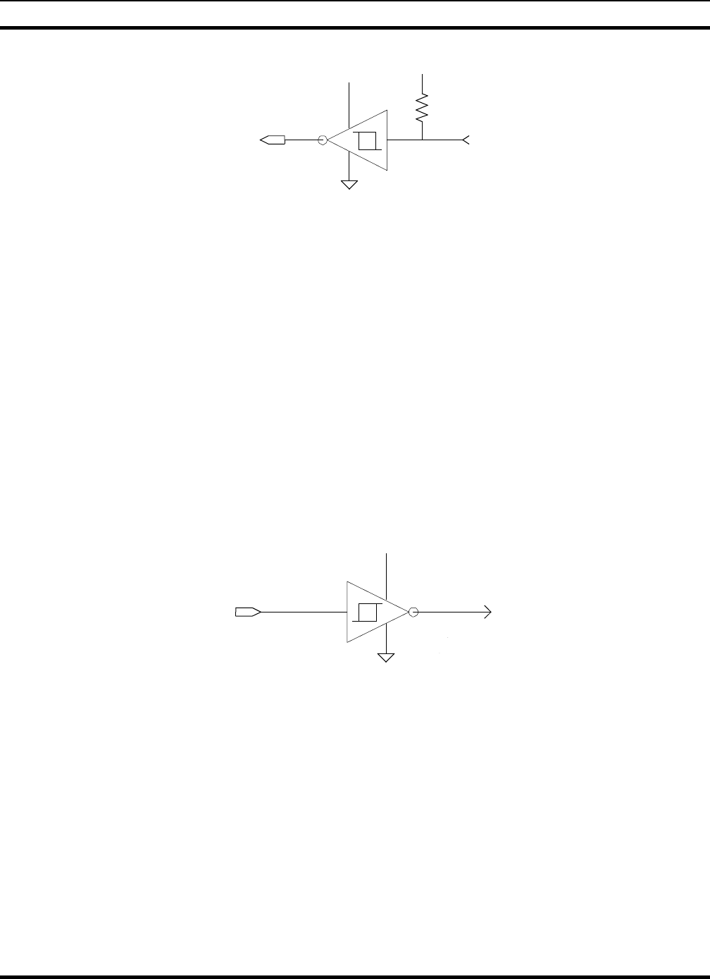
Other I/O’s are shown on Schematic Diagram WD-CB101069V1, Sheets 6 and 7. Inputs
to the microprocessor from the backplane consists of identical circuits for different
inputs. These circuits consist of inverter buffer driver circuits U18A thru F, Schmitt
Triggers U22B thru D and U23C thru F (Figure 4). Identical circuits for different inputs
also include inverter buffer driver circuits U22A thru F, U29D and U32B (Figure 5).
In Figure 4 when the input from the backplane goes low the diode is forwarded biased
and the input to the inverter goes low. This results in a sharp, well-defined output of the
inverter going high. Outputs are:
•REM-AUDIO PRESENT (U18A) •EXTADIN (U22C)
•CAS (U18B) •EXT150IN (U22D)
•CGMON (U18C) •RCVING-FROM-AV (U23C)
•LSDIN (U18D) •SYNTH-LOCK DET (U23D)
•PAFAIL (U18E) •SIMULCAST-INHBIT (U23E)
•FSLIN (U18F) •BYPASS (U23F)
•EXTPTTIN (U22B) •
MICROPROCESSOR
BACKPLANE
5.0V 5.0V
BAV99
Figure 4 - Input Circuits U18A thru F, U22B thru D and U23A thru F
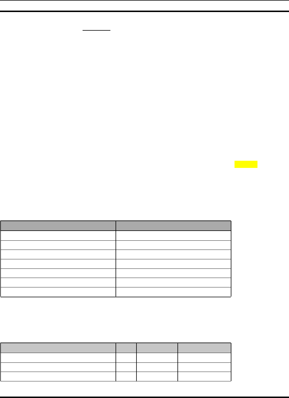
In Figure 5 the Schmitt Trigger provides a sharp, well-defined input to the
microprocessor
MM101271V1 R1A 33
CIRCUIT ANALYSISN
MICROPROCESSOR BACKPLANE
5.0V 5.0V
Figure 5 - Input Circuits U22A thru F, U29D and U32B
The FSL output from the microprocessor to the backplane is accomplished through
inverter circuit U33A and FET Q2 (BKP-FSL).
The RX-MUTE output from the microprocessor to the backplane is accomplished
through Inverter U33D and transistor circuit Q1 (BKP-RX_MUTE).
The EMSQTOAV output from the micropressor to the backplaned is accomplished
through InverterU35C and transistor circuit Q6 (BKP-EMSQTOAV).
Other outputs from the microprocessor to the backplane are connected through identical
circuits as shown in Figures 6 & 7. Figure 6 shows circuits using Schmitt Triggers U29B,
C, E, F and U32A & C to provide sharp, well-defined outputs to the backplane. Theses
outputs are:
•BKP-WALSH1 (U29B) •BKP-RFTXDAT (U29F)
•BKP-WALSH2 (U29C) •BKP-RFTXCLK (U32A)
•BKP-A/DMODCTL (U29E) •BKP-LSDOUT (U32C)
MICROPROCESSOR BACKPLANE
5.0V
Figure 6 - Output Circuits U29B, C, E & F, U33C, E & F and U34A thru F
Figure 7 shows circuits using open collector inverters circuits U33B, C, E, F, U34A, B,
C, D, E, F and U35C, D, E & F. These outputs are:
•BKP-SYNTH_DATA (U33B) •BKP- (U34D)
•BKP-SYNTH_DATA_CLK (U33C) •BKP- (U34E)
•BKP-RPTKEY (U33E) •BKP- (U34F)
•BKP-SPARE2 (U33F) •BKP- (U35C)
•BKP-CPTTOUT (U34A) •BKP- (U35D)
•BKP-SPARE1 (U34B) •BKP- (U35E)
•BKP-STNPTT (U34C) •BKP- (U35F)
34 MM101271V1 R1A

CIRCUIT ANALYSIS
MICROPROCESSOR BACKPLANE
5.0V
Figure 7 - Output Circuits U33B, C, E, F, U34A, B, C, D, E, F and U35C, D, E & F
MM101271V1 R1A 35
CIRCUIT ANALYSIS
6.3.4CPU
The Central Processing Unit (CPU) circuits for the Controller Board are shown on
Schematic Diagram WD-CB101069V1, Sheets 8 & 9 and include:
•Microprocessor •Microprocessor Support
6.3.4.1 Microprocessor
Microprocessor U9A is a Motorola MPC860P processor that has four SCC channels, two
SMC channels, plus a 100 Mbit Fast Ethernet Controller. One of the SCC channels is
used as a second ethernet port (10 Mbit) with all other SCC and AMC channels used as
serial ports.
This microprocessor runs at 59 MHz using a 29.4912 MHz clock input. This frequency
was selected for use by the baud rate generators to produce standard baud rates up to
115.2 kbaud without error. The microprocessor external bus runs at half the speed of the
microprocessor (29.5 MHz).
The microprocessor provides a real-time clock that is used to provide time-of-day
information to the application software. The real time clock runs off of a 32.768 kHz
crystal and is provided with 3.0 Volt battery voltage via the KAPWR pin of the
microprocessor to keep time when power is off.
Four external interrupts are used in this design. The remaining unused three connect to
the EPLD for future use. Connecting them to the EPLD makes later modifications easier.
The external interrupt signals are specified in the following table.
Table 4 - External Processor Interrupt Signals
Device IRQ
(SPARE-EPLD) IRQ (NMI)
QUART IRQ1
MODEM DB DUAL-PORT RAM IRQ2
(SPARE-EPLD) IRQ3
ETHERNET 10/100 IRQ4
ETHERNET 10 IRQ5
(SPARE-EPLD) IRQ6
All but one chip select are used in this design. The unused chip select is connected to the
EPLD for future use. The microprocessor chip select signals are defined in the following
table.
Table 5 - External Processor Interrupt Signals
Device IRQ Machine Data Bus Width
FLASH CS0 GPCM 32 Bit
SDRAM CS1 UPMA 32 Bit
QUART REGISTERS CS2 GPCM 8 Bit
MM101271V1 R1A 36

CIRCUIT ANALYSIS
Device IRQ Machine Data Bus Width
QUART INTERRUPT VECTOR CS3 GPCM 8 Bits
EPLD CS4 GPCM 8 Bits
MODEM DB DUAL PORT RAM CS5 UPMB58 Bits
MODEM DB CODE RAM CS6 GPCM 8 Bits
(SPARE-EPLD) CS7 N/A N/A
Note that there is both a 32-bit data bus and an 8-bit data bus. The 8-bit data bus is
connected to the 32-bit processor data bus via an 8-bit transceiver. The output enable for
the transceiver is controlled by ANDing all 8-bits chips selects together inside the EPLD.
6.4.2 Microprocessor Support
The microprocessor support as shown on Schematic Diagram WP-CB101069V1, Sheet 9
includes:
•BDM Debug Port Connector •Silicon Serial Number
•Power-On Reset Configuration •KAPWR Switch
•32 kHz Crystal •8-Bit Bus Transceiver
•VDDSYN Filter •MICTOR Logic Analyzer Connectors
BDM Debug Port Connector
For support, microprocessor U9A provides a dedicated serial port (BDM) for connecting
a debugger/emulator. A debugger/emulator connected to this port allows a programmer
to read/write registers and external peripherals, control program execution, etc. Many
debuggers also have built-in capability to program on-board flash through this port.
These serial port pins are brought to 10-pin header J1 using the standard BDM pinout
Power-ON Reset Configuration
The Power-On Reset Configuration consists of four octal buffer/drivers U6A, U6B, U8A
and U8B with 3-state outputs. This circuit ensures that at Power-On all circuits are reset
to the starting state. Inputs to these circuits are through 10K BUS8 resistor networks
RN7 and RN10. The outputs tie into bus D[0.31]. Each package is organized as two 4-bit
line drivers with separate output-enable (OE) inputs. These inputs are tied together and
connect to RESET-N. When RESET-N is low, data passes from A inputs to Y outputs.
When RESET-N is high, the outputs are in the high-impedance state.
32 kHz Crystal
This crystal circuit consist of crystal package Y3, resistors R90 and R98, capacitors C49
and C63. This circuits connects to U9A between pins N1 (EXTAL) and P1 (XTAL) and
produces an oscillator frequency of 32.768kHz to drive the real-time clock.
5 UPMB is only required if the system makes use of the BUSY_N signal coming from the dual port memory. If BUSY_N is
not used, then a GPCM machine can be used for this chip select.
MM101271V1 R1A 37

CIRCUIT ANALYSISN
29 MHz Clock
The 29 MHz Clock consists of oscillator circuit Y2 and resistors R82 and R105. This
circuit produces the oscillator frequency of 29.4912 MHz and connects to U9A at N2
(EXTCLK).
VDDSYNC Filter
This circuit consists of inductor L1 and capacitors C50 and C57. It connects between the
3.3V supply and the VDDSYN connection through capacitor C68 to microprocessor
U9A, Pin T2 XFC. The primary purpose of this circuit is to
Silicon Serial Number
A unique 64-bit electronic Serial Number chip U3 is used to store the board
identification number. This chip has a 1-bit serial port, which interfaces to
microprocessor U9A through an I/O port. In addition, four bits of hardware identification
are made available to U9A through I/O ports. The Hardware ID is changed based by
selectively populating a bank of resistors.
KAPWR Switch
The KAPWR switch consist of Schottky diodes D30 and D31 and battery BT1. This
switch applies 3.3V supply or 3.3V battery to U9A, Pin KAPWR
8-Bit Bus Transceiver
This circuit consists of 8-Bit Bus Transceiver U19 and resistor network RN15. The 8-Bit
Bus connects to the microprocessor through 8-Bit Bus Transceiver U19. The output
enable OE for the transcreiver is controlled by ANDing all 8-bit chip selects together
inside EPLD U27.
MICTOR Logic Analyzer Connectors
These connections consists of J3, J5 and J6.
6.3.5Modem Daughter Board Connector
The Modem Daughter Board connector circuits for the Controller Board is shown on
Schematic Diagram WD-CB101069V1, Sheet 10 and include:
•QUICC Connector (J1) •I/O Connector (J2)
6.5.1 QUIC Connector (J1)
The QUICC (J9) connector contains the microprocessor interface (Refer to the Modem
Daughter Board Section).
38 MM101271V1 R1A
CIRCUIT ANALYSIS
6.5.2 I/O Connector (J2)
The I/O (J2) connector has miscellaneous I/O to/from the EPLD or Interconnect Board
(Refer to the Modem Daughter Board Section).
6.4.5Electrically Programmable Logic Device (EPLD)
The EPLD circuit for the Controller Board is shown on Schematic Diagram WD-
CB101069V1, Sheet 11.
Access to various board inputs/outputs is made available through Electronically
Programmable Logic Device (EPLD) U27. The EPLD contains numerous read/write
latches with a simple 8-bit interface to the microprocessor.
The EPLD is in-circuit programmable via the JTAG port using an Altera byte-blaster
cable. A 10-Pin header is made available for this purpose. The EPLD JTAG port is also
brought to microprocessor I/O pins to allow the microprocessor to load the EPLD
configuration.
In addition to being an interface to the discrete I/O, the EPLD also divides clocks and
provides the output enable logic for the 8-bit data bus transceiver.
6.7 Ethernet Ports
There are two Ethernet Port circuits for the Controller Board and they are shown on
Schematic Diagram WD-CB101069V1, Sheets 12 & 13 as:
•10 Base-T (10 Mbit PHY) •10/100 Base-T (10/100 Mbit PHY)
The 10/100 Mbit port (10/100 Base-T Transceiver U5) uses the Fast Ethernet Controller
inside the microprocessor and supports full duplex (10/100 Base-T). The 10 Mbit port
(10 Base-T Transceiver U12) uses SCC1 and only supports half-duplex (10 Base-T). The
ethernet physical layer transceivers are the same for both ports, but the 10/100 Mbit port
uses the MASTR II interface whereas the 10 Mbit uses a “7-wire” interface. The ethernet
transceivers support 10/100 Base-T with full auto-negotiation capability, while the 10
Mbit port only advertises 10 Mbit capability.
The RJ-45 ethernet connectors are actually located on Interconnect Board A1
(Interconnect Board). The ethernet physical layer chips and transformers reside on the
Controller Board with the ethernet differential RX/TX signals brought to the RJ-45
connectors through the Interconnect Board connector. A single LINK OK status LED is
provided for each ethernet port on the front of the Controller Board.
The 10Mbit Ethernet port uses the “7-wire” interface to connect the Ethernet physical
transceiver to the microprocessor SCC1 serial channel. When SCC1 is in Ethernet mode,
the SCC pins have different functions (refer to the following table).
Table 6 - 10 Mbit Ethernet Connections
SCC Ethernet Signal SCC Pin Name PHY Signal
TX TXD1 10TXD
TENA RTS1 10TXEN
MM101271V1 R1A 39
CIRCUIT ANALYSISN
TCLK CLKx 10TXCLK
CLSN CTS1 10COL
RENA CD1 10CRS
RX RXD1 10RXD
TCLK CLKx 10RXCLK
In order to use both the SCC1 in Ethernet mode and I2C bus, the board software applies a
small microcode patch at startup. This relocates the affected overlapped registers. Make
sure to use the new register addresses in the code. To obtain the patch, go to:
http://www.mot.com/SPS/ADC/pps/subpgs/etoolbox/8XXX/i2C_spi.html.
6.4.6I2
C Bus
The I2C-bus is a two-wire serial bus (SCL and SDA) used for microcontroller-based
control. The I2C Bus circuits for the Controller Board are shown on Schematic Diagram
WD-CB101069V1, Sheet 14. These circuits consist of Personality EEPROM U14, and 8-
bit I/O expanders for the I2C bus U15 and U26.
32k of non-volatile data storage is provided by EEPROM U14. EEPROM U14 is
organized as 32kx8 and is accessible via the I2C port of microprocessor U9A.
Serial EEPROM U14 has a write protect pin. It is active high and has an external pull-up
to always make it active. To write to U14, port PB23 on the microprocessor is defined as
an output and driven low. To write protect the EEPROM after writing to it, port PB23 is
defined as an input and the pull-up activates the write protect signal.
Several peripherals are available to the microprocessor through the I2C Bus. In addition
to a 32kbyte EEPROM, there is an 8-bit writable latch for driving 4 LED’s and an 8-bit
readable latch for reading the status of an 8-bit DIP switch. The I2C bus is also brought to
the Interconnect Board for accessing other off-board peripherals (i.e. LED display). I2C
bus addresses are as follows:
Table 7 - I2C Bus Addresses
Device Addresses
LED’s 0x40
DIP Switch 0x46
EEPROM 0xA0
Digital Pot 0x50
ADC/DAC 0x9E
16-Bit Expander 0x4C
Display 0x4A
6.4.7Memory
The Memory circuits for the Controller Board are shown on Schematic Diagram WD-
CB101069V1, Sheets 15 & 16 and include:
40 MM101271V1 R1A

CIRCUIT ANALYSIS
•DRAM Circuits U2 & U7 •Flash Circuits U10 & U11
6.9.1 DRAM
Two 128-Mbit, 16 bit wide synchronous DRAM Integrated Circuit modules U2 and U7
are organized in a 4M x 32 configuration. These two modules provide a minimum of 16
Mbytes of storage, upgradeable to 64 Mbytes. The following table shows the MPC860P
bank addresses for the different DRAM memory sizes.
Table 8 - DRAM Bank Memory Ranges
Bank 64-Mbit (DRAM) 128-Mbit (2xDRAM) 256-Mbit (SDRAM)
Bank 1 0x003FFFFF – 0x00000000 0x003FFFFF – 0x00000000
0x013FFFFF – 0x01000000 0x003FFFFF – 0x00000000
0x013FFFFF – 0x01000000
0x023FFFFF – 0x02000000
0x033FFFFF – 0x03000000
Bank 2 0x007FFFFF – 0x00400000 0x007FFFFF – 0x00400000
0x017FFFFF – 0x01400000 0x007FFFFF – 0x00400000
0x017FFFFF – 0x01400000
0x027FFFFF – 0x02400000
0x037FFFFF – 0x03400000
Bank 3 0x00BFFFFF – 0x00800000 0x00BFFFFF – 0x00800000
0x01BFFFFF – 0x01800000 0x00BFFFFF – 0x00800000
0x01BFFFFF – 0x01800000
0x02BFFFFF – 0x02800000
0x03BFFFFF – 0x03800000
Bank 4 0x00FFFFFF – 0x00C00000 0x00FFFFFF – 0x00C00000
0x01FFFFFF – 0x01C00000 0x00FFFFFF – 0x00C00000
0x01FFFFFF – 0x01C00000
0x02FFFFFF – 0x02C00000
0x03FFFFFF – 0x03C00000
6.9.2 FLASH
Two flash memory modules U10 and U11 are organized as 1M x 32 for non-volatile
program storage (Flash). These two modules have 4 Mbytes of flash memory with the
ability of expansion up to 8 Mbytes. The program execution takes place directly from
flash so that performance is as important as is the ability to load new code while in the
lab and while in the field.
6.9.3 Quad UART
The QUART circuit for the Controller Board is shown on Schematic Diagram WD-
CB101069V1, Sheet 17.
Universal Asynchronous Receiver-Transmitter (UART) U28 is used to handle
asynchronous serial data communication. Asynchronous means that the data is not
synchronous, that is, it is not occurring at a steady constant rate, but is being transmitted
intermittently through serial ports. In data transmission, serial means, transmitting one
bit at a time.
The serial port is a general-purpose interface that conforms to the Recommended
Standard–232C (RS-232C) and can be used to interface with almost any type of device
(modem, mouse and serial printer, etc.).
MM101271V1 R1A 41

CIRCUIT ANALYSISN
Quad UART (U28) is accessible to microprocessor U9A for four additional serial ports.
QUART U28 runs off 3.3 volts, forcing the microprocessor interface to be asynchronous
and run at 14.75 MHz, the microprocessor bus clock divided by 2 inside the EPLD. The
communication clock input will be 3.6864 MHz, the microprocessor bus clock divided
by 8 inside the EPLD. None of the I/O ports of the QUART will be used, but the ports
are connected to mod points in case of a later use.
The QUART uses two chip selects, CS2 and CS3. Chip select CS2 is used when
accessing the QUART registers. Chip select CS3 is used after an interrupt to read the
interrupt vector.
6.5 MODEM DAUGHTER BOARD
The Modem Daughter Board contains three synchronous serial ports (modems) and a
local microprocessor. This board plugs into the Controller Board using two connectors,
QUICC (J9) and I/O (J2). Refer to Figure 4 – Modem Daughter Board Block
Diagram.
The microprocessor interface is a simple 8-bit asynchronous port with two separate chip
selects. One chip select controls access to an 8k x 8 dual port RAM. The other chip
select controls access to the Modem Daughter Board microprocessor local memory. The
Controller Board microprocessor loads the Modem Daughter Board local memory with
code before releasing the Modem Daughter Board reset. The Modem Daughter Board
microprocessor runs from a 14.7 MHz clock generated by dividing down the 29.5 MHz
Controller Board microprocessor output clock inside the EPLD.
Circuits for the Modem Daughter Board are shown on Schematic Diagram WD-
CB101074V1, Sheet 1. The Outline Diagram is shown on PS-CB101074V1.
Modem Daughter Board CB101074V1 mounts on the Controller Board and exists
primarily to support Modem chips, U9, U10, and U11. These modems process 9600 baud
serial synchronous receive and transmit data from the RF path (U9), the Phone Line
(PL) path (U10) and the Voted Digital Interconnect (VDI) path (U11).
Microprocessor U1, a Dallas 80C323, controls the three modem chips, generates the
transmit data, and processes the receive data for use by the system.
The microprocessor communicates with the QUICC processor on the Controller Board
via Dual Port RAM U3.
There is no non-volatile memory on the Modem Daughter Board. Code is loaded into
Code RAM (U2) via an interface from the QUICC processor.
Most of the circuitry on the Modem Daughter Board operates from a 3.3V supply. The
Modem chips, however, require 5V. Thus a 3.3V to 5V conversion (U6) is needed for all
signals to the Modem chips.
42 MM101271V1 R1A
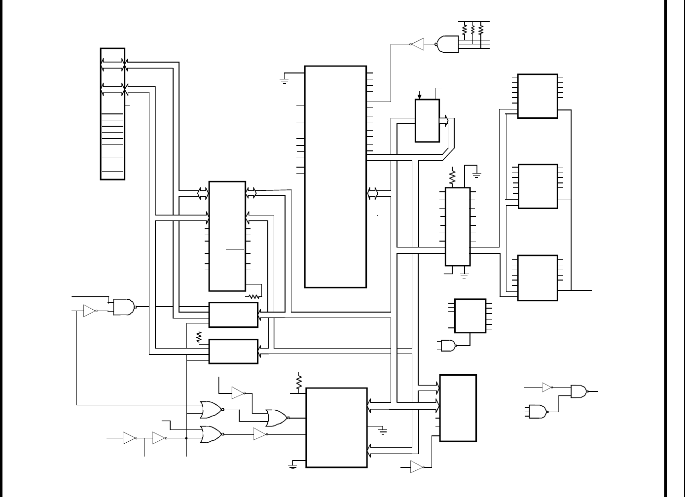
CIRCUIT ANALYSIS
QD0 - QD7
QA0 - QA15
D0 - D7
A0 - A12
QUICC
IFC
J1 U3
DUAL
PORT RAM
U1
80C323
A0 - A7
A8 - A15
U7
8-BIT
LATCH
A0 - A15
D0 - D7
U2
CODE
SRAM
64k x 8
A0 - A15 A0
A14
D0
D7
U4
SRAM
32k x 8
U6
CONV
U9
RF
MODEM
U10
PL
MODEM
U11
VDI
MODEM
U13
DATA
BUFFER (8)
U12
ADDER
BUFFER (16)
A0 - A15
D0 - D7
A0 - A7
A0 - A7
VDIMODCS/
U5
ADDRESS
DECODER
2
1
0
E
5
4
3
2
1
0
A15
A14
A13
DPRCS/
PLMODCS/
RFMODCS/
RD/
WR/
X1
X1
X1
A/D0-7
A/D0-7
A/D0-7
RFRXDAT
RFTXDAT
RFTXCLK
RFRCVDAT
RFRCVCLK
RFCS.5
ALE5 CS/
ALE
RD5
WR5
RESET5
RFINT
RD/
WR/
RESIN
INT/
RFMODCS/
PLMODCS/
UDIMODCS/
DATADIR
RD/
RESET E
DIR OE
D0-D7
A0-A7
RFCS_5
PLCS_5
VDICS_5
ALE_5
RD/_5
WR/_5
RESETS
RFMODCS/
PLMODCS/
ALE
RD/
WR/
RESET
VDIMODCS/
DATADIR
OEDIR
3.3V
LE
RESETALE
U5
3.3V
RFINT/
PLINT/
VDIINT/
RXD0
TXD0
RSD1
TXD1
INT0/
INT/R
RWINT/
PLINT/
RD/
WR/
ALE
PSEN/
EA
X114.746 MHz
RESET RESET
RESETRESET
RESETIN/
PSEN/
PSEN/
OE
DIR
D0 - D7
3.3V
R/W/L
CODECS/
CODE-A16
CODECS/QCODECS/
QRD/ DEL/
QDPRCS/ CEL/
QWR/ R/W/L
MODINT2NUC INTL/
BSY/ BUSYL/
14.756MHz 14.756MHz
RESET2MOD RESETIN/
RD/OEL/ OEL OER
CEL/ CEL CER DFRCS/
R/WL/ R/WRR/WL WR/
BUSYL/
SEML SEMR
INTL/ INTL# INTR INT/R
BUSYR
3.3V
M/S
DIR
OE
OE/
3.3 V
CODE-A16
A16
A0 - A15
RD/ OE/
SC/
WE/WR/
A15
0 PE.4
0 PE.5
0 P1.1
0 P1.4
0 P1.6
1 P1.0
P3.0
P3.1
P3.2
P3.3
P3.2 INT0/
P3.3 INT1/
P1.5 INT3/
P1.7 INT5/
P3.7
P3.6
11 MHz
MM101271V1 R1A 43

CIRCUIT ANALYSISN
Figure 8 - Modem Daughter Board Block Diagram
44 MM101271V1 R1A

CIRCUIT ANALYSIS
6.1 Modems
Each Modem chip interfaces to the 80C323 microprocessor via an 8-bit bi-directional
address/data bus, and Chip Select (CS/), Read (RD/), Write (WR/), ALE, and Interrupt
(INT/) signals.
During transmit, the microprocessor writes data to the Modem as requested by the
Modem interrupt. The Modem converts the data to a 9600 baud synchronous serial data
stream.
During receive, the Modem chip receives the 9600 baud synchronous serial data stream
and interrupts the 80C323 microprocessor whenever it has a complete byte to transfer.
The modem must also acquire bit sync and word sync from the data stream.
6.2 3.3V/5V Interface
Because the Modems require a 5V supply, and the microprocessor is on a 3.3V supply, it
is necessary to convert the voltage of signals passing between them. This is done by U6,
an IDT74FCT164245 3.3V/5V converter. Both output enable and direction can be
controlled for the two 8-bit sections of this IC.
In this case, the outputs are always enabled, so the OE/ pins are tied low. Section 1 is
used for signals, which only go from the microprocessor to the Modems, so Pin 1 (1DIR)
is tied high. Section 2 is used for the bi-directional bus. Pin 24 (2DIR) is driven by logic
which sets the direction from microprocessor to Modems (high) most of the time. Only
during a read of one of the microprocessors is the direction reversed (low).
6.3 Microprocessor
The 80C323 microprocessor is a 3.3V version of the Dallas Speedy micro, an 80C32
derivative. It operates on a 14.7462 MHz. Clock, which is convenient for generating
standard baud rates. It interfaces with the Modems, Code RAM, Dual Port RAM, and
Data RAM via standard address and data busses.
The microprocessor has 2 asynchronous serial ports (TXD0/RXD0 and TXD1/RXD1)
which may be used in the SitePro system for diagnostics. Both ports are available on the
rear of the SitePro shelf.
Six bits of 80C323 microprocessor I/O are used in a SitePro configuration. WALCLK,
WAL1, WAL2, and HSACQCTL are outputs, while LSRX and MODFSL are inputs.
The microprocessor has only two level sensitive interrupts, INT0/ and INT1/. The first,
INT0/, is used for all Modem interrupts. The second, INT1/, is used for interrupts from
the Dual Port Ram.
Since it is still necessary to distinguish between the three Modem interrupts, RFINT/ and
PLINT/ are brought to I/O pins so the microprocessor can easily determine which
Modem is interrupting. i.e. If a Modem interrupt occurs, the microprocessor looks at the
two pins. If either or both are low, the corresponding interrupts are serviced. If neither is
low, the VDI interrupt is serviced.
The 80C323 (U1) uses standard Intel multiplexed address/data bussing. During the first
half of the bus cycle, U7 latches the lower 8 bits of address under the control of ALE.
MM101271V1 R1A 45
CIRCUIT ANALYSISN
Address decoder U5 generates the Chip Selects for the three modems and the Dual Port
RAM using signals RD/, WR/, A13, A14, and A15.
Table 9 - Memory Map
MEMORY MAP
Device Range Size
Code RAM 0-FFFF 64K
Bytes
Dual Port RAM 0-1FFF 8K Bytes
Data RAM 8000-FFFF 32K
Bytes
RF Modem 2000-2003 4 Bytes
PL Modem 4000-4003 4 Bytes
VDI Modem 6000-6003 4 Bytes
6.4 Code Memory
Code is stored in 128K byte RAM U2. The microprocessor can then access it via the
Address and Data bus using PSEN/.
Code is loaded into U2 from the QUICC microprocessor. During loading, the QUICC
holds the 80C323 reset with the RESETIN/ (low) signal. This is required so the 80C323
will not try to access U2 at the same time causing bus contentions. During loading, bus
transceivers U12 (address bus) and U13 (data bus) are turned on. They are held inactive
at all other times by the same RESETIN/ signal.
The QUICC controls Code memory access through signals RESETIN/, R/WL, CODECS/
and CODE_A16. While RESETIN/ is held low, the QUICC can write or read U2.
CODE_A16 can be used to control which 64K byte half of U2 is used. Thus, for
instance, Control Channel code could be stored in one half and working channel code in
the other. The switch is performed while the 80C323 is held reset, so it is entirely
transparent to the 80C32.
When RESETIN/ is high, the bus transceivers U12 and U13 are off and the 80C323
controls the bus.
6.5 Data Memory
Data is stored in 128K byte RAM U4, however, only 32K is used. Chip select is A15/,
thus the RAM is addressed in the upper half of memory space.
6.6 Dual Port Ram
Dual Port RAM U3, an IDT70V05 8K byte device, is the communication path between
QUICC and 80C323 during normal operation. Either microprocessor can read or write
any location in the RAM. Protocols must be established in software to avoid contention.
The QUICC can interrupt the 80C323 by writing to Address ______. This causes
interrupt line INTR/ to go low. It is cleared by a read of the same address by the 80C323.
Likewise, the 80C323 can interrupt the QUICC by writing to address ____, which causes
a QUICC interrupt on line INTL/.
46 MM101271V1 R1A

CIRCUIT ANALYSIS
The 80C323 accesses the DPR via its address and data busses using signals DPRCS/,
RD/, WR/, and INTl/.
The QUICC accesses the DPR via its address and data busses using corresponding
signals CEL/, R/WL/, OEL/, and INTL/.
6.7 Troubleshooting Aids
Several signals are available on diagnostic connector J3 for troubleshooting purposes.
Also probe points are provided for GND, 5V, and 3.3V.
MM101271V1 R1A 47

CIRCUIT ANALYSIS
6.4ROCKWELL MODEM INTERFACE CARD (A3)
7.0 QIUCC Connector
6.2 Dual Port RAM
6.3 Microcontroller
6.4 8-bit Latch
6.5 Address Buffer
6.6 Data Buffer
6.7 Code SRAM
6.8 Data SRAM
6.9 Page Connections
6.10 Address Decoder
6.11 Diagnostic Connector
6.12 3/5 Converter
MM101271V1 R1A 48

CIRCUIT ANALYSIS
6.13 I/O Connector
6.14 RF Modem
6.15 PL Modem
Phone Line Modem
6.16 VDI Modem
Voted Digital Interface Modem
MM101271V1 R1A 49

CIRCUIT ANALYSIS
6.4 ANALOG BOARD (A4)
Analog Board CV101070V1 contains programmable high speed filters, low speed
encode and high speed decode. This board includes Simulcast Interface hardware, which
eliminates the need for the older Simulcast Interface Board in Simulcast applications.
Refer to Outline Diagram PS-CB101070V1 and Schematic Diagram WD-CB101070V1.
6.5.1Quad ADC and Single DAC
AD/DA Converter U23 is an 8-bit CMOS data acquisition device with four analog
inputs, one analog output and a serial I2C-bus interface. Three address pins A0 (Pin 5),
A1 (Pin 6) and A2 (Pin 7) can be used for programming a hardware address, allowing the
use of up to eight devices to be connected to the I2C-bus without additional hardware. In
this application, these three leads are tied to +5V. Address, control and data to and from
the device are transferred serially through the two-line bidirectional I2C-Bus. The PWR
SENSE lead is connected to analog input AIN0 at U23, Pin 1, converted to digital and
connected to the I2C-bus.
6.5.28-Bit I/O Expander for I2
C Bus
8-Bit I/O Expander U4 consists of a 16-bit two-line quasi-bidirectional port and an I2C-
bus interface. The two-line I2C inputs SCL and SDA connect to U4, Pins 22 and 23
respectively. These two-line inputs can be monitored at Test Points TP2 and TP3. The
expanded outputs and connections are U4, Pin:
•4 (P0) – HS-FILTERSEL0 (Monitored
at TP19) •13 (P10) - ground
•5 (P1) – HS-FILTERSEL1 (Monitored
at TP24) •14 (P11) - ground
•6 (P2) – HS-FILTERSEL2 (Monitored
at TP25) •15 (P12) - ground
•7 (P3) – HSACOCTL1 (Monitored at
TP26 •16 (P13) – ground
•8 (P4) – LSCTL (Monitored at TP30) •17 (P14) - ground
•9 (P5) - (Monitored at TP29) •18 (P15) – Connects to +5V through
voltage divider network R127, Pin 8
•10 (P6) – MODCTL (Monitored at
TP28) •19 (P16) – Connects through voltage
divider network R127, Pin 7 to Pin 5
to U4, Pin 20 (P17)
•11 (P7) – LSDATAACC (Monitored
at TP27) •20 (P17) – Connects through voltage
divider network R127, Pin 5 to Pin 7
to U4, Pin 19 (P16)
6.5.3–5 Volt Generation
-5 Volt generation is accomplished through voltage regulator U2. –12 Volts is applied to
U2, Pin 4 IN. Capacitors C3 and C4 provide filtering of this input. The output is at U2,
Pin 3 Out. The –5 Volts is filtered by capacitors C5 and C6. –5Volts can be monitored at
MM101271V1 R1A 50

CIRCUIT ANALYSIS
Test Point TP31 by connecting the negative lead to TP31 and the positive lead to ground
(TP32 or TP33).
6.5.4High-Speed Data Transmit Filters
Buffer/follower circuit U6A precludes the quad operational amplifier high-speed data
transmit filter circuits for RFTXDAT. The output of this circuit can be monitored at TP1.
The output of U6A is applied to the inputs of high-speed Data Transmit Filters:
•9600 Baud Wide Band
•4800 Baud Narrow Band
•9600 Baud Wide Band ETSI6
•4800 Baud Narrow Band ETSI
•9600 Baud Narrow Band Switched Capacitor Filter Circuit
The High Speed Data (HSD) filter is an active Gaussian Minimum Shift Keying
(GMSK) filter that filters the data transitions to minimize the high-speed-data
transmission bandwidth. The frequency response of the HSD filter section is changed by
selecting the output of only one filter circuit by 8:1 MUX U7.
High-speed data is a 4800 or 9600 bit per second data stream generated by the
microcomputer through the RF data modem U9 on the Modem Daughter Board.
Each of the HSD filter circuits has two sections.
6.5.4.1 9600 Baud Wide Band
This HSD filter circuit consists of operational amplifier U5B followed by operational
amplifier U5A. The output of U5A, Pin 1 is applied to the input of 8:1 MUX U7, Pin 4
(N01). This HSD amplifier filter output can be monitored at TP4.
6.4.4.2 4800 Baud Narrow Band
This HSD filter circuit consists of operational amplifier U5C followed by operational
amplifier U5D. The output of U5D, Pin 14 is applied to the input of 8:1 MUX U7, Pin 5
(N02). This HSD amplifier filter output can be monitored at TP5.
6.4.4.3 9600 Baud Wide Band ETSI
This HSD filter circuit consists of operational amplifier U10B followed by operational
amplifier U10A. The output of U10A, Pin 1 is applied to the input of 8:1 MUX U7, Pin 6
(N03). This HSD amplifier filter output can be monitored at TP6.
6.4.4 4800 Baud Narrow Band ETSI
This HSD filter circuit consists of operational amplifier U510C followed by operational
amplifier U10D. The output of U10D, Pin 14 is applied to the input of 8:1 MUX U7, Pin
7 (N04). This HSD amplifier filter output can be monitored at TP7.
6 European Technical Standards Institute
MM101271V1 R1A 51

CIRCUIT ANALYSISN
6.4.4 9600 Baud Narrow Band
This HSD filter circuit consists of switched-capacitor filter circuit U11 required to
produce a flat frequency response. This circuit is driven by an external 400 kHz clock on
U11, Pin 1. The output on U11, Pin 5 is applied to the input of 8:1 MUX U7, Pin 12
(N05). This HSD filter circuit output can be monitored at TP8.
6.5.68:1 MUX
Multiplexer circuit U7 is used to select the applicable HSD to be passed on to Dual
Digital Potentiometer U8. The inputs to U7 are applied to N01 through N05 (Pins 4, 5, 6,
7 and 12). The selection of HSD is made by the HS-FILTER_SEL inputs on U7, Pin 1
(A0), Pin 15 (A1) and Pin 15 (A2). EN (Enable) on Pin 2 is connected to +5V. The 8:1
MUX output COM is on U7, Pin 8.
6.5.7Dual Digital Pot
The output of the MUX circuit connects to the input of Addressable Dual Digital
Potentiometer U8, Pin 14 (HO). This device has two independently controlled
potentiometers. Only one pot is used in this application. The wiper can be set to one of
256 positions and is controlled by the microprocessor through the I2C data bus SCL (Pin
9) and SDA (Pin 10). The output on Pin 12 (WO) connects to the input of amplifier
circuit U6B.
6.5.8Inverting Buffer/Amplifier
Amplifier circuit U6B is an inverting buffer/amplifier with a gain of approximately 1.5.
The output of this circuit is connected to the input of analog switch U9. The output of
this circuit can be monitored at TP9.
6.5.9 Analog Switch
Analog Switch U9 is a Single-Pole/Double Throw (SPDT) with one normally closed and
one normally open switch. Switching times are less than 175 ns max for tON and less
than 145 ns max for tOFF. Analog Switch U9 switches between RFTXDATA (U9, Pin 2
(S1)) coming from inverting Buffer/amplifier U6B and ANALOG AUDIO (U9, Pin 8
(S2)). S1, Pin 2 (RFTXDATA) is the normally closed contacts. The output is on U9, Pin
1 (D) MOD. This device is controlled by MODCTL on U9, Pin 6 (IN). +5V connects to
U9, Pin 5, (VL). +12V connects through Diode D1 to U9, Pin 4 (+V) and –12V connects
through Diode D2 to U9, Pin 7 (-V).
6.5.8Clock Generation
Clock generation is accomplished by inverter circuits U32C and U32D and Dual 4-Stage
Binary Ripple Counter U3. U32C and 400 kHz crystal Y1 form a 400 kHz oscillator
circuit. The output of U32C connects to the input of U32D. The 400 kHz clock (CLK)
output of 32D connects to U3, Pin 1 (CP1). This 400 kHz CLK can be monitored at
TP10. Counter U3 divides the 400 kHz CLK down to produce a 25 kHz CLK. This
output can be monitored at TP11. The 400 kHz CLK is further divided down to produce
a 3.125 kHz CLK. This output can be monitored at TP12.
52 MM101271V1 R1A

CIRCUIT ANALYSIS
6.5.9Low Speed Data Decoder Filter
The Low Speed Data Decode Filter is used to remove voice-audio (300-3000 Hz) leaving
only the low-speed or subaudible data for an input to the microprocessor.
VOLSQ is coupled through capacitor C33 to the input of buffer/follower circuit U15A
6.5.10Low Speed Data Encode Filter
The Low Speed Data Encode filter is used to smooth out transitions of data impressed
upon the voice audio. Low-speed data is a 150 bit per second data stream generated by
the microcomputer and used to produce subaudible data on the voice audio.
Low-Speed Data is generated by microcomputer U9A through EPLD U27, Pins 81 and
80, Walsh Bit 1 and Walsh Bit 2 respectively. For low-speed data, the two Walsh bits are
scaled and summed through analog switch U22. The output of U22, Pin 1 (D) connects
through operational amplifier U19A and buffer/follower U19B to the input of the low-
speed-data encode filter U21. The output of U19B can be monitored at TP22. U21 is an
active filter, which uses resistors R82, R90 and R93 with an external 3.125 kHz CLK to
produce a low-pass filter. The output of U21 can be monitored at TP20. This output
connects to the input of low pass filter U20, Pin14 (IN). This filter
6.6POWER SUPPLY (A5)
MM101271V1 R1A 53

CIRCUIT ANALYSIS
6.7MISCELLANEOUS INFORMATION
6.7.1Serial Port Data Format
The serial ports transfer RS-232 asynchronous serial data at a rate of 19.2k using the
half-duplex operating mode. That is, data flows in only one direction at a time. The
characteristics of the communication link are:
Type: RS-232C
Baud Rate: 19.2 kilobaud
Start Bits: 1
Stop Bits: 1
Parity: None
Data Type: Binary
6.7.2Failsoft Data Format
Communication between SitePro’s takes place along the Backup Serial Link (BSL)
through J4. The characteristics of the communication link are:
Level: 0 to 13.8 VDC
Mark/Space: 13.8 volts (mark)/0 volts (space)
Baud Rate: 19.2 kilobaud/38.4 kilobaud (ES)
Start Bits: 1
Data Bits: 8
Stop Bits: 1
Parity: None
Data Type: Binary
SitePro’s installed in Enhanced Sites (ES) must use a data rate of 38.4K baud to
improve message throughput and alleviate any conflicts due to increased traffic.
6.7.3T1/E1 Interface
In systems using a T1/E1 interface, a T1/E1 multiplexer provides an asynchronous serial
interface between the SitePro and the IMC MIM.
6.7.4Phone Port Data Format
The SitePro sends and receives modem data from its telephone port at 9600 baud using
the full duplex mode. That is, data flows simultaneously in both directions. Refer to the
Rockwell Modem section for a detailed description.
54
MM101271V1 R1A

INSTALLATION
7.0 INSTALLATION
MM101271V1 R1A 55

CONFIGURATION
8.0 CONFIGURATION
56
MM101271V1 R1A

PROGRAMMING
9.0 PROGRAMMING
MM101271V1 R1A 57

TROUBLESHOOTING
10.0TROUBLESHOOTING
58
MM101271V1 R1A
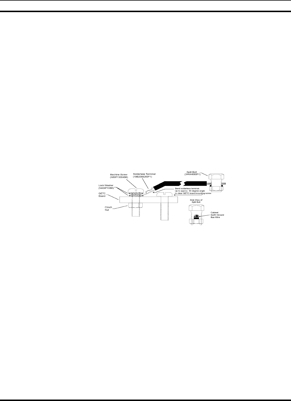
LIGHTNING PROTECTION GROUNDING
11.0LIGHTNING PROTECTION GROUNDING
Maximum lightning protection is achieved when the GETC Lingtning-Protection
Grounding Kit (344A4500) is installed. This kit is normally installed at the factory for all
trunking applications. The following procedure summarizes the installation process:
1. Two wires (black #16 AWG hookup wire, 2-feet long) are prepared as follows:
a. The wires are stripped and tinned ½-inch on one end and 1-inch on the other end.
b. A solderless terminal (19B209260P1), bent approximately 30-degrees so it will
clear the board mounting screw, is attached to the end stripped back ½-inch on
each wire as shown in Figure.
Figure 9 - Lightning-Protection Kit Installation Detail
2. The solderless terminal end of the wires is then attached to the SitePro Controller
Interconnect Board A1 using the lock washers and machine screw as shown in the
above Figure. A chinch nut is already mounted to the solder side of the board.
3. The wires are then routed out of the shelf as shown in Figure 4.
MM101271V1 R1A 59
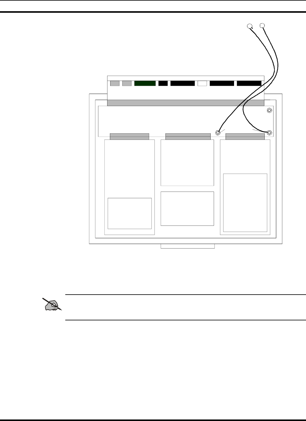
GLOSSARY
Interconnect Board
Controller Board Rockwell Modem
Interface Card
Modem Daughter
Board
Power Supply
Rockwell Modem
Assembly
Analog Board
Bolt Solderless
Terminal to Board.
Figure 10 - Lightning-Protection Kit Cabinet Installation
4. When the shelf is installed in the rack, use the split bolts to attach the wire ends
stripped 1-inch to the cabinet earth-ground bus wire (part of the Cabinet grounding
Strap Kit 344A4730) as shown in the split bolt side view in Figure 3.
NOTE
In order to be effective, the Cabinet Grounding Strap must be strapped to the building
and/or earth ground.
60 MM101271V1 R1A

INSTALLATION
12.0GLOSSARY
MM101271V1 R1A 61
PARTS LIST
13.0PARTS LIST
SITEPRO SHELF ASSEMBLY
EV101209V1
SYMBO
LPART
NUMBER DESCRIPTION
1MA101080V1 Chassis Assembly.
219A116552P3 Clamp, Cable.
3FM101081V1 Cover.
419A702381P60
8Screw, Thread Form, TORX, M4 x 8mm.
519A701312P6 Flat washer, M4.
619A702364P50
8Screw, Machine, TORX, M4X8mm.
719A700032P7 Lock washer, Internal Tooth, M4.
8FM101231V1 Spacer Plate, Shelf Door.
9FM101232V1 Lens keeper, Door.
10 AG101229V22 EMI Shielding Gasket, 22 Fingers.
11 AG101229V5 EMI Shielding Gasket, 5 Fingers.
12 AG101230V1 Lens, EMI Shielding.
13 19A700032P3 Lock washer, Internal Tooth, M2.5.
14 19A700034P3 Nut, M2.5 X 0.45.
15 NP101233V1 Rear Label.
16 FM101083V1 Support, Front.
A1 CB101073V1 INTERCONNECT BOARD
- - - - CAPACITORS - - - -
C1
and
C2
470pF, 2KV: sim to Arco
MC1808X471KN202.
- - - - JACKS - - - -
J1
thru
J3
DIN 96_ABC-P: sim to AMP 650895-4.
J4
thru
J5
RJ11_MULT: sim Stewart SS-7368H22-NF.
J6 CON10: sim to Stewart SS-7188S-A-NF.
J5 CON10: sim to Stewart SS-7188S-A-NF.
J7 19A116659P17
3CONN PWR 4-R.
J8 19A116659P10
1CONN PWR 3-P.
J9 19A116659P10
5CONN RCPT 6.
MM101271V1 R1A 62
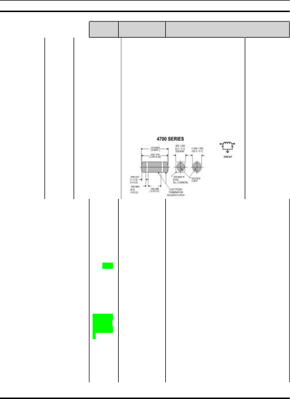
PARTS LIST
SYMBO
LPART
NUMBER DESCRIPTION
J10 19A704852P30 CONN RCPT 4.
J11 HEADER 20: sim to AMP 102160-4.
J12 CON24: sim to AMP 102160-5.
J13 HEADER 26: sim to AMP 102160-6.
J14 RJ45_MULT: sim to Stewart SS-73XXX.
- - - - RESISTORS - - - -
R1
thru
R4
REP_623_642/
75 75 Ohms, 1%, 0.63W.
- - - - Pi FILTERS - - - -
U1
thru
U29
Capacitor: 100pF, 100WVDC@125º C,
+80%/-20%: sim to Tusonix 4700 006.
A2 CB101069V1 CONTROLLER BOARD
- - - - BATTERY - - - -
BT1 Coin: 3V. 165 mAh: Sim to Panasonic Thru-
Hole.
- - - - CAPACITORS - - - -
C1 Tantalum: 1.0µF, 20V ±20%.
C2
thru
C9?
Ceramic: 0.1µF, 25V ±10%.
C10
C11
C12 Tantalum: 1.0µF, 20V ±20%.
C13
C14 Ceramic: 470pF, 2kV ±20%.
C15
thru
C30
?
C31 Ceramic: 470pF, 2kV ±20%.
C39 Tantalum: 1.0µF, 20V ±20%.
C42 Tantalum: 1.0µF, 20V ±20%.
MM101271V1 R1A 63

PARTS LISTS
SYMBO
LPART
NUMBER DESCRIPTION
C46 Tantalum: 1.0µF, 20V ±20%.
C49 Ceramic: 10pF, 100V ±10%.
C57 Tantalum: 10µF, 16V±20%.
C63 Ceramic: 10pF, 100V ±10%.
C65 Ceramic: 100pF, 100V±10%.
C66 82pF
C68 Ceramic: 820pF, 25V±10%.
C74 Tantalum: 1.0µF, 20V ±20%.
C93 Ceramic: 0.001µF, 25V ±10%.
C96
and
C97
Tantalum: 10µF, 16V±20%.
C10
6Ceramic: 0.001µF, 25V ±10%.
C11
1
Ceramic: 0.001µF, 25V ±10%.
C11
5Ceramic: 0.033µF, 25V ±10%.
C11
7Tantalum: 10µF, 16V±20%.
- - - - DIODES - - - -
D1
thru
D4
LED: Red, Thru-hole, RT ANGLE.
D5 LED: Green, Thru-hole, RT ANGLE.
64 MM101271V1 R1A
PARTS LIST
SYMBO
LPART
NUMBER DESCRIPTION
D6
and
D7
LED: Yellow, sim to Citizen 1206.
D8 LED: Green, Thru-hole, RT ANGLE.
D9
and
D10
LED: Yellow, sim to Citizen 1206.
D11 Dual, High-Speed: sim to Philips, BAV99,
SOT23.
D12 LED: Green, thru-hole
D13
thru
D17
?
Dual, High-speed: sim to Philips, BAV99,
SOT23.
D30
and
D31
Schottky, Vf=0.4
- - - - JACKS - - - -
- - - - INDUCTOR - - - -
L1 39µH ±15%.
- - - - RESISTORS - - - -
R1 19A149818P10
3Metal Film: 10k Ohms ±5%, 0.1W.
R2
thru
R4
19A149818P10
2Metal Film: 1k Ohms ±5%, 0.1W.
R5 19A149818P10
3Metal Film: 10k Ohms ±5%, 0.1W.
R6
thru
R8
0 Ohms.
R9
thru
R13
39 Ohms.
R14
and
R15
19A149818P75
0Metal Film: 75 Ohms ±5%, 0.1W.
R16
and
R17
19A149818P10
3Metal Film: 10k Ohms ±5%, 0.1W.
MM101271V1 R1A 65

PARTS LISTS
SYMBO
LPART
NUMBER DESCRIPTION
R18
R19 19A149818P22
2Metal Film: 2.2k Ohms ±5%, 0.1W.
R20 39 Ohms
R21
R22 49.9 Ohms ±1%.
R23 19A149818P33
1Metal Film: 330 Ohms ±5%, 0.1W.
R24 19A149818P15
2Metal Film: 1.5k Ohms ±5%, 0.1W.
R25 19A149818P10
2Metal Film: 1k Ohms ±5%, 0.1W.
R26
R27
R28
and
R29
19A149818P10
3Metal Film: 10k Ohms ±5%, 0.1W.
R30
R31
R32
thru
R34
49.9 Ohms ±1%.
R35 19A149818P33
1Metal Film: 330 Ohms ±5%, 0.1W.
R36
R37
R38 10k Ohms ±1%
R39
R40
and
R41
19A149818P75
0Metal Film: 75 Ohms ±5%, 0.1W.
R42 19A149818P33
1Metal Film: 330 Ohms ±5%, 0.1W.
R43 0 Ohms
R44
R45 0 Ohms
R46
R52
and
R53
49.9 Ohms ±1%.
66 MM101271V1 R1A
PARTS LIST
SYMBO
LPART
NUMBER DESCRIPTION
R54 19A149818P33
1Metal Film: 330 Ohms ±5%, 0.1W.
R55 19A149818P12
1Metal Film: 120 Ohms ±5%, 0.1W.
R56
thru
R58
19A149818P10
2Metal Film: 1k Ohms ±5%, 0.1W.
R59 19A149818P12
1Metal Film: 120 Ohms ±5%, 0.1W.
R60
R61 19A149818P12
1Metal Film: 120 Ohms ±5%, 0.1W.
R62
R63
R64
R65
R66 19A149818P12
1Metal Film: 120 Ohms ±5%, 0.1W.
R71
and
R72
19A149818P12
1Metal Film: 120 Ohms ±5%, 0.1W.
R73
and
R74
19A149818P10
5Metal Film: 1 Meg Ohm ±5%, 0.1W.
R75 3.01k Ohms ±1%.
R80 33k Ohms
R85 10.0k Ohms ±1%.
R86
R87 19A149818P33
1Metal Film: 330 Ohms ±5%, 0.1W.
R90 10 Meg Ohms ±5%, 1/16W.
R95 470k Ohms ±1%.
R98 200k Ohms
MM101271V1 R1A 67

PARTS LISTS
SYMBO
LPART
NUMBER DESCRIPTION
R11
119A149818P75
0Metal Film: 75 Ohms ±5%, 0.1W.
R13
619A149818P22
2Metal Film: 2.2k Ohms ±5%, 0.1W
R14
0and
R14
1
510
R14
2and
R14
3
Metal Film: 2.2k Ohms ±5%, 0.1W.
R14
4
R14
5510
R14
6
R14
73.9k Ohms
R14
8
R14
9100
R15
03.9k Ohms
R15
1510
R15
2
R15
30.015 Ohms ±1%, 0.5W ±1%.
R16
03.9k Ohms
R16
119A149818P10
0Metal Film: 10 Ohms ±5%, 0.1W
R16
2100
R16
75.5k Ohms ±1%, 0.1W
68 MM101271V1 R1A

PARTS LIST
SYMBO
LPART
NUMBER DESCRIPTION
R16
82.0k Ohms ±1%, 0.1W
R16
9100
R17
03.9k Ohms
R17
119A149818P47
2Metal Film: 4.7k Ohms ±5%. 0.1W.
R17
227k Ohms
R17
719A149818P47
2Metal Film: 4.7k Ohms ±5%. 0.1W.
R17
919A149818P47
2Metal Film: 4.7k Ohms ±5%. 0.1W.
R18
14.3 Meg Ohms ±5%, 1/16W.
R18
333k Ohms
- - - - RESISTOR NETWORKS - - - -
RN1
thru
RN1
5
10k Ohms, BUS8, ±5%, 0.063W.
- - - - SWITCHES - - - -
S1 PUSHBUTTON, SPST N.O./SPST N.C.
S2 DIPSWITCH, 8 position.
- - - - TEST POINTS - - - -
TP1
thru
TP1
0
SM Test Point Loop – Surface Mount: sim to
ADI/ SM-TESTPAD/Comp-CORP/TP-107/1.
- - - - TRANSFORMERS - - - -
T1
and
T2
1:1, 10/100Mbps: sim to TG110-S05N2.
- - - - TRANSISTORS - - - -
Q1 NPN: Switching: sim to Phillips PMBT3904,
SOT23.
MM101271V1 R1A 69

PARTS LISTS
SYMBO
LPART
NUMBER DESCRIPTION
Q2
thru
Q4
FET: Small-Signl, N-Channel: sim to
INFINEON, BSP295.
Q5 MOSFET: N-Channel, 5A, 20V: sim to ON
Semiconductor, MMSF5N02HD.
Q6
and
Q7
NPN: Switching: sim to Phillips PMBT3904,
SOT23.
Q8 PNP: sim to Motorola, MMBT3906LT1,
SOT23.
Q9
and
Q10
NPN: Switching: sim to Phillips PMBT3904,
SOT23.
- - - - INTEGRATED CIRCUITS - - - -
U1 Single Buffer with 3-State Output: sim to
Fairchild NC7SZ125M5, SOT23-5.
U2 8M x 16 SCRAM, PC100: sim to Micron
MT48LC8M16A2TG-8E, TSOP54.
U3 Silicon Serial Number: sim to Dallas,
DS2401P, TSOC6.
U4 Clock Buffer: sim to Cypress Cy2305SC-1,
SOIC8.
U5 10/100-TX/FX Ethernet Transceiver: sim to
AMD AM79C874VC, TQFP80.
U6 Octal Buffer, 3.3V: sim to TI 74LVC244ADB,
SSOP20.
U7 8M x 16 SCRAM, PC100: sim to Micron
MT48LC8M16A2TG-8E, TSOP54.
U8 Octal Buffer, 3.3V: sim to TI 74LVC244ADB,
SSOP20.
U9 Microprocessor, 66MHz: sim to Motorola,
XPC860PZP66D4, BGA357.
U10
and
U11
1M x 16/2M x 8 Flash, simultaneous
Read/Write: sim to AMD,
AM29DL163DB90E1, TSOP48.
U12 10/100-TX/FX Ethernet Transceiver: sim to
AMD AM79C874VC, TQFP80.
U13 RS232 Transceiver, 5V, 2-TX, 2-RX: sim to
MAXIM, MAX202CSE, SOIC16..
U14 EEPROM, I2C, 16k x 8, 3.3V: sim to Atmel,
AT24C128, SOIC8.
U15 I2C Bus 8-bit I/O: sim to Philips, PCF8574T,
SOIC16.
U16 Phase-Lock-Loop (PLL): sim to TI,
74HCT4046ADB, SSOP20.
70 MM101271V1 R1A

PARTS LIST
SYMBO
LPART
NUMBER DESCRIPTION
U17 Single Inverter: sim to Philips,
74HC1G04GW, SOT-353.
U18 HEX Buffer: sim to Philips, 74HC14PW,
TSSOP14.
U19 Octal XCVR, BUS HOLD, 3.3V, sim to Philips,
74LVCH245APW, TSSOP20.
U20 Single Inverter: sim to Philips,
74HC1G04GW, SOT-353.
U21 RS485 Transceiver: sim to TI, 75176BD,
SO8.
U22
and
U23
HEX Buffer: sim to Philips, 74HC14PW,
TSSOP14.
U24 RS232 Transceiver, 3V to 5.5V, 3-TX, 5-RX:
sim to MAXIM, MAX3241CAI, SSOP28.
U25 +5V Regulator, 1.5A: sim to Linear Tech,
LT1086CM-3.3, TO263.
U26 I2C Bus 8-bit I/O: sim to Philips, PCF8574T,
SOIC16.
U27 144 PIN CPLD, sim to Altera,
EPM3256ATC144, TQFP144.
U28 Quad UART (QUART): sim to
SC28L194A1BE, TQFP80.
U29 HEX Buffer: sim to Philips, 74HCT14PW,
TSSOP14.
U30 RS232 Transceiver, 5V, 4-TX, 5-RX: sim to
MAXIM, MAX213CAI, SSOP28.
U31 Reset Supervisor: sim to Dallas, DS1818R-
10, SOT23.
U32 HEX Buffer: sim to Philips, 74HCT14PW,
TSSOP14.
U33
thru
U35
HEX Open-Collector Output Drivers: sim to
Philips, 7406AD, SOIC14.
U36 RS232 Transceiver, 3V to 5.5V, 5-TX, 3-RX:
sim to MAXIM, MAX3237CAI, SSOP28.
U37 Hot Swap Controller: sim to Linear Tech,
LTC1422, SOCI8.
U38 Single 2-Input NAND Gate: sim to Phillips,
74AHC1G00GW, SOT353.
U39 HEX Open-Collector Output Drivers: sim to
Philips, 74F06AD, SOIC14.
U40 555 Timer: sim to National, LMC555CM,
TO263.
- - - - OSCILLATORS - - - -
MM101271V1 R1A 71

PARTS LISTS
SYMBO
LPART
NUMBER DESCRIPTION
Y1 Crystal: 25MHz CLK ±50ppm, 40%/60% duty,
3.3V
Y2 Crystal: 29,4912 MHz CLK ±100ppm,
40%/60% duty, 3.3V.
Y3 Crystal: 32.786kHz CLK
Y4 Crystal: 11.0592 MHz CLK ±50ppm,
40%/60% duty, 3.3V.
A3 ROA 117
2247/1 ROCKWELL MODEM INTERFACE CARD
- - - - CAPACITORS - - - -
C1
thru
C4
RJE 584
3168/47 Tantalum: 47µF ±20%, 16V.
C6 RJC 464
3045/1 10nF ±10%, 50V.
C7 RJA 528
4064/1 1nF, ± 5%, 16V.
C8 RJE 584
3168/47 Tantalum: 47µF 20%, 16V.
C9 RJE 584
3108/1 Tantalum: 10uF 20%, 10V.
C10
thru
C15
RJC 464
3045/1 10nF ±10%. 50V.
- - - - FUSE - - - -
F1 NGH 241 04/1 Glass-Tube: 1.0 A
F2
and
F3
NGH 241 03/25 Glass-Tube: 0.25A
- - - - RESISTORS - - - -
R1
and
R2
REP 645
623/62 620 Ohms ±1%, 0.25W
R3 REP 645
623/22 220ohm 1% 0.25W
R4
and
R5
REP 625
426/33 Chip: 330k Ohms 5%, 1/8W.
R6
thru
R17
REP 625 425/1 Chip: 10k Ohms 5%, 1/8W.
R18
thru
R21
REP 625
424/47 Chip: 4.7k Ohms 5%, 1/8W.
72 MM101271V1 R1A

PARTS LIST
SYMBO
LPART
NUMBER DESCRIPTION
R22
thru
R27
REP 625 424/1 Chip: 1k Ohms 5%, 1/8W.
R28 REP 625 425/1 Chip: 10k Ohms 5%, 1/8W.
R29 REP 645
624/24 2.4k Ohms 1% 0.25W
R30 REP 645
624/12 1.2k Ohms 1%, 0.25W
R31
and
R32
REP 645
623/62 620 Ohms 1%, 0.25W
R33 REP 625
423/47 Chip: 470 Ohms 5%, 1/8W.
R34 REP 645
623/24 240 Ohms 1%, 0.25W
R35
and
R36
REP 645
623/12 120 Ohms 1%, 0.25W
R37
thru
R40
REP 645 62 0.0 Ohms +50Meg Ohms, 0.25W.
R41
and
R42
REP 625 425/1 Chip: 10k Ohms 5%, 1/8W.
- - - - SWITCHES - - - -
S1 RMF 356
004/08 COMMUTATOR/DIP-SWITCH
- - - - TRANSFORMERS - - - -
T1
and
T2
REG 135 57/1 Transformer/Telefon
- - - - INTEGRATED CIRCUITS - - - -
U1 RYT 306
2024/C Dual Mono Flip-Flops: sim to 74HC4538D.
U2 RYT 306
2019/C MICROCIRCUIT: sim to 74HC86
U3 RYT 108
6003/C MICROCIRCUIT: sim to TLC555ID
U4 RYT 101
6164/1 Dual Op Ampl: sim to RC4558D
U5 RYT 109
6073/1 RS232 3+3 Transceivers ±5V: sim to
MC145406DW.
- - - - DIODES & TRANSISTORS - - - -
MM101271V1 R1A 73

PARTS LISTS
SYMBO
LPART
NUMBER DESCRIPTION
V1
thru
V3
RKZ 433 637/1 LED: 90-Degree, RED.
V4
thru
V7
RKZ 223 01/8 Diode Regulator: 4.7V 5%, .225W.
V8
thru
V10
RYN 121 675/1 NPN Transistor: 60V, 200mA.
V11
and
V12
RKZ 433 637/1 LED: 90-Degree, RED.
V13
and
V14
RYN 121 675/1 NPN Transistor: 60V, 200mA.
- - - - CONTACTS - - - -
X1
and
X2
RNV 403
843/031 Fork contact unit/socket conn. For pwb
mounting.
X3
and
X4
RPV 380 10/03 PIN STRIP/.
X5 RPV 403
209/102 Connector/96 Pol 4 GRD. Pins.
X6
and
X7
RNV 207 03/1 U-LINK/.
X8
and
X9
RPV 380 10/03 Pin Strip/.
XF1
thru
XF3
NFN 102 04 Fuse Holder/.
4 NTM 201 1079 Set Of Materials/Hardware Kit
6 RNY 101 01/4 KEY4/
A4 CB101070V1 ANALOG FILTER BOARD
- - - - CAPACITORS - - - -
C3 1µF ECS-T1CY105R
C4 10nF ECU-V1H103KBV
C5 1µF ECS-T1CY105R
C6 10nF ECU-V1H103KBV
C10 1nF ECU-V1H102KBV
C11 4.7nF ECU-V1H472KBV
74 MM101271V1 R1A

PARTS LIST
SYMBO
LPART
NUMBER DESCRIPTION
C12
and
C13
10nF ECU-V1H103KBV
C14 2.2nF ECU-V1H222KBV
C15 10nF ECU-V1H103KBV
C16
and
C17
22nF ECU-V1E223KBV
C18 1.5nF ECU-V1H152KBV
C19
and
C20
47µF 593D476X9016D2T
C21 10nF ECU-V1H103KBV
C22 15nF ECU-V1H153KBV
C23 22nF ECU-V1E223KBV
C24 2.2nF ECU-V1H222KBV
C25 15nF ECU-V1H153KBV
C26 22nF ECU-V1E223KBV
C27 33nF ECU-V1H153KBV
C28 10nF ECU-V1H103KBV
C29 3.3pF ECU-V1H033CCV
C30 0.1µF ECJ-1VB1C104K
C31 15nF ECU-V1H153KBV
C32 10µF ECS-H1CC106R
C33 22uF ECS-T1CD226R
C34 10µF ECS-H1CC106R
C39 3.3pF ECU-V1H033CCV
C40 15nF ECU-V1H153KBV
C41 10 nF ECU-V1H103KBV
C42 47 µF 593D476X9016D2T
C47
thru
C52
0.1µF ECJ-1VB1C104K
C53
and
C54
47µF 593D476X9016D2T
MM101271V1 R1A 75

PARTS LISTS
SYMBO
LPART
NUMBER DESCRIPTION
C57
thru
C60
47µF 593D476X9016 D2T
C62
and
C63
NM
C64
thru
C86
0.1µF ECJ-1VB1C104K
C89
thru
C91
0.1µF ECJ-1VB1C104K
C93
thru
C98
0.1µF ECJ-1VB1C104K
C10
0thru
C10
4
0.1µF ECJ-1VB1C104K
C10
6thru
C11
1
0.1µF ECJ-1VB1C104K
C11
3thru
C12
1
0.1µF ECJ-1VB1C104K
C12
34.7pF C0603C479K5GAC
C12
4and
C12
5
0.1µF ECJ-1VB1C104K
- - - - DIODES - - - -
76 MM101271V1 R1A

PARTS LIST
SYMBO
LPART
NUMBER DESCRIPTION
D1
and
D2
BAT54LT1
D5 Dual High Speed: sim to BAL99.
D11
and
D12
Dual High Speed: sim to BAL99
D15 BAT54LT1
- - - - JACK - - - -
J1 DIN96_ABC_R
- - - - RELAYS - - - -
K1
and
K2
EB2-4.5S
- - - - TRANSISTOR - - - -
Q1 MMBT3904LT1
- - - - RESISTORS - - - -
R1 124k Ohms
R2 SM/RP_EXB-D10C [EXB-D10C/SM]
R3
R4 16k Ohms
R5 1.21k Ohms
R6 5.11k Ohms
R7 1k Ohms
R8 16k Ohms
R9 1.21k Ohms
R10 5.11k Ohms
R11 1k Ohms
R12
and
R13
NM
R14 31.6k Ohms
R15 0 Ohms
R16 150k Ohms
R17 100k Ohms
R18 1Meg Ohm
R19 NM
R20 1Meg Ohms
MM101271V1 R1A 77

PARTS LISTS
SYMBO
LPART
NUMBER DESCRIPTION
R21 0 Ohms
R22 100k Ohms
R23
and
R24
NM
R25 46.4k Ohms
R26 0 Ohms
R27 100k Ohms
R28 11k Ohms
R29 1.96k Ohms
R30 5.11k Ohms
R31 1.1k Ohms
R32 11k Ohms
R33 1.96k Ohms
R34 5.11k Ohms
R35 1.1k Ohms
R36 470 Ohms
R37
and
R38
1Meg Ohms
R39 22.1k Ohms
R40 20K Ohms
R41 22.1k Ohms
R42
R43 294k Ohms
R44
and
R45
22.1k Ohms
R46 10k Ohms
R47 10Meg Ohms
R48 NM
R49 10k Ohms
R50 68k Ohms
R51 NM
R52 100k Ohms
R53 10k Ohms
R54 0 Ohms
R55 23.7k Ohms
R56
and
R57
NM
R58 47k Ohms
78 MM101271V1 R1A

PARTS LIST
SYMBO
LPART
NUMBER DESCRIPTION
R59
and
R60
10k Ohms
R61
and
R62
0 Ohms
R63 20k Ohms
R64 NM
R65 60.4k Ohms
R66 NM
R67 1k Ohms
R68 4.7k Ohms
R69 0 Ohms
R70 60.4k Ohms
R71 NM
R72
thru
R74
22.1k Ohms
R75
R76
R77 NM
R78
and
R79
10k Ohms
R80
and
R81
NM
R82 10k
R83 NM
R84 0 Ohms
R85
R86 10k Ohms
R87 18k Ohms
R88 0 Ohms
R89 32.4k Ohms
R90 15k Ohms
R91 82.5k Ohms
R92 NM
R93 46.4k Ohms
R94 NM
R95 221k Ohms
R96 46.4k Ohms
R97 0 Ohms
MM101271V1 R1A 79

PARTS LISTS
SYMBO
LPART
NUMBER DESCRIPTION
R98 82.5k Ohms
R99 10k Ohms
R10
0thru
R10
2
NM
R10
3and
R10
4
4.7k Ohms
R10
5thru
R10
8
470 Ohms
R10
9and
R11
1
NM
R11
24.7k Ohms
R11
310 Ohms
R11
40 Ohms
R11
5
R11
6
R11
7
R11
8
R11
9and
R12
0
0 Ohms
R12
120k Ohms
R12
239.2k Ohms
80 MM101271V1 R1A

PARTS LIST
SYMBO
LPART
NUMBER DESCRIPTION
R12
3and
R12
4
51.1K Ohms
R12
539.2k Ohms
R12
6332k Ohms
R12
7SM/RP_EXB-D10C [EXB-D10C/SM]
R12
8thru
R13
0
0 Ohms
R13
110Meg Ohms
- - - - TEST POINTS - - - -
TP3
2
And
TP3
3
TP-107-01 [T POINT R]
- - - - INTEGRATED CIRCUITS - - - -
U2 : sim to Motorola, MC79M05BT.
U3 : sim to Motorola, MC74HC393AD.
U4 Remote 16-bit I/O Expander: sim to Philips,
PCF8575CTS.
U5 : sim to Motorola, MC33074D.
U6 : sim to Motorola, MC33072D.
U7 Fault-Protected, High-Voltage Single 8-to-
1/Dual 4-to-1 Multiplexers: sim to Maxim,
MAX4508ESE.
U8 : sim to Dallas, DS1803Z-010.
U9 SPST/SPDT Analog Switches: sim to Maxim,
DG419DY.
U10 : sim to Motorola, MC33074D
U11 8th-Order, Lowpass, Switched-Capacitor
Filters: sim to Maxim, MAX292ESA.
U12 : sim to Motorola, LM393D.
U13 : sim to
U14 : sim to Maxim, MAX294EWE.
U15 : sim to Motorola, MC33072D.
U16 : sim to Linear Tech, LTC4861S.
MM101271V1 R1A 81

PARTS LISTS
SYMBO
LPART
NUMBER DESCRIPTION
U17 : sim to Motorola, MC33072D.
U18 SPST/SPDT Analog Switches: sim to Maxim,
DG419DY.
U19 : sim to Motorola, MC33072D.
U20 Low Pass Filter: sim to Maxim, MAX294EWE.
U21 : sim to Linear Tech, LTC1059S.
U22 SPST/SPDT Analog Switches: sim to Maxim,
DG419DY.
U23 8-Bit A/D and D/A Converter: sim to Philips,
PCF8591TD.
U24 +5V-Powered, Multichannel RS-232
Drivers/Receivers: sim to Maxim,
MAX232AESE.
U25 : sim to Linear Tech, LTC4861S.
U26 : sim to Linear Tech, LTC 4891S.
U27 Dual Peripheral Drivers: sim to TI,
SN75451BD
U28 : sim to Motorola, MC33072D.
U29 : sim to
U30 : sim to
U31 : sim to
U32 : sim to
U33 : sim to Motorola, LM393D.
- - - - CRYSTAL - - - -
Y1 400 kHz: sim to STATEK_CX-3V-SM
A5 POWER SUPPLY
Sim To CONDOR DP1719
A6 EA101227V1 DISPLAY MODULE
FM101082V1 Display Cover
AR-
FM101082V1 Display Mkg Artwork.
AG101230V1 Display Lens.
FM101082V3 Display Lens Keeper.
FM101082V2 Spacer Plate.
A6-
A1 CB101077V1 Display Board Assembly
82 MM101271V1 R1A

PARTS LIST
SYMBO
LPART
NUMBER DESCRIPTION
A6-
W1 CA101222V1 Cable
A7 RYTUZ 921
01/1 ROCKWELL MODEM ASSEMBLY
A8 CB101074V1 MODEM DAUGHTER BOARD
- - - - CAPACITORS - - - -
C1
thru
C2
10µF
C3
thru
C27
0.1µF
C28 27pF
- - - - CONNECTORS - - - -
J1 QUICC:
J2 I/O Connector
J3 Diagnostic Connector
- - - - RESISTORS - - - -
R1
thru
R3
10k Ohms
R4
R5
thru
R8
10k Ohms
R9
R10
R11
R12
R13
R14 270 Ohms
R15
thru
R20
10k Ohms
- - - - INTEGRATED CIRCUITS - - - -
U1 Local Microprocessor: sim to Dallas 80C323.
U2 SRAM 64 x 8k: sim to Integrated Circuit
Devices IDT71V124SA.
U3 Dual Port RAM: sim to Integrated Circuit
Devices IDT70V05L55PF.
MM101271V1 R1A 83

PARTS LISTS
SYMBO
LPART
NUMBER DESCRIPTION
U4 SRAM 64 x 8k: sim to Integrated Circuit
Devices IDT71V124SA.
U5 Address Decoder: sim to 74ALVC138ADB.
U6 3.3V - 5V Converter: sim to Integrated Circuit
Devices IDT74FCT.
U7 8-Bit Latch: sim to 74LVC373APWOH.
U8
U9 RF Modem: sim to Texas Instrument
ROP101688/4C
U10 PL Modem: sim to Texas Instrument
ROP101688/4C.
U11 VDI Modem: sim to Texas Instrument
ROP101688/4C.
U12 Adder Bus Buffer: sim to Integrated Circuit
Devices IDT74FCT163245C or A.
U13 Data Bus Buffer: sim to Integrated Circuit
Devices IDT74FCT3245APG
U14
U15
U16 Quad 3-Input NAND Gate: sim to
74LVC10APWDH.
U17 Quad 2-Input NOR Gate: sim to
74LVC02APWDH.
U18 Hex Inverter: sim to 74LVC04APWDH.
U19 Quad 2-Input NAND Gate: sim to
74HC1G00GW.
U20
thru
U22
Single Inverter: sim to 74HC1G04GW.
U23 Quad 2-Input NAND Gate: sim to
74HC1G00GW.
W1 CA101211V1 Cable: Input To Power Supply.
W2 CA101212V1 Cable: Output From Power Supply.
84 MM101271V1 R1A

PARTS LIST
SYMBO
LPART
NUMBER DESCRIPTION
MM101271V1 R1A 85
IC DATA
14.0IC DATA
13.1CONTROLLER BOARD (A2)
U1
Single Buffer with 3-State Output
###### (Fairchild, NC7SZ125M5, SOT23-5)
U2, U7
8M x 16 SDRAM, PC100
###### (Micron, MT48LC8M16A2TG-8E)
Continued on next page
MM101271V1 R1A 86
IC DATA
Continued from previous page
U3
Silicon Serial Number
###### (DALLAS, DS2401P)
MM101271V1 R1A 87
IC DATA
U4
Clock Buffer
##### (Cypress, CY2305SC-1)
U5, U12
10/100-TX/RX Ethernet Transceiver
##### (AMD, AM79C874VC)
Continued on next page
88 MM101271V1 R1A
IC DATA
Continued from pervious page
U6, U8
Octual Buffer, 3.3V
##### (TI, 74LVC244ADB)
MM101271V1 R1A 89
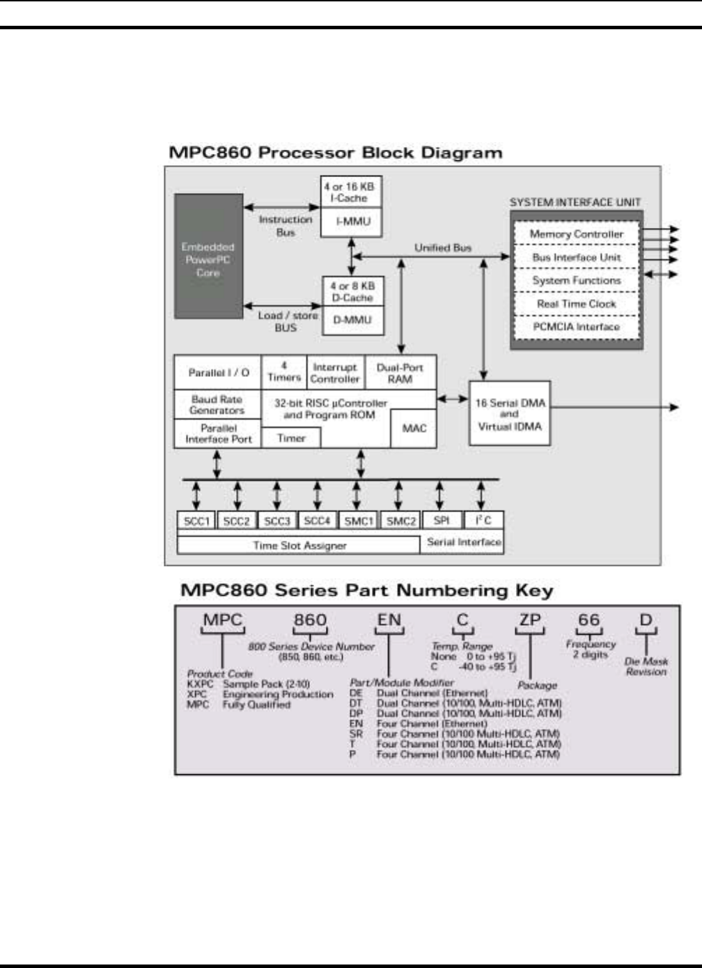
IC DATA
U9
Microprocessor, 66MHz
###### (Motorola, XPC860PZP66D4, BGA357)
MM101271V1 R1A 90
IC DATA
U10, U11
1M x 16/2M x 8 Flash, Simultaneous Read/Write
###### (AMD, AM29DL163DB90E1)
MM101271V1 R1A 91
IC DATA
U13
RS232 Transceiver, 5V, 2-TX, 2-RX
###### (MAXIM, MAX202CSE)
U14
EEPROM, I2C, 16k x 8, 3.3V
###### (Atmel, AT24C128N, SOIC8)
92 MM101271V1 R1A
IC DATA
U15, U26
I2C Bus 8-Bit I/O
###### (Philips, PCF8574A)
PIN IDENTIFICATION
SYMBO
LPIN DESCRIPTION
A0 1 Address Input 0
A1 2 Address Input 1
A2 3 Address Input 2
P0 4 Quasi-bidrectional I/O 0
P1 5 Quasi-bidrectional I/O 1
P2 6 Quasi-bidrectional I/O 2
P3 7 Quasi-bidrectional I/O 3
Vss 8 Supply Ground
P4 9 Quasi-bidrectional I/O 4
P5 10 Quasi-bidrectional I/O 5
P6 11 Quasi-bidrectional I/O 6
P7 12 Quasi-bidrectional I/O 7
INT 13 Interrupt Output (Active LOW)
SCL 14 Serial Clock Line
SDA 15 Serial Data Line
VDD 16 Supply Voltage
U16
Phase-Lock-Loop (PLL)
###### (TI, 74HCT4046ADB)
MM101271V1 R1A 93
IC DATA
U17, U20
Single Inverter
###### (Philips, 74HC1G04GW)
U18, U22, U23
HEX Buffer
###### (Philips, 74HC14PW)
94 MM101271V1 R1A
IC DATA
U19
Octal XCVR, BUS HOLD, 3.3V
###### (Philips, 74LVCH245APW)
U21
RS485 Transceiver
###### (TI, 75176BD)
MM101271V1 R1A 95
IC DATA
U24
RS232 Transceiver, 3V to 5.5V, 3-TX, 5-RX
###### (MAXIM, MAX3241CAI, SSOP28)
U25
+5V Regulator, 1.5A
###### (LINEAR TECH, LT1086CM-3.3)
96 MM101271V1 R1A
IC DATA
U27
144 PIN CPLD
###### (ALTERA, EPM3256ATC144)
MM101271V1 R1A 97
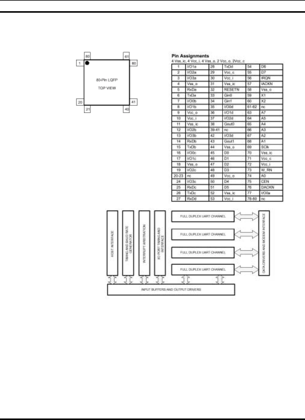
IC DATA
U28
QUAD UART (QUART)
###### (Philips, SC28L194A1BE)
98 MM101271V1 R1A
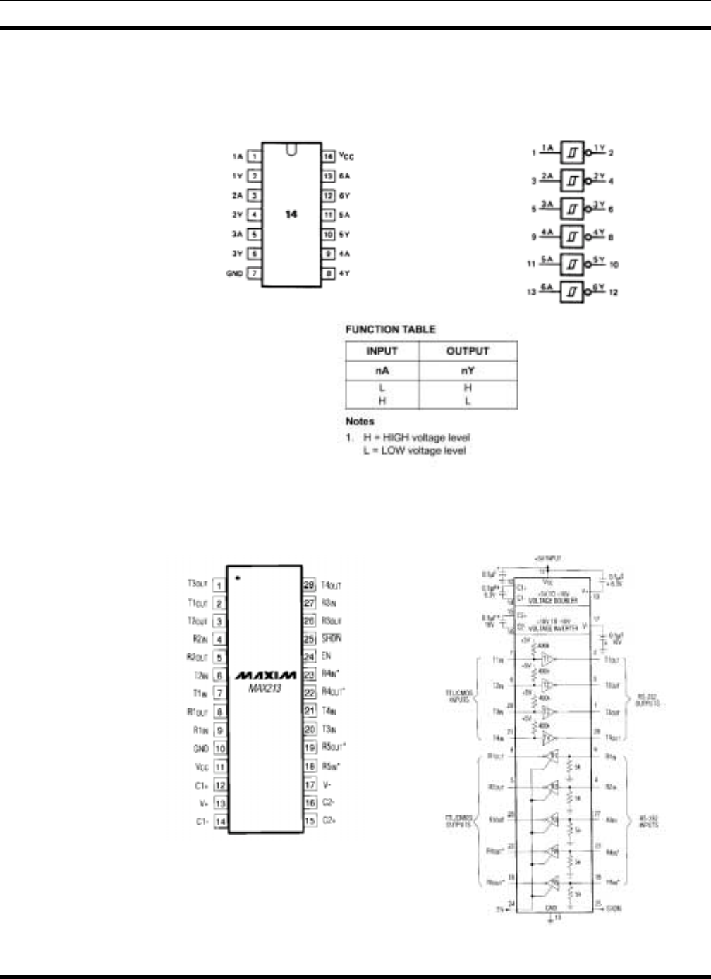
IC DATA
U29, U32
HEX Buffer
###### (Philips, 74HCT14PW)
U30
RS-232 Transceiver, 5V, 4-TX, 5-TX
###### (MAXIM, MAX213CAI)
MM101271V1 R1A 99
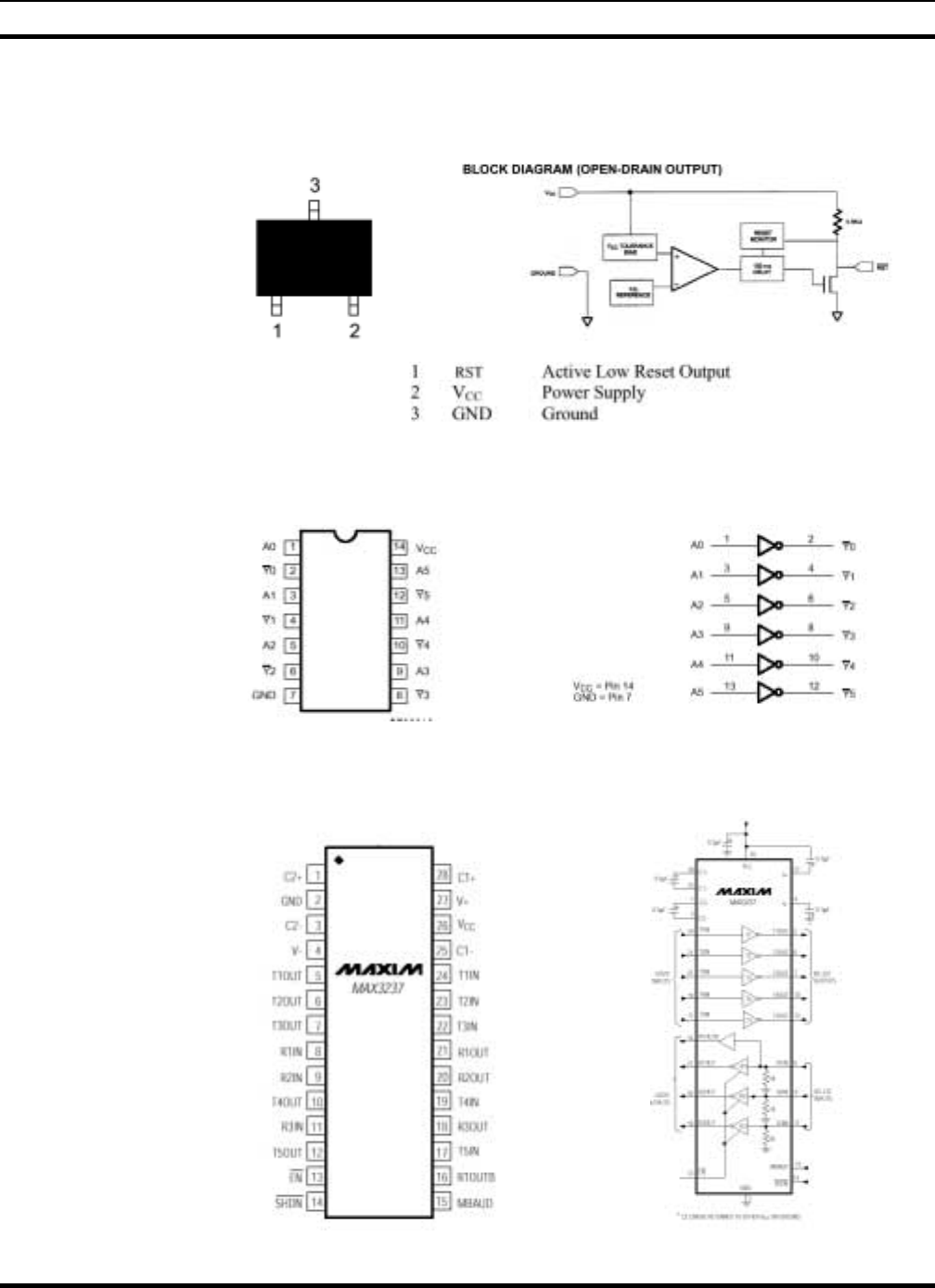
IC DATA
U31
Reset Supervisor
###### (Dallas, DS1818R-10)
U33, U34, U35, U39
HEX Open-Collector Output Drivers
###### (Philips, 74F06AD)
U36
RS232 Transceiver, 3V to 5.5V, 5-TX, 3-RX
###### (MAXIM, MAX3237CAI)
100 MM101271V1 R1A
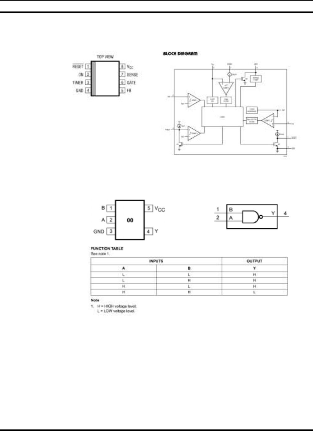
IC DATA
U37
Hot Swap Controller
###### (LINEAR TECH, LTC1422)
U38
Single NAND Gate
###### (Philips, 74AHC1G00GW)
MM101271V1 R1A 101
IC DATA
U40
555 Timer
###### (National, LMC555CM)
102 MM101271V1 R1A
IC DATA
6.8MODEM DAUGHTER BOARD (A8)
U1
Microprocessor
#### (Dallas 80C323)
MM101271V1 R1A 103
IC DATA
U2 & U4
64k x 8 SRAM
#### (IDT71V124SA)
U3
Dual Port RAM
#### (IDT70V05L55PF)
Continued
104 MM101271V1 R1A
IC DATA
Continued
U5
Address Decoder
#### (LVC138)
U6
3.3V – 5V Converter
#### (IDT74FCT)
U7
8-Bit Latch
#### (VC373A)
U8
########
#### (####)
U9
RF Modem
#### (TI ROP101688/4C)
U10
PL Modem
#### (####)
MM101271V1 R1A 105

IC DATA
U11
VDI Modem
#### (####)
U12
Adder Bus Buffer
#### (IDT74FCT163245C/A)
U13
Data Bus Buffer
#### (####)
U14
6.9ROCKWELL MODEM INTERFACE CARD (A3)
U1
Dual Mono Flip-Flops
RYT 306 2024/C (74HC4538D)
U2
MICROCIRCUIT
RYT 306 2019/C (74HC86)
U3
MICROCIRCUIT
RYT 108 6003/C (TLC555ID)
U4
Dual Operational Amplifiers
RYT 101 6164/1 (RC4558D)
106 MM101271V1 R1A
IC DATA
U5
RS232 3+3 Transceivers ±5V
RYT 109 6073/1 (Motorola, MC145406DW)
6.10ANALOG FILTER BOARD (A4)
U2
###### (Motorola, MC79M05BT)
U3
Dual 4-Stage Binary Ripple Counter
###### (Motorola, MC74HC393AD)
MM101271V1 R1A 107
IC DATA
U4
Remote 16-Bit I/O Expander for I2C-Bus
###### (Philips, PCF8575CTS)
U5 & U10
High Slew Rate, Wide Bandwidth, Single Supply Operational Amplifier
###### (Motorola, MC33074D)
U6, U15, U17, U19 & U28
High Slew Rate, Wide Bandwidth, Single Supply Operational Amplifier
###### (Motorola, MC33072D)
U7
Fault-Protected, High-Voltage Single 8-to-1/Dual 4-to-1 Multiplexers
###### (Maxim, MAX4508ESE)
108 MM101271V1 R1A
IC DATA
U8
Addressable Dual Digital Potentionmeter
###### (Dallas, DS1803Z-010)
U9, U18 & U22
SPST/SPDT Analog Switches
###### (Maxim, DG419DY)
U11
8th-Order, Lowpass, Switched-Capacitor Filters
###### (Maxim, MAX292ESA)
U12 & U33
Low Offset Voltage Dual Comparators
###### (Motorola, LM393D)
MM101271V1 R1A 109
IC DATA
U14 & U20
8th-Order, Lowpass, Elliptic, Switched-Capacitor Filters
###### (Maxim, MAX294EWE)
MM101271V1 R1A 110
IC DATA
PIN NAME FUNCTION
1 CLK Clock input – use internal or
external clock.
2 V- Negative Supply pin.
Dual supplies:
-2.375V to –5.5V.
Single supply: V-= 0V.
3OP
OUT Uncommitted Op-Amp Output
4 OP IN Inverting input to the
uncommitted op amp. The
noninverting op amp is internally
tied to GND.
5 OUT Filter Output
6 GND Ground. In single-supply
operation, GND must be biased
to the mid-supply voltage level.
7 V+ Positive Supply pin. Dual
supplies: +2.375V to +5.5V.
Single supply: +4.75V to +11.0V
8 IN Filter Input.
U16 & U25
###### (Linear Tech, LTC4861S)
U21
High Performance Switched Capacitor Universal Filter
###### (Linear Tech, LTC1059S)
MM101271V1 R1A 111
IC DATA
U23
8-Bit A/D and D/A Converter
###### (Philips, PCF8591TD)
U24
+5V-Powered, Multi-Channel RS-232 Drivers/Receivers
###### (Maxim, MAX232AESE)
U26
###### (Linear Tech, LTC4891S)
112 MM101271V1 R1A
IC DATA
U27
Dual Peripheral Drivers
###### (TI, SN75451BD)
U31
Fault-Protected, High-Voltage, Single 4-to-1/Dual 2-to-1 Multiplexers
###### (Maxim, MAX4534ESD)
U32
HEX Inverter
###### (Motorola, MC14069UBDR2)
•
MM101271V1 R1A 113

IC DATA
MM101271V1 R1A 114