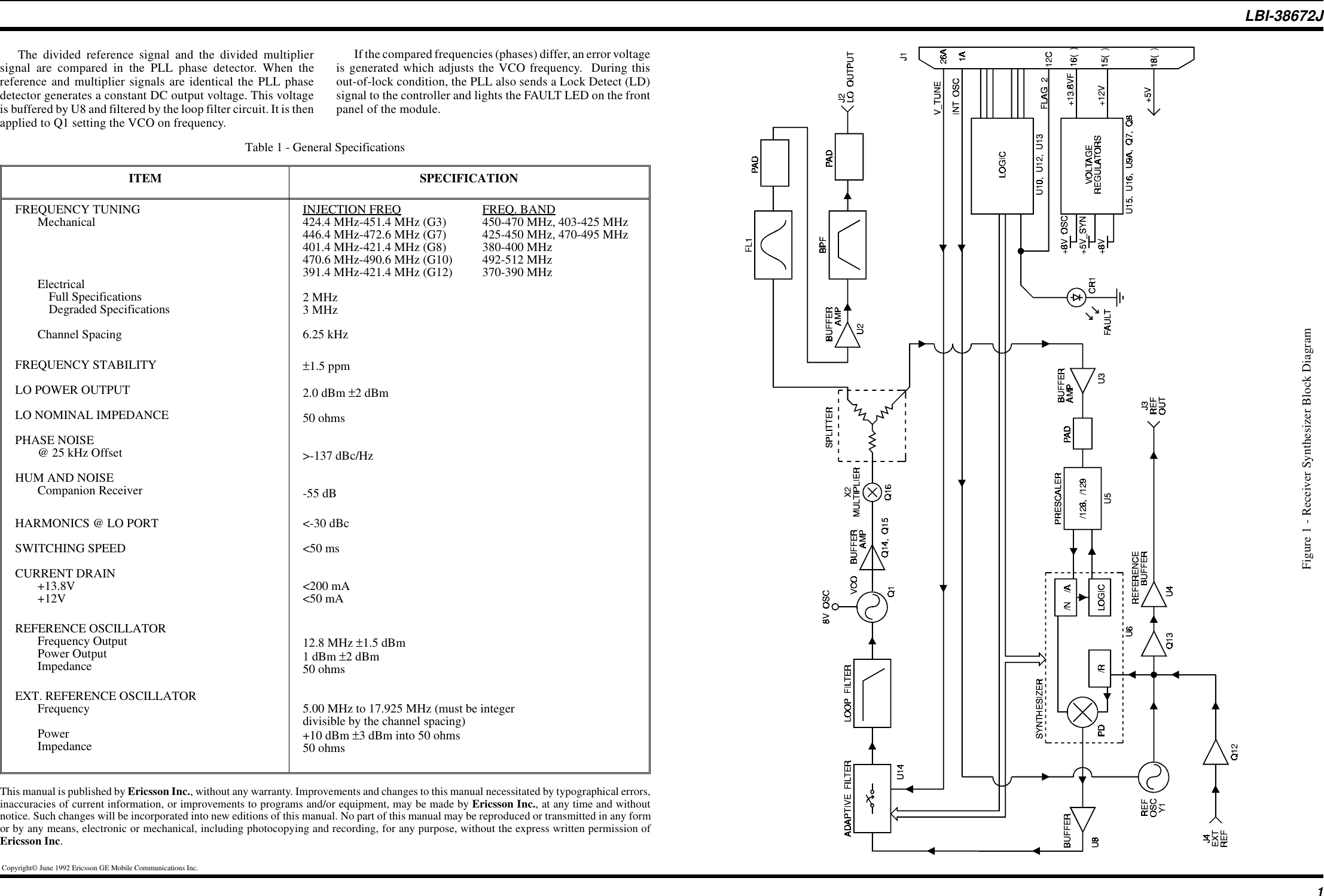
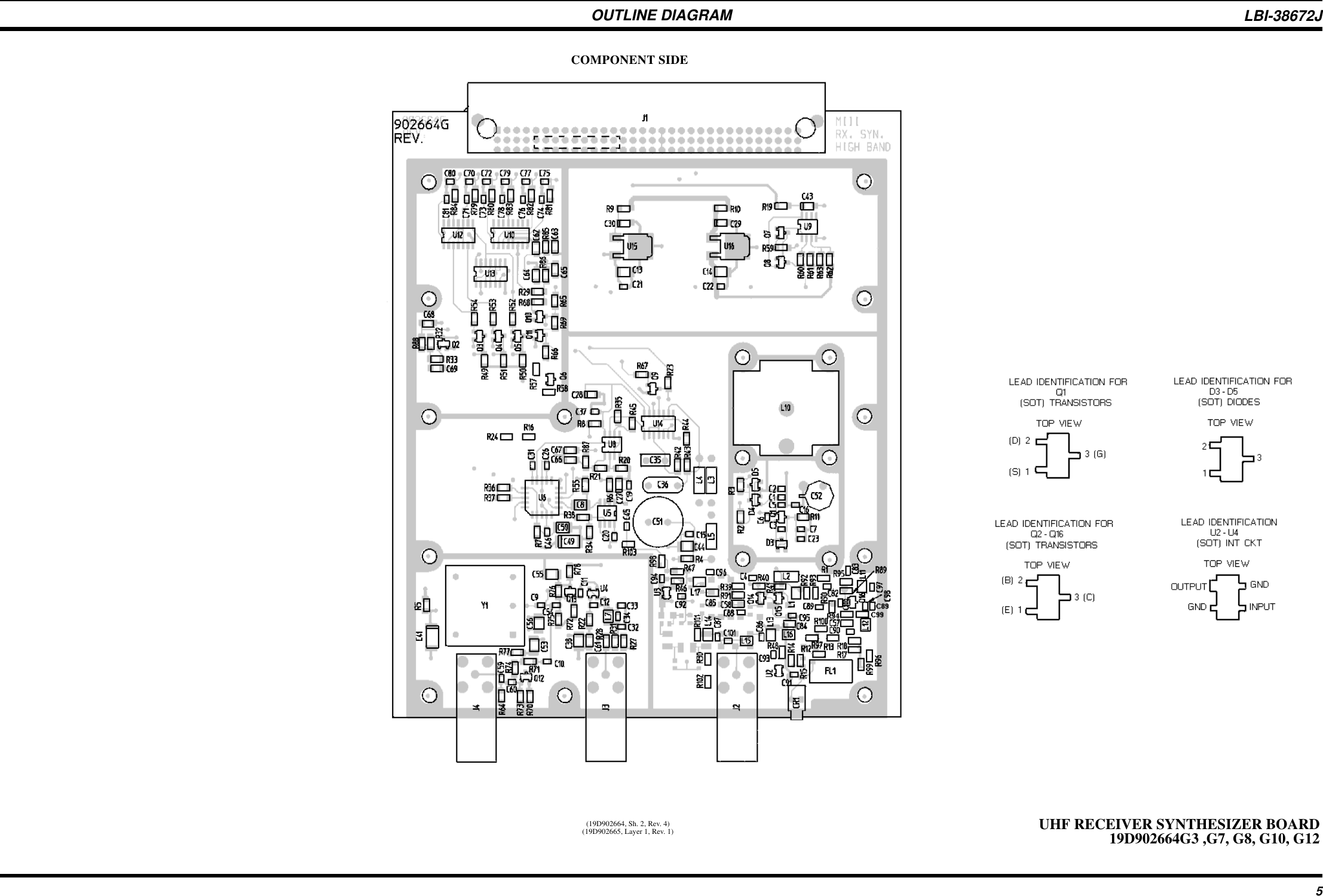
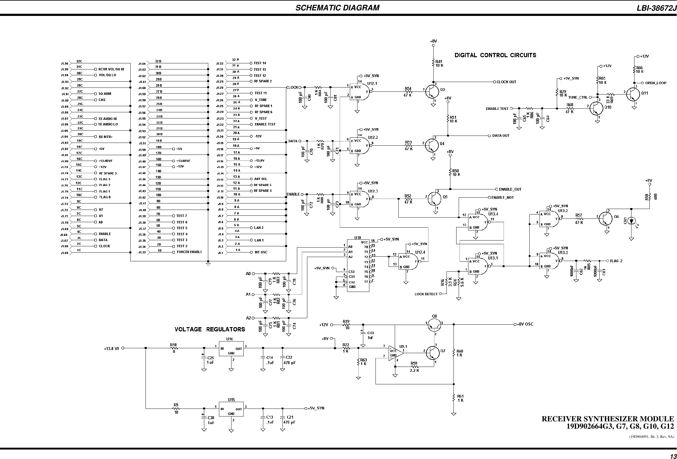
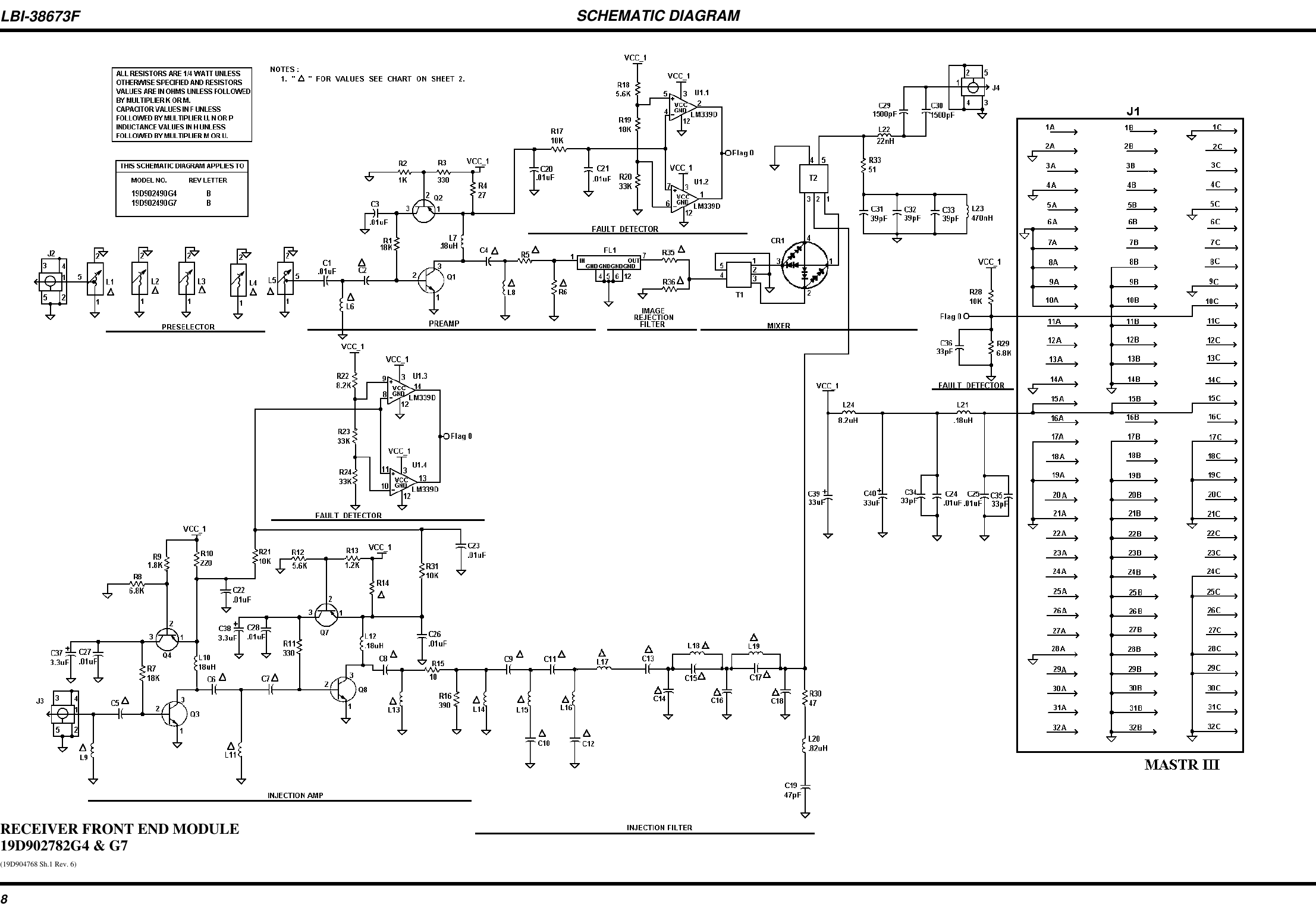
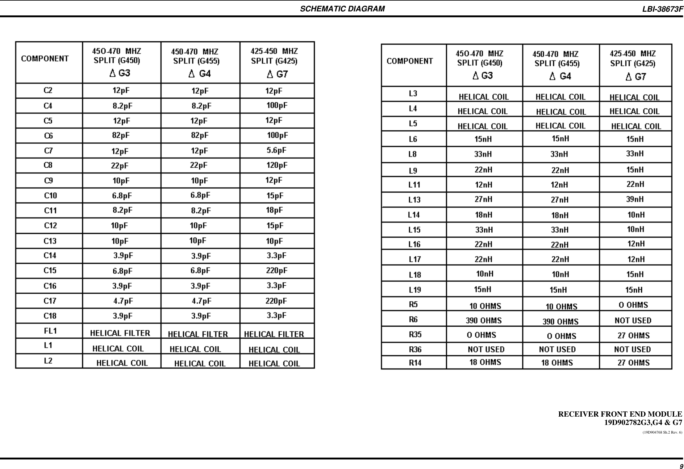
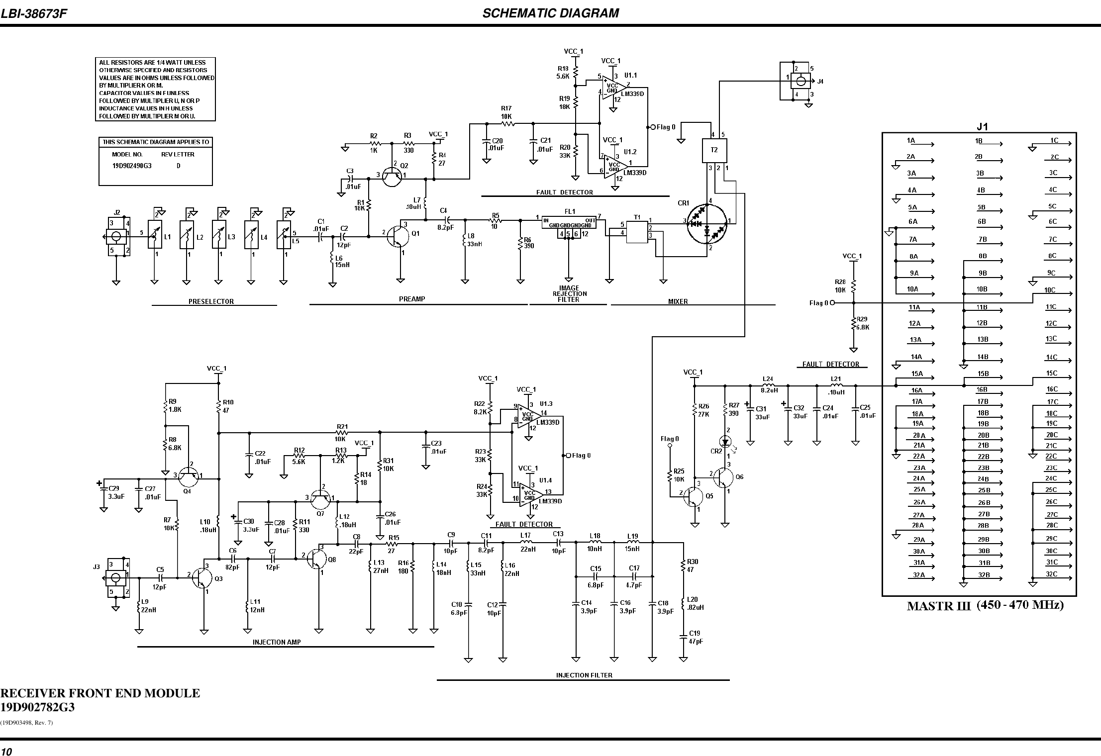
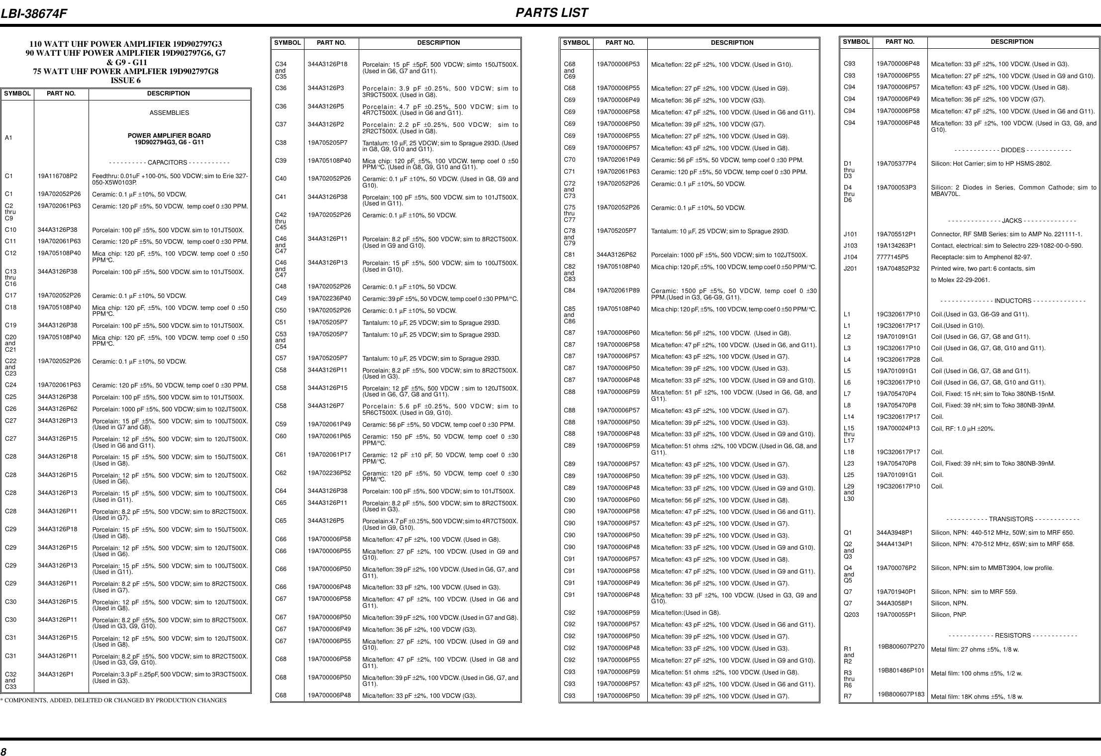
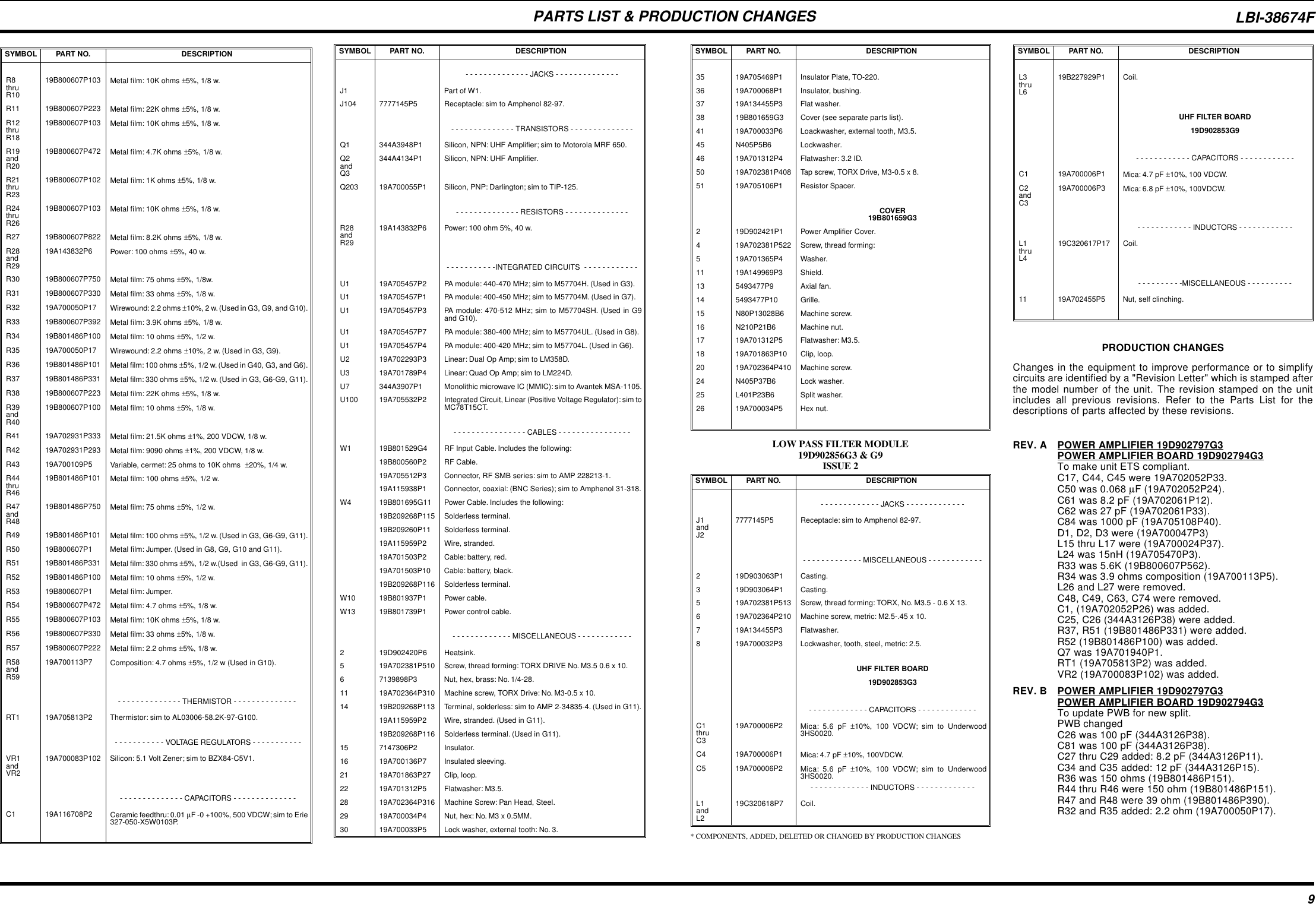
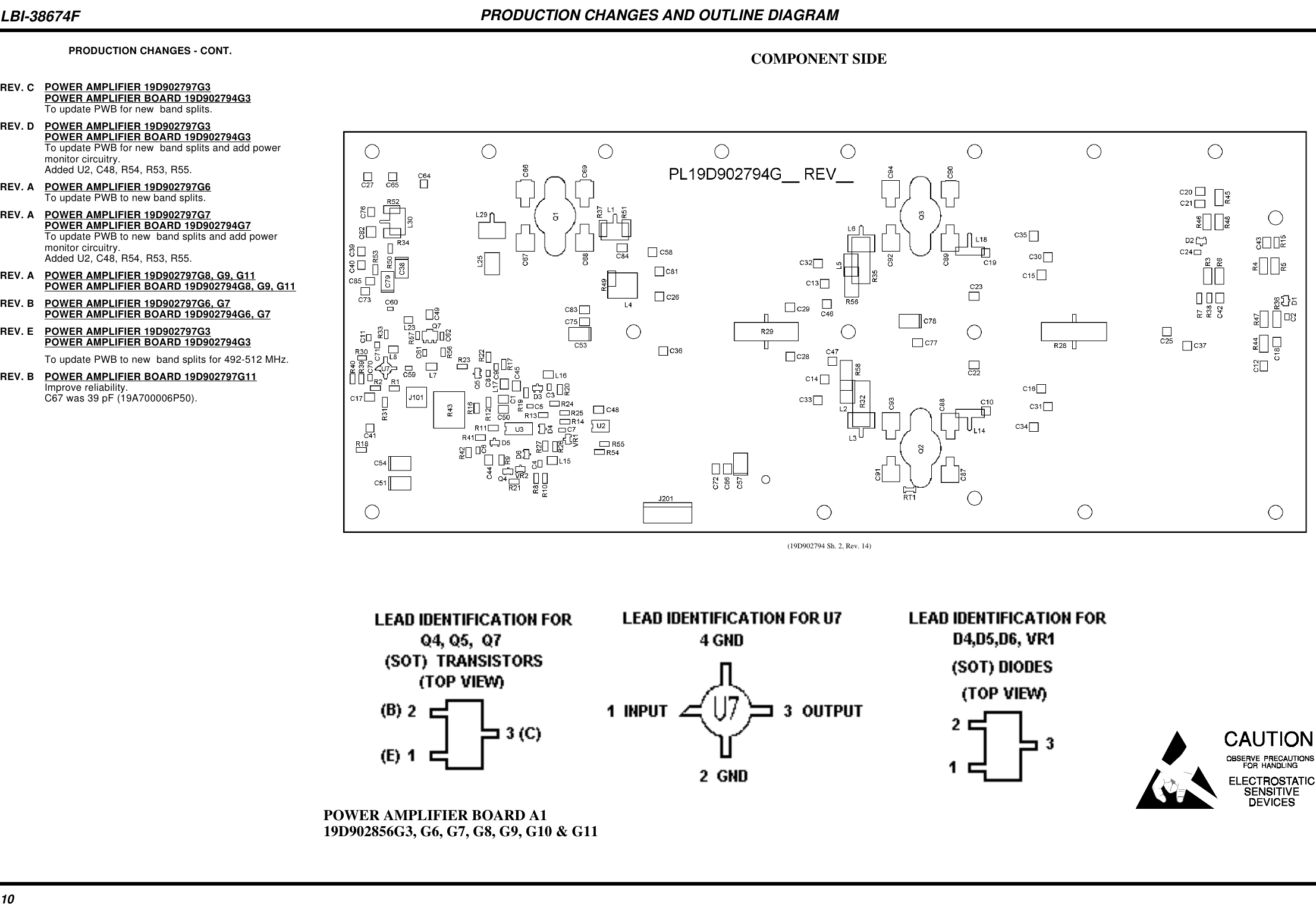
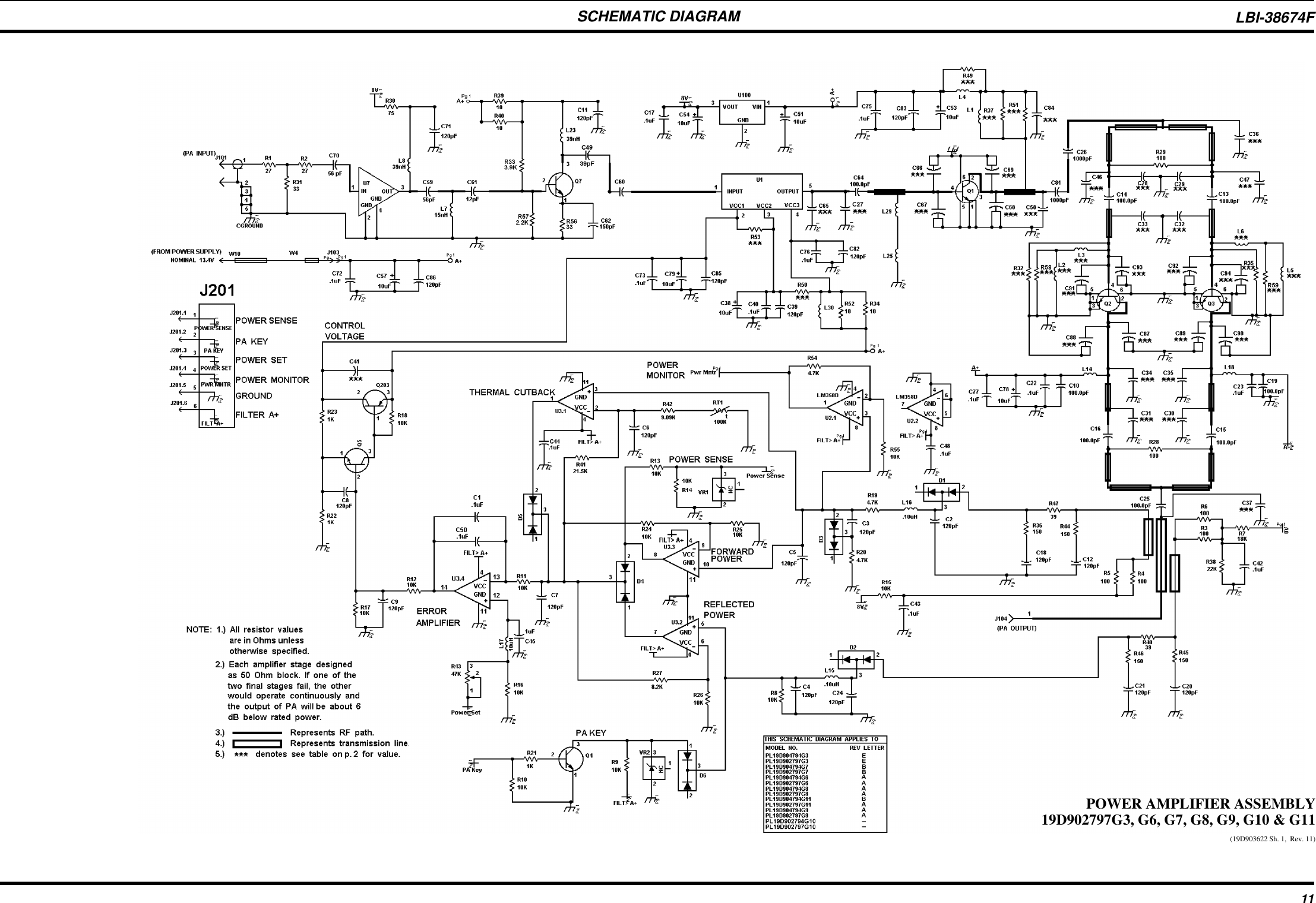
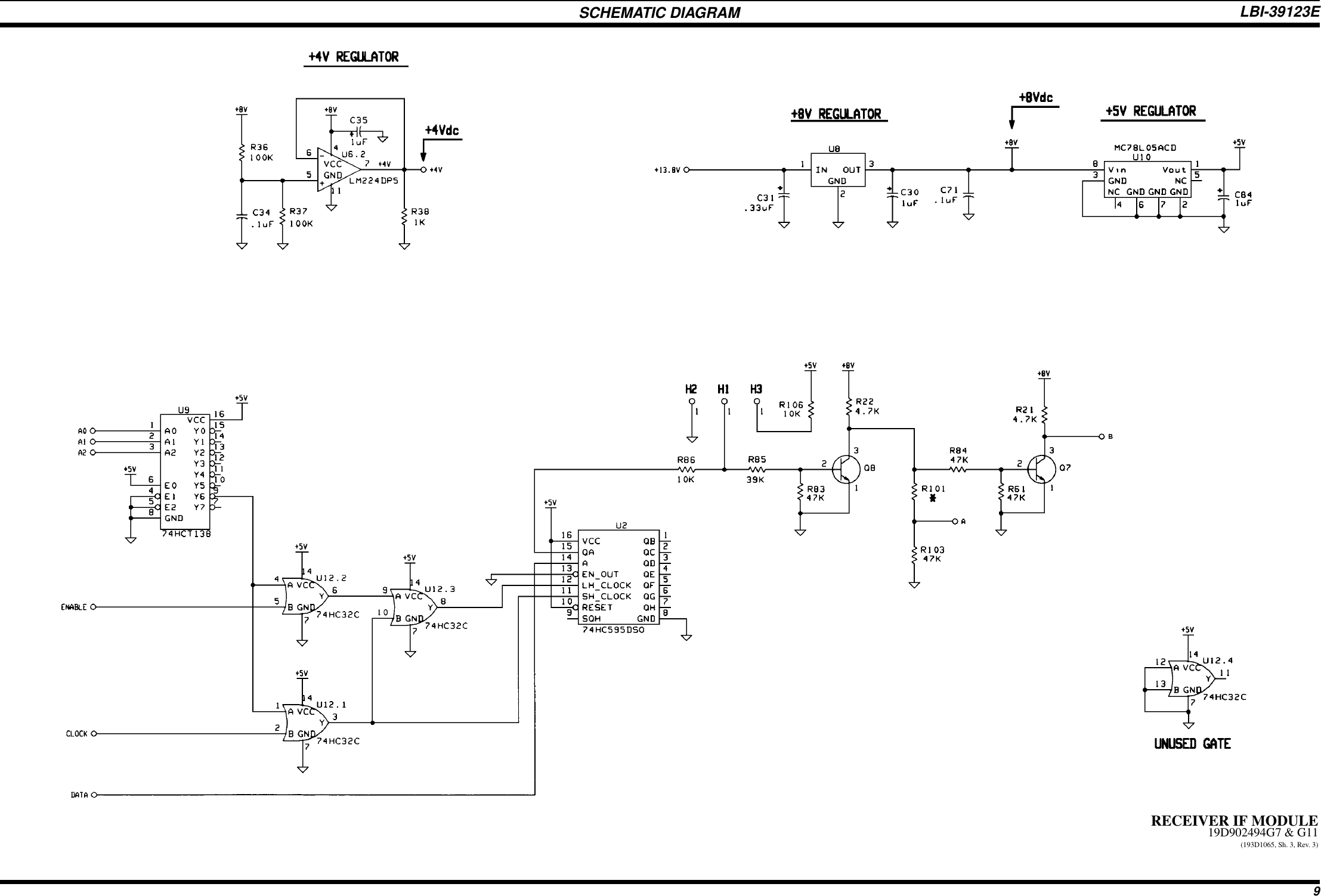
HARRIS TR-307-X2 PRIVIATE RADIO BASESTATION User Manual LBI 38643C 25 KHZ RECEIVER IF MODULE 19D902783G1
HARRIS CORPORATION PRIVIATE RADIO BASESTATION LBI 38643C 25 KHZ RECEIVER IF MODULE 19D902783G1
UserManual.wiki
>
HARRIS
>
TR-307-X2 User Manual
>
user manual
Contents
1.
user manual
2.
Manual
user manual
Navigation menu
Upload a User Manual
Namespaces
Wiki Guide
HTML
PDF
Info
Views
User Manual
Discussion / Help
Navigation
![If the biasing for the amplifiers is not within the properoperating range, the fault detector circuit will pull the FLAG0 line low. This turns off Q5 causing Q6 to conduct. Q6 nowprovides a ground path for CR2, turning on the fault indica-tor.MAINTENANCETEST PROCEDUREThe RXFE module has to be tested for Noise Figure,Gain, Third Order Intercept Point, Isolation etc.. With propercurrent drawing of devices, Bandwidth and Conversion Gainthe RXFE module will meet its specifications. The followingare test procedures will verify proper Conversion Gain andcurrent drain:1. Supply 12 Vdc to pin 15A, B, C. (1C is ground.)2. Inject the desired RF signal into RF IN at a level of-10 dBm.3. Inject the desired local oscillator signal into LO INat a level of 0 dBm [LO frequency = RF frequency -21.4 MHz (G3, G4) + 21.4 MHz (G7)].4. Measure the IF OUT power at 21.4 MHz, the ratio ofRF IN to IF OUT is -2 dB ±1 dB.5. Measure the current drawn by the RXFE module.Typical current drain is 290 mA.ALIGNMENT PROCEDUREAlignment for the Receiver Front End module consistsof tuning the five-pole Preselector Filter only. Normally, theRXFE should only need the fine-tuning procedures. For amajor receiver frequency change, the RXFE needs to beadjusted using the major-retuning procedures.For Fine-Tuning1. Supply 12 Vdc to pin 15A, B, C. (1C is ground.)2. Inject the desired RF signal into RF IN (J2) at a levelof -10 dBm.3. Inject the desired local oscillator signal into LO IN(J3) at a level of 0 dBm [LO frequency = RF fre-quency - 21.4 MHz (G3, G4) + 21.4 MHz (G7)].4. Detect IF signal at 21.4 MHz. Slightly adjust L1 toL5 to get maximum power (don’t adjust more thanten degrees). If an RF Voltmeter is used, connect aLow Pass Filter (LPF)to the IF OUT (J4) to attenuatehigh frequency components. The corner of the LPFshould be set for 40 MHz.5. Repeat Test Procedure steps to verify conversiongain and current drain.For Major RetuningThe best way to do a major retuning of the RXFE is withswept frequency tuning. The swept frequency tuning can bedone using a Spectrum Analyzer and Tracking Generator.With proper Injection power and current drain, the frequencyresponse of the Preselector Filter can be seen by viewing theRF to IF port feedthrough on the spectrum analyzer. Thisfeedthrough is typically 35 dB down from the input level atthe RF port. Use the following procedure for swept fre-quency tuning:1. Supply 12 Vdc to pin 15A, B, C. (1C is ground.)2. Inject the Tracking generator output at 0 dBm intothe RF IN connector, (J2).3. Inject local oscillator power at 0 dBm into the LO INconnector, (J3) [LO frequency = RF frequency - 21.4MHz (G3, G4) + 21.4 MHz (G7)].4. Preset the height of slugs with respect to the top offive-pole cavity as follows (Table 2):Table 25. Center the spectrum analyzer at the desired frequencyand set the reference at about -30 dBm. Adjust L1 toL5 for best possible response.HEIGHT (in inches)Frequency(MHz)L1 L2L3L4L5450 15/64 16/64 17/64 17/64 16/64454 16/64 17/64 17/64 18/64 15/64458 16/64 19/64 19/64 19/64 17/64462 18/64 19/64 20/64 20/64 18/64466 21/64 22/64 23/64 21/64 20/64470 22/64 24/64 24/64 23/64 22/64SYMPTOM AREAS TO CHECK READING (TYP.)LOW CONVERSION GAIN Check Vcc 12 VPreselector Loss 3.5 dBPreamplifier Gain 11 dBImage Rej. Filter Loss 2 dB1st Mixer Conversion Loss 6.5 dB1 L.O. Level (@ mixer L.O. +22 ±2 dBm (G3, G4)port) +14 ±2 dBm (G7)LED INDICATOR ON Check Vc of Q1 10 VCheck Vc of Q3 and Q8 10 VIF FREQUENCY OFF Check L.O. FREQUENCY L.O. frequency = RF frequency - 21.4 MHz (G3,G4) + 21.4 MHz (G7)LOW L.O. POWER* Injection Amplifier Gain 23 ±2 dB (G3, G4)18 ±2 dB (G7)Injection Filter Loss 2 dB*NOTE: For troubleshooting the gain or loss, the RXFE needs to be under the normal operating condition:•12 Vdc supply.•Inject L.O. power at a level of 0 dBm into LO IN (J3), [LO freq. = RF freq. - 21.4 MHz (G3, G4)+ 21.4 MHz (G7).•Inject the desired RF signal at a level of -10 dBm into RF IN (J2).•Terminate the IF OUT (J4) with a good 50 ohm impedance.•Use a Spectrum Analyzer and 50 ohm probe (with good RF grounding) to probe at the input and output ofeach stage to check its gain or loss (see schematic diagram).TROUBLESHOOTING GUIDELBI-38673F2](https://usermanual.wiki/HARRIS/TR-307-X2.user-manual/User-Guide-5051-Page-39.png)
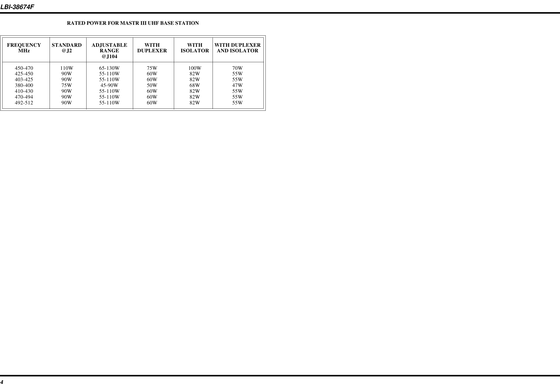
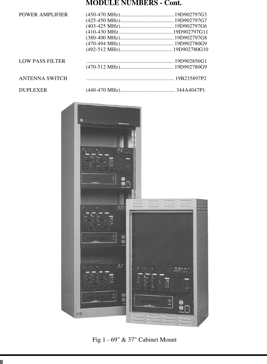
![GENERALCABINET INDOOR CABINET (Floor Mount)37" (CNV) 69"SIZE [in. (mm)]Height:Width:Depth:Weight (min) [(lb. (Kg)] Continuous Duty Packed , Domestic ShippingNumber of Rack UnitsMaximum Units w/Power SupplyMaximum Units w/o Power Supply37.0 (940)21.5 (550)18.25 (460)150 (68)165 (75)172269.1 (1750)23.1 (590)21 .0 (533)300 (136)317 (147)3334SERVICE SPEAKER: 1 Watt @ 8ΩSERVICE MICROPHONE: Transistorized DynamicDC 5A @ 120 VAC or 3A @ 230 VACDUTY CYCLE (EIA) Continuous: Transmit/Receive - 100%AMBIENT TEMPERATURE: -30oC to +60oC(or full spec performance per EIA) (-22oF to +140oF)HUMIDITY (EIA): 90% @ 50oC (122oF)INPUT POWER SOURCE: 120 VAC (± 20%) orOptional: 230 VAC (± 15%), 50 HzStandby Battery Source: 13.8 VDC, 100 AH (min.)ANTENNA CONNECTIONS: Type NLENGTH OF AC POWER CABLE: 10 ft (3048mm)METERING: Provided through Handset or TQ0619 Utility Software.ALTITUDEOperable: Up to 15,000 ft (4,570 m)Shipable: Up to 50,000 ft (15,250 m)SOURCE POWER DRAIN UHFFrequency Range(MHz) 380-400 403-430 425-450 450-470 470-494 492-512AC Input Power: 5A @ 120 VAC or 3A @ 230 VACDC Input Power: VDCTx (full / half power): 13.8Rx only: 13.8Tx (full / half power): 26.4EDACS Applications: 13.833/25A2 A2 A33/25A2 A2 A33/25A2 A2 A33/25A2 A2 A33/25A2 A2 A33/25A2 A2 ANOTE: One Rack Unit equals 1.75 inches, Stations occupy 8 rack units of cabinet space. LBI-38675E5](https://usermanual.wiki/HARRIS/TR-307-X2.user-manual/User-Guide-5051-Page-67.png)
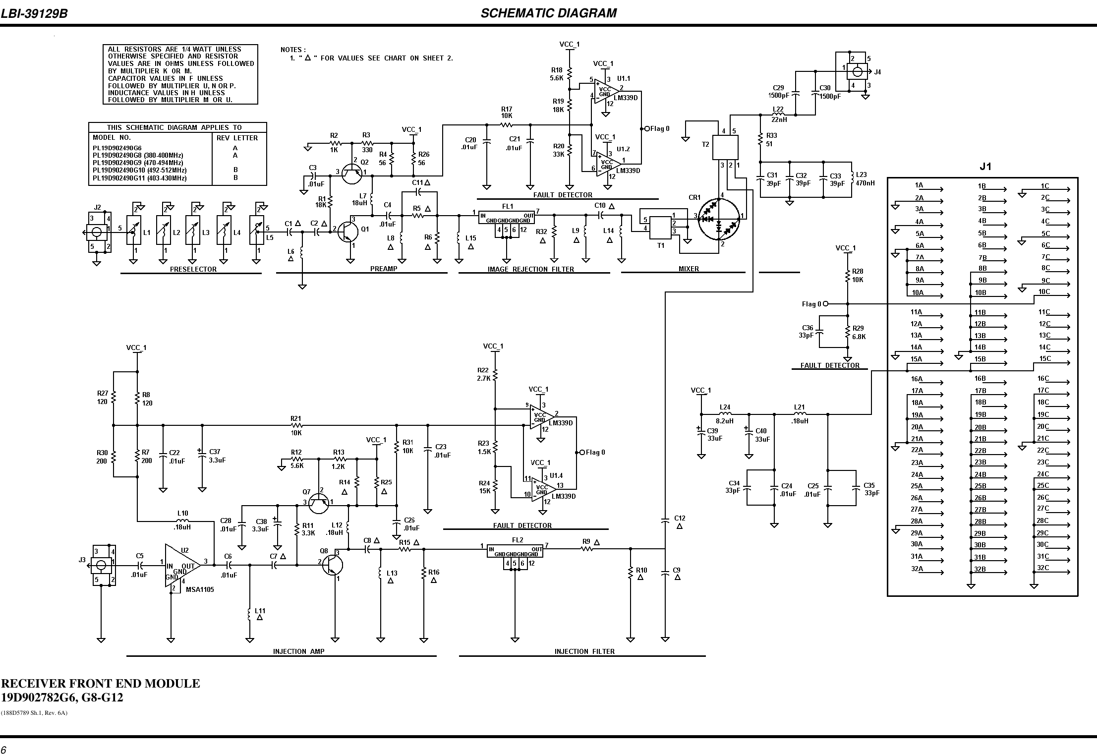
![MAINTENANCETEST PROCEDUREFollowing is a test procedure of the module to verifyproper Conversion Gain :1. Supply 12 Vdc to pin 15A, B, C. (1C is ground.)2. Inject the desired RF Frequency into RF IN at a levelof -10 dBm.3. Inject the desired local oscillator frequency into LOIN at a level of 0 dBm [LO frequency = RF frequency- 21.4 MHz (for groups G9, G10), or, LO frequency= RF frequency + 21.4 MHz (for groups G6, G8,G11, G12)].4. Measure the IF OUT power at 21.4 MHz, the ratio ofRF IN to IF OUT should be -1.5 ±1.5 dB.5. Measure the current drawn by the RXFE module.Typical current drain is 180 to 230 mA.ALIGNMENT PROCEDUREAlignment for the Receiver Front End module consistsof tuning the five-pole Preselector Filter only. The ImageRejection Filter and LO injection filter are not to be tuned.Normally, the RXFE should only need the fine-tuning pro-cedure. For a major receiver frequency change, the RXFEshould be adjusted using the major-retuning procedure.For Fine-Tuning1. Supply 12 Vdc to pin 15A, B, C. (1C is ground.)2. Inject the desired RF Frequency into RF IN (J2) at alevel of -10 dBm.3. Inject the desired local oscillator frequency into LOIN (J3) at a level of 0 dBm [LO frequency = RFfrequency - 21.4 MHz (for groups G9, G10), or, LOfrequency = RF frequency + 21.4 MHz (for groupsG6, G8, G11, G12)].4. Detect IF signal at 21.4 MHz. Slightly adjust L1 toL5 to get maximum power (don’t adjust more than1/4 turn). If an RF Voltmeter is used, connect a LowPass Filter (LPF)to the IF OUT (J4) to attenuate highfrequency components. The corner of the LPF shouldbe set for 40 MHz.5. Repeat Test Procedure steps to verify conversiongain.For Major RetuningThe best way to do a major retuning of the RXFE is withswept frequency tuning. The swept frequency tuning can bedone using a Spectrum Analyzer and Tracking Generator.With proper Injection level the frequency response of thePreselector Filter can be seen by viewing the RF to IF portfeedthrough on the spectrum analyzer. This feedthrough istypically 35 dB down from the input level at the RF port. Usethe following procedure for swept frequency tuning:1. Supply 12 Vdc to pin 15A, B, C. (1C is ground.)2. Inject the Tracking generator output at 0 dBm intothe RF IN connector, (J2).3. Inject local oscillator power at 0 dBm into the LO INconnector, (J3) [LO frequency = RF frequency - 21.4MHz (for groups G9, G10), or, LO frequency = RFfrequency + 21.4 MHz (for groups G6, G8, G11,G12)].4. Preset the height of slugs with respect to the top offive-pole cavity as follows (Table 2):5. Center the spectrum analyzer at the desired frequencyand set the reference at about -30 dBm. Adjust L1 toL5 for best possible response.SYMPTOM AREAS TO CHECK READING (TYP.)LOW CONVERSION GAIN Check Vcc 12 VPreselector Loss 3 dBPreamplifier Gain 11 dBImage Rej. Filter Loss 2 dB1st Mixer Conversion Loss 7 dBFAULT INDICATOR LOW Check Vc of Q1 9 TO 10VCheck Vc of U2 5 TO 6 VCheck Vc of Q8 9 TO 10 VIF FREQUENCY OFF Check L.O. FREQUENCY L.O. frequency=RF frequency - 21.4 MHz (G9,G10) + 21.4 MHz (G6, G8, G11, G12)LOW L.O. POWER* Injection Amplifier Gain approx 20 dB GainInjection Filter Loss 2 dB*NOTE: For troubleshooting the gain or loss, the RXFE needs to be under the normal operating condition:•12 Vdc supply.•Inject L.O. power at a level of 0 dBm into LO IN (J3), [LO freq. = RF freq. - 21.4 MHz (G9, G10) or, LO frequency = RF frequency + 21.4 MHz (G6, G8, G11, G12)].•Inject the desired RF signal at a level of -10 dBm into RF IN (J2).•Terminate the IF OUT (J4) with a good 50 ohm impedance.•Use a Spectrum Analyzer and 50 ohm probe (with good RF grounding) to probe at the input and output ofeach stage to check its gain or loss (see schematic diagram).TROUBLESHOOTING GUIDEG6 & G11 HEIGHT (in inches)Frequency (MHz) L1 L2 L3 L4 L5403 12/64 10/64 12/64 13/64 12/64408 13/64 13/64 14/64 14/64 13/64413 14/64 14/64 14/64 15/64 14/64418 16/64 16/64 15/64 16/64 15/64423 17/64 17/64 16/64 18/64 16/64Table 2G9 HEIGHT (in inches)Frequency(MHz) L1 L2 L3 L4 L5470 12/64 12/64 12/64 12/64 12/64474 13/64 13/64 13/64 13/64 13/64478 14/64 14/64 14/64 14/64 14/64482 15/64 15/64 15/64 15/64 15/64486 16/64 16/64 16/64 16/64 16/64490 17/64 17/64 17/64 17/64 17/64492 18/64 18/64 18/64 18/64 18/64G10 HEIGHT (in inches)Frequency(MHz) L1 L2 L3 L4 L5492 12/64 10/64 10/64 10/64 8/64497 12/64 10/64 12/64 12/64 9/64502 14/64 12/64 13/64 14/64 10/64507 15/64 15/64 16/64 16/64 12/64512 17/64 16/64 17/64 17/64 14/64G8, G12 HEIGHT (in inches)Frequency(MHz) L1 L2 L3 L4 L5380 16/64 16/64 16/64 16/64 16/64385 17/64 17/64 17/64 17/64 17/64390 18/64 18/64 18/64 18/64 18/64395 19/64 19/64 19/64 19/64 19/64400 20/64 20/64 20/64 20/64 20/64370 14/64 14/64 14/64 14/64 14/64375 15/64 15/64 15/64 15/64 15/64LBI-39129B2](https://usermanual.wiki/HARRIS/TR-307-X2.user-manual/User-Guide-5051-Page-87.png)