HARRIS TR-307-X2 PRIVIATE RADIO BASESTATION User Manual LBI 38643C 25 KHZ RECEIVER IF MODULE 19D902783G1
HARRIS CORPORATION PRIVIATE RADIO BASESTATION LBI 38643C 25 KHZ RECEIVER IF MODULE 19D902783G1
HARRIS >
Contents
- 1. user manual
- 2. Manual
user manual

TABLE OF CONTENTS
Page
DESCRIPTION . . . . . . . . . . . . . . . . . . . . . . . . . . . . . . . . . . . . . . . . . . . . Front Cover
GENERAL SPECIFICATIONS . . . . . . . . . . . . . . . . . . . . . . . . . . . . . . . . . . . . 1
CIRCUIT ANALYSIS . . . . . . . . . . . . . . . . . . . . . . . . . . . . . . . . . . . . . . . . . 1
INPUT MATCHING NETWORK . . . . . . . . . . . . . . . . . . . . . . . . . . . . . . . 1
CRYSTAL FILTERS, IF AMPLIFIERS . . . . . . . . . . . . . . . . . . . . . . . . . . . . 1
OSCILLATOR/MIXER/DETECTOR . . . . . . . . . . . . . . . . . . . . . . . . . . . . . 1
AUDIO AMPLIFIER . . . . . . . . . . . . . . . . . . . . . . . . . . . . . . . . . . . . . . 1
SQUELCH . . . . . . . . . . . . . . . . . . . . . . . . . . . . . . . . . . . . . . . . . . . . 1
Buffer Amplifier . . . . . . . . . . . . . . . . . . . . . . . . . . . . . . . . . . . . . . 1
High Pass Filter . . . . . . . . . . . . . . . . . . . . . . . . . . . . . . . . . . . . . . . 2
Noise Detector . . . . . . . . . . . . . . . . . . . . . . . . . . . . . . . . . . . . . . . 2
DC Amplifier . . . . . . . . . . . . . . . . . . . . . . . . . . . . . . . . . . . . . . . . 2
Schmitt Trigger . . . . . . . . . . . . . . . . . . . . . . . . . . . . . . . . . . . . . . . 2
FAULT DETECTOR . . . . . . . . . . . . . . . . . . . . . . . . . . . . . . . . . . . . . . 2
VOLTAGE REGULATOR . . . . . . . . . . . . . . . . . . . . . . . . . . . . . . . . . . . 2
MAINTENANCE . . . . . . . . . . . . . . . . . . . . . . . . . . . . . . . . . . . . . . . . . . . 2
BLOCK DIAGRAM . . . . . . . . . . . . . . . . . . . . . . . . . . . . . . . . . . . . . . . . . 2
RECOMMENDED TEST EQUIPMENT . . . . . . . . . . . . . . . . . . . . . . . . . . . . 2
ALIGNMENT PROCEDURE . . . . . . . . . . . . . . . . . . . . . . . . . . . . . . . . . 2
TROUBLESHOOTING . . . . . . . . . . . . . . . . . . . . . . . . . . . . . . . . . . . . . 3
ASSEMBLY DIAGRAM . . . . . . . . . . . . . . . . . . . . . . . . . . . . . . . . . . . . . . . 3
OUTLINE DIAGRAM . . . . . . . . . . . . . . . . . . . . . . . . . . . . . . . . . . . . . . . . 4
SCHEMATIC DIAGRAM . . . . . . . . . . . . . . . . . . . . . . . . . . . . . . . . . . . . . . 5
PARTS LIST . . . . . . . . . . . . . . . . . . . . . . . . . . . . . . . . . . . . . . . . . . . . . . 7
PRODUCTION CHANGES . . . . . . . . . . . . . . . . . . . . . . . . . . . . . . . . . . . . . 8
IC DATA . . . . . . . . . . . . . . . . . . . . . . . . . . . . . . . . . . . . . . . . . . . . . . . . 9
MAINTENANCE MANUAL FOR
25kHz RECEIVER IF MODULE
19D902783G1
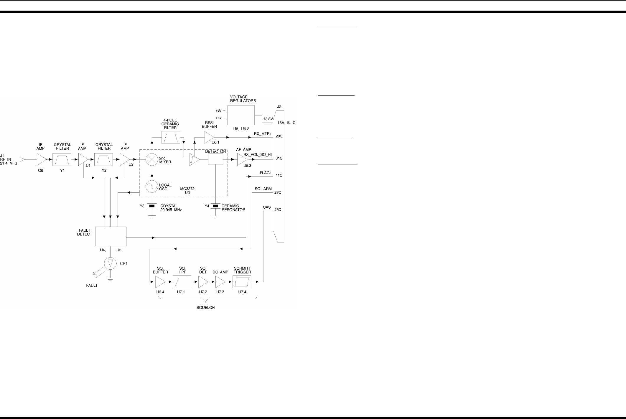
DESCRIPTION
The MASTR III Receiver IF Module provides ampli-
fication and demodulation of the 21.4 MHz Intermediate
Frequency signal. The IF Module also includes the re-
ceiver squelch circuitry. However, it does not include de-
emphasis or squelch audio gating circuits. Figure 1 is a
block diagram showing the functional operation of the
IF Module.
The IF Module circuitry contains the following:
•A 50 ohm input impedance matching network and
IF Amplifier
•A chain of two crystal filters and two integrated
circuit IF amplifiers
•An integrated circuit containing a crystal
oscillator, mixer, limiter, and quadrature detector
•A variable gain AF amplifier
•A squelch circuit
•A fault detector circuit
•An integrated circuit voltage regulator
LBI-38643C
ericssonz
Ericsson Inc.
Private Radio Systems
Mountain View Road
Lynchburg, Virginia 24502
1-800-528-7711 (Outside USA, 804-592-7711) Printed in U.S.A.
CIRCUIT ANALYSIS
INPUT MATCHING NETWORK
The input impedance matching network provides a 50 ohm
load for the receiver RF module. The network consists of C1
thru C3, L1 thru L3, and R1.
Capacitor C1 provides AC coupling and a DC block on the
input line (J1). This DC block protects the module in the event
of a failure in a preceding module. L2 and L3 are series reso-
nant at 21.4 MHz and provide a signal path to the FET ampli-
fier Q6. Parallel resonant circuit, L1 and C2, provide a path to
the 50 ohm load, R1, for frequencies other than 21.4 MHz.
CRYSTAL FILTERS, IF AMPLIFIERS
Y1, Y2, U1, U2, and associated circuitry provide IF filter-
ing and amplification at 21.4 MHz. Filters Y1 and Y2 are both
4 pole bandpass filters with a center frequency of 21.4 MHz
and a bandwidth of ±6.5 kHz. Amplifiers U1 and U2 are inte-
grated circuit amplifiers. U1 provides 30 dB of gain, U2 pro-
vides 18 dB of gain. The amplifiers and filters have terminal
impedances of 50 ohms. In circuit gain measurements can be
made using a high impedance probe.
Inductors L3, L4 and associated resistors and capacitors
provide power supply decoupling. R3 and R7 provide paths to
the input of the Fault Detector circuit. These inputs enable the
Fault Detector circuit to monitor the DC voltages of U1 and
U2.
The RF level detectors consist of transistors Q1 and Q2
along with associated resistors and capacitors. These detectors
play no role in the normal operation of the IF Module, but they
aid in unit testing and module troubleshooting.
OSCILLATOR/MIXER/DETECTOR
Integrated circuit U3 provides several functions including
2nd mixer, if amplifier and limiter, and quadrature detector.
The 20.945 MHz crystal oscillator provides local oscillator
injection to the mixer in U3. This mixer converts the 21.4 MHz
IF signal to 455 kHz. C20 and C21 are oscillator feedback ca-
pacitors and have been chosen to provide the proper capaci-
tance for crystal Y3. The proper oscillator output level is
difficult to measure directly without affecting the oscillation.
A preferable measurement is at TP3 which should read
about 50 mV pk. (Measured using a 10 megohm, 11 pF oscil-
loscope probe.)
The mixer is internally connected to the crystal oscillator.
Pins 16 and 3 of U3 are the mixer input and output respec-
tively. Typical mixer conversion gain is about 20 dB. The out-
put of the mixer drives the 4 pole ceramic bandpass filter FL1.
The limiter input is U3 pin 5, but the limiter output is inter-
nally connected to the detector and is not externally available.
A received signal strength indicator (RSSI) is provided at
U3 Pin 13. This indicator signal is generated within the limiter
circuitry and provides an output current proportional to the
logarithm of the input signal strength. This current develops a
voltage across R18. The voltage varies from about 0.7 Vdc for
noise input, to about 1 Vdc for a 12 dB SINAD signal, to a
maximum of about 2.7 Vdc for a high signal level (50 dB
stronger than that required for 12 dB SINAD).
The quadrature detector provides a demodulated audio fre-
quency output. The input to the detector is internally connected
to the limiter and is not externally available. The output of the
detector is U3 pin 9. R19 and C28 provide low-pass filtering to
remove 455 kHz feedthrough. Ceramic resonator Y4 provides
the frequency selective component needed for FM demodula-
tion. Y4 replaces the typical LC resonant circuit found in most
quadrature detectors. In contrast to the typical LC network, Y4
requires no adjustment.
The DC supply to U3 is provided through voltage dropping
resistor R11 to U3 pin 4. R12 provides a path to the input of
the Fault Detection circuit. This enables the Fault Detector to
monitor the DC voltage on U3.
AUDIO AMPLIFIER
Operational amplifier U6.3 provides audio frequency am-
plification. Its gain is set by its associated resistors, including
variable resistor VR1. VR1 allows for adjusting the AF output
level to 1 Vrms with a standard input signal to the module (1
kHz AF, 3 kHz peak deviation). U6.2 is used as a voltage regu-
lator to provide 4 Vdc for biasing the Operational amplifier.
SQUELCH
Buffer Amplifier
Integrated circuit U6.4 is configured as a unity gain buffer
amplifier. It provides a high input impedance to minimize load-
ing of the previous circuits.
Copyright© February 1992, Ericsson Inc.
TABLE 1 - GENERAL SPECIFICATIONS
ITEM SPECIFICATION
I.F. frequency 21.4 MHz
Input Impedance 50 ohm
12 dB SINAD -120.0 dBm
Adj. CH SEL (25 kHz) -103 dB
Image (20.49 MHz) -100 dB
3rd order Intercept Pt 23 dBm
Variation of Sensitivity with Signal Frequency 2 kHz
2nd I.F. frequency 455 kHz
2nd L.O. frequency 20.945 MHz
AF output (J2 pin 31C) 1 Vrms adjustable (with standard input signal)
AF output impedance 1k ohm
AF distortion 5%
AF response
10 Hz -3 dB
300 Hz ±1 dB
1000 Hz 0 dB reference
3 kHz ±1 dB
Hum & Noise -55 dB
RSSI output (J2 pin 20C) 0.7 to 2.7 Vdc prop to log (sig level)
RSSI time constant 5 ms
SQ Threshold Sensitivity -119 dBm
SQ Maximum Sensitivity -102 dBm
SQ Clipping 3 kHz
SQ Attack 150 ms
SQ Close 250 ms
SQ output (J2 pin 26C) 5V logic (low = squelched)
Fault output (J2 pin 11C) 5V logic (low = fault)
DC Supply 1 Vrms (adjustable)
LBI-38643C
1
Highpass Filter
The audio frequency highpass filter consists of U7.1 and its
associated circuitry. The purpose of this filter is to reject all
voice frequencies and allow only demodulated noise to pass.
The functioning of the squelch circuit depends upon the pres-
ence or absence of this noise. (When a signal is being received,
i.e. the receiver is quiet, the squelch circuit senses the absence
of noise and unsquelches the radio.)
Noise Detector
U7.2 along with associated components act as a noise de-
tector. The rectified output of U7.2 charges C44 to a nearly
constant DC voltage.
DC Amplifier
U7.3 is configured as a basic amplifier with a gain of 11.
Schmitt Trigger
U7.4 is configured as an amplifier with positive feedback.
This arrangement provides hysteresis in the output verses input
characteristic. This eliminates the possibility of the squelch cir-
cuit repeatedly cutting in and out when the input signal is near
a threshold. R56 and R57 act as a voltage divider to provide a 5
volt logic level output. (Logic High = unsqelched)
FAULT DETECTOR
U4 and U5 are voltage comparators. These are configured
into four "window detectors" which sense the presence of volt-
ages within specified ranges (windows).
The four window detector circuits are U4.1 & U4.2, U4.4
& U4.3, U5.1 & U5.2, and U5.4 & U5.3. These monitor DC
operating voltages on U6.2, U1, U2, and U3 respectively. R29
and R30 comprise a voltage divider to provide a 5 volt logic
level output. A fault is indicated when the output drops to zero.
Diode D1 and transistor Q3 monitor the output of the 8V
regulator. D1 is a 8.2 volt breakdown diode. If the regulator
output voltage should rise above 8.9 V (8.2 + 0.7 base-emitter
drop) Q1 will turn on and a fault will be indicated.
Transistors Q4 and Q5 are drivers for the front panel LED
CR1. These are powered from the +13.8 Vdc line before the
8V regulator. Therefore, if the regulator opens, a fault will still
be indicated.
VOLTAGE REGULATOR
U8 is a monolithic integrated circuit voltage regulator pro-
viding 8 Vdc. This powers all circuitry in the module with ex-
ception of the front panel LED and its drivers.
MAINTENANCE
RECOMMENDED TEST EQUIPMENT
The following test equipment is required to test the IF
Module.
1. FM Signal Generator; HP 8640B, HP 8657A, or
equivalent
2. AF Generator or Function Generator
3. Audio Analyzer; HP 8903B, HP 339A, or equivalent
4. Oscilloscope
5. DC Meter for troubleshooting
6. Power Supply; 13.8 Vdc @ 150 mA
ALIGNMENT PROCEDURE
1. Apply 13.8 Vdc supply to module.
2. Verify DC current consumption is between 90 and 150
mA.
3. Verify fault output is 0 to 0.5 Vdc and front panel LED
is off.
4. Apply a standard input signal to the module input. (-60
dBm, 21.4 MHz signal modulated with 1kHz AF, 3 kHz
peak deviation)
5. Set VR1 for 1 Vrms ±3% at module output (pin 31C on
96 pin connector J2).
Figure 1 - 25 kHz Receiver IF Module
LBI-38643C
2
TROUBLESHOOTING
Each IF amplifier has a nominal 18 dB gain. U2 has a
nominal gain of 30 dB. The mixer has about 20 dB gain with
proper LO injection. The proper crystal oscillator level is 50
mV pk measured at TP3.
The following four test points are provided on the PWB for
additional test capability:
TP1: 100 mV pk @ 21.4 MHz with -30 dBm input sig-
nal
TP2: 100 mV PK @ 21.4 MHz with -50 dBm input
signal
TP3: 50 mV pk @ 20.945 MHz independent of input
signal
TP4: 100 mV pk @ 455 kHz with -60 dBm input sig-
nal
All RF voltages measured with 10 Megohm, 11 pF probe.
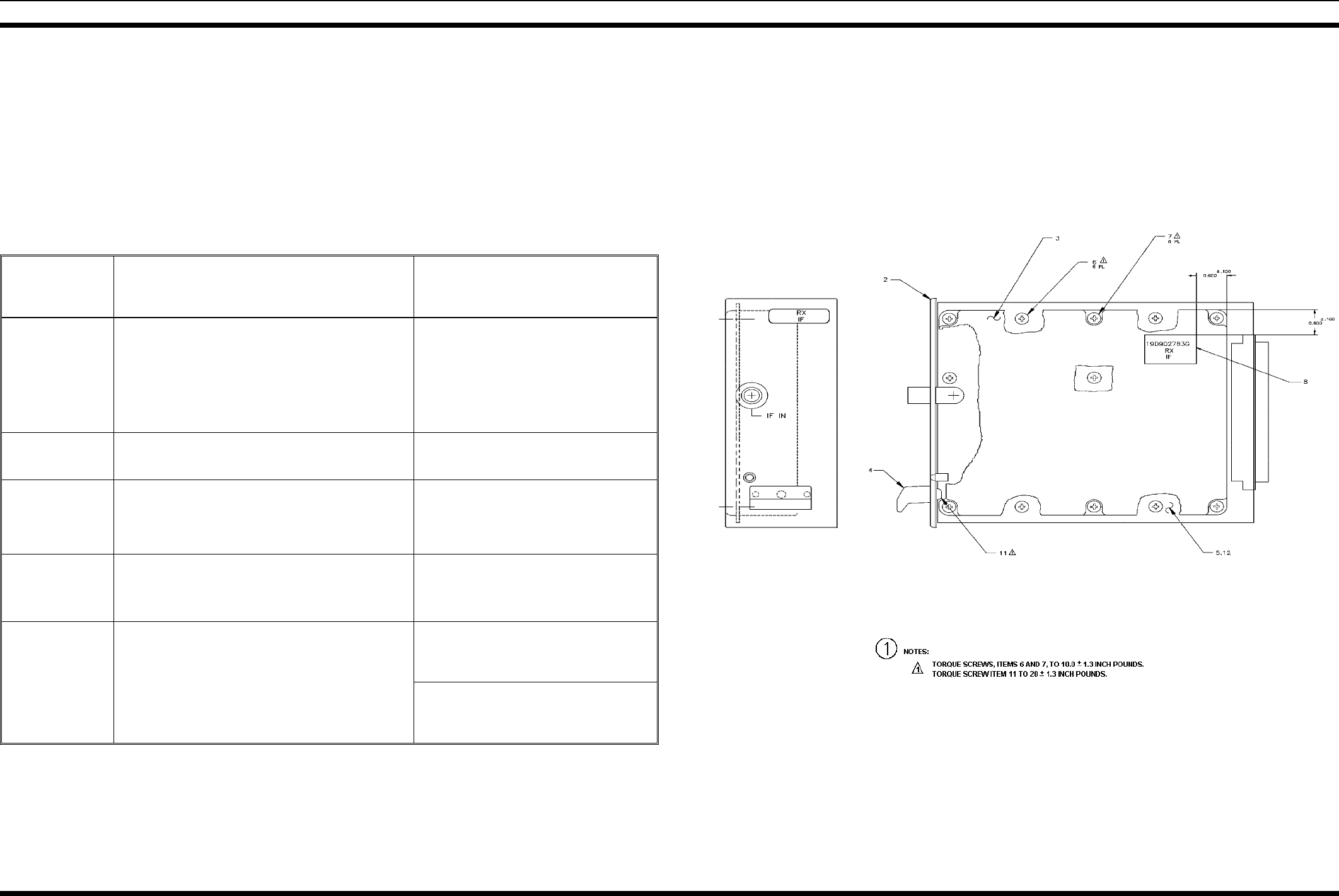
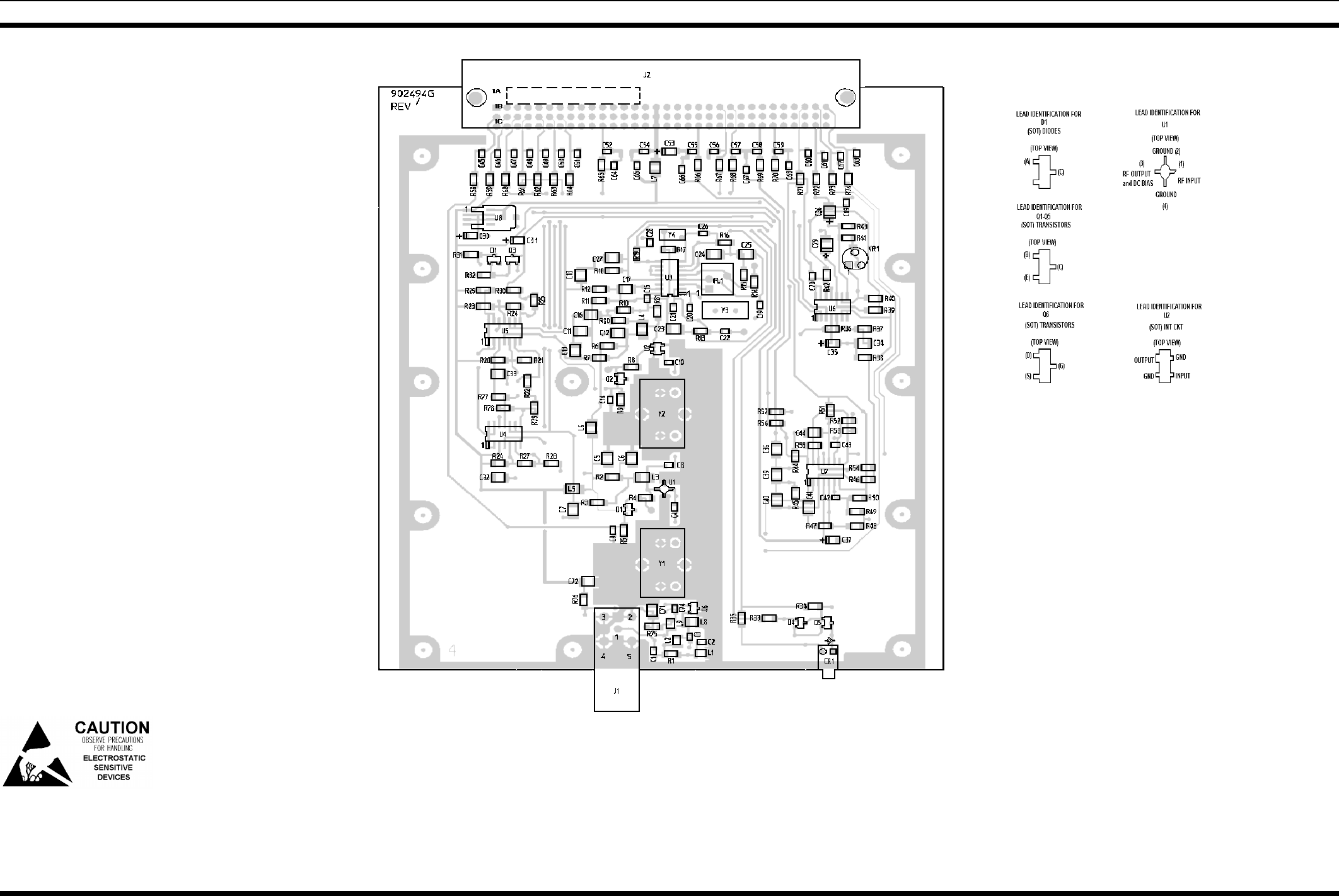
ASSEMBLY DIAGRAM
TROUBLE SHOOTING GUIDE
SYMPTOM CHECK
(CORRECT READING SHOWN) INCORRECT READING
INDICATES DEFECTIVE
COMPONENT
Fault indicator on Check DC voltages
+8V at U8 Pin 1
+4v at U Pin 7
5.5V at U1 output pin
3.3V at 2 output pin
4.4V at U3 Pin 4
If DC voltages not correct
U8 or associated components
U6 or associated components
U1 or associated components
U2 or associated components
U3 or associated components
If DC voltages correct
U4, U5, U6, D1, Q3, Q4, Q5
No audio - no
noise With no signal applied to module IF input
Check for AF noise @ C29 ; 200mV
Check for AF noise @ U6 Pin 8: 1 V U3 or associated components
U6 or associated components
Noise only - no
demodulated audio Check crystal oscillator: TP3 50 mVpk 20.945 MHz
Apply -30 dBm 21.4 MHz input, check TP1 100 mVpk
Apply -50 dBm 21.4 MHz input, check TP2 100 mVpk
Apply -60 dBm 21.4 MHz input, check TP4 100 mVpk
U3, Y3 or associated components
Q6, Y1, U1 or associated components
U2, Y2 or associated components
U3, FL1 or associated components
Poor 12 dB SINAD Check crystal oscillator: TP3 50 mVpk 20.945 MHz U3, Y3 or associated components
Apply -30 dBm 21.4 MHz input, check TP1 100 mVpk
Apply -50 dBm 21.4 MHz input, check TP2 100 mVpk
Apply -60 dBm 21.4 MHz input, check TP4 100 mVpk
Q6, Y1, U1 or associated components
U2, Y2 or associated components
U3, FL1 or associated components
No squelch
function With squelch pot maximum, or with module AUDIO/
SQUELCH/HI connected to SQUELCH/ARM input
and with no signal to module IF input:
Check Presence of 1 Vpk noise at U6 Pin 14 U6 or associated components
Check presence of 1 Vpk noise U7 at Pin 1
Check presence of 1 Vpk noise U7 Pin 1
Check DC voltage U7 at Pin 8: 7 V
Check DC voltage U7 Pin 14: 0.5 V U7 or associated components
RECEIVER IF MODULE
19D902783G1
(19D902783, Sh. 1, Rev. 3)
LBI-38643C
3
RECEIVER IF MODULE
19D902494G1
OUTLINE DIAGRAM
(19D902494, Sh. 1, Rev. 5B)
(19D902493, Comp. Side, Rev. 5)
LBI-38643C
4
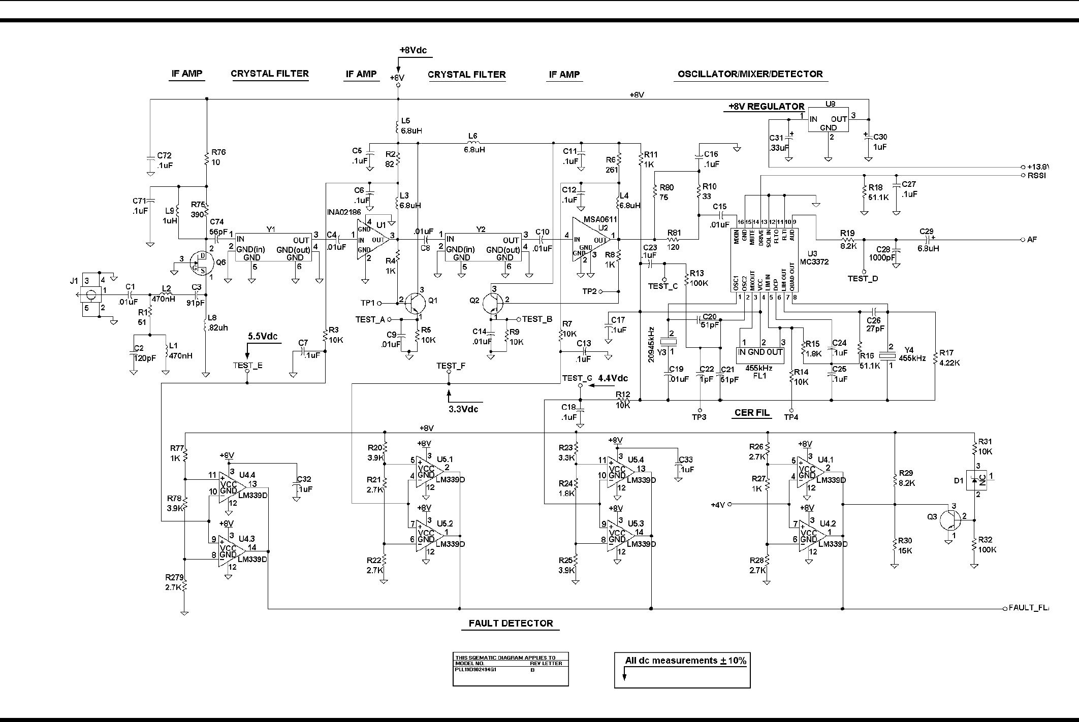
SCHEMATIC DIAGRAM
RECEIVER IF MODULE
19D902494G1
(19D902504, Sh. 1, Rev. 6)
LBI-38643C
5
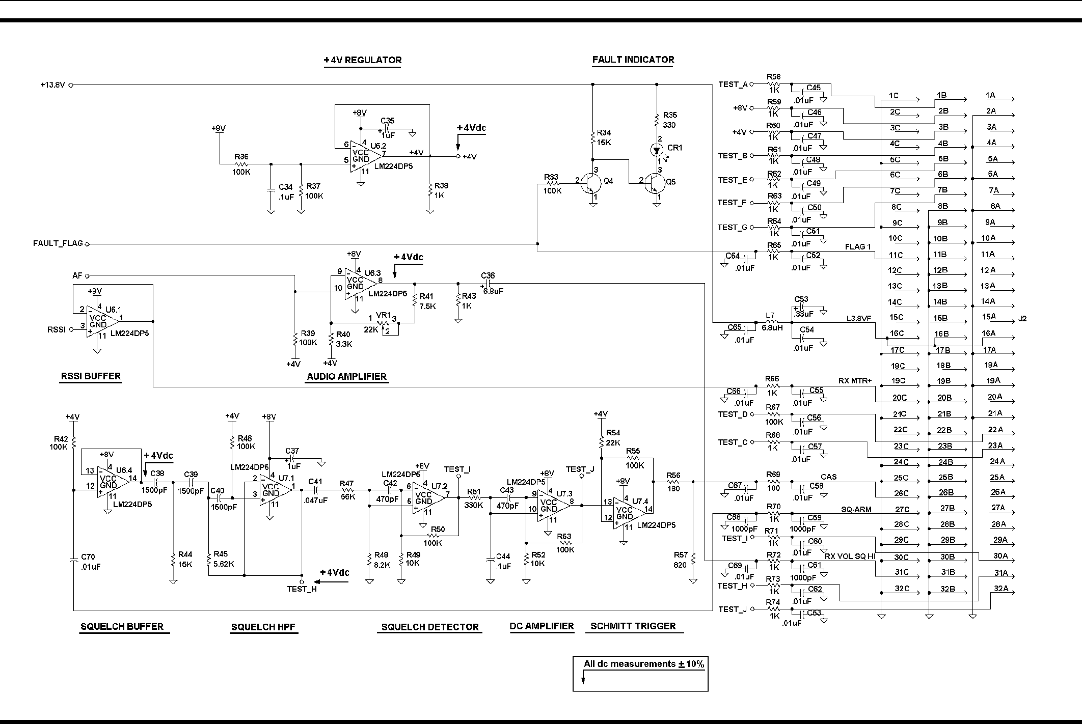
SCHEMATIC DIAGRAM
RECEIVER IF MODULE
19D902494G1
(19D902504, Sh. 2, Rev. 6)
LBI-38643C
6
PARTS LIST
SYMBOL PART NO. DESCRIPTION
R39 19B800607P104 Metal film: 100K ohms ±5%, 1/8 w.
R40 19B800607P332 Metal film: 3.3K ohms ±5%, 1/8 w.
R41 19A702931P285 Metal film: 7500 ohms ±1%, 200 VDCW, 1/8
w.
R42 19B800607P104 Metal film: 100K ohms ±5%, 1/8 w.
R43 19B800607P102 Metal film: 1K ohms ±5%, 1/8 w.
R44 19B800607P153 Metal film: 15K ohms ±5%, 1/8 w.
R45 19A702931P273 Metal film: 5620 ohms ±1%, 200 VDCW, 1/8
w.
R46 19B800607P104 Metal film: 100K ohms ±5%, 1/8 w.
R47 19B800607P563 Metal film: 68K ohms ±5%, 1/8 w.
R48 19B800607P822 Metal film: 8.2K ohms ±5%, 1/8 w.
R49 19B800607P103 Metal film: 10K ohms ±5%, 1/8 w.
R50 19B800607P104 Metal film: 100K ohms ±5%, 1/8 w.
R51 19B800607P334 Metal film: 330K ohms ±5%, 1/8 w.
R52 19B800607P103 Metal film: 10K ohms ±5%, 1/8 w.
R53 19B800607P104 Metal film: 100K ohms ±5%, 1/8 w.
R54 19B800607P223 Metal film: 22K ohms ±5%, 1/8 w.
R55 19B800607P104 Metal film: 100K ohms ±5%, 1/8 w.
R56 19B800607P181 Metal film: 180 ohms ±5%, 1/8 w.
R57 19B800607P821 Metal film: 820 ohms ±5%, 1/8 w.
R58
thru
R66
19B800607P102 Metal film: 1K ohms ±5%, 1/8 w.
R67 19B800607P104 Metal film: 100K ohms ±5%, 1/8 w
R68 19B800607P102 Metal film: 1K ohms ±5%, 1/8 w.
R69 19B800607P101 Metal film: 100 ohms ±5%, 1/8 w.
R70
thru
R74
19B800607P102 Metal film: 1K ohms ±5%, 1/8 w.
R75 19B800607P391 Metal film: 390 ohms ±5%, 1/8 w.
R76 19B800607P100 Metal film: 10 ohms ±5%, 1/8 w.
R77 19B800607P102 Metal film: 1K ohms ±5%, 1/8 w.
R78 19B800607P392 Metal film: 3.9K ohms ±5%, 1/8 w.
R79 19B800607P272 Metal film: 2.7K ohms ±5%, 1/8 w.
R80 19B800607P750 Metal film: 75 ohms ±5%, 1/8 w.
R81 19B800607P121 Metal film: 120 ohms ±5%, 1/8 w.
- - - - - -INTEGRATED CIRCUITS - - - - - -
U1 344A3740P1 Silicon, bipolar.
U2 19A705927P1 Silicon, bipolar.
U3 19A149980P2 Linear: Osc./Mixer/IF/Det./Amp.; sim to
MC3372D.
U4
and
U5
19A704125P1 Linear: Quad Comparator; sim to LM339D.
U6
and
U7
19A701789P5 Linear:Quad Op Amp; sim to LM224D.
U8 19A704971P10 Voltage regulator: 8 Vdc; sim to
MC78M08CDT.
- - - - - - - - VARIABLE RESISTOR - - - - - -
VR1 19B800779P12 Variable resistor: 22k ohms, 0.1 w; sim to
Murata RGV4E223.
*COMPONENTS, ADDED, DELETED OR CHANGED BY PRODUCTION CHANGES
VHF RECEIVER RF MODULE
19D902783G1
ISSUE 2
SYMBOL PART NO. DESCRIPTION
- - - - - MISCELLANEOUS - - - -
2 19D902508P1 Chassis.
3 19D902509P1 Cover.
4 19D902555P1 Handle.
6 19A702381P506 Screw, thread forming: TORX, No. M3.5 - 0.6
X 6.
7 19A702381P513 Screw, thread forming: TORX, No. M3.5 - 0.6
X 13.
11 19A702381P508 Screw, thread forming: No. 3.5-0.6 x 8.
Receiver IF Board
19D902494G1
- - - - - - - - - CAPACITORS - - - - - - - - - - -
C1 19A702052P14 Ceramic: 0.01 µF ±10%, 50 VDCW.
C2 19A702236P52 Ceramic: 120 pF, ±5%, 50 VDCW.
C3 19A702236P49 Ceramic: 91 pF, ±5%, 50 VDCW.
C4 19A702052P14 Ceramic: 0.01 µF ±10%, 50 VDCW.
C5
thru
C7
19A702052P26 Ceramic: 0.1 µF ±10%, 50 VDCW.
C8
thru
C10
19A702052P14 Ceramic: 0.01 µF ±10%, 50 VDCW.
C11
thru
C13
19A702052P26 Ceramic: 0.1 µF ±10%, 50 VDCW.
C14
and
C15
19A702052P14 Ceramic: 0.01 µF ±10%, 50 VDCW.
C16
thru
C18
19A702052P26 Ceramic: 0.1 µF ±10%, 50 VDCW.
C19 19A702052P14 Ceramic: 0.01 µF ±10%, 50 VDCW.
C20
and
C21
19A702061P47 Ceramic: 51 pF ±5%, 50 VDCW, temp coef 0
±30 PPM.
C22 19A702061P1 Ceramic: 1 pF ±0.5 pF, 50 VDCW.
C23
thru
C25
19A702052P26 Ceramic: 0.1 µF ±10%, 50 VDCW.
C26 19A702061P33 Ceramic: 27 pF ±5%, 50 VDCW, temp coef 0
±30 PPM/°C.
C27 19A702052P26 Ceramic: 0.1 µF ±10%, 50 VDCW.
C28 19A702052P5 Ceramic: 1000 pF ±10%, 50 VDCW.
C29 19A705205P5 Tantalum: 6.8 µF, 10 VDCW; sim to Sprague
293D.
C30 19A705205P2 Tantalum: 1 µF, 16 VDCW; sim to Sprague
293D.
C31 19A705205P12 Tantalum: .33 µF, 16 VDCW; sim to
Sprague 293D.
C32
thru
C34
19A702052P26 Ceramic: 0.1 µF ±10%, 50 VDCW
SYMBOL PART NO. DESCRIPTION
C35 19A705205P2 Tantalum: 1 µF, 16 VDCW; sim to Sprague 293D.
C36 19A705205P5 Tantalum: 6.8 µF, 10 VDCW; sim to Sprague
293D.
C37 19A705205P2 Tantalum: 1 µF, 16 VDCW; sim to Sprague 293D.
C38
thru
C40
19A702061P89 Ceramic: 1500 pF ±5%, 50 VDCW, temp coef 0
±30 PPM.
C41 19A702052P22 Ceramic: 0.047 µF ±10%, 50 VDCW.
C42
and
C43
19A702061P77 Ceramic: 470 pF ±5%, 50 VDCW, temp coef 0
±30 PPM.
C44 19A702052P26 Ceramic: 0.1 µF ±10%, 50 VDCW.
C45
thru
C52
19A702052P14 Ceramic: 0.01 µF ±10%, 50 VDCW.
C53 19A705205P12 Tantalum: .33 µF, 16 VDCW; sim to Sprague
293D.
C54
thru
C58
19A702052P14 Ceramic: 0.01 µF ±10%, 50 VDCW.
C59 19A702052P5 Ceramic: 1000 pF ±10%, 50 VDCW.
C60 19A702052P14 Ceramic: 0.01 µF ±10%, 50 VDCW.
C61 19A702052P5 Ceramic: 1000 pF ±10%, 50 VDCW.
C62
thru
C67
19A702052P14 Ceramic: 0.01 µF ±10%, 50 VDCW.
C68 19A702052P5 Ceramic: 1000 pF ±10%, 50 VDCW.
C69
and
C70
19A702052P14 Ceramic: 0.01 µF ±10%, 50 VDCW.
C71
and
C72
19A702052P26 Ceramic: 0.1 µF ±10%, 50 VDCW.
C74 19A702061P49 Ceramic: 56 pF ±5%, 50 VDCW, temp coef 0
±30 PPM.
- - - - - - - - - - - - DIODES - - - - - - - - - - - -
CR1 19A703595P10 Optoelectronic: Red LED in right angle housing;
sim to HP HLMP-1301-010.
D1 19A700083P105 Zener: 8.2V; sim to BZX84-C8V2.
- - - - - - - - - - - FILTERS - - - - - - - - - - - -
FL1 19A702171P3 Bandpass Filter: Fc = 455 kHz, 6dB BW = ±7.5
kHz; sim to Murata CFU455E2.
J1 19A115938P24 Connector, receptacle.
- - - - - - - - - - - JACKS - - - - - - - - - - - - -
J2 19B801587P7 Connector, DIN: 96 male contacts, right angle
mounting; sim to AMP 650887-1.
- - - - - - - - - - -INDUCTORS - - - - - - - - - - -
L1
and
L2
19A700021P13 Coil, fixed: 470 nH.
L3
thru
L7
19A705470P35 Coil, fixed: 6.8 µH.
L8 19A705470P24 Coil, fixed: 820 nH.
L9 19A700021P17 Coil, fixed: 1 µH.
SYMBOL PART NO. DESCRIPTION
- - - - - - - - TRANSISTORS - - - - - - - - -
Q1
and
Q2
19A704708P2 Silicon, NPN: sim to NEC 2SC3356.
Q3
thru Q5 19A700076P2 Silicon, NPN: sim to MMBT3904, low profile.
Q6 19A702524P2 N-Type, field effect.
- - - - - - - - - RESISTORS - - - - - - - - - - -
R1 19B800607P510 Metal film: 51 ohms ±5%, 1/8 w.
R2 19B800607P820 Metal film: 82 ohms ±5%, 1/8 w.
R3 19B800607P103 Metal film: 10K ohms ±5%, 1/8 w.
R4 19B800607P102 Metal film: 1K ohms ±5%, 1/8 w.
R5 19B800607P103 Metal film: 10K ohms ±5%, 1/8 w.
R6 19A702931P141 Metal film: 261 ohms ±1%, 200 VDCW,
1/8 w.
R7 19B800607P103 Metal film: 10K ohms ±5%, 1/8 w.
R8 19B800607P102 Metal film: 1K ohms ±5%, 1/8 w.
R9 19B800607P103 Metal film: 10K ohms ±5%, 1/8 w.
R10 19B800607P330 Metal film: 33 ohms ±5%, 1/8 w.
R11 19B800607P102 Metal film: 1K ohms ±5%, 1/8 w.
R12 19B800607P103 Metal film: 10K ohms ±5%, 1/8 w.
R13 19B800607P104 Metal film: 100K ohms ±5%, 1/8 w.
R14 19B800607P103 Metal film: 10K ohms ±5%, 1/8 w.
R15 19B800607P182 Metal film: 1.8K ohms ±5%, 1/8 w.
R16 19A702931P369 Metal film: 51.1K ohms ±1%, 200 VDCW, 1/8
w.
R17 19A702931P261 Metal film: 4220 ohms ±1%, 200 VDCW, 1/8
w.
R18 19A702931P369 Metal film: 51.1K ohms ±1%, 200 VDCW, 1/8
w.
R19 19B800607P822 Metal film: 8.2K ohms ±5%, 1/8 w.
R20 19B800607P392 Metal film: 3.9K ohms ±5%, 1/8 w.
R21
and
R22
19B800607P272 Metal film: 2.7K ohms ±5%, 1/8 w.
R23 19B800607P332 Metal film: 3.3K ohms ±5%, 1/8 w.
R24 19B800607P182 Metal film: 1.8K ohms ±5%, 1/8 w.
R25 19B800607P392 Metal film: 3.9K ohms ±5%, 1/8 w.
R26 19B800607P272 Metal film: 2.7K ohms ±5%, 1/8 w.
R27 19B800607P102 Metal film: 1K ohms ±5%, 1/8 w.
R28 19B800607P272 Metal film: 2.7K ohms ±5%, 1/8 w.
R29 19B800607P822 Metal film: 8.2K ohms ±5%, 1/8 w.
R30 19B800607P153 Metal film: 15K ohms ±5%, 1/8 w.
R31 19B800607P103 Metal film: 10K ohms ±5%, 1/8 w.
R32
and
R33
19B800607P104 Metal film: 100K ohms ±5%, 1/8 w.
R34 19B800607P153 Metal film: 15K ohms ±5%, 1/8 w.
R35 19B800607P331 Metal film: 330 ohms ±5%, 1/8 w.
R36
and
R37
19B800607P104 Metal film: 100K ohms ±5%, 1/8 w.
R38 19B800607P102 Metal film: 1K ohms ±5%, 1/8 w.
LBI-38643C
7
PARTS LIST & PRODUCTION CHANGES
PRODUCTION CHANGES
Changes in the equipment to improve performance or to simplify circuits are
identified by a "Revision Letter" which is stamped after the model number of the
unit. The revision stamped on the unit includes all previous revisions. Refer to
the Parts List for the descriptions of parts affected by these revisions.
Rev. A - 19D902494G1, 25 kHz IF Module Board
To improve performance in high temperature environments and to
eliminate Audio Level drifting, changed voltage regulator U8 and vari-
able resistor VR1.
U8 was: 19A704971P11, 8 Vdc; sim to MC78L08ACD.
VR1 was: 19A705496P5 20K ohms 0.1w; sim to Murata RGV4E203.
Rev. B - 19D902494G1, 25 kHz IF Module Board
To change Squelch Driver operation to allow compatibility with GETC,
changed resistors R56, R57, and R69.
R56 was: 19B800607P182 Metal film: 1.8K ohms ±5%, 1/8 w.
R57 was: 19B800607P822 Metal film: 8.2K ohms ±5%, 1/8 w.
R69 was: 19B800607P102 Metal film: 1K ohms ±5%, 1/8 w.
SYMBOL PART NO. DESCRIPTION
- - - - - - - - - - -CRYSTALS - - - - - - - - -
Y1 19A149974G7 Filter, crystal: Fc = 21.4 MHz, 3 dB BW =
15.0 kHz. Insertion loss = 2.0 dB max.
Y2 19A149974G8 Filter, crystal: Fc = 21.4 MHz, 3 dB BW =
15.0 kHz. Insertion loss = 3.0 dB max.
Y3 19A702284G5 Quartz crystal unit: 20.945000 MHz ±10 ppm
@ 25°C.
Y4 19A149976P1 Fixed: 455 kHz.
LBI-38643C
8
IC DATA
U4 & U5
19A704125P1
Quad Comparator
U6 & U7
19A701789P4
Quad Op-Amp
U8
19A704971P10
Voltage Regulator
U3
19A149980P2
FM Receiver
U1
344A3740P1
Silicon Bipolar IC
U2
19A705927P1
Silicon Bipolar IC
LBI-38643C
9
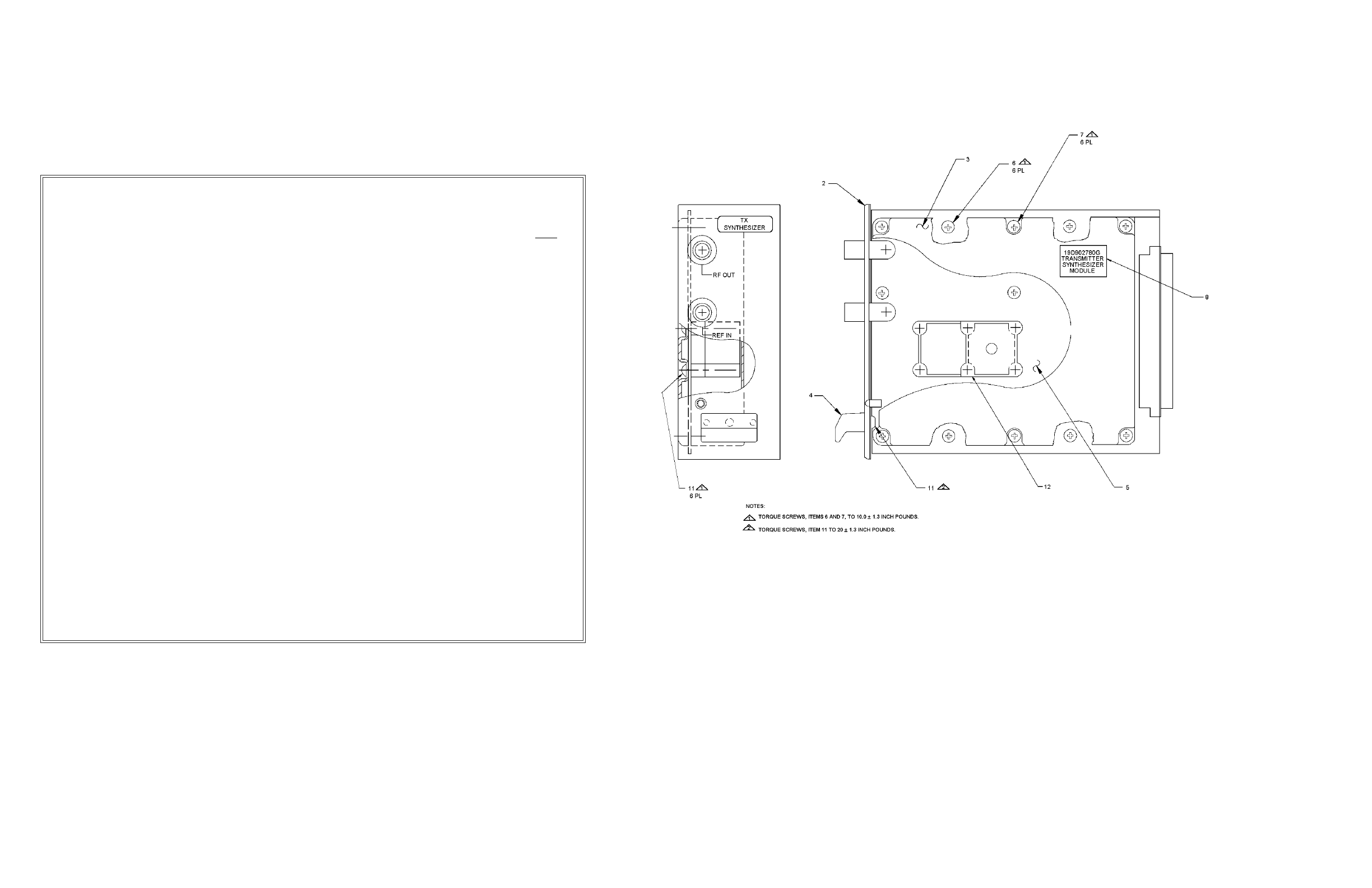
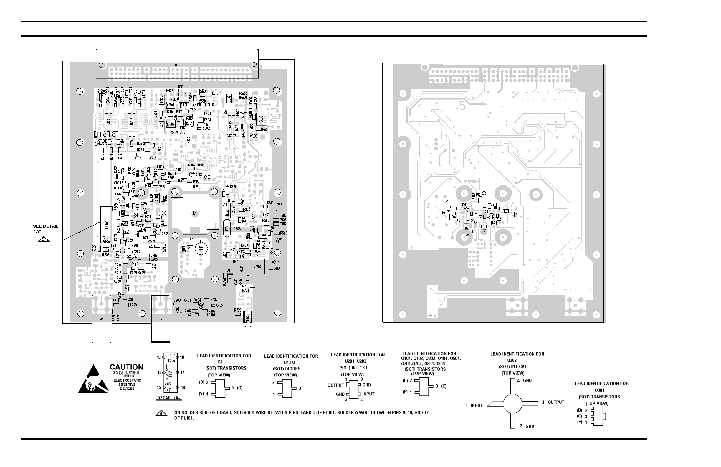
ASSEMBLY DIAGRAM
MAINTENANCE MANUAL
FOR
UHF TRANSMITTER SYNTHESIZER MODULE
19D902780G3, G6 - G10
LBI-38671H
TABLE OF CONTENTS
Page
DESCRIPTION . . . . . . . . . . . . . . . . . . . . . . . . . . . . . . . . . . . . . . . . . . . . . 1
GENERAL SPECIFICATIONS . . . . . . . . . . . . . . . . . . . . . . . . . . . . . . . . . . . . . 1
CIRCUIT ANALYSIS . . . . . . . . . . . . . . . . . . . . . . . . . . . . . . . . . . . . . . . . . . 1
VOLTAGE CONTROLLED OSCILLATOR . . . . . . . . . . . . . . . . . . . . . . . . . . . 1
FREQUENCY DOUBLER . . . . . . . . . . . . . . . . . . . . . . . . . . . . . . . . . . . . . 1
RF AMPLIFIERS . . . . . . . . . . . . . . . . . . . . . . . . . . . . . . . . . . . . . . . . . . 1
REFERENCE BUFFER AMPLIFIER . . . . . . . . . . . . . . . . . . . . . . . . . . . . . . . 1
PRESCALER AND SYNTHESIZER . . . . . . . . . . . . . . . . . . . . . . . . . . . . . . . 2
LOOP BUFFER AMPLIFIERS . . . . . . . . . . . . . . . . . . . . . . . . . . . . . . . . . . 2
AUDIO FREQUENCY AMPLIFIER . . . . . . . . . . . . . . . . . . . . . . . . . . . . . . . 2
VOLTAGE REGULATORS . . . . . . . . . . . . . . . . . . . . . . . . . . . . . . . . . . . . 2
LOGIC CIRCUITS . . . . . . . . . . . . . . . . . . . . . . . . . . . . . . . . . . . . . . . . . 3
BLOCK DIAGRAM . . . . . . . . . . . . . . . . . . . . . . . . . . . . . . . . . . . . . . . . . . . 2
MAINTENANCE . . . . . . . . . . . . . . . . . . . . . . . . . . . . . . . . . . . . . . . . . . . . 3
TEST PROCEDURE . . . . . . . . . . . . . . . . . . . . . . . . . . . . . . . . . . . . . . . . 3
ALIGNMENT PROCEDURE . . . . . . . . . . . . . . . . . . . . . . . . . . . . . . . . . . . 3
TROUBLESHOOTING . . . . . . . . . . . . . . . . . . . . . . . . . . . . . . . . . . . . . . 3
PARTS LIST . . . . . . . . . . . . . . . . . . . . . . . . . . . . . . . . . . . . . . . . . . . . . . . 4
PRODUCTION CHANGES . . . . . . . . . . . . . . . . . . . . . . . . . . . . . . . . . . . . . . . 6
IC DATA . . . . . . . . . . . . . . . . . . . . . . . . . . . . . . . . . . . . . . . . . . . . . . . . . 6
OUTLINE DIAGRAM . . . . . . . . . . . . . . . . . . . . . . . . . . . . . . . . . . . . . . . . . 8
SCHEMATIC DIAGRAM . . . . . . . . . . . . . . . . . . . . . . . . . . . . . . . . . . . . . . . . 9
ASSEMBLY DIAGRAM . . . . . . . . . . . . . . . . . . . . . . . . . . . . . . . . . . . . . . . . Back Cover
Ericsson Inc.
Private Radio Systems
Mountain View Road
Lynchburg, Virginia 24502
1-800-528-7711 (Outside USA, 804-592-7711) Printed in U.S.A.
E
UHF TRANSMITTER
SYNTHESIZER MODULE
19D902780G3, G6 - G10
(19D902780, Sh. 1, Rev. 5)

DESCRIPTION
The principle function of the Transmitter Synthesizer Module
is to provide the RF excitation for input to the MASTR III
station power amplifier. The output of the synthesizer is a
frequency modulated signal at the desired frequency. The mod-
ule contains the following functional blocks:
•A voltage controlled oscillator.
•Frequency Doubler (Multiplier).
•A chain of integrated circuit RF Amplifiers.
•A reference buffer amplifier.
•Dual modulus prescaler and synthesizer integrated
circuits.
•Loop amplifiers and passive loop filter.
•An audio amplifier and a pre-modulation integrator.
•IC voltage regulators for +5 and -5 Vdc. A discrete
component regulator for +8 Vdc, and an Opera-
tional Amplifier regulator for +4 Vdc.
•Logic circuitry: address decoder, input signal gates,
and a lock indicator circuit.
CIRCUIT ANALYSIS
VOLTAGE CONTROLLED OSCILLATOR
Transistor Q1 and associated circuitry comprise a low noise
Voltage Controlled Oscillator (VCO). Inductor L1 and asso-
ciated capacitors form the oscillator resonant circuit (tank).
The noise characteristic of this oscillator is dependent on the
Q of this resonant circuit. The components used in the tank
are specified to have especially high Q. Diode D1 aids in
setting the bias point for low noise operation. (Any field
replacement of oscillator parts should use identical parts).
Variable Capacitor C10 sets the fixed capacitance in the tank,
and therefore sets the frequency range over which the oscil-
lator can be voltage tuned.
The oscillator frequency is voltage tuned by the signal ap-
plied through R5 and L5 to the two varicap diodes D2 and
D3. Additionally, audio modulation is applied as an AF
voltage to the two varicap diodes. This RF voltage varies the
oscillator frequency at an audio rate (i.e., it frequency modu-
lates the oscillator). Low frequency audio is applied along
with the varicap control voltage through R5 and L5 while
high frequency audio (MOD) is applied via C16.
Resistors R6 through R9 provide a two volt negative bias on
the varicap diodes.
Transistors Q101 and Q102 and associated circuitry form the
oscillator enable switch. This switch allows the station con-
trol circuitry to turn the VCO ON or OFF via the ANT_REL
line. Setting the ANT_REL line to a logic low causes Q102
to conduct. The five (5) volt output at Q102 collector
(OSCON) enables the fault indicator gates, U705-3 and
U705-4, and turns on Q101. Q101 starts to conduct, provid-
ing a ground path for Q1. This turns ON the VCO.
FREQUENCY DOUBLER
Transistors Q801 and Q802 form a buffer stage to drive
transistor multiplier Q803. The buffer isolates VCO Q1 from
loading effects which could degrade oscillator loaded Q and
hence noise performance. Transistor multiplier Q803 is
tuned to pass the second harmonic of the VCO output and
serves as a frequency doubler. Tank elements L802, C812-
C814 and L803 form a resonant circuit and matching net-
work to drive resistive splitter R201-R204.
RF AMPLIFIERS
The RF chain begins with resistive splitter R201-R204 and
R216-R218. The output of the splitter at R203 is attenuated
by 10 dB and provides impedance matching helical filter
FL201, which is tuned to pass the fundamental while reject-
ing harmonics by approximately 40 dB. The output of FL201
is fed thru resistive pad R205-R207 to MMIC Amplifier
U201 which operates in compression. U201 drives output
amplifier U202 into compression. The output amplifier is
followed by a bandpass filter (C208-C210, L203-L205) and
resistive attenuators (R210-R215). The final output at the
front panel BNC Connector (J2) is nominally 11.5 dBm, and
drives the station Power Amp.
The other output of the resistive splitter at R218 is attenuated
by 20 dB and drives buffer amp U203 into compression.
U203 drives the synthesizer prescaler providing a feedback
signal for the synthesizer phase locked loop.
REFERENCE BUFFER AMPLIFIER
Transistor Q401 and associated components comprise a buff-
er amplifier for the reference oscillator signal. (The reference
oscillator signal is produced by the receiver synthesizer
module of a MASTR III station.) The 0 dBm reference
oscillator signal is fed through the front panel BNC connec-
tor J1. Resistor R405 provides a 50 ohm load to the reference
oscillator. The output of the Reference Buffer Amplifier is
fed directly to the synthesizer integrated circuit. The output
level at TP9 is approximately 3 volts peak to peak.
Copyright © June 1992, Ericsson GE Mobile Communications, Inc.
TABLE 1 - GENERAL SPECIFICATIONS
ITEM SPECIFICATION
FREQUENCY RANGE 450-470 MHz (G3)
425-450 MHz (G7)
403-430 MHz (G6)
380-400 MHz (G8)
470-494 MHz (G9)
490-512 MHz (G10)
CHANNEL SPACING 6.25 kHz
RF POWER OUT (50 Ohm load) 10 to 13 dBm
(10 to 20 mW)
RF HARMONICS < -30 dBc
NON-HARMONIC SPURS
1 to 200 MHz < - 90 dBc
200 MHz to 1 GHz < - 60 dBc
CARRIER ATTACK TIME <25 mSec
REFERENCE INPUT
input level 0 dBm ±1.5dB
input impedance 50 Ohm
frequency 5 to 17.925 MHz (must be integer divisible by
channel spacing)
MODULATION SENSITIVITY 5 kHz peak dev/1 Vrms, Adjustable
AF INPUT IMPEDANCE 600 Ohm
AF RESPONSE
10 Hz ±1.5 dB
1000 Hz0 dB reference
3 kHz ±1.5 dB
10 Hz SQUARE WAVE MODULATION <10%
Sq wave droop
HUM & NOISE -55 dB
POWER REQUIREMENTS 13.8 Vdc @ 275 mA
-12.0 Vdc @ 10 mA
This manual is published by Ericsson Inc., without any warranty. Improvements and changes to this manual necessitated by typographical errors, inaccuracies of current information, or improvements to programs
and/or equipment, may be made by Ericsson Inc., at any time and without notice. Such changes will be incorporated into new editions of this manual. No part of this manual may be reproduced or transmitted in any
form or by any means, electronic or mechanical, including photocopying and recording, for any purpose, without the express written permission of Ericsson Inc.
LBI-38671H
1
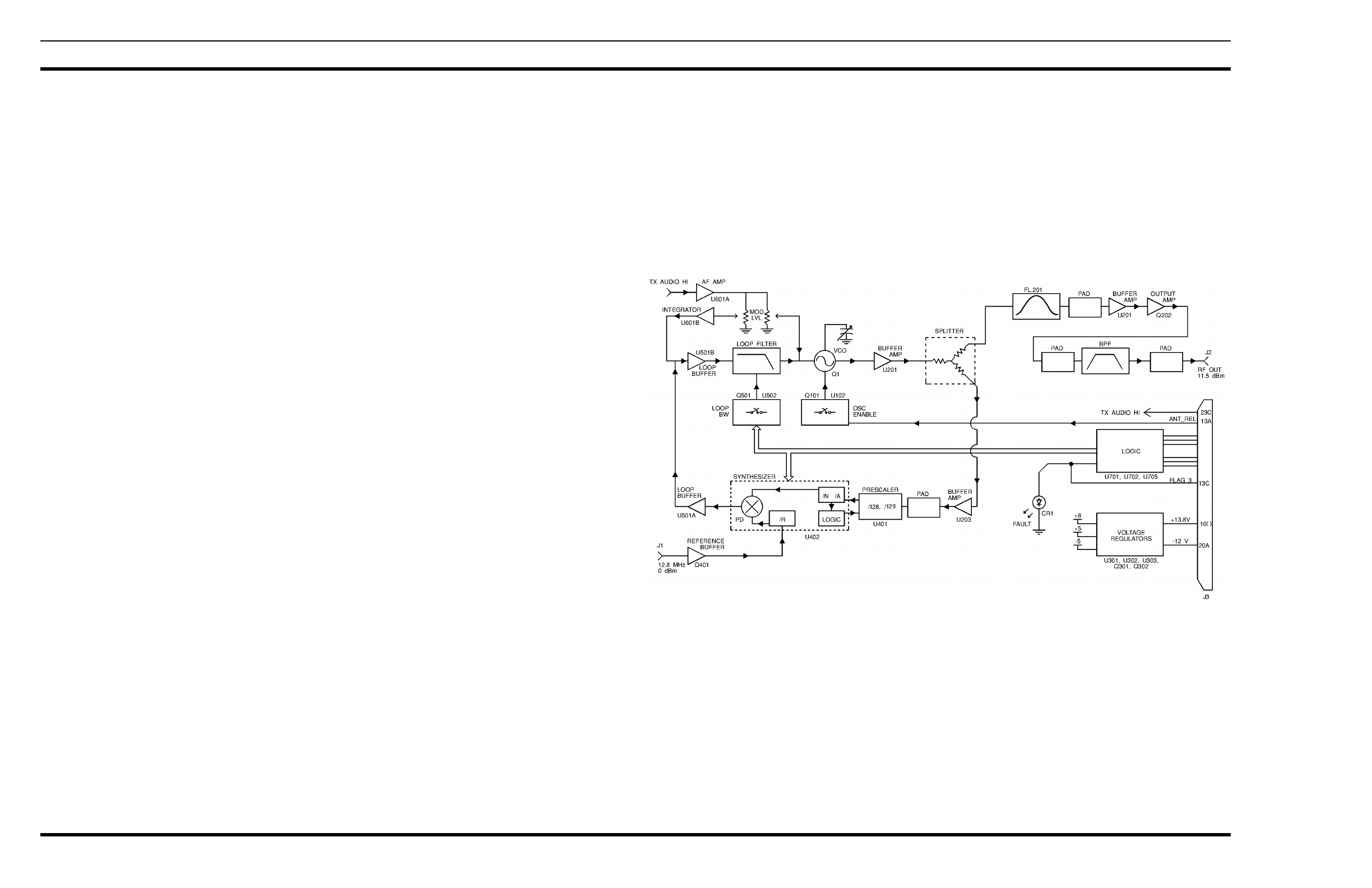
PRESCALER AND SYNTHESIZER
Integrated circuit U402 is the heart of the synthesizer. It
contains the necessary frequency dividers and control cir-
cuitry to synthesize output frequencies by the technique of
dual modulus prescaling. U402 also contains an analog
sample and hold phase detector and a lock detector circuit.
Within the synthesizer (U402) are three programmable di-
viders which are loaded serially using the CLOCK, DATA,
and ENABLE inputs (pins 11, 12, and 13 respectively). A
serial data stream (DATA) on pin 12 is shifted into internal
shift registers by low to high transitions on the clock input
(CLOCK) at pin 11. A logic high (ENABLE) on pin 13 then
transfers the program information from the shift registers to
the divider latches.
The reference signal is applied to U402 pin 2 and divided by
the "R" divider. This divides the reference signal down to a
divided reference frequency (Fr). The typical reference fre-
quency is 12.8 MHz and the typical divided reference fre-
quency is 6.25 kHz providing for synthesizer steps of 6.25
kHz for use with both 12.5 kHz and 25 kHz channel spacing.
Other channel spacings are possible by providing proper
programming.
The "A" and "N" dividers process the loop feedback signal
provided by the VCO (by way of the dual modulus prescaler
U401). The output of the "N" divider is a divided version of
the VCO output frequency (Fv).
Synthesizer U402 also contains logic circuitry to control the
dual modulus prescaler U401. If the locked synthesizer
output frequency is 450 MHz. The prescaler output nomi-
nally will be equal to 3.515625 MHz (450 MHz/128). This
frequency is further divided down to Fv by the "N" divider
in U402. Fv is then compared with Fr in the phase detector
section.
The phase detector output voltage is proportional to the
phase difference between Fv and Fr. This phase detector
output serves as the loop error signal. This error signal
voltage tunes the VCO to whatever frequency is required to
keep Fv and Fr locked (in phase).
LOOP BUFFER AMPLIFIERS AND LOOP
FILTER
The error signal provided by the phase detector output is
buffered by operational amplifiers (op-amp) U501A and
U501B. The audio modulation signal from U601B is also
applied to the input of U501B. The output of U501B is the
sum of the audio modulation and the buffered error signal.
The output of the second buffer (U501B) is applied to a loop
filter consisting of R506, R507, R508, C505 and C506. This
filter controls the bandwidth and stability of the synthesizer
loop. The UHF transmitter synthesizer has a loop bandwidth
of only several Hertz. This is very narrow, resulting in an
excessively long loop acquisition time. To speed acquisition,
switches U502A and U502C bypass the filter circuit when-
ever an ENABLE pulse is received by the Input Gates.
AUDIO FREQUENCY AMPLIFIER
The transmitter synthesizer audio input line is fed to U601A.
U601A is configured as a unity gain op-amp. Resistor R601
sets the 600 ohm input impedance of this amplifier. (NOTE:
Data for digital modulation is fed to the synthesizer through
the audio input line).
The amplifier output is split into two components and fed to
two variable resistors VR601 and VR602. VR601 sets the
level in the low frequency audio path and VR602 sets the
level in the high frequency audio path. (There is no clear
break between the low and high frequency ranges. All voice
frequencies are within the high frequency range. The low
frequency range contains low frequency data components).
The wiper of VR601 (low frequency path) connects to the
input of U601B, the pre-modulation integrator. U601B per-
forms the function of a low-pass filter and integrator. The
integrator output is summed with the PLL control voltage at
the input of loop buffer amplifier U501B. This integrated
audio signal phase modulates the VCO. The combination of
pre-integration and phase modulation is equivalent to fre-
quency modulation.
The wiper of VR602 (high frequency path) is connected to
the modulation input of the VCO through C16.
VOLTAGE REGULATORS
U301 and U303 are monolithic voltage regulators (+5 Vdc
and -5 Vdc respectively). These two voltages are used by
synthesizer circuitry. The +5 V regulator output is also used
as a voltage reference for the +8 Vdc discrete regulator
circuit.
U302A, Q302 and associated circuitry comprise the +8 volt
regulator. Most module circuitry is powered from the +8 volt
line. The regulator is optimized for especially low noise
performance. This is critical because the low noise VCO is
powered by the +8 volt line.
The +8 Vdc line also feeds the +4 Vdc regulator, U302B and
associated resistors. The +4 Vdc regulator provides a bias
voltage for several op-amps in the module.
Figure 1 - Block Diagram
LBI-38671H
2
LOGIC CIRCUITS
Logic circuitry (other than that inside the synthesizer IC -
U402) consists of the following:
•An address decoder
•Input gates and level shifters
•Lock Indicator circuitry
The address decoder, U702, enables the Input Gates when the
A0, A1, and A2 input lines receive the proper logic code (110
for the transmitter synthesizer). After receiving the proper
code, Y3 (U702-12) sends a logic low signal to U701C. U701C
acts as an inverter and uses the logic high output to turn on
Input Gates U701A, U701B, and U701D. The Input Gates
allow the clock, data and enable information to pass on to the
synthesizer via the level shifters. The Level Shifter Transistors
Q701, Q702 and Q703 convert the 5 volt gate logic level to the
8 volt logic level required by the synthesizer U402.
The Fault Indicator circuitry indicates when the synthesizer is
in an out-of-lock condition. The fault detector latches, U705A
and U705B are reset by the enable pulse during initial loading
of data into the synthesizer. If at any time afterwards the lock
detector signal (LD) goes low, the high output of U705B will
cause the output of gates U705C and U705D to go low. The
low output from U705C causes Q704 to conduct turning on the
front panel LED (CR701). The output of U705D (FLAG) is
connected to J3-13C for external monitoring of the Synthesizer
Module. A logic low on the FLAG line indicates an out-of-lock
condition.
MAINTENANCE
RECOMMENDED TEST EQUIPMENT
The following test equipment is required to test the synthesizer
Module:
1. RF signal source for 12.8 MHz, 0 dBm reference (in-
cluded with item 10)
2. AF Generator or Function Generator
3. Modulation Analyzer; HP 8901A, or equivalent, or a
UHF receiver
4. Oscilloscope; 20 MHz
5. DC Meter; 10 meg ohm (for troubleshooting)
6. Power Supply; 13.8 Vdc @ 350 mA
12.0 Vdc @ 25 mA
7. Spectrum Analyzer; 0-1 GHz
8. Frequency Counter; 10 MHz - 500 MHz
9. Personal Computer (IBM PC compatible) to load fre-
quency data
10. Service Parts Kit, (TQ-0650), (includes software for
loading frequency data)
TEST PROCEDURE
(Steps 5, 6, and 7 can be done using a modulation analyzer
or UHF receiver with 750 µs de-emphasis switchable in or
out.
1. Lock synthesizer at 470.0 (G3), 430 (G6), 450 (G7),
400 (G8), 494 (G9) or 512 (G10) MHz using software
provided in the service parts kit.
Verify lock (flag = high).
Verify front panel LED is off.
2. Measure output frequency.
Verify frequency = 470.0000 (G3), 425.000
(G6) or 450.000 (G7) MHz, 400.000 (G8),
494.000 (G9) or 512.000 (G10) ±200 Hz.
3. Measure harmonic content.
Verify 2nd harmonic is < -30 dBc.
4. Measure RF power output into 50 ohm load.
Verify 10 to 13 dBm (10 to 20 mW).
5. Measure AF distortion with standard modulating sig-
nal input.
Verify <2.5%.
6. Measure Hum and Noise relative to 0.44 kHz average
deviation, (de-emphasis on).
Verify < -55dB
7. Measure AF response at 300 Hz, 1 kHz (ref) and 3
kHz, (de-emphasis off).
Verify within ±1.5 dB with respect to 1 kHz
reference.
8. Verify lock at different frequencies.
a. Lock synthesizer at 380 (G8), 450 (G3), 403
(G6), 425 (G7), 470 (G9) or 492 (G10) MHz.
Verify LED is off.
b. Lock synthesizer at 385 (G8), 455 (G3), 408.5
(G6), 430 (G7), 476 (G9) or 497 (G10) MHz.
Verify LED is off.
c. Lock synthesizer at 395 (G8), 465 (G3), 419.5
(G6), 445 (G7), 488 (G9) or 507 (G10) MHz.
Verify LED is off.
d. Lock synthesizer at 400 (G8), 470 (G3), 425
(G6), 450 (G7), 494 (G9) or 512 (G10) MHz.
Verify LED is off.
ALIGNMENT PROCEDURE
1. Apply +13.8 Vdc and -12 Vdc. Verify the current
drain on the 13.8 volt supply is, <300mA and the
current drain on the -12 volt supply is <20 mA.
2. Lock the synthesizer at 380 (G8), 450 (G3), 403 (G6),
425 (G7), 470 (G9) or 492 (G10) MHz. Adjust trim-
mer C1O until Vtest (23A) reads 2.5 (G3, G8), 2.0
(G6, G7, G9) or 3.0 (G10) V ±0.05V.
3. Lock synthesizer at 460.0 (G3), 390.0 (G8), 414 (G6)
or 437.5 (G7), 482 (G9) or 502 (G10) MHz for the
following three adjustments.
•Set VR602 for 4.5 kHz peak deviation with a stand-
ard modulating signal applied to the audio input.
•Set VR601 for 4.5 kHz peak deviation with 1.0
Vrms, 10 Hz (or 7 Hz for G3) sine wave audio
applied to module AF input.
•Apply a 10 Hz 1.4 Vpk square wave to module AF
input. Adjust VR601 slightly for the flattest de-
modulated square wave using a modulation ana-
lyzer or receiver (no de-emphasis) and an
oscilloscope. The maximum net variation in voltage
over 1/2 cycle is 5%.
TROUBLESHOOTING
A troubleshooting guide is provided showing typical meas-
urements at the various test points.
This adjustment is critical for EDACS application
and must be reset at customer frequency.
NOTE
SERVICE NOTES
The following service information applies when
aligning, testing, or troubleshooting the TX Synthe-
sizer:
•Standard Modulating Signal = 1 kHz sinusoidal
voltage, 0.6 Vrms at the module input terminals
(600 ohm Rin).
•Logic Levels:
Logic 1 = high = 4.5 to 5.5 Vdc
Logic 0 = Low = 0 to 0.5 Vdc
•Transmitter Synthesizer Address = A0 A1 A2 =
110
•Synthesizer data input stream is as follows:
14-bit "R" divider most significant bit
(MSB) = R13 through "R" divider least sig-
nificant bit (LSB) = R0
10-bit "N" divider MSB = N9 through "N"
divider LSB = N0
7-bit "A" divider MSB = A6 through "A"
divider LSB = A0
Single high Control bit (last bit)
Latched When Control Bit = 1
DATA ENTRY FORMAT
Latched When
Control Bit = 1
Data in ➞Last A0 A6 N0 N9 R0 R13 ➞
Bit LSB – – – – – MSB LSB – – – – MSB LSB
For the transmitter synthesizer, 5 kHz chan-
nel spacing
R = 2560
N = integer part of (frequency in kHz)/(320)
A = (frequency in kHz)/(5) - 64*N
All numbers must be converted to binary.
•ANT_REL line must be logic low (0V) in order to
lock synthesizer.
•Synthesizer lock is indicated by the extinguishing
of the front panel LED indicator and a logic high
on the fault flag line (J3 pin 13C).
•Always verify synthesizer lock after each new data
loading.
Control B
LBI-38671H
3
PARTS LIST
SYMPTOM CHECK
(CORRECT READINGS SHOWN) INCORRECT READING INDICATES
DEFECTIVE COMPONENT
SYNTHESIZER FAILS TO LOCK Check DC voltages
+5 V @ U301 Pin 1
+8 V @ Q301 collector
-5 V @ U303 Pin 1
U301 or associated components
U302, Q301, Q302 or associated
components
U303 or associated components
Check 12.8 MHz reference signal
3V P-P, 12.8 MHz @ U402 Pin 2 No reference signal to front panel BNC or
Q401
Check oscillator signal
11.5 ±1.5 dBm 435 to 485 MHz at
front panel BNC
Proceed to "Low/No RF output" below
Check prescaler output
IV P-P, 3.5 MHz @ U401 Pin 4 U202, U401
Check CLOCK, DATA, ENABLE
While loading frequency data into
synthesizer Check 8V logic signals
@ Pins 11, 12, 13 of U402
Wrong address or
U701, U702, Q701, Q702, Q703
Check Phase detector output
6.25 kHz random signal @ U501
Pin 7 U402, U501
Low/No RF Output Check oscillator
LESS than 0.5 Vdc @ collector of
Q101 Synthesizer not keyed (low on ANT relay
line) or Q101, Q102
Check RF chain
No Modulation Check AF amplifier
Apply IV, 1 kHz signal to
TX/Audio/Hi U601
Check IV signal @ U601 Pin 1
TROUBLESHOOTING GUIDE UHF TRANSMITTER SYNTHESIZER MODULE
19D902780G3, G6 - G10
ISSUE 9
*COMPONENTS, ADDED, DELETED OR CHANGED BY PRODUCTION CHANGES
SYMBOL PART NO. DESCRIPTION
TRANSMITTER SYNTHESIZER BOARD
19D902779G3, G6 - G10
- - - - - - - - - MISCELLANEOUS - - - - - - - - -
2 19D902508P4 Chassis.
3 19D902509P2 Cover.
4 19D902555P1 Handle.
6 19A702381P506 Screw, thread forming: TORX, No. M3.5-.6 x 6.
7 19A702381P513 Screw, thread forming: TORX, No. M3.5 - 0.6 X 13.
11 19A702381P508 Screw, thd. form: No. 3.5-0.6 x 8.
12 19D902824P1 Casting.
- - - - - - - - - - CAPACITORS - - - - - - - - -
C1 19A702236P25 Ceramic: 10 pF + or -.5 pF, 50 VDCW, temp coef
+ or -30 PPM/°C.
C2 19A702236P32 Ceramic: 18 pF + or -5%, 50 VDCW, temp coef 0 +
+ or or -30 PPM
C3 19A702236P28 Ceramic: 12 pF + or - 5%, 50 VDCW, temp coef 0
+ or -30 PPM.
C4 19A702236P1 Ceramic: 0.5 pF + or - pF, temp coef 0
+ or - PPM/°C. (Used in G8).
C4 19A702236P8 Ceramic: 1.5 pF + or -.25 pF, 50 VDCW.
(Used in G3, G6, G7)
C4
and
C5
19A702236P17 Ceramic: 4.7 pF + or -0.5%, 50 VDCW, temp coef 0
+ or -60 PPM. (Used in G9).
C4 19A702236P11 Ceramic: 2.7 pF + or - .25 pF, 50 VDCW, temp coef 0
+ or -30 PPM/°C. (Used in G10).
C5 19A702236P17 Ceramic: 4.7 pF + or -5%, 50 VDCW, temp coef 0
+ or -30 PPM. (Used in G3 & G10).
C5 19A702236P17 Ceramic: 4.7 pF + or -5%, 50 VDCW, temp coef 0
+ or -30 PPM. (Used in G6 & G8).
C5 19A702236P15 Ceramic: 3.9 pF + or -.25 pF, 50 VDCW, temp
+ or -30 PPM/°C. (Used in G7).
C6 19A702236P28 Ceramic: 12 pF + or - 5%, 50 VDCW, temp coef 0
+ or -30 PPM. (Used in G8 & G3).
C6 19A702236P30 Ceramic: 15 pF + or -5%, 50 VDCW, temp coef 0 +
or -30 PPM/°C. (Used in G6 & G7).
*C6 19A702236P28 Ceramic: 12 pF + or -5%, 50 VDCW, temp coef 0
+ or -30 PPM/°C. (Used in G9 & G10).
C7 19A702061P99 Ceramic: 1000 pF + or -5%, 50 VDCW, temp coef 0
+ or -30 PPM/°C.
C8 19A702052P14 Ceramic: 0.01 uF + or - 10%, 50 VDCW.
C9 19A705205P6 Tantalum: 10 uF, 16 VDCW; sim to Sprague 293D.
C10 19A134227P5 Variable: 1.5 to 14 pF, 100 VDCW.
C11 19A705205P2 Tantalum: 1 uF, 16 VDCW; sim to Sprague 293D.
C12 19A702052P14 Ceramic: 0.01 uF + or - 10%, 50 VDCW.
C13 19A702061P99 Ceramic: 1000 pF + or -5%, 50 VDCW, temp coef 0
and + or -30 PPM/°C.
C14
*C15 19A700004P6 Metallized polyester: 4.7 uF + or - 10%, 63 VDCW.
*C16 19A702052P106 Ceramic: 1500 pF + or -5%, 50 VDCW.
C17 19A702061P99 Ceramic: 1000 pF + or -5%, 50 VDCW, temp coef 0
+ or -30 PPM/°C.
C18 19A705205P2 Tantalum: 1 uF, 16 VDCW; sim to Sprague 293D.
and
C19
C101 19A702061P99 Ceramic: 1000 pF + or -5%, 50 VDCW, temp coef 0
+ or -30 PPM/°C.
C102 19A705205P2 Tantalum: 1 uF, 16 VDCW; sim to Sprague 293D.
C103 19A702061P99 Ceramic: 1000 pF + or -5%, 50 VDCW, temp coef 0
+ or -30 PPM/°C.
SYMBOL PART NO. DESCRIPTION
C201 19A702061P61 Ceramic: 100 pF + or - 5%, 50 VDCW, temp coef 0
+ or - 30 PPM.
C202 19A702061P99 Ceramic: 1000 pF + or -5%, 50 VDCW, temp coef 0
+ or -30 PPM/°C.
C203 19A705205P2 Tantalum: 1 uF, 16 VDCW; sim to Sprague 293D.
C204 19A702061P61 Ceramic: 100 pF + or - 5%, 50 VDCW, temp coef 0
and + or - 30 PPM.
C205
C206 19A702061P99 Ceramic: 1000 pF + or -5%, 50 VDCW, temp coef 0
+ or -30 PPM/°C.
C207 19A705205P2 Tantalum: 1 uF, 16 VDCW; sim to Sprague 293D.
C208 19A702236P28 Ceramic: 12 pF + or - 5%, 50 VDCW, temp coef 0
+ or -30 PPM.
C209 19A702236P10 Ceramic: 2.2 pF + or -2.5 pF, 50 VDCW, temp
+ or -30 PPM/°C. (Used in G3, G6, G7, G8).
C209 19A702236P8 Ceramic: 1.5 pF + or -0.25 pF, 50 VDCW, temp
+ or -30 PPM/°C. (Used in G9 & G10).
C210 19A702236P28 Ceramic: 12 pF + or - 5%, 50 VDCW, temp coef 0
+ or -30 PPM.
C211 19A702061P61 Ceramic: 100 pF + or - 5%, 50 VDCW, temp coef 0
and + or - 30 PPM.
C212
C213 19A705205P2 Tantalum: 1 uF, 16 VDCW; sim to Sprague 293D.
C214 19A702061P99 Ceramic: 1000 pF + or -5%, 50 VDCW, temp coef 0
+ or -30 PPM/°C.
C215 19A702061P61 Ceramic: 100 pF + or - 5%, 50 VDCW, temp coef 0
+ or - 30 PPM.
C301 19A702061P99 Ceramic: 1000 pF + or -5%, 50 VDCW, temp coef 0
+ or -30 PPM/°C.
C302 19A702052P14 Ceramic: 0.01 uF + or - 10%, 50 VDCW.
C303 19A705205P2 Tantalum: 1 uF, 16 VDCW; sim to Sprague 293D.
and
C304
C305 19A705205P7 Tantalum: 10 uF, 25 VDCW; sim to Sprague 293D.
C306 19A705205P2 Tantalum: 1 uF, 16 VDCW; sim to Sprague 293D.
C307 19A705205P6 Tantalum: 10 uF, 16 VDCW; sim to Sprague 293D.
C308 19A702061P99 Ceramic: 1000 pF + or -5%, 50 VDCW, temp coef 0
and + or -30 PPM/°C.
C309
C310 19A705205P6 Tantalum: 10 uF, 16 VDCW; sim to Sprague 293D.
C311 19A705205P2 Tantalum: 1 uF, 16 VDCW; sim to Sprague 293D.
C312 19A702061P99 Ceramic: 1000 pF + or -5%, 50 VDCW, temp coef 0
+ or -30 PPM/°C.
C313 19A705205P6 Tantalum: 10 uF, 16 VDCW; sim to Sprague 293D.
C401 19A702052P14 Ceramic: 0.01 uF + or - 10%, 50 VDCW.
C402 19A702061P99 Ceramic: 1000 pF + or -5%, 50 VDCW, temp coef 0
+ or -30 PPM/°C.
C403 19A702052P14 Ceramic: 0.01 uF + or - 10%, 50 VDCW.
thru
C405
C406 19A702061P99 Ceramic: 1000 pF + or -5%, 50 VDCW, temp coef 0
+ or -30 PPM/°C.
C407 19A702052P14 Ceramic: 0.01 uF + or - 10%, 50 VDCW.
C408 19A702061P99 Ceramic: 1000 pF + or -5%, 50 VDCW, temp coef 0
+ or -30 PPM/°C.
C409 19A705205P6 Tantalum: 10 uF, 16 VDCW; sim to Sprague 293D.
C410 19A702052P26 Ceramic: 0.1uF + or - 10%, 50 VDCW
C411 19A705205P6 Tantalum: 10 uF, 16 VDCW; sim to Sprague 293D.
C412 19A702052P14 Ceramic: 0.01 uF + or - 10%, 50 VDCW.
C413 19A702052P108 Ceramic: 0.01 uF + or -10%, 50 VDCW.
C414 19A702061P69 Ceramic: 220 pF + or -5%, 50 VDCW, temp coef 0
+ or -30 PPM/°C.
C501 19A705205P2 Tantalum: 1 uF, 16 VDCW; sim to Sprague 293D.
C502 19A705205P2 Tantalum: 1 uF, 16 VDCW; sim to Sprague 293D.
C503 19A702052P33 Ceramic: 0.1 uF + or -10%, 50 VDCW.
LBI-38671H
4
PARTS LIST
SYMBOL PART NO. DESCRIPTION
C504 19A702061P99 Ceramic: 1000 pF + or -5%, 50 VDCW, temp coef 0
+ or -30 PPM/°C.
C505 19A703684P3 Metalized polyester: 2.2 uF + or - 10$, 50 VDCW.
C506 19A703902P3 Metal: 0.047 uF + or -10%, 50 VDCW.
C507 19A702052P33 Ceramic: 0.1 uF + or -10%, 50 VDCW.
C602 19A705205P6 Tantalum: 10 uF, 16 VDCW; sim to Sprague 293D.
C603 19A702061P99 Ceramic: 1000 pF + or -5%, 50 VDCW, temp coef 0
+ or -30 PPM/°C.
C604 19A705205P2 Tantalum: 1 uF, 16 VDCW; sim to Sprague 293D.
C605 19A703684P3 Metalized polyester: 2.2 uF + or - 10$, 50 VDCW.
C701 19A702061P61 Ceramic: 100 pF + or - 5%, 50 VDCW, temp coef 0
thru + or - 30 PPM.
C712
C714 19A702061P99 Ceramic: 1000 pF + or -5%, 50 VDCW, temp coef 0
and + or -30 PPM/°C.
C715
C801 19A702061P4 Ceramic: 1.8 pF + or - 0.5 pF, 50 VDCW, temp
or - 250 PPM.
C802 19A705205P6 Tantalum: 10 uF, 16 VDCW; sim to Sprague 293D.
C803 19A702052P14 Ceramic: 0.01 uF + or - 10%, 50 VDCW.
and
C804
C805 19A702061P99 Ceramic: 1000 pF + or -5%, 50 VDCW, temp coef 0
+ or -30 PPM/°C.
C806 19A702061P65 Ceramic: 150 pF + or -5%, 50 VDCW, temp coef 0
+ or -30 PPM/°C.
C807 19A705205P6 Tantalum: 10 uF, 16 VDCW; sim to Sprague 293D.
C808 19A702052P14 Ceramic: 0.01 uF + or - 10%, 50 VDCW.
C809 19A702061P13 Ceramic: 10 pF + or - 5%, 50 VDCW, temp coef 0
+ or - 30 PPM.
C810 19A702052P14 Ceramic: 0.01 uF + or - 10%, 50 VDCW.
C811 19A702061P99 Ceramic: 1000 pF + or -5%, 50 VDCW, temp coef 0
+ or -30 PPM/°C.
C812 19A702061P13 Ceramic: 3.3 pF + or - 0.25 pF, temp
or - 30 PPM/°C. (Used in G8).
C812 19A702061P5 Ceramic: 2.2 pF + or - 0.5 pF, 50 VDCW, temp
or - 120 PPM. (Used in G6, G7, G3).
C813 19A702061P21 Ceramic: 15 pF + or - 5%, 50 VDCW, temp coef 0
and + or - 30 PPM. . (Used in G6, G7, G3).
C814
C813 19A702061P32 Ceramic: 18 pF + or - 5%, 50 VDCW, temp coef 0
and + or - 30 PPM/°C. (Used in G8).
C814
C813 19A702236P28 Ceramic: 12 pF + or - 5%, 50 VDCW, temp coef 0
and + or - 30 PPM. . (Used in G9 & G10).
C814 - - - - - - - - - - - DIODES - - - - - - - - - -
CR701 19A703595P10 Optoelectic: Red LED; sim to HP HLMP-1301-010.
D1 19A705377P1 Silicon, Hot Carrier: sim to MMB0201. (Used in
G40, G3, G6,
D2 19A149674P3 High tuning ratio diode: sim to Toko KV1430.
and
D3 - - - - - - - - - - - FILTERS - - - - - - - - - -
FL201 19A705458P8 Filter: 378-402 MHz; sim to
302MXPR-1785A (Used in G8).
FL201 19A705458P5 Helical, UHF: 424-450 MHz. (Used in G7).
FL201 19A705458P4 Helical, UHF: 403-425 MHz. (Used in G6).
FL201 19A705458P1 Helical, UHF: 450-470 MHz. (Used in G3)
FL201 19A705458P6 Helical, UHF: 492-512 MHz. (Used in G10)
- - - - - - - - - - - JACKS - - - - - - - - - - -
J1 19A115938P24 Connector, receptacle.
and
J2
J3 19B801587P7 Connector, DIN: 96 male contacts, right angle
to AMP 650887-1.
- - - - - - - - - - INDUCTORS - - - - - - - - - -
L1 19C851001P3 Coil, RF: 1 1/2 Turns, sim to Paul Smith
SK-901-1. (Used in G8).
L1 19C851001P2 Coil, RF: sim to Paul Smith SK-901-1. (Used in G6).
SYMBOL PART NO. DESCRIPTION
L1 19C851001P1 Coil, RF: sim to Paul Smith SK901-1.
(Used in G3, G7).
L2 19A705470P28 Coil, Fixed: 1.8 uH; sim to Toko 380LB-1R8M.
(Used in G9 & G10).
L2 19A705470P24 Coil, Fixed: 0.82 uH; sim to Toko 380NB-R82M.
thru (Used in G3, G6 - G8).
L5
L10 19C851001P4 Coil, RF. (Used in G9, G10).
L201 19A705470P15 Coil, fixed: 0.15uH; sim to Toko 380NB-R15M.
and
L202
L203 19A705470P1 Coil, Fixed: 10 nH; sim to Toko 380NB-10nM.
L204 19A705470P10 Coil, fixed: 56 nH; sim to Toko 380NB-56nM.
L205 19A705470P1 Coil, Fixed: 10 nH; sim to Toko 380NB-10nM.
L206 19A705470P15 Coil, fixed: .15uH; sim to Toko 380NB-R15M.
L801 19A705470P2 Coil, Fixed: 12 nH; sim to Toko 380NB-12nM.
thru
L803 - - - - - - - - - - TRANSISTORS - - - - - - - - -
Q1 19A702524P2 N-Type, field effect; sim to MMBFU310.
Q101 19A700076P2 Silicon, NPN: sim to MMBT3904, low profile.
Q102 19A700059P2 Silicon, PNP: sim to MMBT3906, low profile.
Q301 19A134577P2 Silicon, PNP: sim to Phillips BCX51-16.
Q302 19A700076P2 Silicon, NPN: sim to MMBT3904, low profile.
Q401 19A704708P2 Silicon, NPN: sim to NEC 2SC3356.
Q501 19A700076P2 Silicon, NPN: sim to MMBT3904, low profile.
Q701 19A700076P2 Silicon, NPN: sim to MMBT3904, low profile.
thru
Q704
Q801 19A704708P2 Silicon, NPN: sim to NEC 2SC3356.
thru
Q803 - - - - - - - - - - RESISTORS - - - - - - - - - -
R1 19B800607P470 Metal film: 47 ohms + or -5%, 1/8 w.
R2 19B800607P183 Metal film: 18K ohms + or -5%, 1/8 w.
R3 19B800607P680 Metal film: 68 ohms + or -5%, 1/8 w.
R4 19B800607P100 Metal film: 10 ohms + or -5%, 1/8 w.
and
R5
R6 19B800607P824 Metal film: 820K ohms + or -5%, 1/8 w.
R7 19B800607P104 Metal film: 100K ohms + or -5%, 1/8 w.
R8 19B800607P102 Metal film: 1K ohms + or -5%, 1/8 w.
R9 19B800607P102 Metal film: 1K ohms + or -5%, 1/8 w. (Used in G9).
R9 19B800607P681 Metal film: 680 ohms + or -5%, 1/8 w.(Used in G3, G7-G8).
R9 19B800607P152 Metal film: 1.5K ohms + or -5%, 1/8 w. (Used in G6).
R101 19B800607P103 Metal film: 10K ohms + or -5%, 1/8 w.
R102 19B800607P103 Metal film: 10K ohms + or -5%, 1/8 w.
R103 19B800607P473 Metal film: 47K ohms + or -5%, 1/8 w.
R104 19B800607P472 Metal film: 4.7K ohms + or -5%, 1/8 w.
R105 19B800607P392 Metal film: 3.9K ohms + or -5%, 1/8 w.
R201 19B800607P180 Metal film: 18 ohms + or -5%, 1/8 w.
and
R202
R203 19B800607P150 Metal film: 15 ohms + or -5%, 1/8 w.
R204 19B800607P101 Metal film: 100 ohms + or -5%, 1/8 w.
R205 19B800607P331 Metal film: 330 ohms + or -5%, 1/8 w.
R206 19B800607P150 Metal film: 15 ohms + or -5%, 1/8 w.
R207 19B800607P331 Metal film: 330 ohms + or -5%, 1/8 w.
R208 19B800607P181 Metal film: 180 ohms + or -5%, 1/8 w.
R209 19B800607P750 Metal film: 75 ohms + or -5%, 1/8 w.
R210 19B800607P331 Metal film: 330 ohms + or -5%, 1/8 w.
*R211 19B800607P120 Metal film: 12 ohms + or -5%, 1/8 w. (Used in G9 & G10)
R211 19B800607P150 Metal film: 15 ohms + or -5%, 1/8 w. (Used in G3, G6-G8)
SYMBOL PART NO. DESCRIPTION
R212 19B800607P331 Metal film: 330 ohms + or -5%, 1/8 w.
and
R213
*R214 19B800607P120 Metal film: 12 ohms + or -5%, 1/8 w. (Used in G9 &
G10)
R214 19B800607P150 Metal film: 15 ohms + or -5%, 1/8 w. (Used in G3,
G6-G8)
R215 19B800607P331 Metal film: 330 ohms + or -5%, 1/8 w.
R216 19B800607P510 Metal film: 51 ohms + or -5%, 1/8 w.
R217 19B800607P220 Metal film: 22 ohms + or -5%, 1/8 w.
R218 19B800607P330 Metal film: 33 ohms + or -5%, 1/8 w.
R219 19B800607P181 Metal film: 180 ohms + or -5%, 1/8 w.
R220 19B800607P104 Metal film: 100K ohms + or -5%, 1/8 w.
R221 19B800607P330 Metal film: 33 ohms + or -5%, 1/8 w.
and
R222
R301 19B800607P100 Metal film: 10 ohms + or -5%, 1/8 w.
thru
R303
R304 19B800607P470 Metal film: 47 ohms + or -5%, 1/8 w.
R305 19B800607P103 Metal film: 10K ohms + or -5%, 1/8 w.
R306 19B800607P222 Metal film: 2.2K ohms + or -5%, 1/8 w.
R307 19A702931P230 Metal film: 2000 ohms + or -1%, 200 VDCW, 1/8 w.
R308 19A702931P249 Metal film: 3160 ohms + or -1%, 200 VDCW, 1/8 w.
R309 19B800607P471 Metal film: 470 ohms + or -5%, 1/8 w.
R310 19B800607P470 Metal film: 47 ohms + or -5%, 1/8 w.
R311 19B800607P103 Metal film: 10K ohms + or -5%, 1/8 w.
and
R312
R401 19B800607P330 Metal film: 33 ohms + or -5%, 1/8 w.
R402 19B800607P102 Metal film: 1K ohms + or -5%, 1/8 w.
R403 19B800607P104 Metal film: 100K ohms + or -5%, 1/8 w.
R404 19B800607P561 Metal film: 560 ohms + or -5%, 1/8 w.
R405 19B800607P510 Metal film: 51 ohms + or -5%, 1/8 w.
R406 19B800607P101 Metal film: 100 ohms + or -5%, 1/8 w.
R407 19B800607P104 Metal film: 100K ohms + or -5%, 1/8 w.
R408 19B800607P100 Metal film: 10 ohms + or -5%, 1/8 w.
R409 19B800607P222 Metal film: 2.2K ohms + or -5%, 1/8 w.
R410 19B800607P392 Metal film: 3.9K ohms + or -5%, 1/8 w.
R411 19B800607P562 Metal film: 5.6K ohms + or -5%, 1/8 w.
R412 19B800607P223 Metal film: 22K ohms + or -5%, 1/8 w.
(Used IN G3, G6, G7, G8).
R412 19B800607P823 Metal film: 82K ohms + or -5%, 1/8 w.
(Used in G9 & G10).
R415 19B800607P100 Metal film: 10 ohms + or -5%, 1/8 w.
R501 19B800607P470 Metal film: 47 ohms + or -5%, 1/8 w.
R502 19B800607P102 Metal film: 1K ohms + or -5%, 1/8 w.
R503 19B800607P223 Metal film: 22K ohms + or -5%, 1/8 w.
R504 19B800607P150 Metal film: 15 ohms + or -5%, 1/8 w.
R505 19B800607P104 Metal film: 100K ohms + or -5%, 1/8 w.
R506 19B800607P105 Metal film: 1M ohms + or -5%, 1/8 w.
R507 19B800607P183 Metal film: 18K ohms + or -5%, 1/8 w.
(Used IN G3, G6, G7, G8).
*R507 19B800607P393 Metal film: 39K ohms + or -5%, 1/8 w.
(Used in G9 & G10).
R508 19B800607P333 Metal film: 33K ohms + or -5%, 1/8 w.
(Used IN G3, G6, G7, G8).
R508 19B800607P823 Metal film: 82K ohms + or -5%, 1/8 w.
(Used in G9 & G10).
R509 19B800607P473 Metal film: 47K ohms + or -5%, 1/8 w.
R510 19B800607P103 Metal film: 10K ohms + or -5%, 1/8 w.
R511 19B800607P101 Metal film: 100 ohms + or -5%, 1/8 w.
SYMBOL PART NO. DESCRIPTION
R601 19A702931P176 Metal film: 604 ohms + or -1%, 200 VDCW, 1/8 w.
R602 19B800607P104 Metal film: 100K ohms + or -5%, 1/8 w.
and
R603
R604 19B800607P470 Metal film: 47 ohms + or -5%, 1/8 w.
R605 19B800607P104 Metal film: 100K ohms + or -5%, 1/8 w.
R606 19B800607P680 Metal film: 68 ohms + or -5%, 1/8 w.
R607 19B800607P102 Metal film: 1K ohms + or -5%, 1/8 w.
R608 19B800607P392 Metal film: 3.9K ohms + or -5%, 1/8 w.
R609 19B800607P472 Metal film: 4.7K ohms + or -5%, 1/8 w.
R610 19B800607P105 Metal film: 1M ohms + or -5%, 1/8 w.
R701 19B800607P102 Metal film: 1K ohms + or -5%, 1/8 w.
thru
R706
R707 19B800607P472 Metal film: 4.7K ohms + or -5%, 1/8 w.
R708 19B800607P473 Metal film: 47K ohms + or -5%, 1/8 w.
and
R709
R710 19B800607P103 Metal film: 10K ohms + or -5%, 1/8 w.
thru
R712
R720 19B800607P392 Metal film: 3.9K ohms + or -5%, 1/8 w.
R721 19B800607P562 Metal film: 5.6K ohms + or -5%, 1/8 w.
R722 19B800607P473 Metal film: 47K ohms + or -5%, 1/8 w.
R723 19B800607P391 Metal film: 390 ohms + or -5%, 1/8 w.
R724 19B800607P101 Metal film: 100 ohms + or -5%, 1/8 w.
R801 19B800607P102 Metal film: 1K ohms + or -5%, 1/8 w.
thru
R803
R804 19B800607P101 Metal film: 100 ohms + or -5%, 1/8 w.
thru
R806
R807 19B800607P182 Metal film: 1.8K ohms + or -5%, 1/8 w.
R808 19B800607P103 Metal film: 10K ohms + or -5%, 1/8 w.
R809 19B800607P270 Metal film: 27 ohms + or -5%, 1/8 w.
R810 19B800607P101 Metal film: 100 ohms + or -5%, 1/8 w.
- - - - - - - - INTEGRATED CIRCUITS - - - - - - -
U201 19A705927P1 Silicon, bipolar: sim to Avantek MSA-0611.
U202 344A3907P1 Integrated circuit, MMIC: sim to Avantek MSA-1105.
U203 19A705927P1 Silicon, bipolar: sim to Avantek MSA-0611.
U301 19A704971P9 Positive Voltage Regulator, 5 volt; sim to MC78L05ACD.
U302 19A116297P7 Linear: Dual Op Amp; sim to MC4558CD.
U303 19A704971P7 Voltage Regulator, Negative: sim to Motorola
MC79L05ACD.
U401 19A149944P201 Dual Modulus Prescaler: sim to Motorola
MC12022A.
U402 19B800902P5 Synthesizer, custom: CMOS, serial input.
U501 344A3070P1 Dual Operational Amplifier: sim to Motorola TL072.
U502 19A702705P4 Digital: Quad Analog Switch/Multiplexer.
U601 19A116297P7 Linear: Dual Op Amp; sim to MC4558CD.
U701 19A703483P302 Digital: Quad 2-Input NAND Gate; sim to 74HC00.
U702 19A703471P320 Digital: 3-Line To 8-Line Decoder; sim to
74HC138.
U705 19A703483P302 Digital: Quad 2-Input NAND Gate; sim to 74HC00.
- - - - - - - - VOLTAGE REGULATORS - - - - - - -
VR601 19B235029P7 5 Turn Cermet Trimmer: 5K ohms, + or - 10%, .5w,
and sim to 3296W-1502-R.
VR602
LBI-38671H
5
PRODUCTION CHANGES & IC DATA
U301
19A704971P9
+5V Regulator
U302 & U601
19A116297P7
Dual Wide Band Op-Amp
U202
344A3907P1
Silicon Bipolar MMIC
U303
19A704971P7
-5V regulator
U501
344A3070P1
Operational Amplifier
PRODUCTION CHANGES
Changes in the equipment to improve or to simplify circuits are identified by a
"Revision Letter", which is stamped after the model number of the unit. The
revision stamped on the unit includes all previous revisions. Refer to the Parts
List for descriptions of parts affected by these revisions.
REV. A - TRANSMITTER SYNTHESIZER BOARD 19D902779G3,6,7
To correct loading problem on synth IC which could cause failure to lock
on channel.
R707 was 47k ohms (19B800607P473).
REV. B - TRANSMITTER SYNTHESIZER BOARD 19D902779G3, G6-G7
REV. A - TRANSMITTER SYNTHESIZER BOARD 19D902779G8
To make new band splits compatible with helical filters. New PWB.
C15 was 0.1 µF (19A700004P2).
C16 was 330 pF (19A702061P73).
REV. A - TRANSMITTER SYNTHESIZER BOARD 19D902779G9
REV. B - TRANSMITTER SYNTHESIZER BOARD 19D902779G8
REV. C - TRANSMITTER SYNTHESIZER BOARD 19D902779G3, G6, G7
To meet hum & noise performance.
R101 was 47K ohm (19B800607P473).
C16 was 1500 pF (19A702061P89).
R9 was 680 ohm (19B800607P681) for G9.
R211 was 15 ohm (19B800607P150) for G9.
R214 was 15 ohm (19B800607P150) for G9.
R507 was 27K ohm (19B800607P150) for G9.
C5 was 3.9 pF (19A702236P15) for G9.
C6 was 18 pF (19A702236P32) for G9.
PWB was R1 return to R0.
REV. D - TRANSMITTER SYNTHESIZER BOARD 19D902779G3
To improve performance, C5 was 3.3 pF (19A702236P13).
REV. D - TRANSMITTER SYNTHESIZER BOARD 19D902779G6
To improve VCO tuning range, R9 was 680 ohms (19B800607P681).
REV. C - TRANSMITTER SYNTHESIZER BOARD 19D902779G8
To improve output level a wire was soldered between pins 3 and 4 and
between pins 9, 10 and 17 of FL101.
REV. A - TRANSMITTER SYNTHESIZER BOARD 19D902779G10
Adjust tuning range, C4 changed from 4.7 pF (19A702236P17) to 2.7
pF (19A702236P11).
U201 and U203
19A705927P11
Silicon Bipolar MMIC
LBI-38671H
6
IC DATA
U401
19A149944P201
Dual Modulus Prescaler
U402
19B800902P5
Synthesizer
U502
19A702705P4
Quad Analog Switch
U701 & U705
19A703483P302
Quad 2-Input NAND Gate
U702
19A703471P120
Address Decoder
LBI-38671H
7
OUTLINE DIAGRAM
UHF TRANSMITTER
SYNTHESIZER BOARD
19D902779G3, G6 - G10
SOLDER SIDE
COMPONENT SIDE
(19D902779, Sh. 2, Rev. 9)
(19D903361, Layer 1 & 4, Rev. 0)
LBI-38671H
8
SCHEMATIC DIAGRAM
UHF TRANSMITTER SYNTHESIZER
19D902780G3, G6 - G10
(19D903363, Sh. 1, Rev. 10)
LBI-38671H
9
SCHEMATIC DIAGRAM
UHF TRANSMITTER SYNTHESIZER
19D902780G3, G6 - G10
(19D903363, Sh. 2, Rev. 10)
LBI-38671H
10
SCHEMATIC DIAGRAM
UHF TRANSMITTER SYNTHESIZER
19D902780G3, G6 - G10
(19D903363, Sh. 3, Rev. 10)
LBI-38671H
11

MAINTENANCE MANUAL
FOR
UHF RECEIVER SYNTHESIZER MODULE
19D902781G3, G7, G8, G10, G12
LBI-38672J
DESCRIPTION
The Receiver Synthesizer Module, 19D902781G3, G7,
G8, G10 or G12 provides the local oscillator signal (LO) to
the Receiver Front End Module of the MASTR III base
station. The module also provides the reference oscillator
signal to the transmitter synthesizer.
Figure 1 is a block diagram of the Receiver Synthesizer
Module. The synthesizer is connected in a phase-locked loop
(PLL) configuration. The synthesizer°s output is generated
by the VCO, Q1, and multiplier Q16. It°s then buffered by
the Monolithic Microwave Integrated Circuit (MMIC) U2.
The logic signals from the controller (U10, U12, and
U13) control the synthesizer frequency. Frequency stability
is maintained by using either the internal reference oscillator
Y1 or applying an external high precision reference signal
to the EXT Reference Oscillator Port J4. The internal refer-
ence oscillator, Y1, is a temperature controlled crystal oscil-
lator (TCXO) operating at 12.8 MHz. The oscillator has a
stability of ±1.0 ppm over the temperature range of -30°C to
+75°C.
The multiplier output is sampled by the resistive splitter
and conditioned by buffer amplifier U3. It is then fed to the
divide by 128/129 dual modulus prescaler U5. The divided
output from the prescaler is connected to the Fin input of the
PLL U6. Within the PLL the divided multiplier input signal
Fin is divided again. The PLL also divides down the 12.8
MHz reference signal. Three inputs from the controller;
ENABLE, CLOCK, and serial DATA program the PLL di-
vider circuits.
Ericsson Inc.
Private Radio Systems
Mountain View Road
Lynchburg,Virginia 24502
1-800-528-7711
(Outside USA, 804-592-7711) Printed in U.S.A.
TABLE OF CONTENTS
Page
DESCRIPTION . . . . . . . . . . . . . . . . . . . . . . . . . . . . . . . . . . . . . . . . . . . . . . . Front Cover
GENERAL SPECIFICATIONS . . . . . . . . . . . . . . . . . . . . . . . . . . . . . . . . . . . . . . . . 1
CIRCUIT ANALYSIS . . . . . . . . . . . . . . . . . . . . . . . . . . . . . . . . . . . . . . . . . . . . . 2
VOLTAGE CONTROLLED OSCILLATOR . . . . . . . . . . . . . . . . . . . . . . . . . . . . . . . 2
FREQUENCY DOUBLER . . . . . . . . . . . . . . . . . . . . . . . . . . . . . . . . . . . . . . . . 2
RF AMPLIFIERS . . . . . . . . . . . . . . . . . . . . . . . . . . . . . . . . . . . . . . . . . . . . . 2
REFERENCE OSCILLATOR AND BUFFER . . . . . . . . . . . . . . . . . . . . . . . . . . . . . . 2
PRESCALER AND SYNTHESIZER . . . . . . . . . . . . . . . . . . . . . . . . . . . . . . . . . . . 2
LOOP FILTER . . . . . . . . . . . . . . . . . . . . . . . . . . . . . . . . . . . . . . . . . . . . . . . 2
DIGITAL CONTROL . . . . . . . . . . . . . . . . . . . . . . . . . . . . . . . . . . . . . . . . . . . 2
VOLTAGE REGULATORS . . . . . . . . . . . . . . . . . . . . . . . . . . . . . . . . . . . . . . . . 3
MAINTENANCE . . . . . . . . . . . . . . . . . . . . . . . . . . . . . . . . . . . . . . . . . . . . . . . . 3
TEST AND ALIGNMENT PROCEDURE . . . . . . . . . . . . . . . . . . . . . . . . . . . . . . . . 3
TROUBLESHOOTING . . . . . . . . . . . . . . . . . . . . . . . . . . . . . . . . . . . . . . . . . . 4
OUTLINE DIAGRAM . . . . . . . . . . . . . . . . . . . . . . . . . . . . . . . . . . . . . . . . . . . . . 5
PARTS LIST . . . . . . . . . . . . . . . . . . . . . . . . . . . . . . . . . . . . . . . . . . . . . . . . . . 6
PRODUCTION CHANGES . . . . . . . . . . . . . . . . . . . . . . . . . . . . . . . . . . . . . . . . . . 7
IC DATA . . . . . . . . . . . . . . . . . . . . . . . . . . . . . . . . . . . . . . . . . . . . . . . . . . . . 8
ASSEMBLY DIAGRAM . . . . . . . . . . . . . . . . . . . . . . . . . . . . . . . . . . . . . . . . . . . . 10
SCHEMATIC DIAGRAM . . . . . . . . . . . . . . . . . . . . . . . . . . . . . . . . . . . . . . . . . . . 11
e
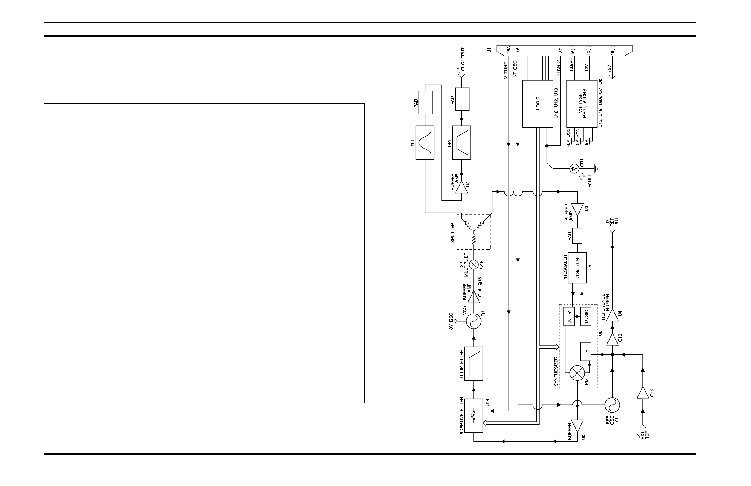
The divided reference signal and the divided multiplier
signal are compared in the PLL phase detector. When the
reference and multiplier signals are identical the PLL phase
detector generates a constant DC output voltage. This voltage
is buffered by U8 and filtered by the loop filter circuit. It is then
applied to Q1 setting the VCO on frequency.
If the compared frequencies (phases) differ, an error voltage
is generated which adjusts the VCO frequency. During this
out-of-lock condition, the PLL also sends a Lock Detect (LD)
signal to the controller and lights the FAULT LED on the front
panel of the module.
Copyright© June 1992 Ericsson GE Mobile Communications Inc.
Figure 1 - Receiver Synthesizer Block Diagram
Table 1 - General Specifications
ITEM SPECIFICATION
FREQUENCY TUNING
Mechanical
Electrical
Full Specifications
Degraded Specifications
Channel Spacing
INJECTION FREQ FREQ. BAND
424.4 MHz-451.4 MHz (G3) 450-470 MHz, 403-425 MHz
446.4 MHz-472.6 MHz (G7) 425-450 MHz, 470-495 MHz
401.4 MHz-421.4 MHz (G8) 380-400 MHz
470.6 MHz-490.6 MHz (G10) 492-512 MHz
391.4 MHz-421.4 MHz (G12) 370-390 MHz
2 MHz
3 MHz
6.25 kHz
FREQUENCY STABILITY
LO POWER OUTPUT
LO NOMINAL IMPEDANCE
PHASE NOISE
@ 25 kHz Offset
HUM AND NOISE
Companion Receiver
±1.5 ppm
2.0 dBm ±2 dBm
50 ohms
>-137 dBc/Hz
-55 dB
HARMONICS @ LO PORT
SWITCHING SPEED
CURRENT DRAIN
+13.8V
+12V
<-30 dBc
<50 ms
<200 mA
<50 mA
REFERENCE OSCILLATOR
Frequency Output
Power Output
Impedance
12.8 MHz ±1.5 dBm
1 dBm ±2 dBm
50 ohms
EXT. REFERENCE OSCILLATOR
Frequency
Power
Impedance
5.00 MHz to 17.925 MHz (must be integer
divisible by the channel spacing)
+10 dBm ±3 dBm into 50 ohms
50 ohms
This manual is published by Ericsson Inc., without any warranty. Improvements and changes to this manual necessitated by typographical errors,
inaccuracies of current information, or improvements to programs and/or equipment, may be made by Ericsson Inc., at any time and without
notice. Such changes will be incorporated into new editions of this manual. No part of this manual may be reproduced or transmitted in any form
or by any means, electronic or mechanical, including photocopying and recording, for any purpose, without the express written permission of
Ericsson Inc.
LBI-38672J
1

CIRCUIT ANALYSIS
The Receiver Synthesizer Module consists of the follow-
ing circuits:
•Voltage Controlled Oscillator
•Multiplier (Frequency Doubler)
•Buffer Amplifiers
•Reference Oscillator and Buffer
•Prescaler and Synthesizer
•Loop Filter
•Digital Control
•Voltage Regulators
VOLTAGE CONTROLLED OSCILLATOR
The free running Voltage Controlled Oscillator (VCO) is
composed of a grounded-gate JFET (Q1) and associated
circuitry. Inductor L10 and associated capacitors form the
resonant tank circuit. The circuit’s use of high-Q components
minimizes phase noise.
Frequency tuning of the VCO is done by changing the
DC output voltage level from the loop filter U14. The Loop
Filter Out signal from U14 is routed through L4 and R3 and
applied to the two varicap diodes D4 and D5. The voltage
level applied determines the diodes’ capacitance and sets the
resonant frequency of the oscillator. If the VCO drifts or the
frequency is changed, the DC voltage level changes causing
the VCO’s resonant frequency to change. The output of the
oscillator is then applied to a buffer amplifier. Course adjust-
ment of frequency is done by adjusting trimmer capacitor
C52 while applying a calibration voltage to the V_TUNE line
connected to U14.4 pin 11.
FREQUENCY DOUBLER
Transistors Q14 and Q15 form a buffer stage to drive
transistor multiplier Q16. They isolate VCO Q1 from loading
effects which would degrade oscillator loaded Q and hence
noise performance. Transistor multiplier Q16 is tuned to pass
the second harmonic of the VCO output and hence serves as
a frequency doubler. Tank elements L1, C97-C99 and L12
form a resonant circuit and matching network to drive the
resistive splitter (R13, R17, R18, R96, R97, R99, R100).
RF AMPLIFIERS
The RF chain begins with a resistive splitter (R13, R17,
R18, R96, R97, R99 and R100). The output of the splitter at
R99 is attenuated by 7.5 dB and provides impedance match-
ing to Helical Filter FL1 which is tuned to pass the LO
Frequency while rejecting harmonics by about 40 dB. The
output of FL1 is fed thru resistive pad R12, R14 and R15 to
MMIC Amp U2 which operates in compression. Output
Amp U2 is followed by a bandpass filter (L13-L15, C86, C87
and C101) and resistive attenuator (R30, R101 and R102).
The final output at the front panel BNC connector J2 is
nominally 1.5 dBm and drives the Receiver Front End LO
input.
The other output at the resistive splitter at R100 is attenu-
ated by 20 dB and drives buffer amp U3 into compression.
U3 drives the synthesizer prescaler, providing a feedback
signal for the synthesizer phase locked loop.
REFERENCE OSCILLATOR AND BUFFER
The reference oscillator section provides a reference sig-
nal to the PLL section. The circuit design allows using either
an external or internal oscillator.
When using an external oscillator, the internal oscillator
is disabled by placing a logic low on the INT OSC line from
the T/R Shelf Interface Board. A high precision external
oscillator may then be connected to the module through the
external reference oscillator connector J4, EXT REF IN. J4
has a 50 ohm input impedance and is coupled to the base of
Q12. Buffer Q12 conditions the signal and applies it to the
synthesizer U6 via coupling capacitor C10.
The internal reference oscillator, Y1, provides a 12.8
MHz signal with a stability of ±1.0 ppm. It is enabled by
applying a logic high signal on the INT OSC line. This signal
turns on Q2, allowing it to conduct and apply +5 volts to pin
1 of the oscillator Y1. The 12.8 MHz output signal (Y1 pin
2) is then sent to the synthesizer via coupling capacitor C9.
The reference oscillator signal, either external or internal,
is also routed to Q13 via coupling capacitor C54. The output
taken from the emitter of Q13 is applied through C11 to the
input of Buffer Amplifier U4. The buffered signal is coupled
through C12 to a low pass filter network (C32,C33,C34, and
L7) and a resistive pad (R27, R28, and R31) for isolation.
The output from the resistive pad is then connected to J3,
REF OUT, making the reference oscillator signal available
for external use.
PRESCALER AND SYNTHESIZER IC
The integrated circuit U6 is the heart of the synthesizer. It
contains the necessary frequency dividers and control circuitry
to synthesize output frequencies by the technique of dual
modulus prescaling. U6 also contains an analog sample and
hold phase detector and a lock detector circuit.
Within U6 are three programmable dividers which are
serially loaded using the CLOCK, DATA, and ENABLE inputs
(pins 11, 12, and 13 respectively). A serial data stream (DATA)
on pin 12 is shifted into the internal shift registers by low to
high transitions on the clock input (CLOCK) at pin 11. A logic
high (ENABLE) on pin 13 then transfers the program informa-
tion from the shift registers to the divider latches. The serial
data determines the VCO frequency by setting the internal R,
A, and N dividers.
The 12.8 MHz reference oscillator signal OSCIN is inter-
nally routed to the "R" divider. The "R" divider divides down
the 12.8 MHz reference signal to a lower frequency, Fr, as
directed by the input data and applies the signal to the internal
analog phase and lock detectors.
The "A" and "N" dividers process the loop feedback signal
from the multiplier (by way of the dual modulus prescaler U5).
The output of the "N" divider, Fv, is a divided down version of
the multiplier output frequency. This signal is also applied to
the internal phase detector. The ramp and hold constants are
determined by C26, R37, C31, and R36.
The analog phase detector output voltage (PD OUT) is
proportional to the phase difference between Fv and Fr. This
output serves as the loop error signal. When operating on the
correct frequency, the inputs to the phase detector are identical
and the output voltage of the analog phase detector is constant.
If the compared frequencies (phases) differ, the analog phase
detector increases or decreases the DC output voltage (PD
OUT). This error signal voltage tunes the VCO to whatever
frequency is required to keep Fv and Fr locked (in phase).
The lock detector furnishes the Fault circuit in U13 with
the lock detect (LD) signal. When Fv and Fr are in phase, the
lock detector output sends a logic high on the LD line to the
fault circuit U13. If the VCO is not locked onto the correct
frequency, the resulting out-of-phase condition causes the out-
put from the lock detector to be a logic low.
LOOP FILTER
The error signal, ANOUT, is applied to the loop filter at
U8.2 pin 5 and U8.1 pin 3. U8.2 acts as a buffer amplifier with
gain. The output signal from the amplifier is applied to a loop
filter consisting of R42, R43, R44, C35 and C36 via the
bilateral switch U14. The filter removes noise and sampling
frequencies from the error voltage. The switch, U14, selects the
proper filter configuration for operation in the narrow band,
wide band or tuning mode. The control signals (OPEN_LOOP,
ENABLE_NOT, and TUNE_CTRL) for U14 are derived from
the digital control circuits U10, U12, and U13. U8.1 provides
a buffered output for testing at the DIN connector on the rear
of the module.
DIGITAL CONTROL
Logic control circuits (other than those inside the synthe-
sizer IC - U6) consist of the following:
•Digital Control Circuit (U10, U12, & U13)
•Level Shifters
•Fault Circuit
The Digital Control Circuits U10, U12, & U13 serve as an
interface between the controller and the synthesizer IC.
As an address decoder, U10 enables the input gates when
the A0, A1, and A2 input lines (pins 4, 3, and 2) receive the
correct address code from the controller. For the Receiver
synthesizer the enable address is 010 on A0, A1, and A2
respectively. After receiving the proper logic code, the input
gate U12 is enabled. This allows the ENABLE, CLOCK, and
serial DATA information to pass on to the synthesizer via the
level shifters.
The Level Shifters Q3, Q4, and Q5 convert the five volt
logic level to the eight volt logic level required by the synthe-
sizer.
The Fault circuit, U13, monitors the lock detect signal from
the PLL synthesizer. Under normal (locked) condition, the PLL
sends a logic high signal to U13. U13 processes the signal and
provides a logic high output which saturates Q6. Saturating Q6
turns off the FAULT LED (CR1). U13 also sends a logic high
signal, FLAG 2, (U13.3 pin 8) to the controller indicating the
VCO’s frequency is correct.
LBI-38672J
2
When the VCO is not on the correct frequency, the synthe-
sizer sends a logic low signal to U13. This causes U13 to cutoff
Q6 which turns on the FAULT LED (CR1). U13 also sends a
logic low signal to the controller, on the FLAG 2 line, indicat-
ing the VCO’s frequency is incorrect.
VOLTAGE REGULATORS
Voltage regulators U15 and U16 reduce the +13.8 VF line
to +5 Vdc and +8 Vdc respectively. The output from U15
(+5V_SYN) is used by both the synthesizer and logic circuitry
while the 8 Vdc output from U16 is used for the op-amps, level
shifters, and the discrete +8V OSC regulator circuit.
The discrete +8V OSC regulator circuit is a linear regulator
consisting of U9A, Q7, Q8, and associated circuitry. The error
amplifier U9A controls Q7 and pass element Q8. The +8V OSC
is used as the power source for the VCO circuit, where addi-
tional filtering is provided to keep noise to a minimum
MAINTENANCE
RECOMMENDED TEST EQUIPMENT
The following test equipment is required to test the Synthe-
sizer Module:
1. Modulation Analyzer; HP 8901A, or equivalent
2. Power Supply; 12.0 Vdc @ 500 mA
3. Frequency Counter; 10 MHz - 250 MHz
4. Power Meter; -20 dBm to +10 dBm
5. Spectrum Analyzer, 0 - 1 GHz
TEST AND ALIGNMENT
INITIALIZATION
Apply +12 Vdc to the test fixture.
Current Consumption
Measure the current through pins 15A, 15B, 15C, 16A,
16B, AND 16C.
Verify the current is less than 250 mA. Total current
is the +13.8 VF current and +12 Vdc current com-
bined.
Reference Oscillator
Adjust Y1 for an output frequency of 12.8 MHz ±2 Hz.
Measure the output power of the reference oscillator output
(J3).
Verify the output power is 1 dBm ±2 dBm.
Oscillator Alignment
Ground the ENABLE TEST line (pin 22A). Apply +4
Vdc to the V_TUNE line (pin 26A). Measure the frequency
of the free running multiplied oscillator at the LO OUT port
(J2).
Adjust the trimmer capacitor C52 for 445 MHz
(G3), 470 MHz (G7), 420 MHz (G8), 490 MHz
(G10), 420 MHz (G12) or desired injection fre-
quency ±100 kHz.
Synthesizer Loading
Unground the ENABLE TEST line (pin 22A). Load the
synthesizer IC for 445 MHz (G3) or 470 MHz (G7) or 420
MHz (G8), 490 MHz (G10), 420 MHz (G12) or desired
injection frequency.
Verify the lock indicator (CR1) is off or the FLAG
2 line is high.
Hum and Noise
Initialize the HP 8901A for 300 Hz - 3 kHz, 750 µsec
de-emphasis, average FM deviation, and 0.44 dB reference
for the deviation.
Verify the hum and noise (J2) is less than -55 dB.
Output Power and Harmonic Content
Adjust both slugs on FL1 for maximum output level
measured at J2.
Verify the output power (J2) at the fundamental fre-
quency is:
2 dBm ±2 dB
Verify the harmonic content is less than -30 dBc.
The following service information applies when aligning,
testing, or troubleshooting the RX Synthesizer:
•Logic Levels:
Logic 1 = high = 4.5 to 5.5 Vdc
Logic 0 = Low = 0 to 0.5 Vdc
•Receiver Synthesizer Address = A0 A1 A2 = 010
•Synthesizer data input stream is as follows:
14-bit "R" divider most significant bit (MSB) = R13
through "R" divider least significant (LSB) = R0
10-bit "N" divider MSB = N9 through "N" divider
LSB = N0
7-bit "A" divider MSB = A6 through "A" divider
LSB = A0
Single high Control bit (last bit)
Latched When Control Bit = 1
DATA ENTRY FORMAT
Latched When
Control Bit = 1
Last
Bit A0
LSB - - - A6
MSB N0
MSB - - N0
MSB R0
LSB - - - R13
MSB
Control Bit
•Synthesizer lock is indicted by the extinguishing of the
front panel LED indicator and a logic high on the fault
FLAG 2 line (J1 pin 12C).
•Always verify synthesizer lock after each new data
loading.
SERVICE NOTES
Data in→Shift
→Register
Out
LBI-38672J
3
TROUBLESHOOTING CHART
SYMPTOM AREAS TO CHECK INDICATIONS
I. Loop Fails To Lock 1. Check for:
+8 Vdc at U16-3,
+5 Vdc at U15-3
+8 Vdc at Q8-C.
2. Check for 12.8 MHz
reference at U6-2 and U6-3.
Typical Levels:
500 mVpp @U6-2
2.5 Vpp @U6-3.
3. Check for LO output @J2.
FLO ±5 MHz, 0 dBm nominal
4. Check Prescaler output @U5-4.
Typically: 2-4 MHz square wave
@1.25 Vpp.
5. Check for CLOCK, DATA,
and ENABLE signals at U6
pins 11, 12 and 13 respectively.
(0, 8V logic levels)
6. Check Ramp Signal @U6-15.
It should be 6.25 kHz nominal.
Bad Regulation circuitry.
Troubleshooting using
standard procedures.
Reference Osc. Module defective or supply
not present or low. Proceed to reference
oscillator section II.
LO tuning incorrect, or buffer amplifier bad.
Proceed to LO tuning and power section III.
If LO power is good, check for 3.2 Vdc
@U2-3. Replace U2, then U5 if necessary.
Bad digital control circuitry.
Troubleshoot using standard procedures.
Ensure all programming signals are present
at J1. (CLOCK, DATA, ENABLE, A0, A1
and A2).
If reference oscillator and programming
signals are present for proper programming
information. Last resort - replace
Synthesizer IC U6.
II. Reference OSC. not present or
low power. 1. Check for 4.3 Vdc supply at
junction of R5 and C41.
2. Check 12.8 MHz signal @Q13-E.
Should be approx. 350 mVpp.
Bad supply switch Q2 or wrong
Control Signal Internal Osc.
Troubleshooting using standard procedures.
Replace Y1 as last resort.
Bad buffer amplifier Q13.
Troubleshoot using standard procedures.
III. LO power low or
tuned out of band. 1. Check tuning with 6 Vdc applied
using test procedure. FLO ±5 MHz.
2. Check DC bias at Buffer
Amplifiers U1, U2, & U3 pin 3
Typ. 3.2 Vdc.
LO tuning incorrect. Retune following
test procedure.
Bad Buffer Amplifier. Replace bad part.
IV. LO signal not present.
(i.e. Q1 does not oscillate) 1. Check DC bias at Q1 drain.
(Typ. +8Vdc).
2. Check DC bias at Q1 source.
(Typ. +0.9 Vdc).
Replace Q1.
LBI-38672J
4
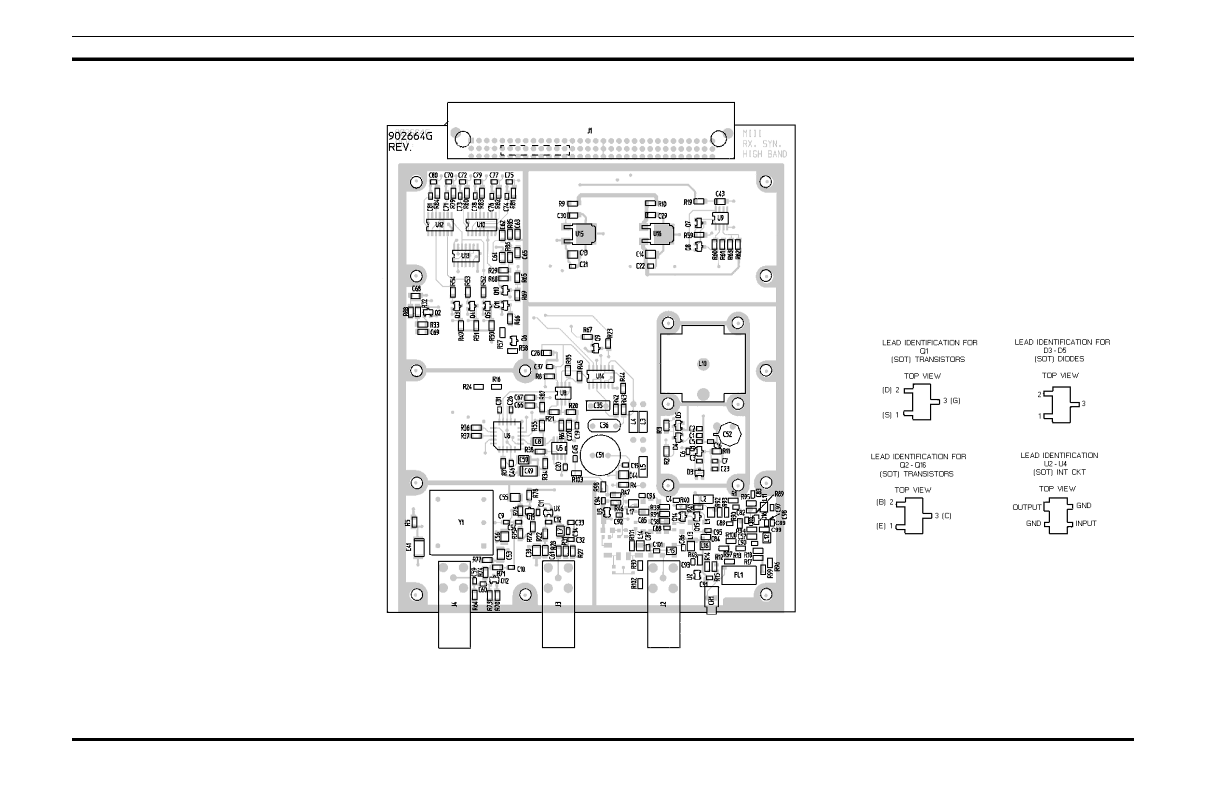
OUTLINE DIAGRAM
UHF RECEIVER SYNTHESIZER BOARD
19D902664G3 ,G7, G8, G10, G12
COMPONENT SIDE
(19D902664, Sh. 2, Rev. 4)
(19D902665, Layer 1, Rev. 1)
LBI-38672J
5
PARTS LIST
UHF RECEIVER SYNTHESIZER MODULE
19D902781G3, G7, G8, G10, G12
ISSUE 8
SYMBOL PART NO. DESCRIPTION
- - - - - - - - - MISCELLANEOUS - - - - - - - - -
3 19D902509P4 COVER.
4 19D902555P1 Handle.
6 19A702381P506 Screw, thread forming: TORX, No. M3.5-.6 x 6.
7 19A702381P513 Screw, thread forming: TORX, No. M3.5 - 0.6 X
13.
10 19D902824P1 Casting.
11 19A702381P508 Screw, thd. form: No. 3.5-0.6 x 8.
38 19B802690P1 Grommet.
UHF RECEIVER SYNTHESIZER BOARD
19D902664G3, G7, G8, G10, G12
- - - - - - - - - - CAPACITORS - - - - - - - - -
C1 19A702236P15 Ceramic: 3.9 pF + or -0.25 pF, 50 VDCW, temp coef
0 + or -30 PPM/°C. (Used in G7, G3, G10).
C1 19A702236P17 Ceramic: 4.7 pF + or -0.5 pF, 50 VDCW, temp coef
0 + or -60 PPM/°C. (Used in G8, G12).
C2 19A702236P6 Ceramic: 1 pF + or -0.25 pF, 50 VDCW, temp coef 0
+ or -30 PPM/°C. (Used in G3).
C2 19A702236P15 Ceramic: 3.9 pF + or -0.25 pF, temp coef 0 + or
-30 PPM/°C. (Used in G8).
C2 19A702236P19 Ceramic: 5.6 pF + or -0.5 pF, 50 VDCW, temp coef 0
+ or -60 PPM/°C. (Used in G12).
C3 19A702236P38 Ceramic: 33 pF + or -5%, 50 VDCW, temp coef 0 +
or -30 PPM/°C. (Used in G3).
*C3 19A702236P36 Ceramic: 27 pF + or -5%, 50 VDCW, temp coef 0 +
or -30 PPM/°C. (Used in G7 , G8and G12).
C3 19A702236P34 Ceramic: 22 pF + or -5%, 50 VDCW, temp coef 0 +
or -30 PPM. (Used in G10).
C4 19A702236P9 Ceramic: 1.8 pF + or -0.25 pF, 50 VDCW, temp coef
0 + or -30 PPM.
C5 19A702236P30 Ceramic: 15 pF + or -5%, 50 VDCW, temp coef 0 +
or -30 PPM/°C. (Used in G3).
*C5 19A702236P28 Ceramic: 12 pF + or - 5%, 50 VDCW, temp coef 0
+ or -30 PPM. (Used in G7, G8, G10, G12).
C6 19A702236P36 Ceramic: 27 pF + or -5%, 50 VDCW, temp coef 0 +
or -30 PPM/°C. (Used in G3).
*C6 19A702236P34 Ceramic: 22 pF + or -5%, 50 VDCW, temp coef 0 +
or -30 PPM. (Used in G7 and G8, G12).
C6 19A702236P32 Ceramic: 18 pF + or -5%, 50 VDCW, temp coef 0 +
or -30 PPM. (Used in G10).
C7 19A702052P14 Ceramic: 0.01 uF + or - 10%, 50 VDCW.
C8 19A702052P26 Ceramic: 0.1uF + or - 10%, 50 VDCW.
C9 19A702052P14 Ceramic: 0.01 uF + or - 10%, 50 VDCW.
C10 19A702052P14 Ceramic: 0.01 uF + or - 10%, 50 VDCW.
C11 19A702052P14 Ceramic: 0.01 uF + or - 10%, 50 VDCW.
C12 19A702052P14 Ceramic: 0.01 uF + or - 10%, 50 VDCW.
C13 19A702052P26 Ceramic: 0.1uF + or - 10%, 50 VDCW
and
C14
C15 19A702052P5 Ceramic: 1000 pF + or -10%, 50 VDCW.
*C16 19A702236P25 Ceramic: 10 pF + or -.5 pF, 50 VDCW, temp coef
0 + -30 PPM/°C. (Used in G3, G7 & G10).
C16 19A702236P28 Ceramic: 12 pF + or -.5 pF, 50 VDCW, temp coef
0 + -30 PPM/°C. (Used in G8).
C16 19A702236P31 Ceramic: 16 pF + or - 5%, 50 VDCW, temp coef
0 + -30 PPM/°C. (Used in G12).
C19 19A702052P3 Ceramic: 470 pF + or - 10%, 50 VDCW.
C20 19A702052P3 Ceramic: 470 pF + or - 10%, 50 VDCW.
* COMPONENTS, ADDED, DELETED OR CHANGED BY PRODUCTION CHANGES
SYMBOL PART NO. DESCRIPTION
C21 19A702052P3 Ceramic: 470 pF + or - 10%, 50 VDCW.
C22 19A702052P3 Ceramic: 470 pF + or - 10%, 50 VDCW.
C23 19A702052P5 Ceramic: 1000 pF + or -10%, 50 VDCW.
C26 19A702052P8 Ceramic: 3300 pF + or - 10%, 50 VDCW.
C27 19A705205P2 Tantalum: 1 uF, 16 VDCW; sim to Sprague 293D.
C28 19A705205P2 Tantalum: 1 uF, 16 VDCW; sim to Sprague 293D.
C29 19A705205P2 Tantalum: 1 uF, 16 VDCW; sim to Sprague 293D.
C30 19A705205P2 Tantalum: 1 uF, 16 VDCW; sim to Sprague 293D.
C31 19A702052P1 Ceramic: 220 pF + or - 10%, 50 VDCW.
C32 19A702052P1 Ceramic: 220 pF + or - 10%, 50 VDCW.
C33 19A702052P1 Ceramic: 220 pF + or - 10%, 50 VDCW.
C34 19A702236P43 Ceramic: 51 pF + or - 5%, 50 VDCW, temp coef
0 + - 30 PPM/°C.
C35 19A703684P1 Metallized Polyester: 0.47 uF + or -10%, 63 v.
C36 19A703902P3 Metal: 0.047 uF + or -10%, 50 VDCW.
C37 19A702052P14 Ceramic: 0.01 uF + or - 10%, 50 VDCW.
C38 19A702052P26 Ceramic: 0.1uF + or - 10%, 50 VDCW
C43 19A705205P2 Tantalum: 1 uF, 16 VDCW; sim to Sprague 293D.
C44 19A702052P26 Ceramic: 0.1uF + or - 10%, 50 VDCW.
C45 19A702052P3 Ceramic: 470 pF + or - 10%, 50 VDCW.
C46 19A702052P3 Ceramic: 470 pF + or - 10%, 50 VDCW.
C49 19A705205P6 Tantalum: 10 uF, 16 VDCW; sim to Sprague 293D.
C50 19A702052P26 Ceramic: 0.1uF + or - 10%, 50 VDCW.
C51 19A701225P3 Electrolytic: 220 uF, -10+50%, 25 VDCW.
C52 19A134227P5 Variable: 1.5 to 14 pF, 100 VDCW. (Used in G40,
G3 and G8).
C53 19A702052P26 Ceramic: 0.1uF + or - 10%, 50 VDCW.
C54 19A702052P14 Ceramic: 0.01 uF + or - 10%, 50 VDCW.
C55 19A702052P26 Ceramic: 0.1uF + or - 10%, 50 VDCW.
C56 19A702052P26 Ceramic: 0.1uF + or - 10%, 50 VDCW
C57 19A702061P99 Ceramic: 1000 pF + or -5%, 50 VDCW, temp coef 0
+ or -30 PPM/°C.
C58 19A702061P99 Ceramic: 1000 pF + or -5%, 50 VDCW, temp coef 0
+ or -30 PPM/°C.
C59 19A702052P14 Ceramic: 0.01 uF + or - 10%, 50 VDCW.
C60 19A702052P14 Ceramic: 0.01 uF + or - 10%, 50 VDCW.
C61 19A702061P99 Ceramic: 1000 pF + or -5%, 50 VDCW, temp coef 0
and + or -30 PPM/°C.
C62
C63 19A702061P99 Ceramic: 1000 pF + or -5%, 50 VDCW, temp coef 0
+ or -30 PPM/°C.
C64 19A702061P99 Ceramic: 1000 pF + or -5%, 50 VDCW, temp coef 0
+ or -30 PPM/°C.
C65 19A702061P99 Ceramic: 1000 pF + or -5%, 50 VDCW, temp coef 0
+ or -30 PPM/°C.
C66 19A702061P99 Ceramic: 1000 pF + or -5%, 50 VDCW, temp coef 0
+ or -30 PPM/°C.
C67 19A702061P99 Ceramic: 1000 pF + or -5%, 50 VDCW, temp coef 0
+ or -30 PPM/°C.
C68 19A702061P99 Ceramic: 1000 pF + or -5%, 50 VDCW, temp coef 0
+ or -30 PPM/°C.
C69 19A702061P99 Ceramic: 1000 pF + or -5%, 50 VDCW, temp coef 0
+ or -30 PPM/°C.
C70 19A702061P61 Ceramic: 100 pF + or - 5%, 50 VDCW, temp coef 0
+ or - 30 PPM.
C71 19A702061P61 Ceramic: 100 pF + or - 5%, 50 VDCW, temp coef 0
+ or - 30 PPM.
C72 19A702061P61 Ceramic: 100 pF + or - 5%, 50 VDCW, temp coef 0
+ or - 30 PPM.
SYMBOL PART NO. DESCRIPTION
C73 19A702061P61 Ceramic: 100 pF + or - 5%, 50 VDCW, temp coef 0
+ or - 30 PPM.
C74 19A702061P61 Ceramic: 100 pF + or - 5%, 50 VDCW, temp coef 0
+ or - 30 PPM.
C75 19A702061P61 Ceramic: 100 pF + or - 5%, 50 VDCW, temp coef 0
+ or - 30 PPM.
C76 19A702061P61 Ceramic: 100 pF + or - 5%, 50 VDCW, temp coef 0
+ or - 30 PPM.
C77 19A702061P61 Ceramic: 100 pF + or - 5%, 50 VDCW, temp coef 0
+ or - 30 PPM.
C78 19A702061P61 Ceramic: 100 pF + or - 5%, 50 VDCW, temp coef 0
+ or - 30 PPM.
C79 19A702061P61 Ceramic: 100 pF + or - 5%, 50 VDCW, temp coef 0
+ or - 30 PPM.
C80 19A702061P61 Ceramic: 100 pF + or - 5%, 50 VDCW, temp coef 0
+ or - 30 PPM.
C81 19A702061P61 Ceramic: 100 pF + or - 5%, 50 VDCW, temp coef 0
+ or - 30 PPM. (Used in G40, G3, G7 and G8).
C82 19A702052P14 Ceramic: 0.01 uF + or - 10%, 50 VDCW. (Used in
and G80, G5, G40,
C83
C84 19A702061P99 Ceramic: 1000 pF + or -5%, 50 VDCW, temp coef 0
+ or -30 PPM/°C.
C85 19A702061P99 Ceramic: 1000 pF + or -5%, 50 VDCW, temp coef 0
+ or -30 PPM/°C.
C86 19A702236P28 Ceramic: 12 pF + or - 5%, 50 VDCW, temp coef 0
and + or -30 PPM. (Used in G80, G5, G40, G3, G7 and
C87 G8).
C88 19A702052P14 Ceramic: 0.01 uF + or - 10%, 50 VDCW.
C89 19A702061P61 Ceramic: 100 pF + or - 5%, 50 VDCW, temp coef 0
+ or - 30 PPM.
C90 19A702052P14 Ceramic: 0.01 uF + or - 10%, 50 VDCW. (Used in
G40, G3, G7
C91 19A702061P61 Ceramic: 100 pF + or - 5%, 50 VDCW, temp coef 0
+ or - 30 PPM. (Used in G80, G5, G40, G3, G7 and
G8).
C92 19A702061P61 Ceramic: 100 pF + or - 5%, 50 VDCW, temp coef 0
thru + or - 30 PPM. (Used in G40, G3, G7 and G8).
C96
C97 19A702236P1 Ceramic: 0.5 pF + or -.l pF, 50 VDCW, temp coef
-30 PPM. (Used in G3, and G7).
C97 19A702236P11 Ceramic: 2.7 pF + or -.25 (Used in G8, G12).
C98 19A702236P30 Ceramic: 15 pF + or -5%, 50 VDCW, temp coef 0 +
and or -30 PPM/°C. (Used in G3, and G7).
C99
C98 19A702236P31 Ceramic: 16 pF + or -5%, 50 VDCW, temp coef 0 +
and or -30 PPM/°C. (Used in G8, G12).
C99
C98
and
C99
19A702236P28 Ceramic: 12 pF + or -5%, 50 VDCW, temp coef 0 +
or -30 PPM/°C. (Used in G10).
C100 19A702236P25 Ceramic: 10 pF + or -.5 pF, 50 VDCW, temp coef
-30 PPM/°C.
C101 19A702236P10 Ceramic: 2.2 pF + or -2.5 pF, 50 VDCW, temp
or -30 PPM/°C.
- - - - - - - - - - - DIODES - - - - - - - - - -
CR1 19A703595P10 Optoelectic: Red LED; sim to HP HLMP-1301-010.
- - - - - - - - - - - FILTERS - - - - - - - - - -
FL1 344A3802P4 FILTER ,HEL RF (Used in G8).
FL1 344A3802P2 FILTER ,HEL RF (Used in G3).
FL1 344A3802P3 FILTER, RF: 475 MHz SIM TO TOKO
SHW-44545A-475 (Used in G7, G10)
FL1 344A3802P5 FILTER ,HEL RF: sim to TOKO
SHW-39545A-415 (Used in G12).
- - - - - - - - - - - JACKS - - - - - - - - - - -
J1 19B801587P7 Connector, DIN: 96 male contacts, right angle
to AMP 650887-1.
J2 19A115938P24 Connector, receptacle.
thru
J4
SYMBOL PART NO. DESCRIPTION
- - - - - - - - - - INDUCTORS - - - - - - - - - -
*L2 19A705470P25 Coil, fixed: .1uH; sim to Toko 380LB-1R0M.
L3 19A700024P13 Coil, RF: 1.0 uH + or -10%.
and
L4
L5 19A700024P15 Coil, RF: 1.5 uH + or - 10%.
L10 19C851001P4 Coil, RF: sim to Paul Smith SK901-1.
- - - - - - - - - - - CRYSTALS - - - - - - - - -
Y1 19B801351P14 Module: Crystal Oscillator, 12.8 MHz + or -1.0
PPM.
- - - - - - - - - - - DIODES - - - - - - - - - -
D3 19A705377P1 Silicon, Hot Carrier: sim to MMB0201.
D4 19A149674P1 DIODE ,SILICON.
and
D5
- - - - - - - - - - INDUCTORS - - - - - - - - - -
L1 19A705470P2 Coil, Fixed: 12 nH; sim to Toko 380NB-12nM.
L7 19A705470P24 Coil, Fixed: 0.82 uH; sim to Toko 380NB-R82M.
L11 19A705470P2 Coil, Fixed: 12 nH; sim to Toko 380NB-12nM.
and
L12
L13 19A705470P1 Coil, Fixed: 10 nH; sim to Toko 380NB-10nM.
and
L14
L15 19A705470P10 Coil, fixed: 56 nH; sim to Toko 380NB-56nM.
L16 19A705470P15 Coil, fixed: .15uH; sim to Toko 380NB-R15M.
and
L17
- - - - - - - - - - TRANSISTORS - - - - - - - - -
Q1 19A702524P2 N-Type, field effect; sim to MMBFU310.
Q2 19A700076P2 Silicon, NPN: sim to MMBT3904, low profile.
Q3 19A700076P2 Silicon, NPN: sim to MMBT3904, low profile.
thru
Q5
Q6 19A700076P2 Silicon, NPN: sim to MMBT3904, low profile.
Q7 19A700076P2 Silicon, NPN: sim to MMBT3904, low profile.
Q8 19A700059P2 Silicon, PNP: sim to MMBT3906, low profile.
Q9 19A700076P2 Silicon, NPN: sim to MMBT3904, low profile.
thru
Q11
Q12 19A700076P2 Silicon, NPN: sim to MMBT3904, low profile.
and
Q13
Q14 19A704708P2 Silicon, NPN: sim to NEC 2SC3356.
thru
Q16
- - - - - - - - - - RESISTORS - - - - - - - - - -
R1 19B800607P680 Metal film: 68 ohms + or -5%, 1/8 w.
R2 19B800607P100 Metal film: 10 ohms + or -5%, 1/8 w. (Used in
G40, G3, G7
R3 19B800607P100 Metal film: 10 ohms + or -5%, 1/8 w.
R4 19B800607P100 Metal film: 10 ohms + or -5%, 1/8 w.
R5 19B800607P100 Metal film: 10 ohms + or -5%, 1/8 w.
thru
R9
R10 19B800607P1 Metal film: 0 ohms.
R11 19B800607P183 Metal film: 18K ohms + or -5%, 1/8 w.
R12 19B800607P271 Metal film: 270 ohms + or -5%, 1/8 w.
R13 19B800607P510 Metal film: 51 ohms + or -5%, 1/8 w.
R14 19B800607P271 Metal film: 270 ohms + or -5%, 1/8 w.
R15 19B800607P180 Metal film: 18 ohms + or -5%, 1/8 w.
R16 19B800607P392 Metal film: 3.9K ohms + or -5%, 1/8 w.
LBI-38672J
6
PARTS LIST & PRODUCTION CHANGES
PRODUCTION CHANGES
Changes in the equipment to improve performance or to simplify circuits are
identified by a "Revision Letter" which is stamped after the model number of
the unit. The revision stamped on the unit includes all previous revisions. Refer
to the Parts List for the descriptions of parts affected by these revisions.
REV. A - UHF RECEIVER SYNTHESIZER BOARD 19D902664G3
The UHF Receiver Synthesizer module was modified to
meet ETSI requirements.
Items 3 and 7 were changed and item 23 was added.
Item 3 was: 19D902509P3.
Item 7 was: 19A702381P513.
C16 was 6.8 pF (19A702236P21).
C2 was deleted (19A702236P10).
REV. A - UHF RECEIVER SYNTHESIZER BOARD 19D902664G7
REV. B - UHF RECEIVER SYNTHESIZER BOARD 19D902664G3
To improve operation.
C3 was 22 pF (19A702236P34).
C5 was 10 pF (19A702236P25).
C6 was 18 pF (19A702236P32).
C16 was 8.2 pF (19A702236P23).
R4 was 47 ohms (19B800607P470).
REV. B - UHF RECEIVER SYNTHESIZER BOARD 19D902664G7
REV. C - UHF RECEIVER SYNTHESIZER BOARD 19D902664G3
To support 12.5kHz operation, changed Y1.
Was 1.5PPM crystal (19B801351P12).
REV. C - UHF RECEIVER SYNTHESIZER BOARD 19D902664G7
To reduce spurious radiation to meet ETSI specs.
L12 and R18 interchanged. L2 was 1uH (19A700024P13).
REV. D - UHF RECEIVER SYNTHESIZER BOARD 19D902664G3 & G7
To prevent regulator from drop out at low voltages.
R10 was 10 ohms (19B800607P100).
REV. E - UHF RECEIVER SYNTHESIZER BOARD 19D902664G3
To correct timing range added C2 (and changed C16).
C16 was 8.2 pF (19A702236P23).
SYMBOL PART NO. DESCRIPTION
R17 19B800607P120 Metal film: 12 ohms + or -5%, 1/8 w.
R18 19B800607P180 Metal film: 18 ohms + or -5%, 1/8 w.
R19 19B800607P100 Metal film: 10 ohms + or -5%, 1/8 w.
R20 19B800607P103 Metal film: 10K ohms + or -5%, 1/8 w.
R21 19B800607P472 Metal film: 4.7K ohms + or -5%, 1/8 w.
R22 19B800607P271 Metal film: 270 ohms + or -5%, 1/8 w.
R23 19B800607P103 Metal film: 10K ohms + or -5%, 1/8 w.
R24 19B800607P562 Metal film: 5.6K ohms + or -5%, 1/8 w.
R27 19B800607P181 Metal film: 180 ohms + or -5%, 1/8 w.
R28 19B800607P181 Metal film: 180 ohms + or -5%, 1/8 w.
R29 19B800607P103 Metal film: 10K ohms + or -5%, 1/8 w.
R30 19B800607P560 Metal film: 56 ohms + or -5%, 1/8 w.
(Used in G3, G7, G8, G12).
R30 19B800607P680 Metal film: 68 ohms + or -5%, 1/8 w. (Used in G10).
R31 19B800607P270 Metal film: 27 ohms + or -5%, 1/8 w.
R32 19B800607P472 Metal film: 4.7K ohms + or -5%, 1/8 w.
R33 19B800607P472 Metal film: 4.7K ohms + or -5%, 1/8 w.
R34 19B800607P103 Metal film: 10K ohms + or -5%, 1/8 w.
R35 19B800607P103 Metal film: 10K ohms + or -5%, 1/8 w.
R36 19B800607P393 Metal film: 39K ohms + or -5%, 1/8 w.
R37 19B800607P104 Metal film: 100K ohms + or -5%, 1/8 w.
R38 19B800607P682 Metal film: 6.8K ohms + or -5%, 1/8 w.
R39 19B800607P102 Metal film: 1K ohms + or -5%, 1/8 w.
R40 19B800607P102 Metal film: 1K ohms + or -5%, 1/8 w.
R41 19B800607P102 Metal film: 1K ohms + or -5%, 1/8 w.
R42 19B800607P823 Metal film: 82K ohms + or -5%, 1/8 w.
R43 19B800607P333 Metal film: 33K ohms + or -5%, 1/8 w.
R44 19B800607P274 Metal film: 270K ohms + or -5%, 1/8 w.
R45 19B800607P472 Metal film: 4.7K ohms + or -5%, 1/8 w.
R46 19B800607P181 Metal film: 180 ohms + or -5%, 1/8 w.
R47 19B800607P271 Metal film: 270 ohms + or -5%, 1/8 w.
R48 19B800607P181 Metal film: 180 ohms + or -5%, 1/8 w.
R49 19B800607P103 Metal film: 10K ohms + or -5%, 1/8 w.
R50 19B800607P103 Metal film: 10K ohms + or -5%, 1/8 w.
R51 19B800607P103 Metal film: 10K ohms + or -5%, 1/8 w.
R52 19B800607P473 Metal film: 47K ohms + or -5%, 1/8 w.
R53 19B800607P473 Metal film: 47K ohms + or -5%, 1/8 w.
R54 19B800607P473 Metal film: 47K ohms + or -5%, 1/8 w.
R55 19B800607P222 Metal film: 2.2K ohms + or -5%, 1/8 w.
R57 19B800607P473 Metal film: 47K ohms + or -5%, 1/8 w.
R58 19B800607P681 Metal film: 680 ohms + or -5%, 1/8 w.
R59 19B800607P222 Metal film: 2.2K ohms + or -5%, 1/8 w.
R60 19B800607P102 Metal film: 1K ohms + or -5%, 1/8 w.
R61 19B800607P102 Metal film: 1K ohms + or -5%, 1/8 w.
R62 19B800607P102 Metal film: 1K ohms + or -5%, 1/8 w.
R63 19B800607P102 Metal film: 1K ohms + or -5%, 1/8 w.
R64 19B800607P510 Metal film: 51 ohms + or -5%, 1/8 w.
R65 19B800607P103 Metal film: 10K ohms + or -5%, 1/8 w.
R66 19B800607P103 Metal film: 10K ohms + or -5%, 1/8 w.
R67 19B800607P473 Metal film: 47K ohms + or -5%, 1/8 w.
R68 19B800607P473 Metal film: 47K ohms + or -5%, 1/8 w.
R69 19B800607P333 Metal film: 33K ohms + or -5%, 1/8 w.
R70 19B800607P102 Metal film: 1K ohms + or -5%, 1/8 w.
SYMBOL PART NO. DESCRIPTION
R71 19B800607P102 Metal film: 1K ohms + or -5%, 1/8 w.
R72 19B800607P102 Metal film: 1K ohms + or -5%, 1/8 w.
R73 19B800607P103 Metal film: 10K ohms + or -5%, 1/8 w.
R74 19B800607P103 Metal film: 10K ohms + or -5%, 1/8 w.
R75 19B800607P103 Metal film: 10K ohms + or -5%, 1/8 w.
R76 19B800607P103 Metal film: 10K ohms + or -5%, 1/8 w.
R77 19B800607P101 Metal film: 100 ohms + or -5%, 1/8 w.
R78 19B800607P101 Metal film: 100 ohms + or -5%, 1/8 w.
R79 19B800607P102 Metal film: 1K ohms + or -5%, 1/8 w.
R80 19B800607P102 Metal film: 1K ohms + or -5%, 1/8 w.
R81 19B800607P102 Metal film: 1K ohms + or -5%, 1/8 w.
R82 19B800607P102 Metal film: 1K ohms + or -5%, 1/8 w.
R83 19B800607P102 Metal film: 1K ohms + or -5%, 1/8 w.
R84 19B800607P102 Metal film: 1K ohms + or -5%, 1/8 w.
R85 19B800607P102 Metal film: 1K ohms + or -5%, 1/8 w.
R86 19B800607P102 Metal film: 1K ohms + or -5%, 1/8 w.
R87 19B800607P102 Metal film: 1K ohms + or -5%, 1/8 w.
R88 19B800607P102 Metal film: 1K ohms + or -5%, 1/8 w.
R89 19B800607P103 Metal film: 10K ohms + or -5%, 1/8 w.
R90 19B800607P222 Metal film: 2.2K ohms + or -5%, 1/8 w.
R91 19B800607P101 Metal film: 100 ohms + or -5%, 1/8 w.
R92 19B800607P101 Metal film: 100 ohms + or -5%, 1/8 w.
thru
R94
R95 19B800607P101 Metal film: 100 ohms + or -5%, 1/8 w.
R96 19B800607P221 Metal film: 220 ohms + or -5%, 1/8 w.
R97 19B800607P220 Metal film: 22 ohms + or -5%, 1/8 w.
R98 19B800607P180 Metal film: 18 ohms + or -5%, 1/8 w.
R99 19B800607P120 Metal film: 12 ohms + or -5%, 1/8 w.
R100 19B800607P330 Metal film: 33 ohms + or -5%, 1/8 w.
R101
and
R102
19B800607P121 Metal film: 120 ohms + or -5%, 1/8 w.
(Used in G3, G7, G8, G12).
R101
and
R102
19B800607P101 Metal film: 100 ohms + or -5%, 1/8 w. (Used in G10).
R103 19B800607P390 Metal film: 39 ohms + or -5%, 1/8 w.
- - - - - - - - INTEGRATED CIRCUITS - - - - - - -
U2 19A705927P1 Silicon, bipolar: sim to Avantek MSA-0611.
U3 19A705927P1 Silicon, bipolar: sim to Avantek MSA-0611.
U4 19A705927P1 Silicon, bipolar: sim to Avantek MSA-0611.
U5 19A149944P201 Dual Modulus Prescaler: sim to Motorola
MC12022A.
U6 19B800902P5 Synthesizer, custom: CMOS, serial input.
U8 19A702293P3 Linear: Dual Op Amp; sim to LM358D.
U9 19A702293P3 Linear: Dual Op Amp; sim to LM358D.
U10 19A703471P320 Digital: 3-Line To 8-Line Decoder; sim to
74HC138.
U12 19A703483P302 Digital: Quad 2-Input NAND Gate; sim to 74HC00.
and
U13
U14 19A702705P4 Digital: Quad Analog Switch/Multiplexer; sim to
4066BM.
U15 19A704971P8 Voltage Regulator, Positive: sim to Motorola
MC78M05CDT.
U16 19A704971P10 Voltage Regulator, 8V: sim to MC78M08CDT
LBI-38672J
7
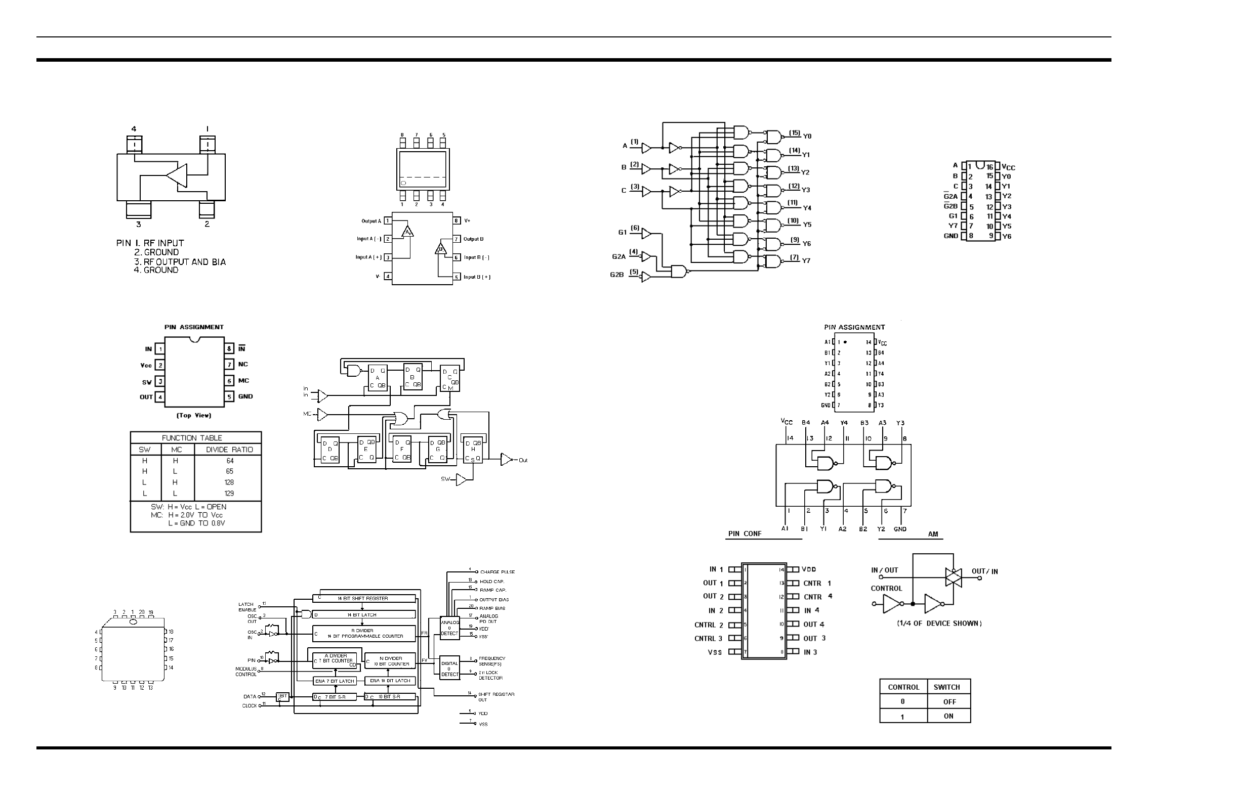
IC DATA
U6
19B80090P5
Synthesizer
U2 thru U4
19A705927P1
Silicon Bipolar IC
U8 & U9
19A702293P3
Dual Operational Amplifier
U5
19A149944P201
Modulus Prescaler
U14
19A702705P4
Quad Analog Switch
U10
19A703471P120
Decoder/Demux
U12 & U13
19A703483P302
Logic Gate/Inverter
LBI-38672J
8
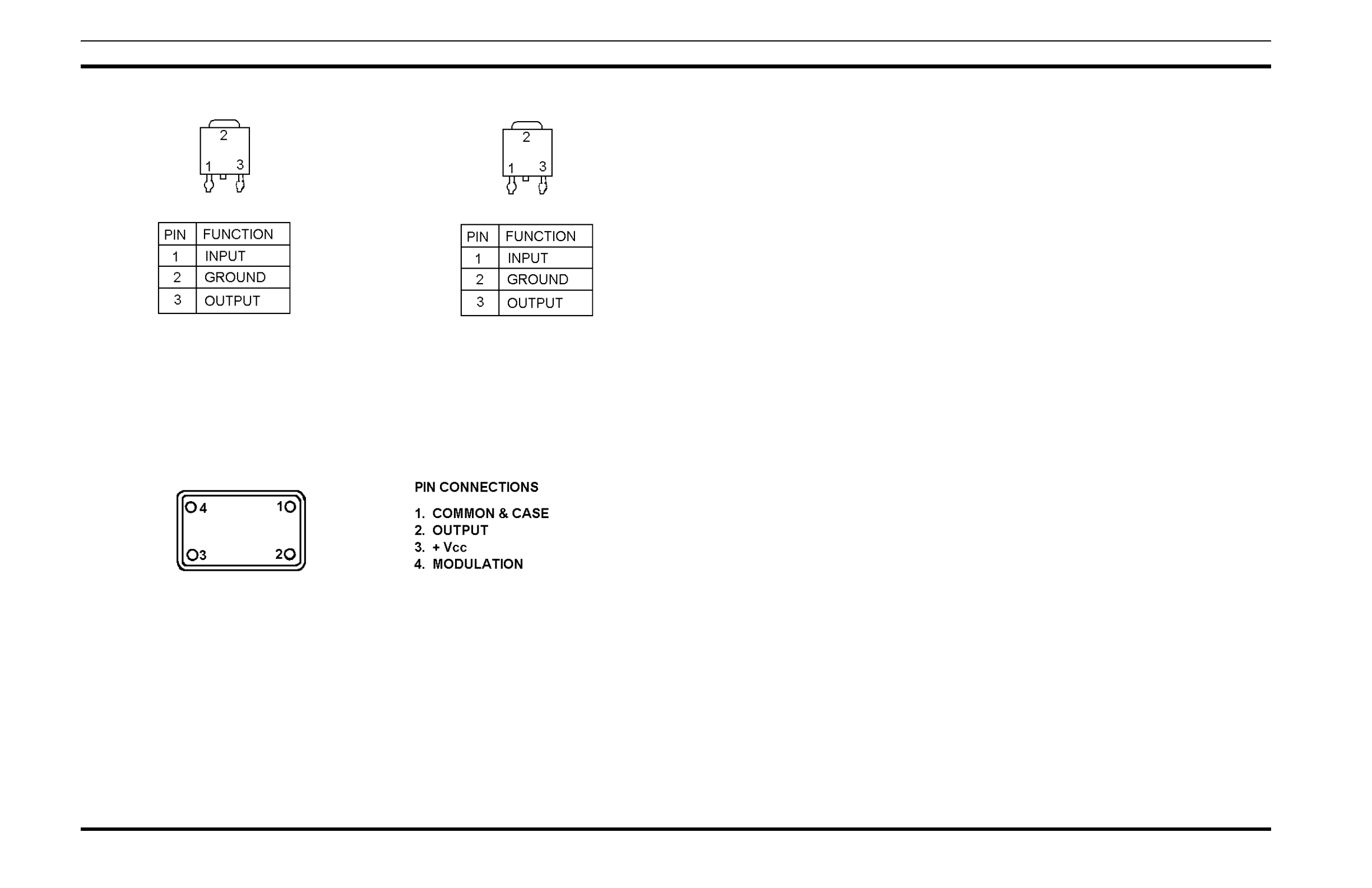
IC DATA
U16
19A704971P10
+8V Regulator
U15
19A704971P8
+5V Regulator
Y1
19B801351P12
Crystal Oscillator
LBI-38672J
9
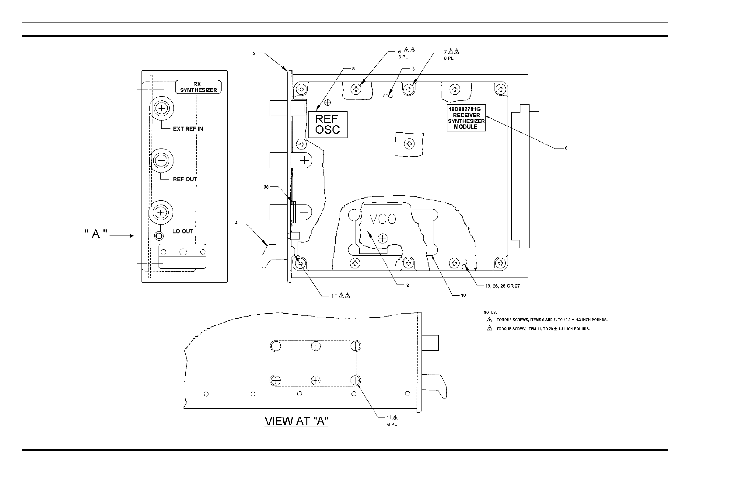
ASSEMBLY DIAGRAM
RECEIVER SYNTHESIZER MODULE
19D902781G3, G7, G8, G10, G12
(19D902781, Sh. 2, Rev. 5)
LBI-38672J
10
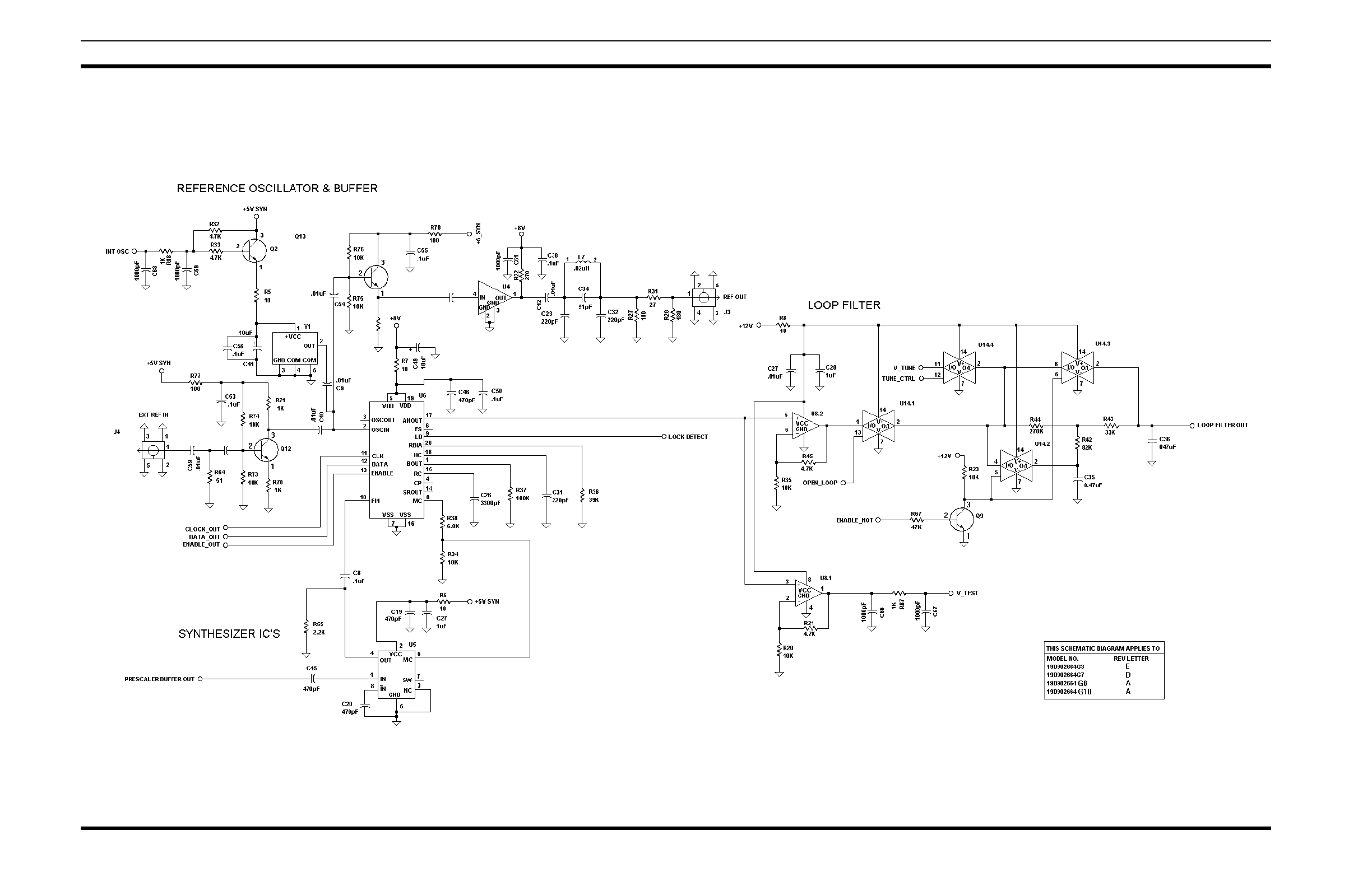
SCHEMATIC DIAGRAM
RECEIVER SYNTHESIZER MODULE
19D902664G3, G7, G8, G10, G12
(19D904091, Sh. 1, Rev. 9A)
LBI-38672J
11
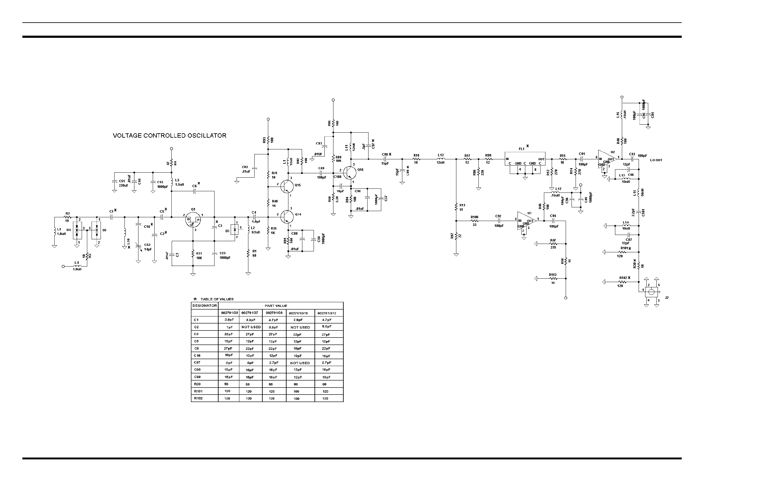
SCHEMATIC DIAGRAM
RECEIVER SYNTHESIZER MODULE
19D902664G3 , G7, G8, G10, G12
(19D904091, Sh. 2, Rev. 9A)
LBI-38672J
12
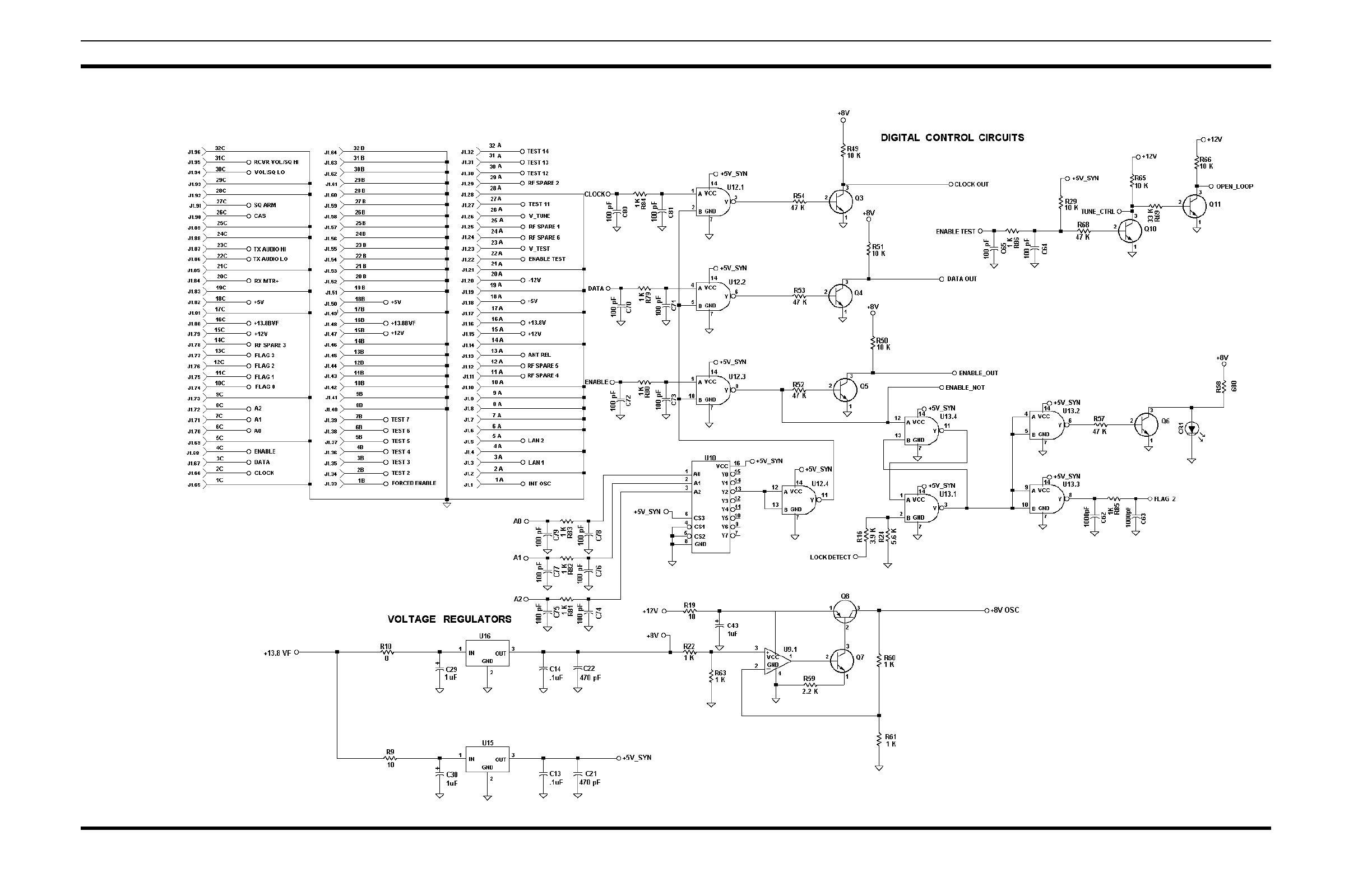
SCHEMATIC DIAGRAM
RECEIVER SYNTHESIZER MODULE
19D902664G3, G7, G8, G10, G12
(19D904091, Sh. 3, Rev. 9A)
LBI-38672J
13

LBI-38673F
TABLE OF CONTENTS
Page
DESCRIPTION . . . . . . . . . . . . . . . . . . . . . . . . . . . . . . . . . . . . . . . . . . . Front Cover
SPECIFICATIONS . . . . . . . . . . . . . . . . . . . . . . . . . . . . . . . . . . . . . . . . . 1
CIRCUIT ANALYSIS
PRESELECTOR FILTER . . . . . . . . . . . . . . . . . . . . . . . . . . . . . . . . . . . 1
PREAMPLIFIER . . . . . . . . . . . . . . . . . . . . . . . . . . . . . . . . . . . . . . . . 1
IMAGE REJECTION FILTER . . . . . . . . . . . . . . . . . . . . . . . . . . . . . . . . . 1
INJECTION AMPLIFIER . . . . . . . . . . . . . . . . . . . . . . . . . . . . . . . . . . . 1
INJECTION FILTER . . . . . . . . . . . . . . . . . . . . . . . . . . . . . . . . . . . . . . 1
DOUBLE BALANCE MIXER . . . . . . . . . . . . . . . . . . . . . . . . . . . . . . . . . 1
FAULT DETECTION . . . . . . . . . . . . . . . . . . . . . . . . . . . . . . . . . . . . . . 1
MAINTENANCE
TEST PROCEDURE . . . . . . . . . . . . . . . . . . . . . . . . . . . . . . . . . . . . . . 2
ALIGNMENT PROCEDURE . . . . . . . . . . . . . . . . . . . . . . . . . . . . . . . . . 2
TROUBLESHOOTING PROCEDURE . . . . . . . . . . . . . . . . . . . . . . . . . . . . 2
BLOCK DIAGRAM . . . . . . . . . . . . . . . . . . . . . . . . . . . . . . . . . . . . . . . . . 1
TABLE 2 - RETUNING . . . . . . . . . . . . . . . . . . . . . . . . . . . . . . . . . . . . . . . 2
PARTS LIST . . . . . . . . . . . . . . . . . . . . . . . . . . . . . . . . . . . . . . . . . . . . . 3
PRODUCTION CHANGES . . . . . . . . . . . . . . . . . . . . . . . . . . . . . . . . . . . . . 4
OUTLINE DIAGRAM . . . . . . . . . . . . . . . . . . . . . . . . . . . . . . . . . . . . . . . 4
ASSEMBLY DIAGRAM . . . . . . . . . . . . . . . . . . . . . . . . . . . . . . . . . . . . . . 6
SCHEMATIC DIAGRAM . . . . . . . . . . . . . . . . . . . . . . . . . . . . . . . . . . . . . . 8
MAINTENANCE MANUAL FOR
RECEIVER FRONT END MODULE
19D902782G3, G4, & G7
DESCRIPTION
The Receiver Front End (RXFE) Module amplifies
and converts the Rf signal to the first IF signal of 21.4
MHz. This is a down conversion process using low side
(G3, G4) or high side (G7) injection. The RXFE module
is powered by a regulated 12 volts. The RXFE printed
wiring board contains the following functional circuits:
•Preselector Filter
•Preamplifier
•Image Rejection Filter
•Injection Amplifier
•Injection Filter
•Double Balanced Mixer
•Fault Detector
All but the Fault Detector circuit in the RXFE mod-
ule have 50 ohm impedance terminations.
E
Ericsson Inc.
Private Radio Systems
Mountain View Road
Lynchburg, Virginia 24502
1-800-592-7711 (Outside USA, 804-592-7711) Printed in U.S.A.
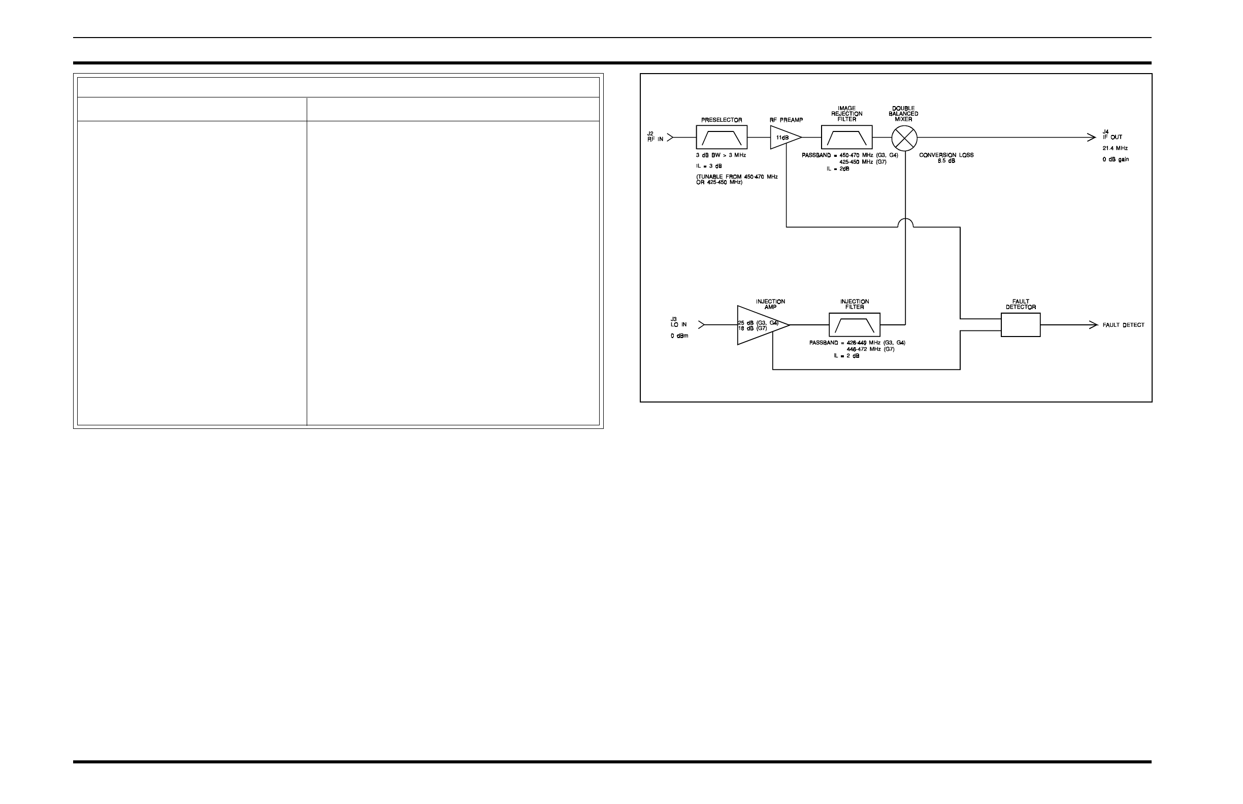
CIRCUIT ANALYSIS
PRESELECTOR FILTER
The received RF signal (J2) is routed through the Prese-
lector Filter. This filter provides front end selectivity and
attenuates the potential spurious signals of first conversion.
Typically, the filter has an insertion loss is 3 dB and an opera-
tional bandwidth of 2 MHz. The filter is primarily a five-pole
helical bandpass filter (L1 thru L5) and is tunable in the band
split MHz range.
PREAMPLIFIER
The output from the Preselector is coupled through an
impedance matching network consisting of L6, C2, and DC
blocking capacitor C1 to the base of Preamplifier Q1. Q1 is a
broadband common emitter amplifier. The Preamplifier stage
is supplied by the regulated +12 Vdc line (VCC1) and draws
about 70 mA through R4. It has a low noise figure and high
Third Order Intercept point. Transistor Q2 provides Q1 with a
constant voltage and current source. The bias on Q1 is moni-
tored by the Fault Detector circuit via R17. Capacitors C20 and
C21 prevent the RF component from entering the fault circuit.
The output signal is coupled to the Image Rejection Filter via
an impedance matching network consisting of C4, L8, and
resistors R5 and R6.
IMAGE REJECTION FILTER
Following the Preamplifier is the Image Rejection Filter.
The Image Rejection Filter is a fixed tuned helical bandpass
filter and can meet the desired image rejection of the frequency
band.
INJECTION AMPLIFIER
The local oscillator input (J3) from the Receiver Synthe-
sizer is coupled through an impedance matching network (C5
and L9) to the base of the Injection Amplifier Q3. Q3 and Q8
are common emitter amplifiers. The output from Q3 is coupled
through an impedance matching network (C6, C7, and L11) to
the base of Q8. The Injection Amplifier, consisting of Q3, Q8,
and associated circuitry, is capable of amplifying the injection
signal from 0 dBm to +25 dBm in the 428 to 449 MHz range
or to +18 dBm in the 446-472 MHz range. The amplifier is
powered by the regulated +12 Vdc line (VCC1). Transistors
Q4 and Q7 provide Q3 and Q8 with a constant voltage and
current source. The bias on Q3 and Q8 is monitored by the
Fault Detector circuit via R21 and R31, respectively. Capaci-
tors C22, C23 and C26 prevent the RF component from
entering the fault circuit. The output signal is coupled to the
Injection Filter via an impedance matching network consist-
ing of C8, L13, and resistors R15 and R16.
INJECTION FILTER
Following the Injection Amplifier is the Injection Filter
consisting of C9 through C19, L14 through L20, and R30.
Configured as a bandpass filter, the Injection Filter has a
bandwidth of 428 to 450 MHz (G3, G4) or 446 to 472 MHz
(G7) and is used to attenuate the harmonics of the Injection
Amplifier. The filter also has an insertion loss of about 2 dB.
DOUBLE BALANCE MIXER
The Double Balance Mixer (DBM) is a broadband
mixer. It converts an RF signal to the 21.4 MHz first conver-
sion IF frequency. The mixer uses low side (G3, G4) or high
side (G7) injection driven by a local oscillator signal of +20
(G3, G4) or +15 (G7) dBm. The mixer conversion loss is
typically about 6.5 dB. The IF output signal is then routed to
the output connector (J4).
FAULT DETECTOR
The Fault Detector circuit monitors the operation of
preamplifier and injection amplifier devices. Operational
amplifiers U1.1 and U1.2 compare the bias on the Preampli-
fier Q1 to preset levels, while U1.3 and U1.4 compare the
bias levels on Injection Amplifiers Q3 and Q8.
When the bias for Q1, Q3, and Q8 is within the preset
window limits, the output from the comparators is a high
level. This causes Q5 to conduct, turning off Q6 and the fault
indicator, CR2. A high level signal is also sent to the Con-
troller on the FLAG 0 line.
Copyright© July 1992, Ericsson GE Mobile Communications, Inc.
Table 1 - General Specifications
ITEM SPECIFICATION
FREQUENCY RANGE 450.0 MHz - 470.0 MHz (G3, G4)
425.0 MHz - 470.0 MHz (G7)
IF FREQUENCY 21.4 MHz
3 dB BANDWIDTH >3 MHz
IMPEDANCE 50 ohms at RF, LO, and IF Ports
CONVERSION LOSS -2 dB ±1 dB
NOISE FIGURE (NF) <7.5 dB
THIRD ORDER INTERCEPT POINT >+20 dBm (G3, G4)
>+15 dBm (G7)
IMAGE REJECTION >100dB
INJECTION POWER +2 dBm ±2 dB
TEMPERATURE RANGE -30°C TO +60°C
SUPPLY VOLTAGE 12.0 Vdc
SUPPLY CURRENT 290 mA ±20 mA typical
230 mA ±20 mA typical (G3) Figure 1 - Block Diagram
LBI-38673F
1
If the biasing for the amplifiers is not within the proper
operating range, the fault detector circuit will pull the FLAG
0 line low. This turns off Q5 causing Q6 to conduct. Q6 now
provides a ground path for CR2, turning on the fault indica-
tor.
MAINTENANCE
TEST PROCEDURE
The RXFE module has to be tested for Noise Figure,
Gain, Third Order Intercept Point, Isolation etc.. With proper
current drawing of devices, Bandwidth and Conversion Gain
the RXFE module will meet its specifications. The following
are test procedures will verify proper Conversion Gain and
current drain:
1. Supply 12 Vdc to pin 15A, B, C. (1C is ground.)
2. Inject the desired RF signal into RF IN at a level of
-10 dBm.
3. Inject the desired local oscillator signal into LO IN
at a level of 0 dBm [LO frequency = RF frequency -
21.4 MHz (G3, G4) + 21.4 MHz (G7)].
4. Measure the IF OUT power at 21.4 MHz, the ratio of
RF IN to IF OUT is -2 dB ±1 dB.
5. Measure the current drawn by the RXFE module.
Typical current drain is 290 mA.
ALIGNMENT PROCEDURE
Alignment for the Receiver Front End module consists
of tuning the five-pole Preselector Filter only. Normally, the
RXFE should only need the fine-tuning procedures. For a
major receiver frequency change, the RXFE needs to be
adjusted using the major-retuning procedures.
For Fine-Tuning
1. Supply 12 Vdc to pin 15A, B, C. (1C is ground.)
2. Inject the desired RF signal into RF IN (J2) at a level
of -10 dBm.
3. Inject the desired local oscillator signal into LO IN
(J3) at a level of 0 dBm [LO frequency = RF fre-
quency - 21.4 MHz (G3, G4) + 21.4 MHz (G7)].
4. Detect IF signal at 21.4 MHz. Slightly adjust L1 to
L5 to get maximum power (don’t adjust more than
ten degrees). If an RF Voltmeter is used, connect a
Low Pass Filter (LPF)to the IF OUT (J4) to attenuate
high frequency components. The corner of the LPF
should be set for 40 MHz.
5. Repeat Test Procedure steps to verify conversion
gain and current drain.
For Major Retuning
The best way to do a major retuning of the RXFE is with
swept frequency tuning. The swept frequency tuning can be
done using a Spectrum Analyzer and Tracking Generator.
With proper Injection power and current drain, the frequency
response of the Preselector Filter can be seen by viewing the
RF to IF port feedthrough on the spectrum analyzer. This
feedthrough is typically 35 dB down from the input level at
the RF port. Use the following procedure for swept fre-
quency tuning:
1. Supply 12 Vdc to pin 15A, B, C. (1C is ground.)
2. Inject the Tracking generator output at 0 dBm into
the RF IN connector, (J2).
3. Inject local oscillator power at 0 dBm into the LO IN
connector, (J3) [LO frequency = RF frequency - 21.4
MHz (G3, G4) + 21.4 MHz (G7)].
4. Preset the height of slugs with respect to the top of
five-pole cavity as follows (Table 2):
Table 2
5. Center the spectrum analyzer at the desired frequency
and set the reference at about -30 dBm. Adjust L1 to
L5 for best possible response.
HEIGHT (in inches)
Frequency
(MHz)L1 L2L3L4L5
450 15/64 16/64 17/64 17/64 16/64
454 16/64 17/64 17/64 18/64 15/64
458 16/64 19/64 19/64 19/64 17/64
462 18/64 19/64 20/64 20/64 18/64
466 21/64 22/64 23/64 21/64 20/64
470 22/64 24/64 24/64 23/64 22/64
SYMPTOM AREAS TO CHECK READING (TYP.)
LOW CONVERSION GAIN Check Vcc 12 V
Preselector Loss 3.5 dB
Preamplifier Gain 11 dB
Image Rej. Filter Loss 2 dB
1st Mixer Conversion Loss 6.5 dB
1 L.O. Level (@ mixer L.O. +22 ±2 dBm (G3, G4)
port) +14 ±2 dBm (G7)
LED INDICATOR ON Check Vc of Q1 10 V
Check Vc of Q3 and Q8 10 V
IF FREQUENCY OFF Check L.O. FREQUENCY L.O. frequency = RF frequency - 21.4 MHz (G3,G4)
+ 21.4 MHz (G7)
LOW L.O. POWER* Injection Amplifier Gain 23 ±2 dB (G3, G4)
18 ±2 dB (G7)
Injection Filter Loss 2 dB
*NOTE: For troubleshooting the gain or loss, the RXFE needs to be under the normal operating condition:
•12 Vdc supply.
•Inject L.O. power at a level of 0 dBm into LO IN (J3), [LO freq. = RF freq. - 21.4 MHz (G3, G4)
+ 21.4 MHz (G7).
•Inject the desired RF signal at a level of -10 dBm into RF IN (J2).
•Terminate the IF OUT (J4) with a good 50 ohm impedance.
•Use a Spectrum Analyzer and 50 ohm probe (with good RF grounding) to probe at the input and output of
each stage to check its gain or loss (see schematic diagram).
TROUBLESHOOTING GUIDE
LBI-38673F
2
RECEIVER FRONT END MODULE
19D902782G3 (450-470 MHz)
19D902782G4 (450-470 MHz ETSI)
19D902782G7 (425-450 MHz)
ISSUE 5
PARTS LIST
SYMBOL PART NUMBER DESCRIPTION
4 19D902555P1 Handle.
5 19D902534P1 Cover, RF.
6 19A702381P506 Screw, thread forming: TORX, No.
M3.5-.6 x 6.
7 19A702381P513 Screw, thread forming: TORX, No.
M3.5-0.6 X 13.
11 19A702381P508 Screw, thd. form: No. 3.5-0.6 x 8.
RECEIVER FRONT END BOARD
19D902490G3 (450-470 MHz)
19D902490G4 (450-470 MHz ETSI)
19D902490G7 (425-450 MHz)
— — — — CAPACITORS — — —
C1 19A702052P14 Ceramic: 0.01 µF ± 10%, 50 VDCW.
C2 19A702061P17 Ceramic: 12 pF ±5%, 50 VDCW, temp
coef 0 ± 30 PPM.
C3 19A702052P14 Ceramic: 0.01 µF ± 10%, 50 VDCW.
C4 19A702061P12 Ceramic: 8.2 pF ± 0.5 pF, 50 VDCW,
temp coef 0 ± 60 PPM. (Used in G3, G4).
C4 19A702061P61 Ceramic: 100pF,±5%, 50VDCW,
temp coef 0±30 PPM/°C. (Used in G7).
C5 19A702061P17 Ceramic: 12 pF ±5%, 50 VDCW, temp
coef 0 ± 30 PPM.
C6 19A702061P57 Ceramic: 82 pF ±5%, 50 VDCW, temp
coef 0 ± 30 PPM. (Used in G3, G4).
C6 19A702061P63 Ceramic: 120 pf,±5%, 50VDCW,
temp coef 0±30 PPM/°C. (Used in G7).
C7 19A702061P17 Ceramic: 12 pF ±5%, 50 VDCW, temp
coef 0 ± 30 PPM. (Used in G3, G4).
C7 19A702061P10 Ceramic: 5.6 pF, 0.5 pF, 50VDCW,
temp coef 0±60 PPM/°C. (Used in G7).
C8 19A702061P29 Ceramic: 22 pF ±5%, 50 VDCW, temp
coef 0 ± 30 PPM. (Used in G3, G4).
C8 19A702061P63 Ceramic: 120 pF,±5%, 50VDCW,
temp coef 0±30 PPM. (Used in G7).
C9 19A702061P13 Ceramic: 10 pF ±5%, 50 VDCW, temp
coef 0 ± 30 PPM. (Used in G3, G4).
C9 19A702061P17 Ceramic: 12 pF, ±5%, 50VDCW,
temp coef 0±30 PPM. (Used in G7).
C10 19A702061P11 Ceramic: 6.8 pF ± 0.5 pF, 50 VDCW,
temp coef 0 ± 60 PPM. (Used in G3, G4).
C10 19A702061P21 Ceramic: 15 pF,±5%, 50VDCW,
temp coef 0±30 PPM. (Used in G7).
C11 19A702061P12 Ceramic: 8.2 pF ± 0.5 pF, 50 VDCW,
temp coef 0 ± 60 PPM. (Used in G3, G4).
C11 19A702061P25 Ceramic: 18 pF,±5%, 50VDCW,
temp coef 0±30 PPM. (Used in G7).
C12 19A702061P13 Ceramic: 10 pF ±5%, 50 VDCW, temp
and coef 0 ± 30 PPM. (Used in G3, G4).
C13
C12 19A702061P21 Ceramic: 15 pF,±5%, 50VDCW,
temp coef 0±30 PPM. (Used in G7).
*COMPONENTS, ADDED, DELETED OR CHANGED BY PRODUCTION CHANGES
SYMBOL PART NUMBER DESCRIPTION
— — — — — JACKS — — — —
J1 19B801587P7 Connector, DIN: 96 male contacts, right
angle mounting; sim to AMP 650887-1.
J2 19A115938P24 Connector, receptacle.
thru
J4
— — — — INDUCTORS — — —
L1 19C850817P10RF Coil: sim to Paul Smith SK853-1.
(Used in G3, G4).
L1 19C850817P25 Coil. (Used in G7).
L2 19C850817P9 RF Coil: sim to Paul Smith SK853-1.
thru (Used in G3, G4).
L4
L2 19C850817P5 Coil. (Used in G7).
thru
L4
L5 19C850817P10 RF Coil: sim to Paul Smith SK853-1.
(Used in G3, G4).
L5 19C850817P25 Coil. (Used in G7).
L6 19A705470P3 Coil, Fixed: 15 nH; sim to Toko
380NB-15nM.
L7 19A705470P16 Coil, Fixed: 0.18 µH; sim to Toko
380NB-R18M.
L8 19A705470P7 Coil, fixed: 33 nH ±20%; sim to Toko
380NB-33nM.
L9 19A705470P5 Coil, Fixed: 22 nH; sim to Toko
380NB-22nM. (Used in G3, G4).
L9 19A705470P3 Coil, fixed: 15 nH; sim to Toko
380NB-15nM. (Used in G7).
L10 19A705470P16 Coil, Fixed: 0.18 µH; sim to Toko
380NB-R18M.
L11 19A705470P3 Coil, Fixed: 15 nH; sim to Toko
380NB-15nM. (Used in G3, G4).
L11 19A705470P5 Coil, fixed: 22 nH: sim to Toko
380NB-22nM. (Used in G7).
L12 19A705470P16 Coil, Fixed: 0.18 µH; sim to Toko
380NB-R18M.
L13 19A705470P6 Coil, Fixed: 27 nH; sim to Toko
380NB-27nM. (Used in G3, G4).
L13 19A705470P8 Coil, fixed: 39 nH; sim to Toko
380NB-35nM. (Used in G7).
L14 19A705470P4 Coil, Fixed: 18 nH; sim to Toko
380NB-18nM. (Used in G3, G4).
L15 19A705470P7 Coil, fixed: 33 nH ±20%; sim to Toko
380NB-33nM. (Used in G3, G4).
L14 19A705470P1 Coil, fixed: 10 nH; sim to Toko
and 380NB-10nM. (Used in G7).
L15
L16 19A705470P5 Coil, Fixed: 22 nH; sim to Toko
and 380NB-22nM. (Used in G3, G4).
L17
L16 19A705470P2 Coil, fixed: 12 nH; sim to Toko
and 380NB-12 nM. (Used in G7).
L17
L18 19A705470P1 Coil, Fixed: 10 nH; sim to Toko
380NB-10nM. (Used in G3, G4).
L18 19A705470P3 Coil, fixed: 15 nH; sim to Toko
380NB-15nM. (Used in G7).
L19 19A705470P3 Coil, fixed: 15 nH; sim to Toko
380NB-15nM.
L20 19A705470P24 Coil, Fixed: 0.82 µH; sim to Toko
380NB-R82M.
SYMBOL PART NUMBER DESCRIPTION
C13 19A702061P13 Ceramic: 10 pF,±5%, 50VDCW,
temp coef 0±30 PPM.
C14 19A702061P8 Ceramic: 3.9 pF ± 0.5 pF, 50 VDCW,
temp coef 0 ± 120 PPM.
(Used in G3, G4).
C14 19A702061P7 Ceramic: 3.3 pF, 0.5 pF, 50VDCW,
temp coef 0±120 PPM. (Used in G7).
C15 19A702061P11 Ceramic: 6.8 pF ± 0.5 pF, 50 VDCW,
temp coef 0 ± 60 PPM. (Used in G3, G4).
C15 19A702061P69 Ceramic: 220 pF,±5%, 50VDCW,
temp coef 0±30 PPM. (Used in G7).
C16 19A702061P8 Ceramic: 3.9 pF ± 0.5 pF, 50 VDCW,
temp coef 0 ± 120 PPM.
(Used in G3, G4).
C16 19A702061P7 Ceramic: 3.3 pF, 0.5 pF, 50VDCW,
temp coef 0±120 PPM. (Used in G7).
C17 19A702061P9 Ceramic: 4.7 pF ± 0.5 pF, 50 VDCW,
temp coef 0 ± 60 PPM. (Used in G3, G4).
C17 19A702061P69 Ceramic: 220 pF,±5%, 50VDCW,
temp coef 0±30 PPM. (Used in G7).
C18 19A702061P8 Ceramic: 3.9 pF ± 0.5 pF, 50 VDCW,
temp coef 0 ± 120 PPM.
(Used in G3, G4).
C18 19A702061P7 Ceramic: 3.3 pF, 0.5 pF, 50VDCW,
temp coef 0±30 PPM. (Used in G7).
C19 19A702061P45 Ceramic: 47 pF ±5%, 50 VDCW, temp
coef 0 ±30 PPM.
C20 19A702052P14 Ceramic: 0.01 µF ± 10%, 50 VDCW.
thru
C28
C29 19A702061P89 Ceramic: 1500 pF, ±5%, 50VDCW,
and temp coef 0±120 PPM.
C30 (Used in G4 & G7).
*C29 19A705205P26 Tantalum: 3.3 µF ±20%, 16VDCW,
and (Used in G3).
*C30
*C31 19A705205P15 Tantalum: 33 µF ±20%, 16VDCW,
and (Used in G3).
*C32
C31 19A702236P40 Ceramic: 39 pF, ±5%, 50VDCW,
thru temp coef 0±30 PPM. (Used in G4 & G7).
C33
C34 19A702061P37 Ceramic: 33 pF,±5%, 50VDCW,
thru temp coef 0±30 PPM. (Used in G4 & G7).
C36
*C37 19A705205P26 Tantalum: 3.3 µF ±20%, 16VDCW,
and (Used in G4, G7).
*C38
*C39 19A705205P15 Tantalum: 33 µF ±20%, 16VDCW,
and (Used in G4, G7).
*C40
— — — — DIODES — — — — —
CR1 344A3062P1 Diode, Schotty (part of 19D902782G3).
CR2 19A703595P10 Diode, Optoelectric: Red; sim to HP
HLMP-1301-010. (Used in G3).
— — — — FILTERS— — — — —
FL1 19A705458P1 Helical, UHF: 450-470 MHz.
(Used in G3, G4).
FL1 19A705458P5 Helical, UHF: 425-450 MHz.
(Used in G7).
SYMBOL PART NUMBER DESCRIPTION
L21 19A705470P16 Coil, Fixed: 0.18 µH; sim to Toko
380NB-R18M.
L22 19A700021P105 Coil, RF ceramic: 22 nH. (Used in G4).
L22 19A705470P6 Coil, fixed: 27 nH; sim to Toko
380NB-27nM. (Used in G7).
L23 19A700021P13 Coil, RF ceramic: 470 nH. (Used in G4).
L23 19A705470P21 Coil, fixed: 0.47 uH; sim to Toko
380NB-R47M. (Used in G7).
*L24 19A700000P122 Coil, fixed: 8.2 uH ± 10%; sim to
Jeffers 22-8.2-10.
— — — — TRANSISTORS— — — —
Q1 344A3058P1 Silicon, NPN.
Q2 19A700059P2 Silicon, PNP: sim to MMBT3906, low
profile.
Q3 19A704708P3 Silicon NPN.
Q4 19A700059P2 Silicon, PNP: sim to MMBT3906, low
profile.
Q5 19A700076P2 Silicon, NPN: sim to MMBT3904, low
and profile. (Used in G3).
Q6
Q7 19A700059P2 Silicon, PNP: sim to MMBT3906, low
profile.
Q8 344A3058P1 Silicon, NPN.
— — — — RESISTORS — — — —
R1 19B800607P183 Metal film: 18K ohms ±5%, 1/8 w.
R2 19B800607P102 Metal film: 1K ohms ±5%, 1/8 w.
R3 19B800607P331 Metal film: 330 ohms ±5%, 1/8 w.
R4 19B800607P270 Metal film: 27 ohms ±5%, 1/8 w.
R5 19B800607P100 Metal film: 10 ohms ±5%, 1/8 w.
(Used in G3, G4).
R5 19B800607P1 Metal film: 0 ohms. (Used in G7).
R6 19B800607P391 Metal film: 390 ohms ±5%, 1/8 w.
(Used in G3, G4).
R7 19B800607P183 Metal film: 18K ohms ±5%, 1/8 w.
R8 19B800607P682 Metal film: 6.8K ohms ±5%, 1/8 w.
R9 19B800607P182 Metal film: 1.8K ohms ±5%, 1/8 w.
R10 19B800607P470 Metal film: 47 ohms ±5%, 1/8 w.
(Used in G3).
R10 19B800607P221 Metal film: 220 ohms ±5%, 1/8w.
(Used in G4).
R11 19B800607P331 Metal film: 330 ohms ±5%, 1/8 w.
R12 19B800607P562 Metal film: 5.6K ohms ±5%, 1/8 w.
R13 19B800607P122 Metal film: 1.2K ohms ±5%, 1/8 w.
R14 19B800607P180 Metal film: 18 ohms ±5%, 1/8 w.
(Used in G3, G4).
R14 19B800607P270 Metal film: 27 ohms ±5%, 1/8 w
(Used in G7).
R15 19B800607P270 Metal film: 27 ohms ±5%, 1/8 w.
R16 19B800607P181 Metal film: 180 ohms ±5%, 1/8 w.
R17 19B800607P103 Metal film: 10K ohms ±5%, 1/8 w.
R18 19B800607P562 Metal film: 5.6K ohms ±5%, 1/8 w.
R19 19B800607P183 Metal film: 18K ohms ±5%, 1/8 w.
R20 19B800607P333 Metal film: 33K ohms ±5%, 1/8 w.
R21 19B800607P103 Metal film: 10K ohms ±5%, 1/8 w.
R22 19B800607P822 Metal film: 8.2K ohms ±5%, 1/8 w.
LBI-38673F
3
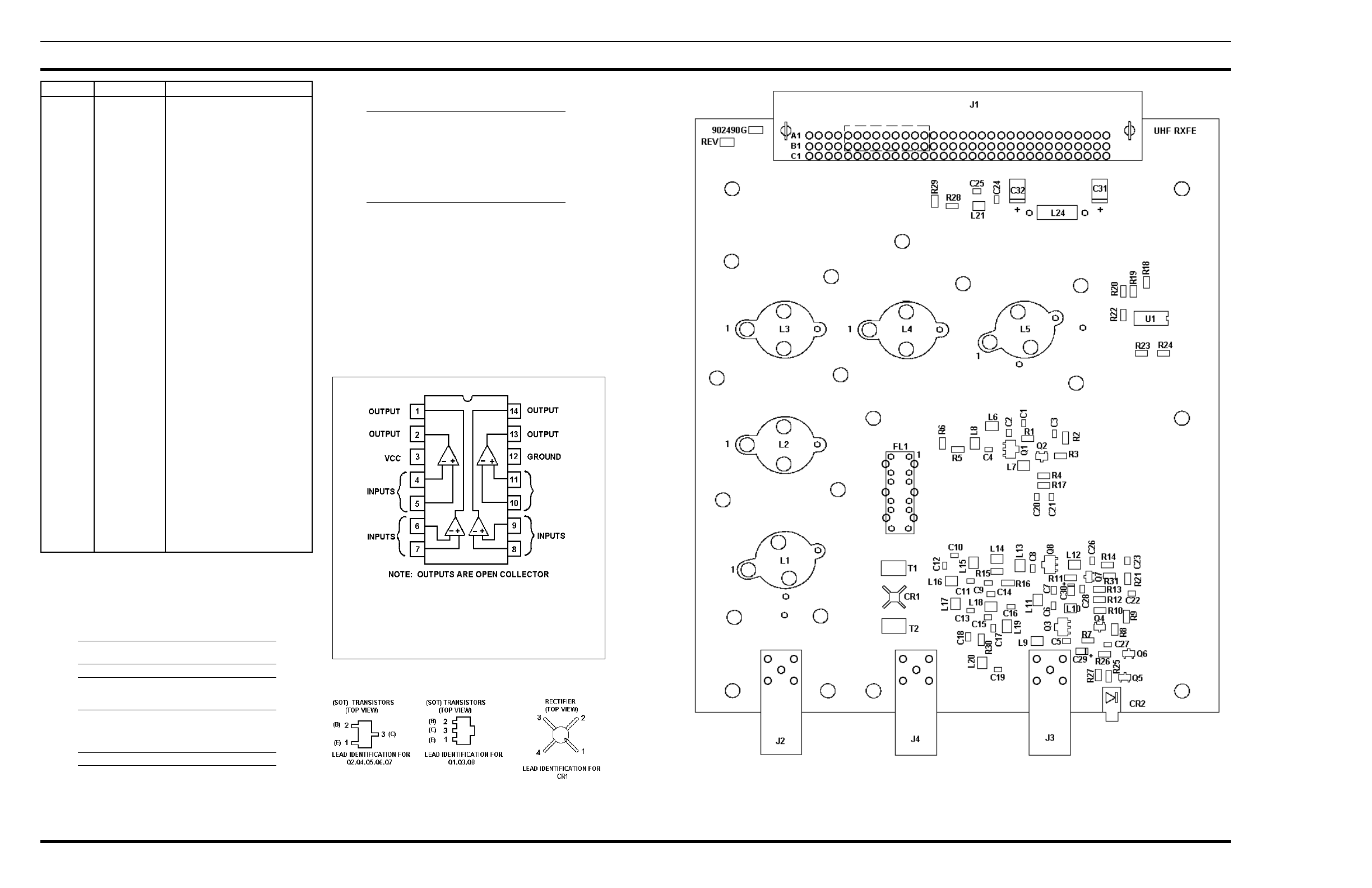
OUTLINE DIAGRAM
PARTS LIST & PRODUCTION CHANGES
SYMBOL PART NUMBER DESCRIPTION
R23 19B800607P333 Metal film: 33K ohms ±5%, 1/8 w.
and
R24
R25 19B800607P104 Metal film: 100K ohms ±5%, 1/8 w.
(Used in G3).
R26 19B800607P273 Metal film: 27K ohms ±5%, 1/8 w.
(Used in G3).
R27 19B800607P391 Metal film: 390 ohms ±5%, 1/8 w.
(Used in G3).
R28 19B800607P103 Metal film: 10K ohms ±5%, 1/8 w.
R29 19B800607P682 Metal film: 6.8K ohms ±5%, 1/8 w.
R30 19B800607P470 Metal film: 47 ohms ±5%, 1/8 w.
R31 19B800607P103 Metal film: 10K ohm,±5%, 1/8w.
R32 19B800607P560 Metal film: 56 ohms,±5%, 1/8w.
R33 19B800607P510 Metal film: 51 ohms,±5%, 1/8w.
(Used in G7).
R34 19B801251P1 Metal film: 0 ohms.
R35 19B800607P270 Metal film: 27 ohms,±5%, 1/8w.
(Used in G7).
— — — TRANSFORMERS — —
T1 344A3063P1 Transformer.
and
T2
— — INTEGRATED CIRCUITS —
U1 19A704125P1 Linear: Quad Comparator; sim to
LM339D.
— — — MISCELLANEOUS — —
20 19B800701P2 Tuning screw.
21 19A701800P1 Stop nut.
22 19D902467P2 Casting.
28 19D902534P2 Cover, RF. (Used in G4).
29 19D904572P1 Cover, Gasket. (Used in G4).
30 19B802690P1 Grommet. (Used in G4).
U1
19A704125P1
Quad Operational Amplifier
(19D902490, Sh. 3, Rev. 5)
RECEIVER FRONT END BOARD
19D902490G3
PRODUCTION CHANGES - CONT.
REV. B - RECEIVER FRONT END BOARD 19D902490G7
To improve receiver sensitivity L8 changed from
18nH (19A705470P4) to 33nH (19A705470P7);
R5 changed from 10 ohms (19B800607P100)
to 0 ohms (19B800607P1);
R14 changed from 18 ohms (19B800607P180)
to 27 ohms (19B800607P270);
R6 (19B800607P391) and R36 (19B800607P391)
were deleted.
REV. D - RECEIVER FRONT END BOARD 19D902490G3
Reduce excessive LO drive level. Changed R15 from
10 ohms (19B800607P100) to 27 ohms (19B800607P270).
Changed R16 from 390 ohms (19B800607P391) to
180 ohms (19B800607P181).
PRODUCTION CHANGES
Changes in the equipment to improve or to simplify circuits are
identified by a "Revision Letter", which is stamped after the model
number of the unit. The revision stamped on the unit includes all
previous revisions. Refer to the Parts List for descriptions of parts
affected by these revisions.
REV. A - RECEIVER FRONT END BOARD 19D902490G3
Upgrade to ETSI specs. New PWB.
REV. B - RECEIVER FRONT END BOARD 19D902490G3
REV. A - RECEIVER FRONT END BOARD 19D902490G4
To correct overheating problem.
R14 was 10 ohms (19B800607P100).
REV. C - RECEIVER FRONT END BOARD 19D902490G3
To eliminate receiver spurious response at 100 kHz
switching power supply frequency.
Added C29, C30, C31, C32 and L24.
REV. B - RECEIVER FRONT END BOARD 19D902490G4
REV. A - RECEIVER FRONT END BOARD 19D902490G7
To eliminate receiver spurious response at 100 kHz
switching power supply frequency.
Added C37, C38, C39, C40 and L24.
LBI-38673F
4
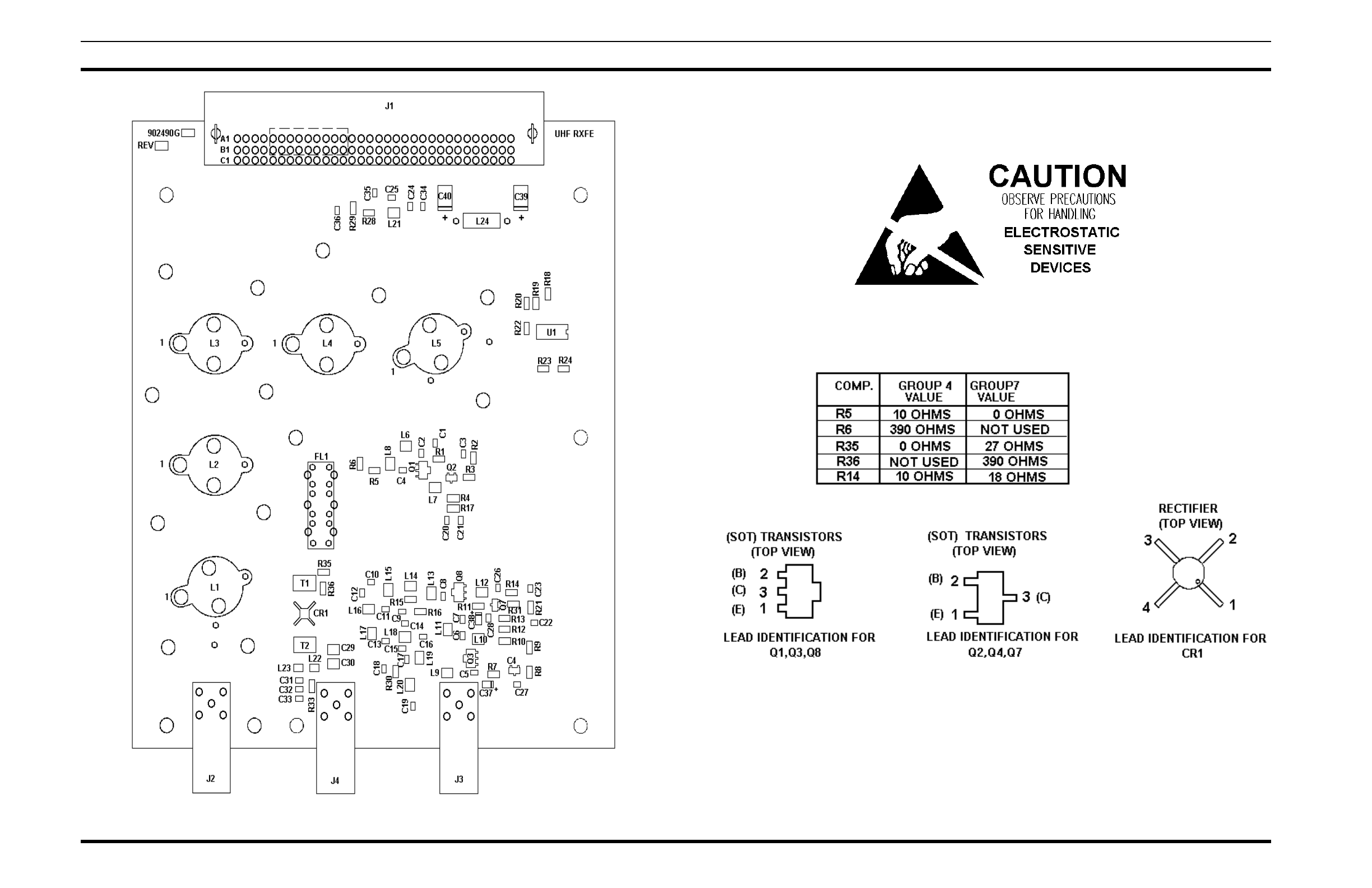
RECEIVER FRONT END BOARD
19D902490G4 & G7
OUTLINE DIAGRAM
(19D902490, Sh. 4, Rev. 6A)
LBI-38673F
5
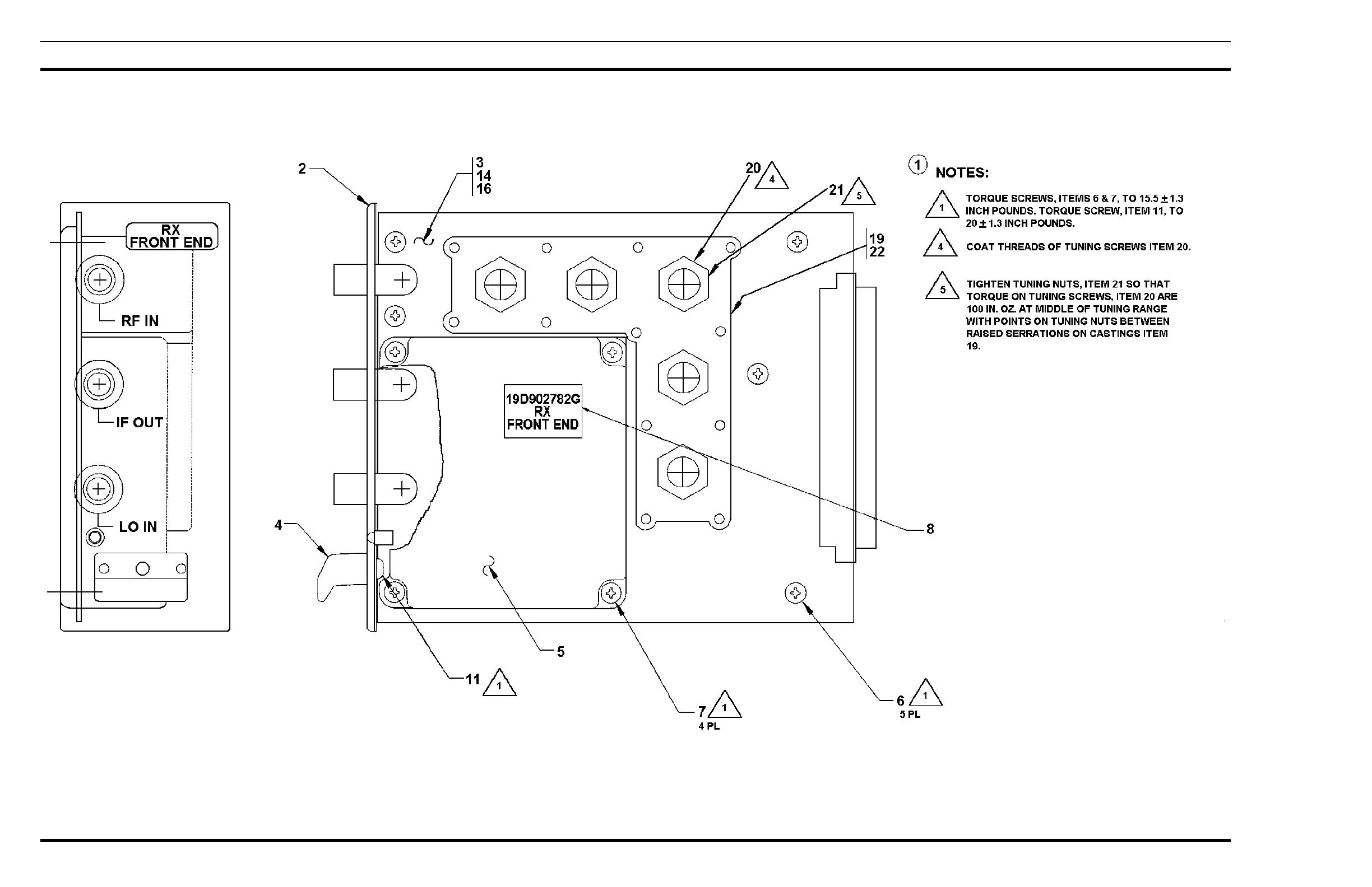
ASSEMBLY DIAGRAM
RECEIVER FRONT END MODULE
19D902782G3
(19D902782 Sh.1 Rev. 6)
LBI-38673F
6
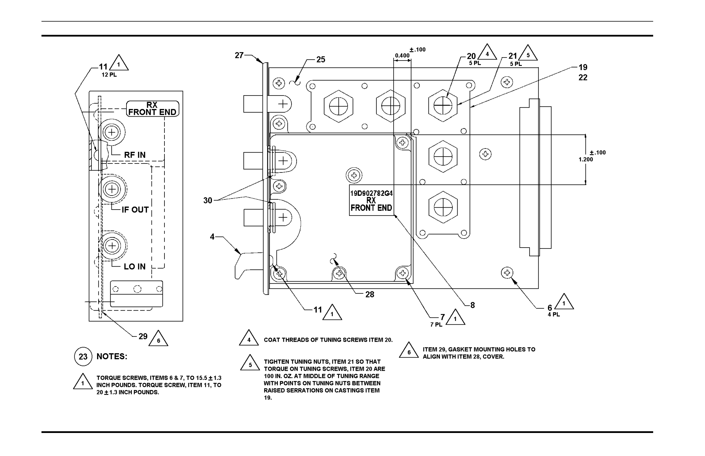
ASSEMBLY DIAGRAM
RECEIVER FRONT END MODULE
19D902782G4 & G7
(19D902782 Sh.2 Rev. 6)
LBI-38673F
7
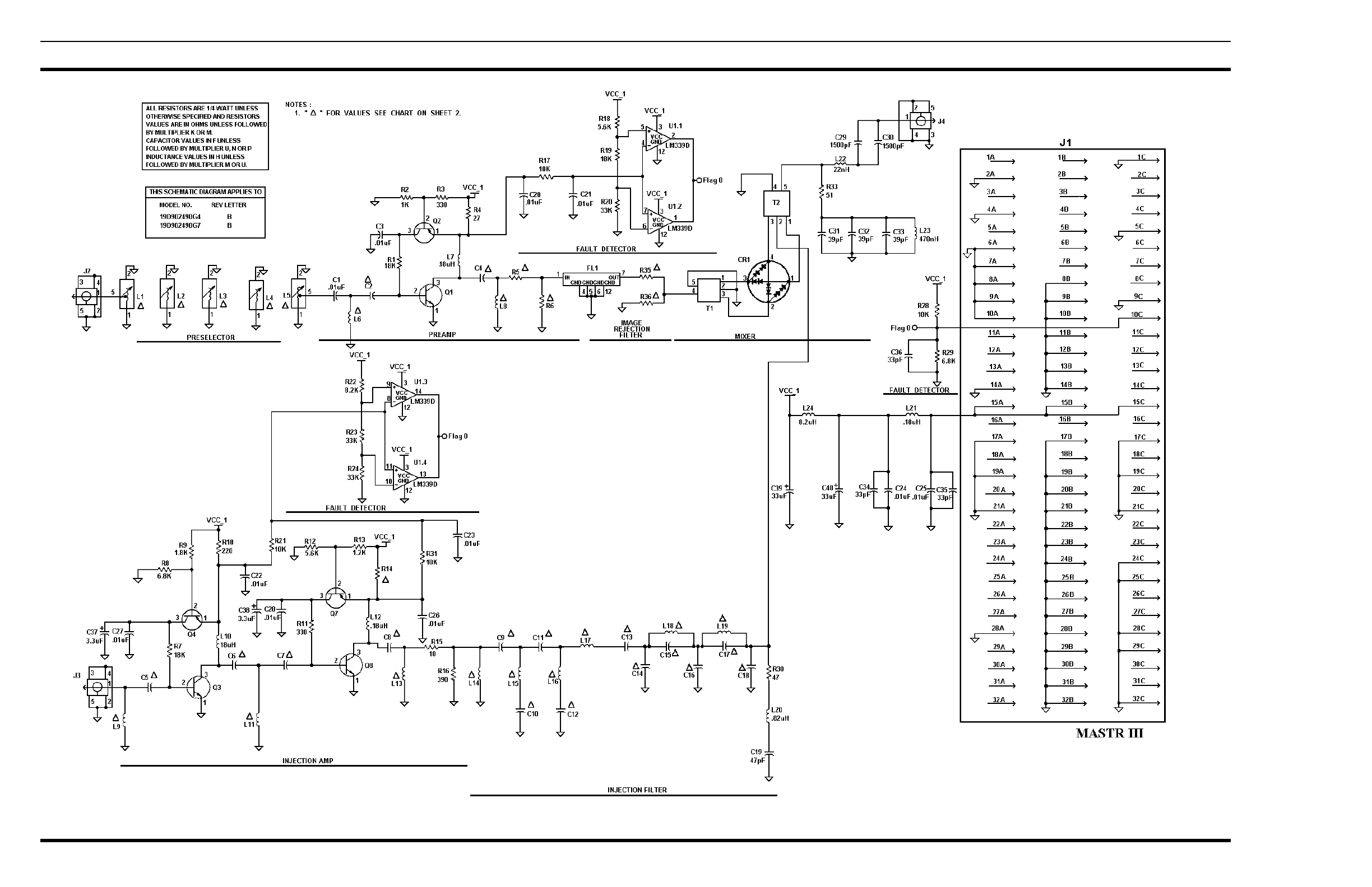
SCHEMATIC DIAGRAM
RECEIVER FRONT END MODULE
19D902782G4 & G7
(19D904768 Sh.1 Rev. 6)
LBI-38673F
8
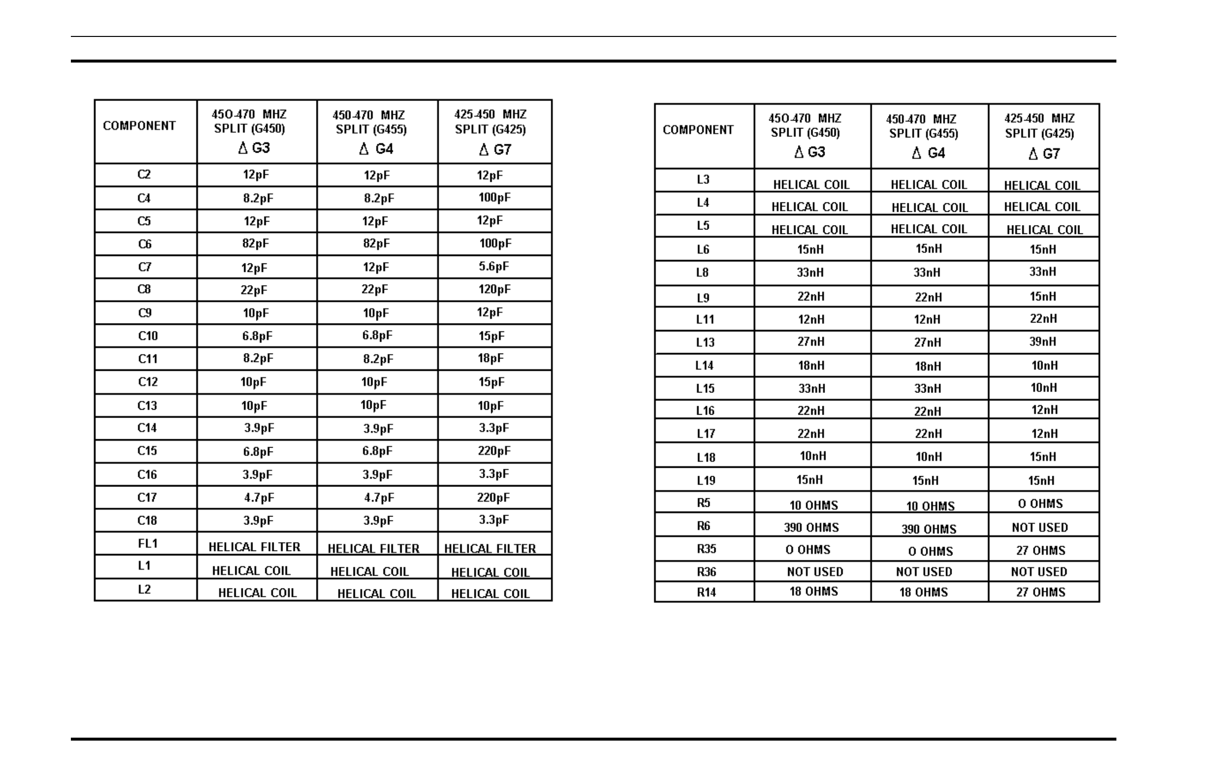
SCHEMATIC DIAGRAM
RECEIVER FRONT END MODULE
19D902782G3,G4 & G7
(19D904768 Sh.2 Rev. 6)
LBI-38673F
9
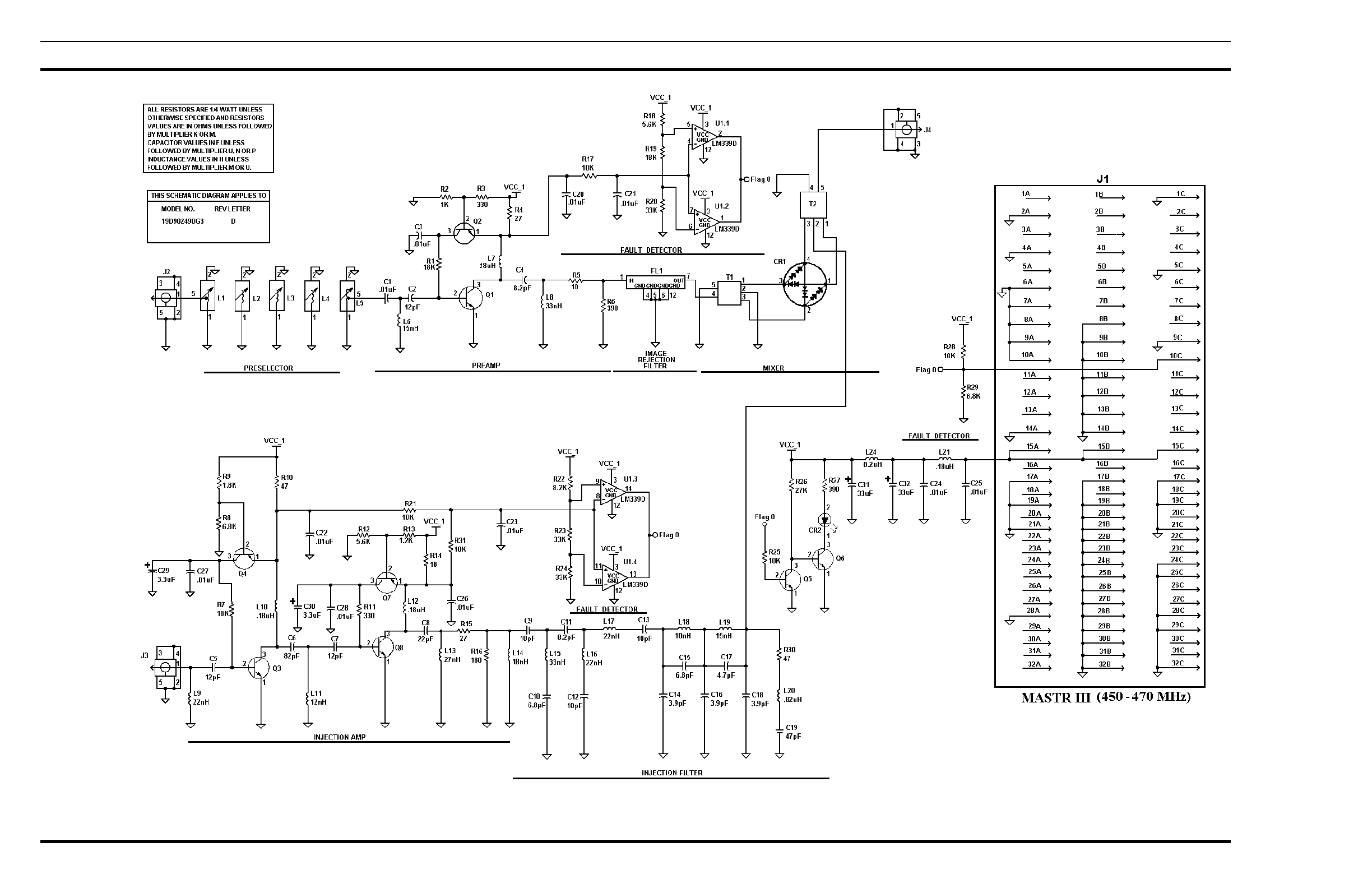
SCHEMATIC DIAGRAM
RECEIVER FRONT END MODULE
19D902782G3
(19D903498, Rev. 7)
LBI-38673F
10

This page intentionally left blank
LBI-38673F
11

LBI-38674F
TABLE OF CONTENTS
DESCRIPTION . . . . . . . . . . . . . . . . . . . . . . . . . . . . . . . . . . . . . . . . . . . . . . . 1
SPECIFICATIONS . . . . . . . . . . . . . . . . . . . . . . . . . . . . . . . . . . . . . . . . . . . . . 1
CIRCUIT ANALYSIS . . . . . . . . . . . . . . . . . . . . . . . . . . . . . . . . . . . . . . . . . . . . 1
POWER AMPLIFIER . . . . . . . . . . . . . . . . . . . . . . . . . . . . . . . . . . . . . . . . . 1
Exciter . . . . . . . . . . . . . . . . . . . . . . . . . . . . . . . . . . . . . . . . . . . . . . . 1
Small Signal Gain Stage . . . . . . . . . . . . . . . . . . . . . . . . . . . . . . . . . . . . . . 1
Low Level Amplifier . . . . . . . . . . . . . . . . . . . . . . . . . . . . . . . . . . . . . . . . 1
Driver . . . . . . . . . . . . . . . . . . . . . . . . . . . . . . . . . . . . . . . . . . . . . . . . 1
Power Amplifier Finals . . . . . . . . . . . . . . . . . . . . . . . . . . . . . . . . . . . . . . 1
POWER CONTROL . . . . . . . . . . . . . . . . . . . . . . . . . . . . . . . . . . . . . . . . . . . . . 2
Theory of Operation . . . . . . . . . . . . . . . . . . . . . . . . . . . . . . . . . . . . . . . . 2
Signal Interface . . . . . . . . . . . . . . . . . . . . . . . . . . . . . . . . . . . . . . . . . . . 2
TROUBLESHOOTING GUIDE . . . . . . . . . . . . . . . . . . . . . . . . . . . . . . . . . . . . . . 2,3
BLOCK DIAGRAM . . . . . . . . . . . . . . . . . . . . . . . . . . . . . . . . . . . . . . . . . . . . . 1
POWER AMPLIFIER READINGS . . . . . . . . . . . . . . . . . . . . . . . . . . . . . . . . . . . . . 3
ASSEMBLY DIAGRAM . . . . . . . . . . . . . . . . . . . . . . . . . . . . . . . . . . . . . . . . . . 5,6,7
PARTS LIST . . . . . . . . . . . . . . . . . . . . . . . . . . . . . . . . . . . . . . . . . . . . . . . . . 8
PRODUCTION CHANGES . . . . . . . . . . . . . . . . . . . . . . . . . . . . . . . . . . . . . . . . . 9,10
IC DATA . . . . . . . . . . . . . . . . . . . . . . . . . . . . . . . . . . . . . . . . . . . . . . . . . . . 11
OUTLINE DIAGRAM . . . . . . . . . . . . . . . . . . . . . . . . . . . . . . . . . . . . . . . . . . . 10,12
SCHEMATIC DIAGRAM . . . . . . . . . . . . . . . . . . . . . . . . . . . . . . . . . . . . . . . . . . 11,12
LOW PASS FILTER . . . . . . . . . . . . . . . . . . . . . . . . . . . . . . . . . . . . . . . . . . . . . 7,13
MAINTENANCE MANUAL FOR
450-470 MHz, 110 WATT POWER AMPLIFIER
19D902797G3
425-450 MHz, 90 WATT POWER AMPLIFIER
19D902797G7
403-425 MHz, 90 WATT POWER AMPLIFIER
19D902797G6
380-400 MHz, 75 WATT POWER AMPLIFIER
19D902797G8
470-494 MHz, 90 WATT POWER AMPLIFIER
19D902797G9
492-512 MHz, 90 WATT POWER AMPLIFIER
19D902797G10
410-430 MHz, 90 WATT POWER AMPLIFIER
19D902797G11
ericssonz
Ericsson Inc.
Private Radio Systems
Mountain View Road
Lynchburg, Virginia 24502
1-800-528-7711 (Outside USA, 804-592-7711) Printed in U.S.A.
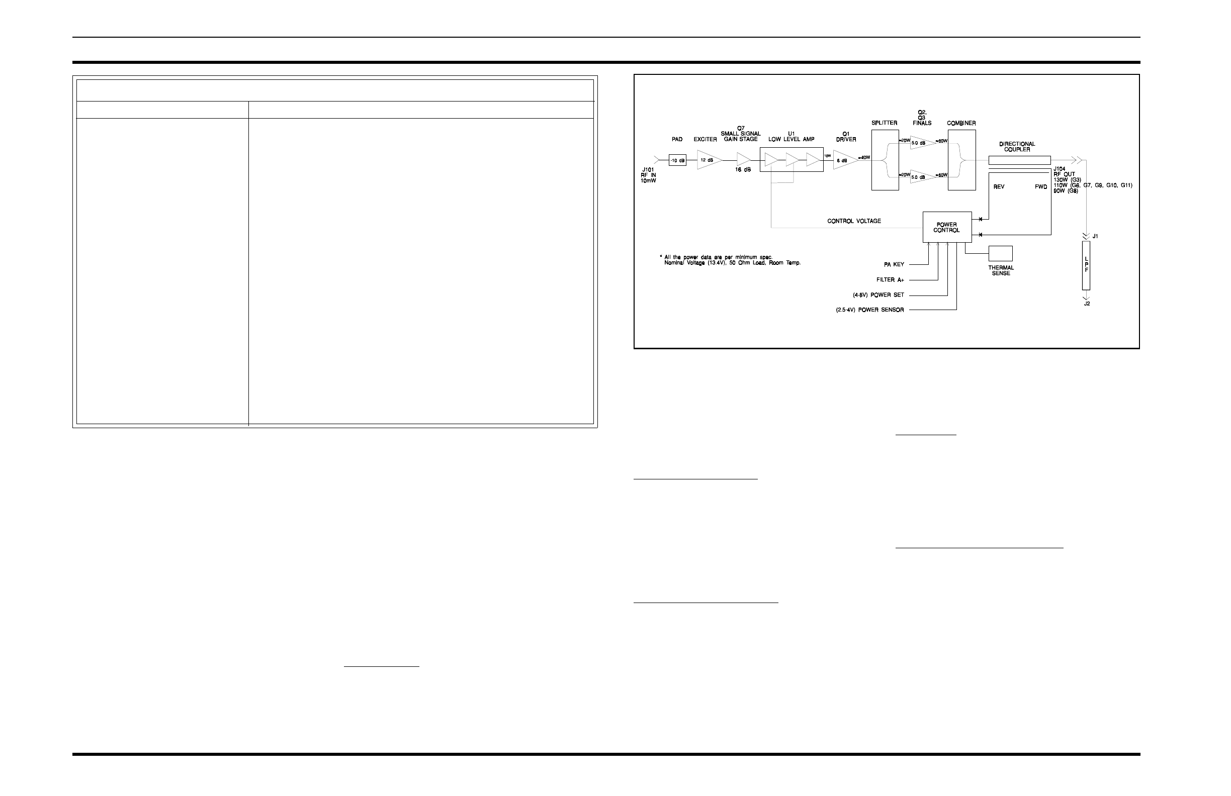
DESCRIPTION
The UHF Power Amplifier Assembly is a wide band RF
power amplifier operating over the 380-400, 410-430, 403-
425, 425-450, 450-470, 470-494, and 492-512 MHz range
without tuning. Its main function is to amplify the 10 mW FM
signal from the Transmitter Synthesizer to the rated RF output
at the antenna port. The output of the Power Amplifier Assem-
bly is adjustable from rated power to 3dB lower at the PA
output J104.
The assembly consists of a printed wiring board (A1) and
associated components, including a power module and three
RF power transistors, mounted to the heat sink assembly. The
printed wiring board (A1) contains both the power amplifier
circuitry and the power control circuitry.
Unfiltered supply voltage, A+, for the power amplifier
circuits enters the assembly via feedthrough capacitor, C1.
Power cable W4 routes the A+ from C1 to J103 on the PWB.
Filtered A+ voltage for the power control circuit enters the
assembly via control cable W13 which connects to the PWB at
J201.
The Power Control circuitry sets the output power level by
adjusting the PA Power Set level. It keeps the output power
constant despite variations in input power, power amplifier
gain, or temperature through the use of a feedback control loop
in the PA assembly.
CIRCUIT ANALYSIS
POWER AMPLIFIER
The power amplifier section of the PA Board consists of
an Exciter, a Small Signal Gain Stage, a Low Level Amplifier,
a Driver, and the Power Amplifier Finals. All these gain stages
have an input and output impedance of 50 ohms. Figure 1 is a
block diagram showing the signal flow within the Power Am-
plifier Assembly.
Exciter (U101)
The Exciter stage uses a broadband silicon monolithic
microwave integrated circuit (MMIC) amplifier. The signal
from transmitter synthesizer, typically 10 dBm (10 mW), is
input to the Exciter through a 10 dB resistive pad (R1, R2, and
R31). The Exciter amplifies the resulting 0 dBm (1 mW)
signal to 12 dBm (16 mW).
The MMIC requires a 5 volt supply source. The 8 volt
regulator (U100) provides the 5 volts to the MMIC via a
dropping resistor R30.
Small Signal Gain Stage
The Small Signal Gain Stage consists of Q7 and its
associated bias and matching circuitry. Collector voltage is
fed through R39, R40, and L23. Resistor R33 sets the quies-
cent bias of the part. The transistor input impedance is
matched to the 50 ohm output of the Exciter by C59, C61,
C62, and C63. L24 provides the necessary output matching.
The stage provides 14 dB of gain to amplify the signal from
the Exciter to 26 dBm (400 mW).
Low Level Amplifier (U102)
The Low Level Amplifier (LLA) stage uses a 50 ohm
thick film RF Power Module to amplify and control of the
output power. Internally, the module is a three stage ampli-
fier. The power control circuitry controls the gain of the first
and second stages by varying the collector voltage level of
Q203. The third stage gain remains constant with A+ provid-
ing the DC supply voltage.
The signal from the Small Signal Gain stage, typically
26 dBm (400 mW), is input into the LLA. Under typical
Power Set conditions, the LLA amplifies the signal to a
typical output level of 40.5 dBm (11.2 W).
Driver (Q1)
The driver is a 6 dB RF amplifier consisting of transistor
Q1 and its associated circuitry. The signal from the LLA,
typically 40.5 dBm (11.2 W), is amplified to 46.5 dBm (45.0
W). The transistor input is matched to 50 ohms by C65, C66,
C27, C67, and a piece of printed transmission line. The drive
signal is then split with a printed in-phase Wilkenson splitter,
providing equal power to each of the final devices.
Power Amplifier Finals (Q2, Q3)
Each of the Power Amplifier Final devices is capable of
producing 5 to 6 dB of gain. The output signal from the
Splitter is impedance matched to each of the finals. Under
optimum conditions each final amplifies the input signal to
between 50 and 70 watts output power (depending on band
split). The outputs are then impedance matched to the input
of the Combiner. The Combiner is a printed in-phase Wilkin-
son type which combines (sums) the output power of the
finals. This produces an output power of approximately
100W, (depending on band split) which is coupled to the
directional coupler (part of A1 PWB) and on to the antenna
circuits. In addition, the directional coupler samples both
forward and reverse power and sends this sample to the
Power Control circuitry.
Copyright © July 1992, Ericsson GE Mobile Communications Inc.
Table 1 - General Specifications
ITEM SPECIFICATION
FREQUENCY 450 MHz - 470 MHz (G3)
403 MHz - 425 MHz (G6)
425 MHz - 450 MHz (G7)
380 MHz - 400 MHz (G8)
470 MHz - 494 MHz (G9)
492 MHz - 512 MHz (G10)
410 MHz - 430 MHz (G11)
OUTPUT POWER (RF) 65 watts - 130 watts (G3)
55 watts - 110 watts (G6, G7, G9, G10 & G11)
45 watts - 90 watts (G8)
INPUT POWER (RF) 10 mW min. into ≤ 2:1 VSWR.
TEMPERATURE RANGE -30°C TO +60°C (Ambient air)
SUPPLY VOLTAGE 13.4 Vdc
CURRENT 29 Amps max. (26 A typical @ rated power, 13.4V) (G3)
29 Amps max. (21 A typical @rated power , 13.4V)(G6, G7, G9, G10 & G11)
29 Amps max. (20 A typical @ rated power, 13.4V) (G8)
DUTY CYCLE Continuous
STABILITY Stable into 3:1 VSWR; all temp.,voltage,freq. 55 watts - 110 watts (G3)
or 45 watts - 90 watts (G6, G7, G9, G10 & G11) or 45watts - 90 watts (G8)
RUGGEDNESS AT HIGH VSWR No damage into open or shorted load.
Figure 1 - Block Diagram
LBI-38674F
1

POWER CONTROL
The Power Control circuitry performs three basic func-
tions. It keys and unkeys the PA, sets the PA output power,
and protects the PA against adverse conditions.
Keying and Unkeying the PA
To key the PA, the digital controller places 5 volts on the
PA key line, J201-2. Zero volts on the PA key line causes the
PA to unkey. If the control cable (W13) is disconnected, with
nothing actively driving the PA key line, the PA will remain
unkeyed.
PA Output Power Set
PA output power is set according to the level of the
Power Set line. Four (4) volts on this line will produce
minimum power. As the voltage increases toward eight (8)
volts, the power will increase to its maximum rated output.
The PA output power is initially set at the factory. This is
done by adjusting R43 while injecting a 10 mW signal at J1
and applying 8 volts to J201-3. After setting the maximum
power level, changing the output power in done by varying
the voltage applied on the Power Set line.
PA Protection
The power control also protects the PA against over
temperature and high VSWR conditions.
An over temperature condition exists when the flange
temperature of the final output transistor reaches 80°C. At
this point the output power will drop below its set level. The
output power will continue to drop such that when the flange
temperature reaches 125°C the PA output drops at least 10
dB below its set level.
Reflected power is limited to 25% of the set power. If
the output VSWR degrades to worse than 3:1 the forward
power will be reduced to limit the reflected power to 25% of
the set power. The Power Sensor line indicates when the PA
is operating in a cutback condition. If the PA is keyed and
the power control is cutting back, the Power Sensor line will
drop to zero (0) volts and the PA alarm light on the station
will turn on.
Theory of Operation
Power control of the MASTR III Power Amplifier is
accomplished with a feedback control loop. The three possi-
ble feedback signals are: representation of forward power,
temperature sensitive scaled representation of forward
power, or representation of reflected power. These three
signals are input to a diode summing junction which selects
the largest of the three for use as the feedback.
The stripline directional coupler samples the output
power and produces a voltage, Vf, proportional to the for-
ward output power. The power control compares the forward
voltage, Vf, to a reference voltage at U3. The output of U3
controls the current flow thru Q5 and the output of Q203.
The collector output of Q203 adjusts the control voltage,
Vct1 and Vct2. This control voltage is capable of adjusting
the total PA output power since it provides the first two stages
DC supply to the Low Level Amplifier, U1.
During over temperature operation, a scaled repre-
sentation of the forward power is maintained constant by
varying the control voltage line. Thermal resistor RT1 sens-
ing an increase in temperature causes the output of U3.1 to
increase. If the output of U3.1 becomes larger than the other
feedback lines, the output of U3.4 will begin to decrease.
This in turn will cause the output of Q203 to decrease
reducing the supply voltage to U1. Since the scaling is a
function of temperature the power is reduced as the tempera-
ture increases.
Under VSWR cutback operation the reverse voltage, Vr,
representative of the reflected output power is held below a
threshold by reducing the control voltage as necessary. If Vr
increases at U3.1 beyond the preset threshold an increase at
U3.4 will result. This causes a subsequent reduction in the
control voltage to U1. Thus the power control circuit reduces
the output power in order to limit the reflected power to 25%
of the set power.
Signal Interface
The signal interface to the MASTR III Power Amplifier
is supported by a six position feedthrough connector, J201,
with the following pinout:
1–PWR Sensor
2–PA Key
3–PA PWR Set
4–NC
5–Ground
6–Fil A+
Pwr Sensor
This line indicates when the PA is experiencing adverse
conditions. Under normal operation, while the PA is keyed,
this line will be proportional to forward power. Minimum
power (zero watts) corresponds to 2.5 volts while maximum
power corresponds to 4.5 volts. This voltage is not tempera-
ture compensated and no effort is made to calibrate this
signal to an absolute power level. It is intended to provide a
relative indication of forward power and to discriminate
between normal and cutback operation.
Zero volts on this line, when the PA is keyed, indicates the
forward power is cutback. This power cutback may be due to
high reflected power or may be due to high PA temperatures.
This fault condition may indicate a problem with the PA or may
indicate a system problem external to the Power Amplifier.
High VSWR may be due to a poor antenna and high tempera-
ture may be due to a blocked cabinet vent. Zero volts on this
line, when the PA is keyed, does not indicate zero forward
power. Zero volts indicates the PA is protecting itself due to
adverse conditions. If the adverse condition, either high VSWR
or high temperature is eliminated, the power will return to
normal and the PWR SENSOR voltage will rise above 2.5
volts.
PA Key (Interface Connector pin 2)
This line is used to key and unkey the PA. UNKEY = 0
volt and KEY = 5 volts. The driver of this line must be capable
of supplying 5 volts at 1.0 mA. The appropriate key sequence
requires RF from the transmit synthesizer be input to the PA
before the KEY line is energized.
PA PWR Set (Interface Connector pin 3)
This line is used to set the RF Power Output of the PA.
Minimum power output equals 4 volts and maximum power
output equals 8 volts. The driver of this line must be capable
of supplying 8 volts at 1.0 mA.
Fil A+ (Interface Connector pin 6)
This line provides the filtered supply voltage for the Power
Control. The driver of this line must be capable of supplying
13.4 volts ±20% at 100 mA.
SYMPTOM AREAS TO CHECK INDICATIONS
1. No Power or low Power at 1. Measure the transmitter output The presence of power at this port
Antenna Port. power before the duplexer or is an indication of a defective
antenna switch (for simplex mode). duplexer, switch, or cables.
2. Measure the transmitter output The presence of power at this port
power before the low pass filter. is an indication of a defective filter
or cables.
3. Measure the transmitter output The presene of power at this port
power before the optional isolator is an indication of a defective isolator
at the PA output port. or cables.
2. No power at PA output port 1. Station is in receive mode.
and PA ALARM is OFF.
3. No power at PA output port 1. No RF input to PA. Check TX Synthesizer should deliver
and PA ALARM is ON. connection between PA and TX a minimum of 10 mW
Synthesizer. (10 dBm) to the PA.
2. Check the logic or DC inputs to
the PA from the Interface Board
through J201.
a. J201-2 PA KEY 5volts during transmit
b. J201-3 POWER SET 4 volts to 8 volts (4 volts
represents zero RF power)
c. J201-6 13.8 VF 13.8 Vdc ±20%
3. Defective PA Replace PA
TROUBLESHOOTING GUIDE
LBI-38674F
2
SYMPTOM AREAS TO CHECK INDICATIONS
4. Low power at PA output port 1. Low RF input to PA from TX Power should be a minimum of 10
and PA ALRAM is OFF. Synthesizer. mW (10 dBm).
2. Check the voltage on J201-3 For minimal output power, this
(POWER SET). voltage should be above 7 volts.
3. Check the power supply voltage Voltage should be minimal 13.4
on the collector of Q1, Q2 Vdc.
and Q3
4. One of the two final PA Replace the defective transistor.
transistors (Q2 or Q3) is
defective.
5. Low power at PA output port 1. Check for over temperature and/ The power control circuit protects
and PA ALARM is ON. or a high VSWR condition due to the PA by cutting back the power.
a mismatch at the output port. In case of a mismatch, refer to
symptom 1.
TROUBLESHOOTING GUIDE (cont’d)
PARAMETER REFERENCE READINGS
(50 ohm, -30°C to +60°C) SYMBOL (volts DC)
SUPPLY VOLTAGE A+ 13.4 V ±20%
CONTROL VOLTAGE Vct1 0 - 12 V
FORWARD VOLTAGE Vf 3 - 7 V
REVERSE VOLTAGE Vr 2 - 6 V
POWER SENSE J201-1 2.5 - 4 V
PA KEY J201-2 5 V
POWER SET J201-3 4 - 8 V
13.8 VF J201-6 13.8 V ±20%
UHF POWER AMPLIFIER VOLTAGE CHART
Group Low Mid High
Frequency G3
G6
G7
G8
G9
G10
G11
450 MHZ
403 MHZ
425 MHZ
380 MHZ
470 MHZ
492 MHZ
410 MHZ
460 MHZ
414 MHZ
437 MHZ
390 MHZ
482 MHZ
502 MHZ
420 MHZ
470 MHZ
425 MHZ
450 MHZ
400 MHZ
494 MHZ
512 MHZ
430 MHZ
Vct 1 (Volts DC) G3
G6
G7
G8
G9 & G10
G11
7 - 10 Volts
6 - 8 Volts
6 - 8 Volts
6 - 8 Volts
6 - 8 Volts
6 - 8 Volts
6 - 8 Volts
6 - 8 Volts
6 - 8 Volts
6 - 8 Volts
6 - 8 Volts
6 - 8 Volts
4 - 6 Volts
6 - 8 Volts
6 - 8 Volts
6 - 8 Volts
6 - 8 Volts
6 - 8 Volts
Vf (Volts DC) G3
G6
G7
G8
G9 & G10
G11
5 - 7 Volts
6 - 8 Volts
6 - 8 Volts
6 - 8 Volts
6 - 8 Volts
6 - 8 Volts
5 - 7 Volts
6 - 8 Volts
6 - 8 Volts
6 - 8 Volts
6 - 8 Volts
6 - 8 Volts
5 - 7 Volts
6 - 8 Volts
6 - 8 Volts
6 - 8 Volts
6 - 8 Volts
6 - 8 Volts
Vr (Volts DC) G3
G6
G7
G8
G9 & G10
G11
2 - 3 Volts
2 - 3 Volts
2 - 3 Volts
2 - 3 Volts
2 - 3 Volts
2 - 3 Volts
2 - 3 Volts
2 - 3 Volts
2 - 3 Volts
2 - 3 Volts
2 - 3 Volts
2 - 3 Volts
2 - 3 Volts
2 - 3 Volts
2 - 3 Volts
2 - 3 Volts
2 - 3 Volts
2 - 3 Volts
J201 - 1 (Volts DC) G3
G6
G7
G8
G9 & G10
G11
2.5 - 4 Volts
2.5 - 4 Volts
2.5 - 4 Volts
2.5 - 4 Volts
2.5 - 4 Volts
2.5 - 4 Volts
2.5 - 4 Volts
2.5 - 4 Volts
2.5 - 4 Volts
2.5 - 4 Volts
2.5 - 4 Volts
2.5 - 4 Volts
2.5 - 4 Volts
2.5 - 4 Volts
2.5 - 4 Volts
2.5 - 4 Volts
2.5 - 4 Volts
2.5 - 4 Volts
J201 - 3 (Volts DC) G3
G6
G7
G8
G9 & G10
G11
6 - 8 Volts
6 - 8 Volts
6 - 8 Volts
6 - 8 Volts
6 - 8 Volts
6 - 8 Volts
6 - 8 Volts
6 - 8 Volts
6 - 8 Volts
6 - 8 Volts
6 - 8 Volts
6 - 8 Volts
6 - 8 Volts
6 - 8 Volts
6 - 8 Volts
6 - 8 Volts
6 - 8 Volts
6 - 8 Volts
J201- 6 (Volts DC) G3
G6
G7
G8
G9 & G10
G11
13.4 Volts
13.4 Volts
13.4 Volts
13.4 Volts
13.4 Volts
13.4 Volts
13.4 Volts
13.4 Volts
13.4 Volts
13.4 Volts
13.4 Volts
13.4 Volts
13.4 Volts
13.4 Volts
13.4 Volts
13.4 Volts
13.4 Volts
13.4 Volts
UHF POWER AMPLIFIER TYPICAL VOLTAGE READINGS
(50 ohm, room temperature, 13.4 Vdc supply voltage, and rated output)
LBI-38674F
3

FREQUENCY STANDARD ADJUSTABLE WITH WITH WITH DUPLEXER
MHz @J2 RANGE DUPLEXER ISOLATOR AND ISOLATOR
@J104
450-470 110W 65-130W 75W 100W 70W
425-450 90W 55-110W 60W 82W 55W
403-425 90W 55-110W 60W 82W 55W
380-400 75W 45-90W 50W 68W 47W
410-430 90W 55-110W 60W 82W 55W
470-494 90W 55-110W 60W 82W 55W
492-512 90W 55-110W 60W 82W 55W
RATED POWER FOR MASTR III UHF BASE STATION
LBI-38674F
4
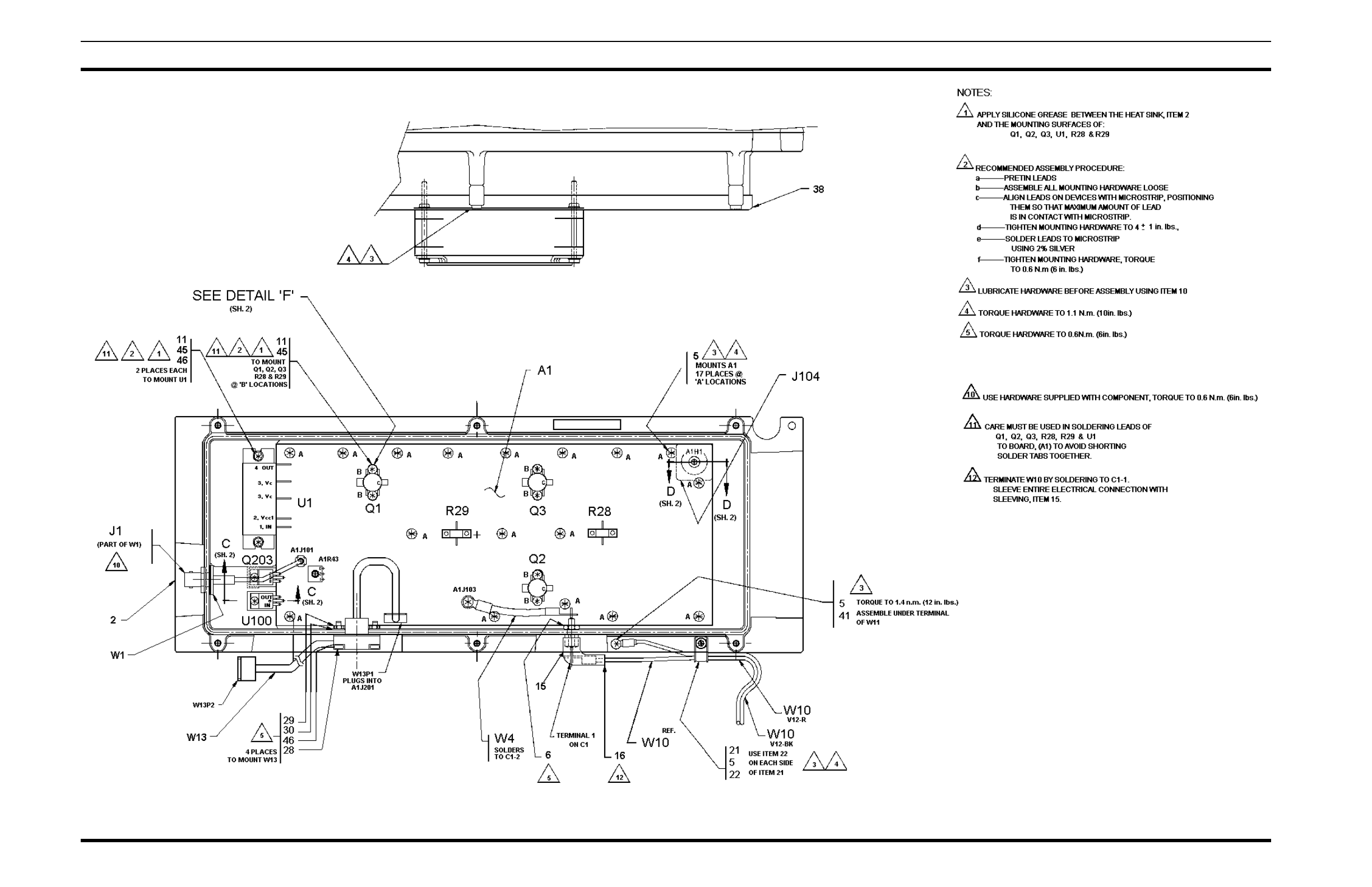
ASSEMBLY DIAGRAM
POWER AMPLIFIER ASSEMBLY
19D902797G3, G6, G7, G8, G9, G10 & G11
(19D902797 Sh. 3, Rev. 10)
LBI-38674F
5
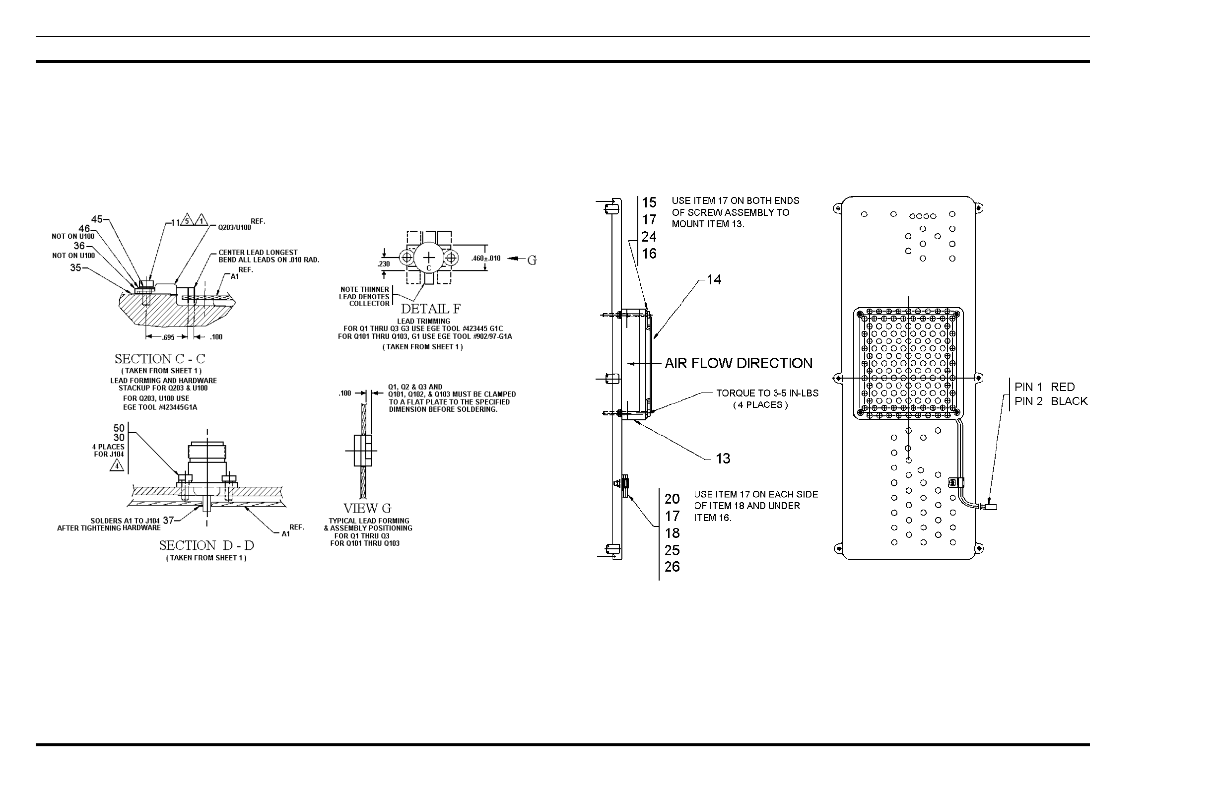
ASSEMBLY DIAGRAM
POWER AMPLIFIER ASSEMBLY
19D902797G3, G6, G7, G8, G9, G10 & G11
(19D902797 Sh. 2, Rev. 10)
COVER ASSEMBLY
19B801659G3
(19B801659, Sh. 2, Rev. 3)
LBI-38674F
6

ASSEMBLY DIAGRAMS
LOW PASS FILTER MODULE
19D902856G3
(19D902856 Sh. 1, Rev. 0)
LBI-38674F
7
110 WATT UHF POWER AMPLIFIER 19D902797G3
90 WATT UHF POWER AMPLFIER 19D902797G6, G7
& G9 - G11
75 WATT UHF POWER AMPLFIER 19D902797G8
ISSUE 6
PARTS LIST
SYMBOL PART NO. DESCRIPTION
ASSEMBLIES
A1 POWER AMPLIFIER BOARD
19D902794G3, G6 - G11
- - - - - - - - - - CAPACITORS - - - - - - - - - - -
C1 19A116708P2 Feedthru: 0.01uF +100-0%, 500 VDCW; sim to Erie 327-
050-X5W0103P.
C1 19A702052P26 Ceramic: 0.1 µF ±10%, 50 VDCW,
C2
thru
C9
19A702061P63 Ceramic: 120 pF ±5%, 50 VDCW, temp coef 0 ±30 PPM.
C10 344A3126P38 Porcelain: 100 pF ±5%, 500 VDCW. sim to 101JT500X.
C11 19A702061P63 Ceramic: 120 pF ±5%, 50 VDCW, temp coef 0 ±30 PPM.
C12 19A705108P40 Mica chip: 120 pF, ±5%, 100 VDCW. temp coef 0 ±50
PPM°C.
C13
thru
C16
344A3126P38 Porcelain: 100 pF ±5%, 500 VDCW. sim to 101JT500X.
C17 19A702052P26 Ceramic: 0.1 µF ±10%, 50 VDCW.
C18 19A705108P40 Mica chip: 120 pF, ±5%, 100 VDCW. temp coef 0 ±50
PPM°C.
C19 344A3126P38 Porcelain: 100 pF ±5%, 500 VDCW. sim to 101JT500X.
C20
and
C21
19A705108P40 Mica chip: 120 pF, ±5%, 100 VDCW. temp coef 0 ±50
PPM°C.
C22
and
C23
19A702052P26 Ceramic: 0.1 µF ±10%, 50 VDCW.
C24 19A702061P63 Ceramic: 120 pF ±5%, 50 VDCW, temp coef 0 ±30 PPM.
C25 344A3126P38 Porcelain: 100 pF ±5%, 500 VDCW. sim to 101JT500X.
C26 344A3126P62 Porcelain: 1000 pF ±5%, 500 VDCW; sim to 102JT500X.
C27 344A3126P13 Porcelain: 15 pF ±5%, 500 VDCW; sim to 100JT500X.
(Used in G7 and G8).
C27 344A3126P15 Porcelain: 12 pF ±5%, 500 VDCW; sim to 120JT500X.
(Used in G6 and G11).
C28 344A3126P18 Porcelain: 15 pF ±5%, 500 VDCW; sim to 150JT500X.
(Used in G8).
C28 344A3126P15 Porcelain: 12 pF ±5%, 500 VDCW; sim to 120JT500X.
(Used in G6).
C28 344A3126P13 Porcelain: 15 pF ±5%, 500 VDCW; sim to 100JT500X.
(Used in G11).
C28 344A3126P11 Porcelain: 8.2 pF ±5%, 500 VDCW; sim to 8R2CT500X.
(Used in G7).
C29 344A3126P18 Porcelain: 15 pF ±5%, 500 VDCW; sim to 150JT500X.
(Used in G8).
C29 344A3126P15 Porcelain: 12 pF ±5%, 500 VDCW; sim to 120JT500X.
(Used in G6).
C29 344A3126P13 Porcelain: 15 pF ±5%, 500 VDCW; sim to 100JT500X.
(Used in G11).
C29 344A3126P11 Porcelain: 8.2 pF ±5%, 500 VDCW; sim to 8R2CT500X.
(Used in G7).
C30 344A3126P15 Porcelain: 12 pF ±5%, 500 VDCW; sim to 120JT500X.
(Used in G8).
C30 344A3126P11 Porcelain: 8.2 pF ±5%, 500 VDCW; sim to 8R2CT500X.
(Used in G3, G9, G10).
C31 344A3126P15 Porcelain: 12 pF ±5%, 500 VDCW; sim to 120JT500X.
(Used in G8).
C31 344A3126P11 Porcelain: 8.2 pF ±5%, 500 VDCW; sim to 8R2CT500X.
(Used in G3, G9, G10).
C32
and
C33
344A3126P1 Porcelain: 3.3 pF ±.25pF, 500 VDCW; sim to 3R3CT500X.
(Used in G3).
SYMBOL PART NO. DESCRIPTION
C34
and
C35
344A3126P18 Porcelain: 15 pF ±5pF, 500 VDCW; simto 150JT500X.
(Used in G6, G7 and G11).
C36 344A3126P3 Porcelain: 3.9 pF ±0.25%, 500 VDCW; sim to
3R9CT500X. (Used in G8).
C36 344A3126P5 Porcelain: 4.7 pF ±0.25%, 500 VDCW; sim to
4R7CT500X. (Used in G6 and G11).
C37 344A3126P2 Porcelain: 2.2 pF ±0.25%, 500 VDCW; sim to
2R2CT500X. (Used in G8).
C38 19A705205P7 Tantalum: 10 µF, 25 VDCW; sim to Sprague 293D. (Used
in G8, G9, G10 and G11).
C39 19A705108P40 Mica chip: 120 pF, ±5%, 100 VDCW. temp coef 0 ±50
PPM/°C. (Used in G8, G9, G10 and G11).
C40 19A702052P26 Ceramic: 0.1 µF ±10%, 50 VDCW. (Used in G8, G9 and
G10).
C41 344A3126P38 Porcelain: 100 pF ±5%, 500 VDCW. sim to 101JT500X.
(Used in G11).
C42
thru
C45
19A702052P26 Ceramic: 0.1 µF ±10%, 50 VDCW.
C46
and
C47
344A3126P11 Porcelain: 8.2 pF ±5%, 500 VDCW; sim to 8R2CT500X.
(Used in G9 and G10).
C46
and
C47
344A3126P13 Porcelain: 15 pF ±5%, 500 VDCW; sim to 100JT500X.
(Used in G10).
C48 19A702052P26 Ceramic: 0.1 µF ±10%, 50 VDCW.
C49 19A702236P40 Ceramic: 39 pF ±5%, 50 VDCW, temp coef 0 ±30 PPM/°C.
C50 19A702052P26 Ceramic: 0.1 µF ±10%, 50 VDCW.
C51 19A705205P7 Tantalum: 10 µF, 25 VDCW; sim to Sprague 293D.
C53
and
C54
19A705205P7 Tantalum: 10 µF, 25 VDCW; sim to Sprague 293D.
C57 19A705205P7 Tantalum: 10 µF, 25 VDCW; sim to Sprague 293D.
C58 344A3126P11 Porcelain: 8.2 pF ±5%, 500 VDCW; sim to 8R2CT500X.
(Used in G3).
C58 344A3126P15 Porcelain: 12 pF ±5%, 500 VDCW ; sim to 120JT500X.
(Used in G6, G7, G8 and G11).
C58 344A3126P7 Porcelain: 5.6 pF ±0.25%, 500 VDCW; sim to
5R6CT500X. (Used in G9, G10).
C59 19A702061P49 Ceramic: 56 pF ±5%, 50 VDCW, temp coef 0 ±30 PPM.
C60 19A702061P65 Ceramic: 150 pF ±5%, 50 VDCW, temp coef 0 ±30
PPM/°C.
C61 19A702061P17 Ceramic: 12 pF ±10 pF, 50 VDCW, temp coef 0 ±30
PPM/°C.
C62 19A702236P52 Ceramic: 120 pF ±5%, 50 VDCW, temp coef 0 ±30
PPM/°C.
C64 344A3126P38 Porcelain: 100 pF ±5%, 500 VDCW; sim to 101JT500X.
C65 344A3126P11 Porcelain: 8.2 pF ±5%, 500 VDCW; sim to 8R2CT500X.
(Used in G3).
C65 344A3126P5 Porcelain:4.7 pF ±0.25%, 500 VDCW; sim to 4R7CT500X.
(Used in G9, G10).
C66 19A700006P58 Mica/teflon: 47 pF ±2%, 100 VDCW. (Used in G8).
C66 19A700006P55 Mica/teflon: 27 pF ±2%, 100 VDCW. (Used in G9 and
G10).
C66 19A700006P50 Mica/teflon: 39 pF ±2%, 100 VDCW. (Used in G6, G7, and
G11).
C66 19A700006P48 Mica/teflon: 33 pF ±2%, 100 VDCW. (Used in G3).
C67 19A700006P58 Mica/teflon: 47 pF ±2%, 100 VDCW. (Used in G6 and
G11).
C67 19A700006P50 Mica/teflon: 39 pF ±2%, 100 VDCW. (Used in G7 and G8).
C67 19A700006P49 Mica/teflon: 36 pF ±2%, 100 VDCW (G3).
C67 19A700006P55 Mica/teflon: 27 pF ±2%, 100 VDCW. (Used in G9 and
G10).
C68 19A700006P58 Mica/teflon: 47 pF ±2%, 100 VDCW. (Used in G8 and
G11).
C68 19A700006P50 Mica/teflon: 39 pF ±2%, 100 VDCW. (Used in G6, G7, and
G11).
C68 19A700006P48 Mica/teflon: 33 pF ±2%, 100 VDCW (G3).
SYMBOL PART NO. DESCRIPTION
C68
and
C69
19A700006P53 Mica/teflon: 22 pF ±2%, 100 VDCW. (Used in G10).
C68 19A700006P55 Mica/teflon: 27 pF ±2%, 100 VDCW. (Used in G9).
C69 19A700006P49 Mica/teflon: 36 pF ±2%, 100 VDCW (G3).
C69 19A700006P58 Mica/teflon: 47 pF ±2%, 100 VDCW. (Used in G6 and G11).
C69 19A700006P50 Mica/teflon: 39 pF ±2%, 100 VDCW (G7).
C69 19A700006P55 Mica/teflon: 27 pF ±2%, 100 VDCW. (Used in G9).
C69 19A700006P57 Mica/teflon: 43 pF ±2%, 100 VDCW. (Used in G8).
C70 19A702061P49 Ceramic: 56 pF ±5%, 50 VDCW, temp coef 0 ±30 PPM.
C71 19A702061P63 Ceramic: 120 pF ±5%, 50 VDCW, temp coef 0 ±30 PPM.
C72
and
C73
19A702052P26 Ceramic: 0.1 µF ±10%, 50 VDCW.
C75
thru
C77
19A702052P26 Ceramic: 0.1 µF ±10%, 50 VDCW.
C78
and
C79
19A705205P7 Tantalum: 10 µF, 25 VDCW; sim to Sprague 293D.
C81 344A3126P62 Porcelain: 1000 pF ±5%, 500 VDCW; sim to 102JT500X.
C82
and
C83
19A705108P40 Mica chip: 120 pF, ±5%, 100 VDCW, temp coef 0 ±50 PPM/°C.
C84 19A702061P89 Ceramic: 1500 pF ±5%, 50 VDCW, temp coef 0 ±30
PPM.(Used in G3, G6-G9, G11).
C85
and
C86
19A705108P40 Mica chip: 120 pF, ±5%, 100 VDCW, temp coef 0 ±50 PPM/°C.
C87 19A700006P60 Mica/teflon: 56 pF ±2%, 100 VDCW. (Used in G8).
C87 19A700006P58 Mica/teflon: 47 pF ±2%, 100 VDCW. (Used in G6, and G11).
C87 19A700006P57 Mica/teflon: 43 pF ±2%, 100 VDCW. (Used in G7).
C87 19A700006P50 Mica/teflon: 39 pF ±2%, 100 VDCW. (Used in G3).
C87 19A700006P48 Mica/teflon: 33 pF ±2%, 100 VDCW. (Used in G9 and G10).
C88 19A700006P59 Mica/teflon: 51 pF ±2%, 100 VDCW. (Used in G6, G8, and
G11).
C88 19A700006P57 Mica/teflon: 43 pF ±2%, 100 VDCW. (Used in G7).
C88 19A700006P50 Mica/teflon: 39 pF ±2%, 100 VDCW. (Used in G3).
C88 19A700006P48 Mica/teflon: 33 pF ±2%, 100 VDCW. (Used in G9 and G10).
C89 19A700006P59 Mica/teflon: 51 ohms ±2%, 100 VDCW. (Used in G6, G8, and
G11).
C89 19A700006P57 Mica/teflon: 43 pF ±2%, 100 VDCW. (Used in G7).
C89 19A700006P50 Mica/teflon: 39 pF ±2%, 100 VDCW. (Used in G3).
C89 19A700006P48 Mica/teflon: 33 pF ±2%, 100 VDCW. (Used in G9 and G10).
C90 19A700006P60 Mica/teflon: 56 pF ±2%, 100 VDCW. (Used in G8).
C90 19A700006P58 Mica/teflon: 47 pF ±2%, 100 VDCW. (Used in G6 and G11).
C90 19A700006P57 Mica/teflon: 43 pF ±2%, 100 VDCW. (Used in G7).
C90 19A700006P50 Mica/teflon: 39 pF ±2%, 100 VDCW. (Used in G3).
C90 19A700006P48 Mica/teflon: 33 pF ±2%, 100 VDCW. (Used in G9 and G10).
C91 19A700006P57 Mica/teflon: 43 pF ±2%, 100 VDCW. (Used in G8).
C91 19A700006P58 Mica/teflon: 47 pF ±2%, 100 VDCW. (Used in G9 and G11).
C91 19A700006P49 Mica/teflon: 36 pF ±2%, 100 VDCW. (Used in G7).
C91 19A700006P48 Mica/teflon: 33 pF ±2%, 100 VDCW. (Used in G3, G9 and
G10).
C92 19A700006P59 Mica/teflon:(Used in G8).
C92 19A700006P57 Mica/teflon: 43 pF ±2%, 100 VDCW. (Used in G6 and G11).
C92 19A700006P50 Mica/teflon: 39 pF ±2%, 100 VDCW. (Used in G7).
C92 19A700006P48 Mica/teflon: 33 pF ±2%, 100 VDCW. (Used in G3).
C92 19A700006P55 Mica/teflon: 27 pF ±2%, 100 VDCW. (Used in G9 and G10).
C93 19A700006P59 Mica/teflon: 51 ohms ±2%, 100 VDCW. (Used in G8).
C93 19A700006P57 Mica/teflon: 43 pF ±2%, 100 VDCW. (Used in G6 and G11).
C93 19A700006P50 Mica/teflon: 39 pF ±2%, 100 VDCW. (Used in G7).
SYMBOL PART NO. DESCRIPTION
C93 19A700006P48 Mica/teflon: 33 pF ±2%, 100 VDCW. (Used in G3).
C93 19A700006P55 Mica/teflon: 27 pF ±2%, 100 VDCW. (Used in G9 and G10).
C94 19A700006P57 Mica/teflon: 43 pF ±2%, 100 VDCW. (Used in G8).
C94 19A700006P49 Mica/teflon: 36 pF ±2%, 100 VDCW (G7).
C94 19A700006P58 Mica/teflon: 47 pF ±2%, 100 VDCW. (Used in G6 and G11).
C94 19A700006P48 Mica/teflon: 33 pF ±2%, 100 VDCW. (Used in G3, G9, and
G10).
- - - - - - - - - - - - DIODES - - - - - - - - - - - -
D1
thru
D3
19A705377P4 Silicon: Hot Carrier; sim to HP HSMS-2802.
D4
thru
D6
19A700053P3 Silicon: 2 Diodes in Series, Common Cathode; sim to
MBAV70L.
- - - - - - - - - - - - - - JACKS - - - - - - - - - - - - - -
J101 19A705512P1 Connector, RF SMB Series: sim to AMP No. 221111-1.
J103 19A134263P1 Contact, electrical: sim to Selectro 229-1082-00-0-590.
J104 7777145P5 Receptacle: sim to Amphenol 82-97.
J201 19A704852P32 Printed wire, two part: 6 contacts, sim
to Molex 22-29-2061.
- - - - - - - - - - - - - - INDUCTORS - - - - - - - - - - - - - -
L1 19C320617P10 Coil.(Used in G3, G6-G9 and G11).
L1 19C320617P17 Coil.(Used in G10).
L2 19A701091G1 Coil (Used in G6, G7, G8 and G11).
L3 19C320617P10 Coil (Used in G6, G7, G8, G10 and G11).
L4 19C320617P28 Coil.
L5 19A701091G1 Coil (Used in G6, G7, G8 and G11).
L6 19C320617P10 Coil (Used in G6, G7, G8, G10 and G11).
L7 19A705470P4 Coil, Fixed: 15 nH; sim to Toko 380NB-15nM.
L8 19A705470P8 Coil, Fixed: 39 nH; sim to Toko 380NB-39nM.
L14 19C320617P17 Coil.
L15
thru
L17
19A700024P13 Coil, RF: 1.0 µH ±20%.
L18 19C320617P17 Coil.
L23 19A705470P8 Coil, Fixed: 39 nH; sim to Toko 380NB-39nM.
L25 19A701091G1 Coil.
L29
and
L30
19C320617P10 Coil.
- - - - - - - - - - - TRANSISTORS - - - - - - - - - - - -
Q1 344A3948P1 Silicon, NPN: 440-512 MHz, 50W; sim to MRF 650.
Q2
and
Q3
344A4134P1 Silicon, NPN: 470-512 MHz, 65W; sim to MRF 658.
Q4
and
Q5
19A700076P2 Silicon, NPN: sim to MMBT3904, low profile.
Q7 19A701940P1 Silicon, NPN: sim to MRF 559.
Q7 344A3058P1 Silicon, NPN.
Q203 19A700055P1 Silicon, PNP.
- - - - - - - - - - - - RESISTORS - - - - - - - - - - - -
R1
and
R2
19B800607P270 Metal film: 27 ohms ±5%, 1/8 w.
R3
thru
R6
19B801486P101 Metal film: 100 ohms ±5%, 1/2 w.
R7 19B800607P183 Metal film: 18K ohms ±5%, 1/8 w.
* COMPONENTS, ADDED, DELETED OR CHANGED BY PRODUCTION CHANGES
LBI-38674F
8
PARTS LIST & PRODUCTION CHANGES
LOW PASS FILTER MODULE
19D902856G3 & G9
ISSUE 2
SYMBOL PART NO. DESCRIPTION
R8
thru
R10
19B800607P103 Metal film: 10K ohms ±5%, 1/8 w.
R11 19B800607P223 Metal film: 22K ohms ±5%, 1/8 w.
R12
thru
R18
19B800607P103 Metal film: 10K ohms ±5%, 1/8 w.
R19
and
R20
19B800607P472 Metal film: 4.7K ohms ±5%, 1/8 w.
R21
thru
R23
19B800607P102 Metal film: 1K ohms ±5%, 1/8 w.
R24
thru
R26
19B800607P103 Metal film: 10K ohms ±5%, 1/8 w.
R27 19B800607P822 Metal film: 8.2K ohms ±5%, 1/8 w.
R28
and
R29
19A143832P6 Power: 100 ohms ±5%, 40 w.
R30 19B800607P750 Metal film: 75 ohms ±5%, 1/8w.
R31 19B800607P330 Metal film: 33 ohms ±5%, 1/8 w.
R32 19A700050P17 Wirewound: 2.2 ohms ±10%, 2 w. (Used in G3, G9, and G10).
R33 19B800607P392 Metal film: 3.9K ohms ±5%, 1/8 w.
R34 19B801486P100 Metal film: 10 ohms ±5%, 1/2 w.
R35 19A700050P17 Wirewound: 2.2 ohms ±10%, 2 w. (Used in G3, G9).
R36 19B801486P101 Metal film: 100 ohms ±5%, 1/2 w. (Used in G40, G3, and G6).
R37 19B801486P331 Metal film: 330 ohms ±5%, 1/2 w. (Used in G3, G6-G9, G11).
R38 19B800607P223 Metal film: 22K ohms ±5%, 1/8 w.
R39
and
R40
19B800607P100 Metal film: 10 ohms ±5%, 1/8 w.
R41 19A702931P333 Metal film: 21.5K ohms ±1%, 200 VDCW, 1/8 w.
R42 19A702931P293 Metal film: 9090 ohms ±1%, 200 VDCW, 1/8 w.
R43 19A700109P5 Variable, cermet: 25 ohms to 10K ohms ±20%, 1/4 w.
R44
thru
R46
19B801486P101 Metal film: 100 ohms ±5%, 1/2 w.
R47
and
R48
19B801486P750 Metal film: 75 ohms ±5%, 1/2 w.
R49 19B801486P101 Metal film: 100 ohms ±5%, 1/2 w. (Used in G3, G6-G9, G11).
R50 19B800607P1 Metal film: Jumper. (Used in G8, G9, G10 and G11).
R51 19B801486P331 Metal film: 330 ohms ±5%, 1/2 w.(Used in G3, G6-G9, G11).
R52 19B801486P100 Metal film: 10 ohms ±5%, 1/2 w.
R53 19B800607P1 Metal film: Jumper.
R54 19B800607P472 Metal film: 4.7 ohms ±5%, 1/8 w.
R55 19B800607P103 Metal film: 10K ohms ±5%, 1/8 w.
R56 19B800607P330 Metal film: 33 ohms ±5%, 1/8 w.
R57 19B800607P222 Metal film: 2.2 ohms ±5%, 1/8 w.
R58
and
R59
19A700113P7 Composition: 4.7 ohms ±5%, 1/2 w (Used in G10).
- - - - - - - - - - - - - - THERMISTOR - - - - - - - - - - - - - -
RT1 19A705813P2 Thermistor: sim to AL03006-58.2K-97-G100.
- - - - - - - - - - - VOLTAGE REGULATORS - - - - - - - - - - -
VR1
and
VR2
19A700083P102 Silicon: 5.1 Volt Zener; sim to BZX84-C5V1.
- - - - - - - - - - - - - - CAPACITORS - - - - - - - - - - - - - -
C1 19A116708P2 Ceramic feedthru: 0.01 µF -0 +100%, 500 VDCW; sim to Erie
327-050-X5W0103P.
SYMBOL PART NO. DESCRIPTION
- - - - - - - - - - - - - - JACKS - - - - - - - - - - - - - -
J1 Part of W1.
J104 7777145P5 Receptacle: sim to Amphenol 82-97.
- - - - - - - - - - - - - - TRANSISTORS - - - - - - - - - - - - - -
Q1 344A3948P1 Silicon, NPN: UHF Amplifier; sim to Motorola MRF 650.
Q2
and
Q3
344A4134P1 Silicon, NPN: UHF Amplifier.
Q203 19A700055P1 Silicon, PNP: Darlington; sim to TIP-125.
- - - - - - - - - - - - - - RESISTORS - - - - - - - - - - - - - -
R28
and
R29
19A143832P6 Power: 100 ohm 5%, 40 w.
- - - - - - - - - - -INTEGRATED CIRCUITS - - - - - - - - - - - -
U1 19A705457P2 PA module: 440-470 MHz; sim to M57704H. (Used in G3).
U1 19A705457P1 PA module: 400-450 MHz; sim to M57704M. (Used in G7).
U1 19A705457P3 PA module: 470-512 MHz; sim to M57704SH. (Used in G9
and G10).
U1 19A705457P7 PA module: 380-400 MHz; sim to M57704UL. (Used in G8).
U1 19A705457P4 PA module: 400-420 MHz; sim to M57704L. (Used in G6).
U2 19A702293P3 Linear: Dual Op Amp; sim to LM358D.
U3 19A701789P4 Linear: Quad Op Amp; sim to LM224D.
U7 344A3907P1 Monolithic microwave IC (MMIC): sim to Avantek MSA-1105.
U100 19A705532P2 Integrated Circuit, Linear (Positive Voltage Regulator): sim to
MC78T15CT.
- - - - - - - - - - - - - - - - CABLES - - - - - - - - - - - - - - - -
W1 19B801529G4 RF Input Cable. Includes the following:
19B800560P2 RF Cable.
19A705512P3 Connector, RF SMB series: sim to AMP 228213-1.
19A115938P1 Connector, coaxial: (BNC Series); sim to Amphenol 31-318.
W4 19B801695G11 Power Cable. Includes the following:
19B209268P115 Solderless terminal.
19B209260P11 Solderless terminal.
19A115959P2 Wire, stranded.
19A701503P2 Cable: battery, red.
19A701503P10 Cable: battery, black.
19B209268P116 Solderless terminal.
W10 19B801937P1 Power cable.
W13 19B801739P1 Power control cable.
- - - - - - - - - - - - - MISCELLANEOUS - - - - - - - - - - - -
2 19D902420P6 Heatsink.
5 19A702381P510 Screw, thread forming: TORX DRIVE No. M3.5 0.6 x 10.
6 7139898P3 Nut, hex, brass: No. 1/4-28.
11 19A702364P310 Machine screw, TORX Drive: No. M3-0.5 x 10.
14 19B209268P113 Terminal, solderless: sim to AMP 2-34835-4. (Used in G11).
19A115959P2 Wire, stranded. (Used in G11).
19B209268P116 Solderless terminal. (Used in G11).
15 7147306P2 Insulator.
16 19A700136P7 Insulated sleeving.
21 19A701863P27 Clip, loop.
22 19A701312P5 Flatwasher: M3.5.
28 19A702364P316 Machine Screw: Pan Head, Steel.
29 19A700034P4 Nut, hex: No. M3 x 0.5MM.
30 19A700033P5 Lock washer, external tooth: No. 3.
SYMBOL PART NO. DESCRIPTION
35 19A705469P1 Insulator Plate, TO-220.
36 19A700068P1 Insulator, bushing.
37 19A134455P3 Flat washer.
38 19B801659G3 Cover (see separate parts list).
41 19A700033P6 Loackwasher, external tooth, M3.5.
45 N405P5B6 Lockwasher.
46 19A701312P4 Flatwasher: 3.2 ID.
50 19A702381P408 Tap screw, TORX Drive, M3-0.5 x 8.
51 19A705106P1 Resistor Spacer.
COVER
19B801659G3
2 19D902421P1 Power Amplifier Cover.
4 19A702381P522 Screw, thread forming:
5 19A701365P4 Washer.
11 19A149969P3 Shield.
13 5493477P9 Axial fan.
14 5493477P10 Grille.
15 N80P13028B6 Machine screw.
16 N210P21B6 Machine nut.
17 19A701312P5 Flatwasher: M3.5.
18 19A701863P10 Clip, loop.
20 19A702364P410 Machine screw.
24 N405P37B6 Lock washer.
25 L401P23B6 Split washer.
26 19A700034P5 Hex nut.
SYMBOL PART NO. DESCRIPTION
- - - - - - - - - - - - - JACKS - - - - - - - - - - - - -
J1
and
J2
7777145P5 Receptacle: sim to Amphenol 82-97.
- - - - - - - - - - - - - MISCELLANEOUS - - - - - - - - - - - -
2 19D903063P1 Casting.
3 19D903064P1 Casting.
5 19A702381P513 Screw, thread forming: TORX, No. M3.5 - 0.6 X 13.
6 19A702364P210 Machine screw, metric: M2.5-.45 x 10.
7 19A134455P3 Flatwasher.
8 19A700032P3 Lockwasher, tooth, steel, metric: 2.5.
UHF FILTER BOARD
19D902853G3
- - - - - - - - - - - - - CAPACITORS - - - - - - - - - - - - -
C1
thru
C3
19A700006P2 Mica: 5.6 pF ±10%, 100 VDCW; sim to Underwood
3HS0020.
C4 19A700006P1 Mica: 4.7 pF ±10%, 100VDCW.
C5 19A700006P2 Mica: 5.6 pF ±10%, 100 VDCW; sim to Underwood
3HS0020.
- - - - - - - - - - - - - INDUCTORS - - - - - - - - - - - - -
L1
and
L2
19C320618P7 Coil.
SYMBOL PART NO. DESCRIPTION
L3
thru
L6
19B227929P1 Coil.
UHF FILTER BOARD
19D902853G9
- - - - - - - - - - - - CAPACITORS - - - - - - - - - - - -
C1 19A700006P1 Mica: 4.7 pF ±10%, 100 VDCW.
C2
and
C3
19A700006P3 Mica: 6.8 pF ±10%, 100VDCW.
- - - - - - - - - - - - INDUCTORS - - - - - - - - - - - -
L1
thru
L4
19C320617P17 Coil.
- - - - - - - - - -MISCELLANEOUS - - - - - - - - - -
11 19A702455P5 Nut, self clinching.
PRODUCTION CHANGES
Changes in the equipment to improve performance or to simplify
circuits are identified by a "Revision Letter" which is stamped after
the model number of the unit. The revision stamped on the unit
includes all previous revisions. Refer to the Parts List for the
descriptions of parts affected by these revisions.
REV. A POWER AMPLIFIER 19D902797G3
POWER AMPLIFIER BOARD 19D902794G3
To make unit ETS compliant.
C17, C44, C45 were 19A702052P33.
C50 was 0.068 µF (19A702052P24).
C61 was 8.2 pF (19A702061P12).
C62 was 27 pF (19A702061P33).
C84 was 1000 pF (19A705108P40).
D1, D2, D3 were (19A700047P3)
L15 thru L17 were (19A700024P37).
L24 was 15nH (19A705470P3).
R33 was 5.6K (19B800607P562).
R34 was 3.9 ohms composition (19A700113P5).
L26 and L27 were removed.
C48, C49, C63, C74 were removed.
C1, (19A702052P26) was added.
C25, C26 (344A3126P38) were added.
R37, R51 (19B801486P331) were added.
R52 (19B801486P100) was added.
Q7 was 19A701940P1.
RT1 (19A705813P2) was added.
VR2 (19A700083P102) was added.
REV. B POWER AMPLIFIER 19D902797G3
POWER AMPLIFIER BOARD 19D902794G3
To update PWB for new split.
PWB changed
C26 was 100 pF (344A3126P38).
C81 was 100 pF (344A3126P38).
C27 thru C29 added: 8.2 pF (344A3126P11).
C34 and C35 added: 12 pF (344A3126P15).
R36 was 150 ohms (19B801486P151).
R44 thru R46 were 150 ohm (19B801486P151).
R47 and R48 were 39 ohm (19B801486P390).
R32 and R35 added: 2.2 ohm (19A700050P17).
* COMPONENTS, ADDED, DELETED OR CHANGED BY PRODUCTION CHANGES
LBI-38674F
9
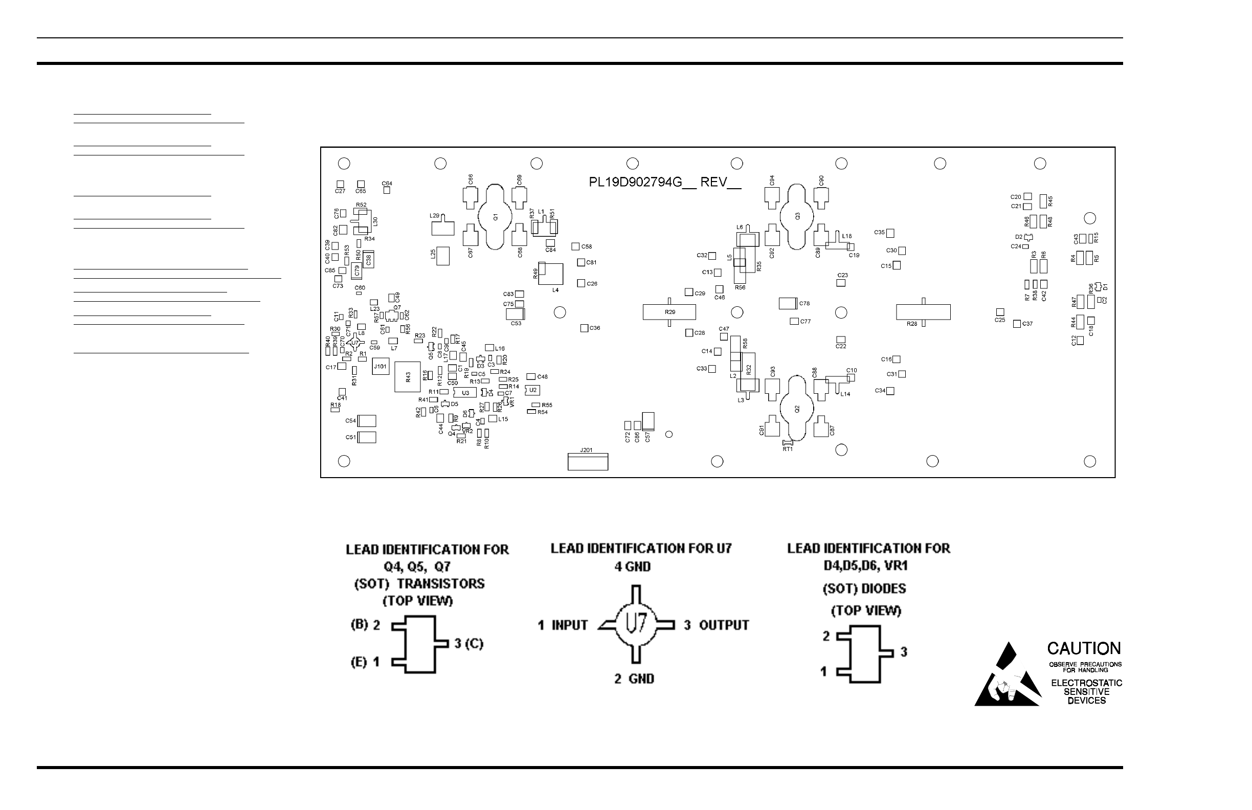
PRODUCTION CHANGES AND OUTLINE DIAGRAM
POWER AMPLIFIER BOARD A1
19D902856G3, G6, G7, G8, G9, G10 & G11
(19D902794 Sh. 2, Rev. 14)
COMPONENT SIDE
PRODUCTION CHANGES - CONT.
REV. C POWER AMPLIFIER 19D902797G3
POWER AMPLIFIER BOARD 19D902794G3
To update PWB for new band splits.
REV. D POWER AMPLIFIER 19D902797G3
POWER AMPLIFIER BOARD 19D902794G3
To update PWB for new band splits and add power
monitor circuitry.
Added U2, C48, R54, R53, R55.
REV. A POWER AMPLIFIER 19D902797G6
To update PWB to new band splits.
REV. A POWER AMPLIFIER 19D902797G7
POWER AMPLIFIER BOARD 19D902794G7
To update PWB to new band splits and add power
monitor circuitry.
Added U2, C48, R54, R53, R55.
REV. A POWER AMPLIFIER 19D902797G8, G9, G11
POWER AMPLIFIER BOARD 19D902794G8, G9, G11
REV. B POWER AMPLIFIER 19D902797G6, G7
POWER AMPLIFIER BOARD 19D902794G6, G7
REV. E POWER AMPLIFIER 19D902797G3
POWER AMPLIFIER BOARD 19D902794G3
To update PWB to new band splits for 492-512 MHz.
REV. B POWER AMPLIFIER BOARD 19D902797G11
Improve reliability.
C67 was 39 pF (19A700006P50).
LBI-38674F
10
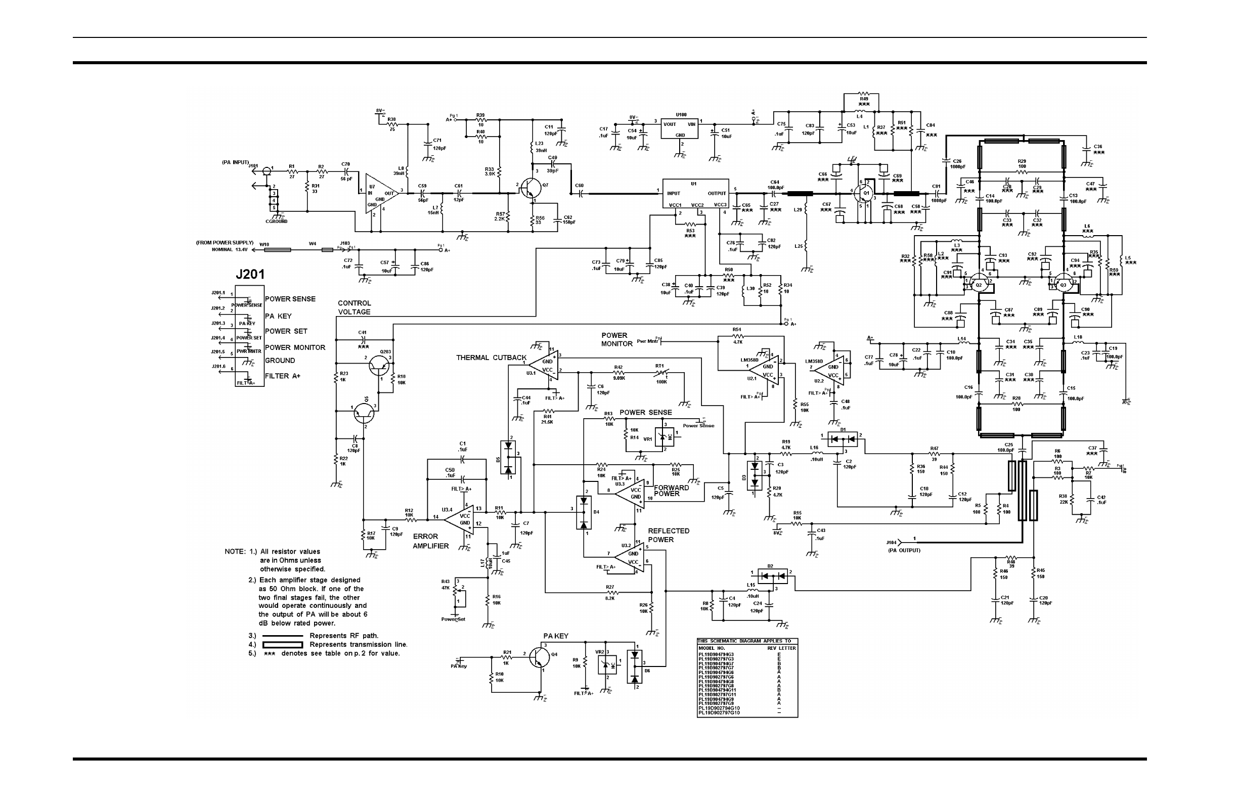
SCHEMATIC DIAGRAM
POWER AMPLIFIER ASSEMBLY
19D902797G3, G6, G7, G8, G9, G10 & G11
(19D903622 Sh. 1, Rev. 11)
LBI-38674F
11
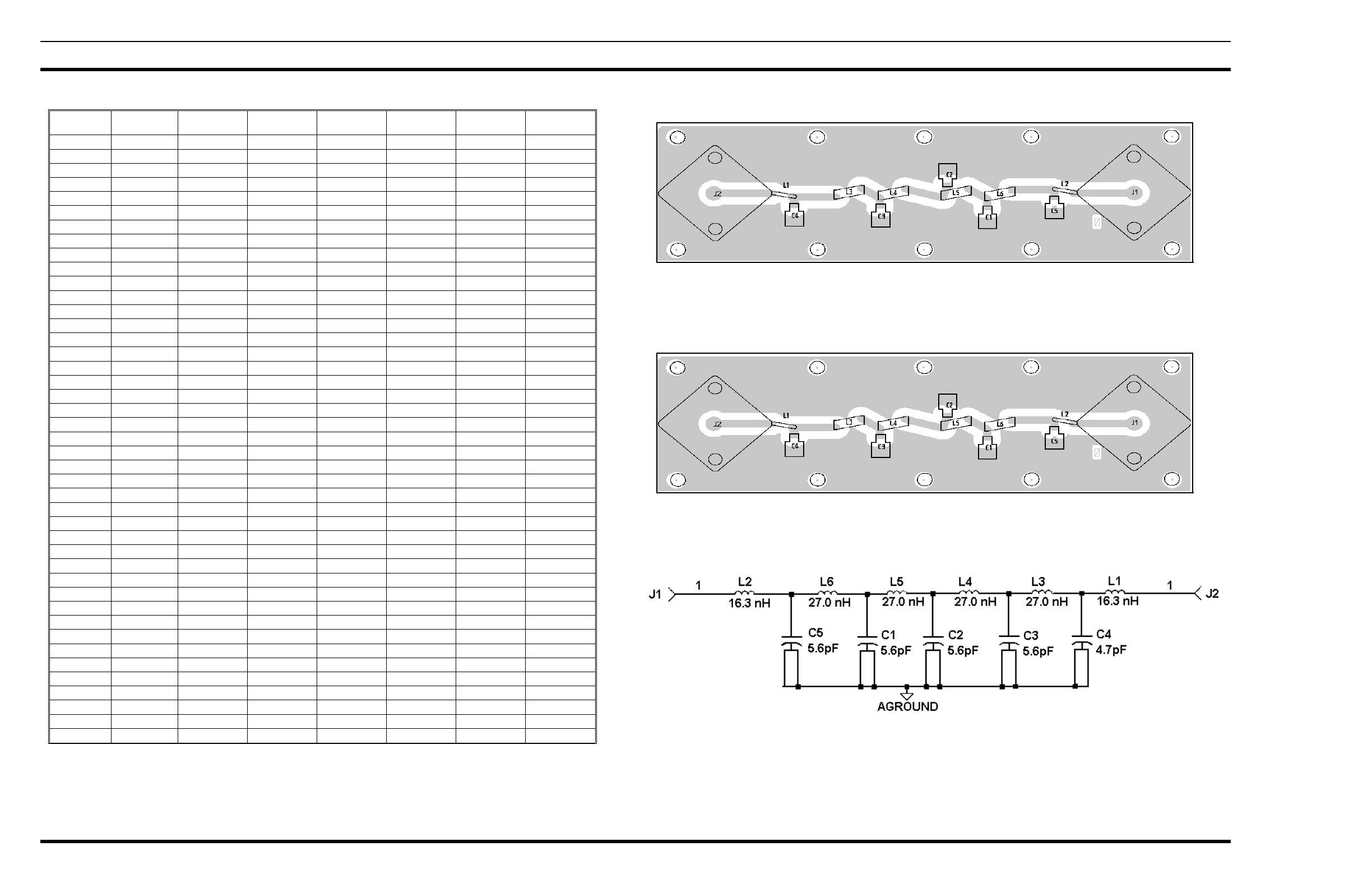
OUTLINE AND SCHEMATIC DIAGRAMS
LOW PASS FILTER MODULE
19D902856G3
(19D903623 Sh.1, Rev. 1)
(19D902853, Sh. 2, Rev. 0)
(19D903638, Component Side, Rev. 0)
COMPONENT SIDE
(19D902853, Sh. 2, Rev. 0)
(19D903638, Solder Side, Rev. 0)
SOLDER SIDE
REF. DES. 380-400 MHz403-425 MHz 425-450 MHz 450-470 MHz 470-494 MHz 492-512 MHz 410-430 MHz
C27 10.0 pf 12.0 pf 10.0 pf not used not used not used 12.0 pf
C28 15.0 pf 12.0 pf 8.2 pf not used not used not used 10.0 pf
C29 15.0 pf 12.0 pF 8.2 pF not used not used not used 10.0 pf
C30 12.0 pF not used not used 8.2 pF 8.2 pF 8.2 pF not used
C31 12.0 pF not used not used 8.2 pF 8.2 pF 8.2 pF not used
C32 not used not used not used 3.3 pF not used not used not used
C33 not used not used not used 3.3 pF not used not used not used
C34 not used 15.0 pF 15.0 pF not used not used not used 15.0 pF
C35 not used 15.0 pF 15.0 pF not used not used not used 15.0 pF
C36 3.9 pF 4.7 pF not used not used not used not used 4.7 pF
C58 12.0 pF 12.0 pF 12.0 pF 8.2 pF 5.6 pF 5.6 pF 12.0 pF
C65 not used not used not used 8.2 pF 4.7 pF 4.7 pF not used
C66 47.0 pF 39.0 pF 39.0 pF 33.0 pF 27.0 pF 27.0 pF 39.0 pF
C67 47.0 pF 47.0 pF 39.0 pF 36.0 pF 27.0 pF 27.0 pF 47 pF
C68 47.0 pF 39.0 pF 39.0 pF 33.0 pF 27.0 pF 22.0 pF 39.0 pF
C69 47.0 pF 47.0 pF 39.0 pF 36.0 pF 27.0 pF 22.0 pF 43.0 pF
C87 56.0 pF 47.0 pF 43.0 pF 39.0 pF 33.0 pF 33.0 pF 47.0 pF
C88 51.0 pF 51.0 pF 43.0 pF 39.0 pF 33.0 pF 33.0 pF 51.0 pF
C89 51.0 pF 51.0 pF 43.0 pF 39.0 pF 33.0 pF 33.0 pF 51.0 pF
C90 56.0 pF 47.0 pF 43.0 pF 39.0 pF 33.0 pF 33.0 pF 47.0 pF
C91 51.0 pF 47.0 pF 36.0 pF 33.0 pF 33.0 pF 33.0 pF 43.0 pF
C92 51.0 pF 43.0 pF 39.0 pF 33.0 pF 27.0 pF 27.0 pF 43.0 pF
C93 51.0 pF 43.0 pF 39.0 pF 33.0 pF 27.0 pF 27.0 pF 43.0 pF
C94 51.0 pF 47.0 pF 36.0 pF 33.0 pF 33.0 pF 33.0 pF 43.0 pF
L2 BEAD BEAD BEAD not used not used not used BEAD
L3 AIR COIL AIR COIL AIR COIL not used not used not used AIR COIL
L5 BEAD BEAD BEAD not used not used not used BEAD
L6 AIR COIL AIR COIL AIR COIL not used not used not used AIR COIL
R32 not used not used not used 2.2 pF 2.2 pF not used not used
R35 not used not used not used 2.2 pF 2.2 pF not used not used
C37 2.2 pF not used not used not used not used not used not used
R53 not used 0 0 0 not used not used not used
R50 0 not used not used not used 0 0 0
C41 not used not used not used not used not used not used 100.0 pF
C46 not used not used not used not used 8.2 pF 10.0 pF not used
C47 not used not used not used not used 8.2 pF 10.0 pF not used
R58 not used not used not used not used not used 4.7 pF not used
R59 not used not used not used not used not used 4.7 pF not used
R49 100 100 100 100 100 not used 100
R37 330 330 330 330 330 not used 330
R51 330 330 330 330 330 not used 1200 pF
C84 1200 pF 1200 pF 1200 pF 1200 pF 1200 pF not used 1200 pF
L1 3 turn 3 turn 3 turn 3 turn 3 turn 1 turn 3 turn
POWER AMPLIFIER ASSEMBLY
19D902797G3, G6, G7, G8, G9,G10 & G11
(19D903622 Sh.2 Rev. 11)
TABLE I
LBI-38674F
12
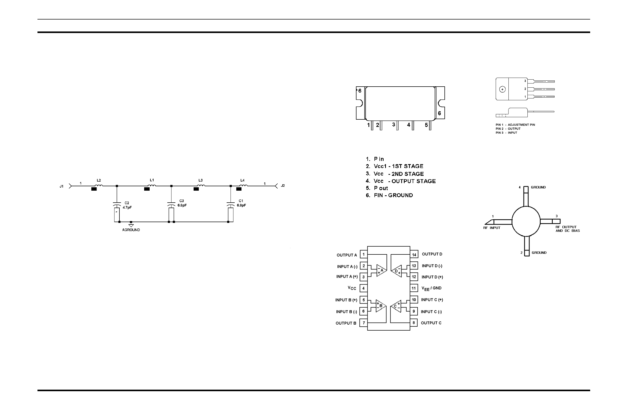
SCHEMATIC DIAGRAM & IC DATA
U1
19A705457P1, P2 AND P4
PA Amplifier Module
U3
19A701789P4
Quad Op-Amp
U100
19A705532P2
Voltage Regulator
U7
344A3907P1
MMIC Amplifier
LOW PASS FILTER MODULE
470 - 512 MHz
19D902856G9
(19B804157, Rev. 0)
LBI-38674F
13

LBI-38675E
Maintenance Manual
MASTR® III
RF PACKAGE, UHF
380-512 MHz
TABLE OF CONTENTS
TRANSMIT SYNTHESIZER . . . . . . . LBI-38671
RECEIVE SYNTHESIZER . . . . . . . . LBI-38672
RECEIVE RF MODULE . . . . . . . . . . LBI-38673
LBI-39129
IF MODULE . . . . . . . . . . . . . . . . LBI-38643
LBI-39123
POWER AMPLIFIER . . . . . . . . . . . LBI-38674
ericssonz

Copyright© July 1992, Ericsson GE Mobile Communications, Inc.
TABLE OF CONTENTS
Page
CONVENTIONAL
OPTIONS AND ACCESSORIES . . . . . . . . . . . . . . . . . . . . . . . . . . . . . . . . . . 3
ADDITIONAL OPTIONS . . . . . . . . . . . . . . . . . . . . . . . . . . . . . . . . . . . . . . 3
TONE & DC REMOTE CONTROLLED STATIONS . . . . . . . . . . . . . . . . . . . . . . . 3
REGULATORY DATA
EDACS AND CONVENTIONAL . . . . . . . . . . . . . . . . . . . . . . . . . . . . . . . . . 4
GENERAL . . . . . . . . . . . . . . . . . . . . . . . . . . . . . . . . . . . . . . . . . . . . . . 5
TRANSMITTER . . . . . . . . . . . . . . . . . . . . . . . . . . . . . . . . . . . . . . . . . . . 6
RECEIVER . . . . . . . . . . . . . . . . . . . . . . . . . . . . . . . . . . . . . . . . . . . . . 6
MODULE NUMBERS . . . . . . . . . . . . . . . . . . . . . . . . . . . . . . . . . . . . . . . 7
ANTENNA SWITCH . . . . . . . . . . . . . . . . . . . . . . . . . . . . . . . . . . . . . . . . 9
ILLUSTRATIONS
FIGURE 1 - 69" & 37" CABINET MOUNT . . . . . . . . . . . . . . . . . . . . . . . . . . . . 8
This manual covers Ericsson and General Electric products manufactured and sold by Ericsson Inc.
NOTICE!
This manual is published by Ericsson Inc., without any warranty. Improvements and changes to this manual necessitated
by typographical errors, inaccuracies of current information, or improvements to programs and/or equipment, may be
made by Ericsson Inc., at any time and without notice. Such changes will be incorporated into new editions of this manual.
No part of this manual may be reproduced or transmitted in any form or by any means, electronic or mechanical, including
photocopying and recording, for any purpose, without the express written permission of Ericsson Inc.
The software contained in this device is copyrighted by the Ericsson Inc. Unpublished rights are reserved under the
copyright laws of the United States.
NOTICE!
Repairs to this equipment should be made only by an authorized service technician or facility designated by the supplier.
Any repairs, alterations or substitution of recommended parts made by the user to this equipment not approved by the
manufacturer could void the user’s authority to operate the equipment in addition to the manufacturer’s warranty.
NOTICE!
LBI-38675E
2

CONVENTIONAL OPTIONS and ACCESSORIES
Programmable Options
• Transmit Frequencies
• Receive Frequencies
• Channel Spacing
• Channel Guard Digital and Tone
• Channel Guard Disable
• Repeater Disable
• Intercom Function
• Type 90
• DTMF Decode
• Morse Code ID
• Squelch Tail Elimination (STE)
• Carrier Control Timer
• Station Control
• DC Control
• Tone Control
• Repeater
• DC/Repeat
•Tone/Repeat
• 2 or 4 Wire Audio
• Scan
Additional Options
• Service Microphone
• Antenna Multicoupler
• 50 Hz Power Supply
• Duplexer
• Antenna Relay (VHF/UHF)
• Combiner
• Isolator
• Squelch Operated Relay
• Remote Controllers
• Battery Standby (VHF/UHF)
• Battery Charger (VHF/UHF)
• Gel Cell Battery (VHF/UHF)
• Voice Guard Encryption
• Aegis Digital
CONVENTIONAL TONE & DC REMOTE CONTROLLED STATIONS
AUDIO (Line to Transmitter)
Line Terminating Impedance: 600 W
Line Level (Adjustble): -20 dBm to +7 dBm
Frequency Response: ± 3 dB @ 300-3000 Hz
TONE CONTROL
Function Tones: 1050,1150,1250,1350,1450,
1550,1650, 1750,1850,1950 & 2050 Hz
Secur-it Tone & Transmit Tone: 2175 Hz
Transmitted 2175 Hz Tone Level: 20 dB Below Voice
Permissible Control Line Loss
@2175 Hz: 30 dB
Continued
LBI-38675E
3
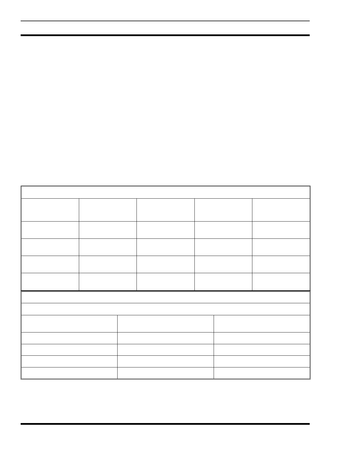
CONVENTIONAL TONE & DC REMOTE CONTROLLED STATIONS - Cont.
AUDIO (Receiver-to-Line)
Audio Amplifier Input Impedance: 10 KΩ
Input Level: 1 V RMS (For 5 kHz Deviation)
Output Impedance to Line: 600 Ω
Output Level to Line Voice (1 kHz ref): +7 dBm (Adjustable)
Tone (1 kHz ref): +7 dBm (Ref. 7 dBm)
Freqency Response: +1 dB and -3dB @ 300-3000 Hz
Hum and Noise, Noise Squelch: -55 dB (Ref. 7 dBm)
Tone Squelch: -30 dB (Ref. 7 dBm)
DC CONTROL Control Control Currents: -2.5, ± 6 & ± 11 mA
Line Loop Resistance (maximum): 11 KΩ (Includes 3K Termination)
REGULATORY DATA EDACS and CONVENTIONAL
FCC FILING DATA (for cabinet or open rack mounting)
FREQUENCY
BAND POWER OUTPUT
(Internally Adjustable)
FREQ. STABILITY
AND MODULATION
TYPE
APPLICABLE
TO FCC RULES PART
NUMBERS
FCC
FILLING
NUMBER
403-430 45 to 90 W (Freq. Mod. PLL Exc.)
1.0 PPM 22,90,80,74 AXATR-307-A
425-450 45 to 90 W (Freq. Mod. PLL Exc.)
1.0 PPM 22,90,80,74 AXATR-307-A2
450-470 50 to 100W (Freq. Mod. PLL Exc.)
1.0 PPM 22,90,80,74 AXATR-307-B2
470-494
492-512 45 to 90 W (Freq. Mod. PLL Exc.)
1.0 PPM 22,90,80,74 AXATR-307-C2
AXATR-307-D2
DOC FILING DATA
FREQUENCY
BAND TYPE NUMBER APPLICABLE SPEC
403-430 TR-307 RSS-119
425-450 TR-307 RSS-119
450-470 TR-307 RSS-119
470-494, 492-512 NA NA
LBI-38675E
4
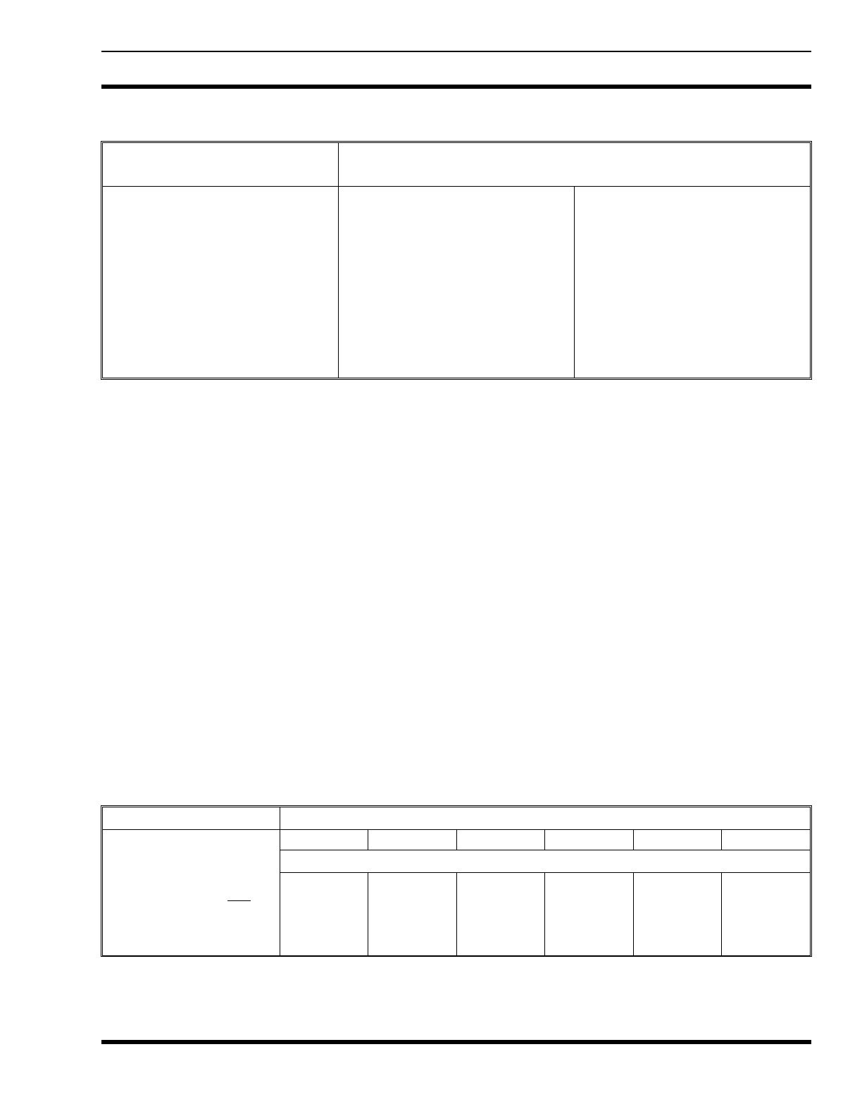
GENERAL
CABINET INDOOR CABINET (Floor Mount)
37" (CNV) 69"
SIZE [in. (mm)]
Height:
Width:
Depth:
Weight (min) [(lb. (Kg)]
Continuous Duty
Packed , Domestic Shipping
Number of Rack Units
Maximum Units w/Power Supply
Maximum Units w/o Power Supply
37.0 (940)
21.5 (550)
18.25 (460)
150 (68)
165 (75)
17
2
2
69.1 (1750)
23.1 (590)
21 .0 (533)
300 (136)
317 (147)
33
3
4
SERVICE SPEAKER: 1 Watt @ 8Ω
SERVICE MICROPHONE: Transistorized Dynamic
DC 5A @ 120 VAC or 3A @ 230 VAC
DUTY CYCLE (EIA) Continuous: Transmit/Receive - 100%
AMBIENT TEMPERATURE: -30oC to +60oC
(or full spec performance per EIA) (-22oF to +140oF)
HUMIDITY (EIA): 90% @ 50oC (122oF)
INPUT POWER SOURCE: 120 VAC (± 20%) or
Optional: 230 VAC (± 15%), 50 Hz
Standby Battery Source: 13.8 VDC, 100 AH (min.)
ANTENNA CONNECTIONS: Type N
LENGTH OF AC POWER CABLE: 10 ft (3048mm)
METERING: Provided through Handset or
TQ0619 Utility Software.
ALTITUDE
Operable: Up to 15,000 ft (4,570 m)
Shipable: Up to 50,000 ft (15,250 m)
SOURCE POWER DRAIN UHF
Frequency Range(MHz) 380-400 403-430 425-450 450-470 470-494 492-512
AC Input Power: 5A @ 120 VAC or 3A @ 230 VAC
DC Input Power: VDC
Tx (full / half power): 13.8
Rx only: 13.8
Tx (full / half power): 26.4
EDACS Applications: 13.8
33/25A
2 A
2 A
33/25A
2 A
2 A
33/25A
2 A
2 A
33/25A
2 A
2 A
33/25A
2 A
2 A
33/25A
2 A
2 A
NOTE: One Rack Unit equals 1.75 inches, Stations occupy 8 rack units of cabinet space.
LBI-38675E
5
TRANSMITTER
UHF
FREQUENCY RANGE
(MHz)
RATED POWER
OUTPUT (Watts):
RF OUTPUT
IMPEDANCE (W):
CONDUCTED SPURIOUS
& HARMONIC
EMISSION (dBm):
FREQUENCY STABILITY
(%):
MODULATION
DEVIATION (kHz):
16F3 & 16F9
20F5Y & 20F9Y
(VHF & UHF)
FM NOISE (dB):
CHANNEL STEPS (kHz)
FREQUENCY SPREAD
Full Spec (MHz)
380-400 403-430 425-450 450-470 470-494 492-512
75
50
-36
±0.0001
0 to ± 5
-55
6.25
20
90
50
-36
±0.0001
0 to ± 5
-55
6.25
22
90
50
-36
±0.0001
0 to ± 5
-55
6.25
25
100
50
-36
±0.0001
0 to ± 5
-55
6.25
20
90
50
-36
±0.0001
0 to ± 5
-55
6.25
24
90
50
-36
±0.0001
0 to ± 5
-55
6.25
20
RECEIVER
UHF
FREQUENCY RANGE
(MHz)
RF INPUT
IMPEDANCE (W):
CHANNEL SPACING
(kHz):
SENSITIVITY (dBm)
EIA 12 dB SINAD:
Threshold Squelch (dBm):
SELECTIVITY EIA 2-Signal (dB)
12.5 kHz:
25 kHz:
380-400 403-430 425-450 450-470 470-494 492-512
50
12.5/25
-115
(0.40 µV)
-118
(0.28 µV)
-80
-90
50
12.5/25
-116
(0.35 µV)
-119
(0.25 µV)
-80
-90
50
12.5/25
-116
(0.35 µV)
-119
(0.25 µV)
-80
-90
50
12.5/25
-116
(0.35 µV)
-119
(0.25 µV)
-80
-90
50
12.5/25
-116
(0.35 µV)
-119
(0.25 µV)
-80
-90
50
12.5/25
-116
(0.35 µV)
-119
(0.25 µV)
-80
-90
Continued
AUDIO DISTORTION (@ 1 kHz): Less than 3%
NUMBER OF CHANNELS (Conventional): up to 16
AUDIO RESPONSE (pre-emphasis): Within +1 and -3 dB of 6dB/octave,
300 to 3000 Hz per EIA.
NOTE: Rated power output is measured at the transmitter power amplifier output connector per FCC Type Acceptance filling
information. Any customer- required optional items such as power measuring devices and/or duplexers will introduce loss
between the transmitter output connector and the station cabinet output connector. This loss will reduce the available power
at the station connector.
LBI-38675E
6
RECEIVER - Cont.
UHF
FREQUENCY RANGE
(MHz)
FREQUENCY STABILITY
(%):
SIGNAL DISPLACEMENT
BANDWIDTH (kHz):
INTERMODULATION (dB)
12.5 kHz:
25 kHz:
30 kHz:
ETSI
SPURIOUS & IMAGE
REJECTION (dB):
FREQUENCY SPREAD
Full Specs. (MHz):
3 dB Degradation in
Sensitivity (MHz):
380-400 403-430 425-450 450-470 470-494 492-512
±0.0001
±2
-80
-85
-100
2.0
3.0
±0.0001
±2
-80
-85
-100
2.0
3.0
±0.0001
±2
-80
-85
-100
2.0
3.0
±0.0001
±2
-80
-90
-85
-100
2.0
3.0
±0.0001
±2
-80
-90
-100
2.0
3.0
±0.0001
±2
-80
-90
-100
2.0
3.0
AUDIO RESPONSE (de-emphasis): Within +2 and -8 dB of 6 dB/octave
(@ Local Speaker), 300 to 3000 Hz per EIA.
Within +1 and -3 dB of 6 dB/octave
(@ Line Output), 300 to 3000 Hz per EIA.
AUDIO OUTPUT: 1 Watt at less than 3% distortion @ 1000 Hz,
25 kHz Channel
MODULE NUMBERS
TRANSMIT SYNTHESIZER (450-470 MHz) ........................................19D902780G3
(425-450 MHz) ........................................19D902780G7
(403-425 MHz, 410-430MHz)................19D902780G6
(380-400 MHz) ........................................19D902780G8
(470-494 MHz) ........................................19D902780G9
(492-512 MHz) .......................................19D902780G10
RECEIVE SYNTHESIZER (450-470 MHz, 403-425 MHz,
410-430 MHz)..........................................19D902781G3
(425-450 MHz, 470-494 MHz)...............19D902781G7
(380-400 MHz) ........................................19D902781G8
(492-512 MHz) .......................................19D902781G10
RX FRONT END MODULE (450-470 MHz) ........................................19D902782G3
(425-450 MHz) ........................................19D902782G7
(403-425 MHz) ........................................19D902782G6
(410-430 MHz) .......................................19D902782G11
(380-400 MHz) ........................................19D902782G8
(470-494 MHz) ........................................19D902782G9
(492-512 MHz) .......................................19D902782G10
IF MODULE ...................................................................19D902783G1
(470-494 MHz, 492-512 MHz)...............19D902783G7
Continued
LBI-38675E
7
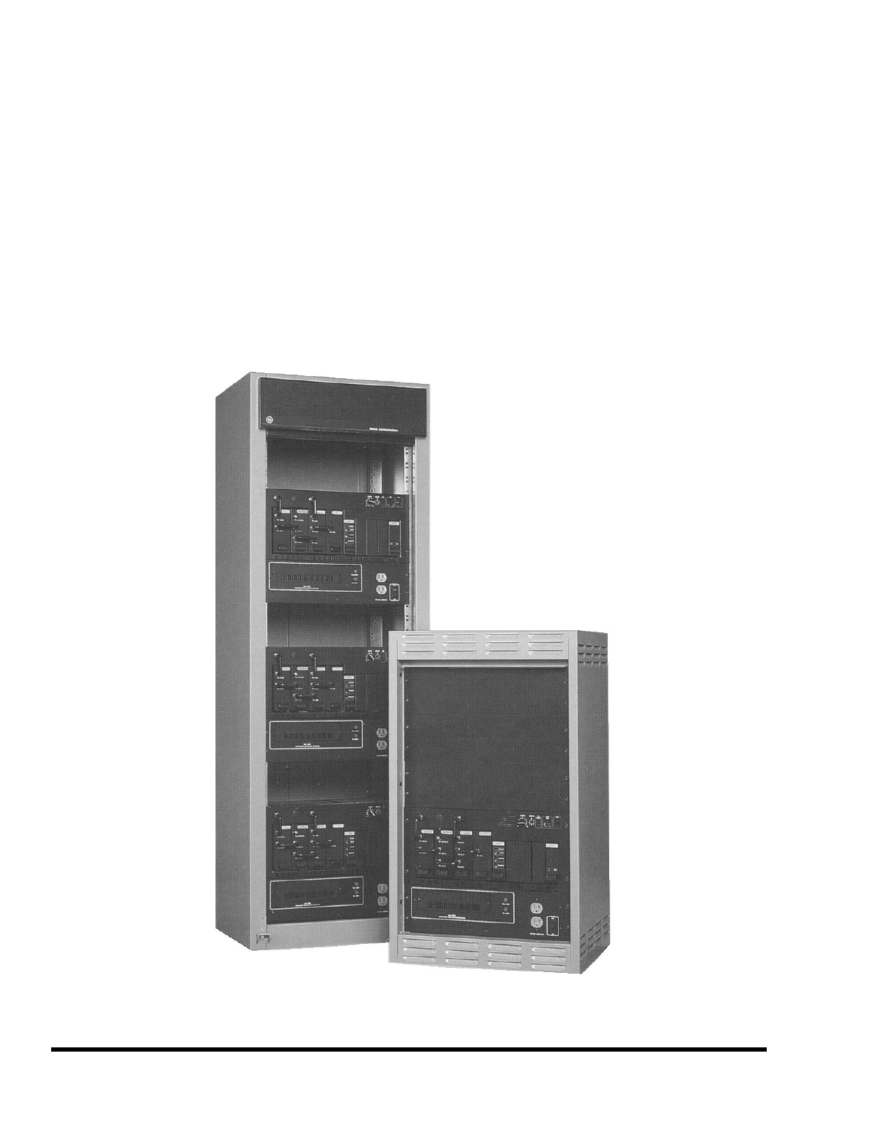
MODULE NUMBERS - Cont.
POWER AMPLIFIER (450-470 MHz).........................................19D902797G3
(425-450 MHz).........................................19D902797G7
(403-425 MHz).........................................19D902797G6
(410-430 MHz.........................................19D902797G11
(380-400 MHz).........................................19D902797G8
(470-494 MHz).........................................19D902780G9
(492-512 MHz)........................................19D902780G10
LOW PASS FILTER ...................................................................19D902856G1
(470-512 MHz).........................................19D902780G9
ANTENNA SWITCH ................................................................... 19B235897P2
DUPLEXER (440-470 MHz).......................................... 344A4047P1
Fig 1 - 69" & 37" Cabinet Mount
8
ACCESSORIES
ANTENNA SWITCH
19B235897P2
LBI-38675E
9

Ericsson Inc.
Private Radio Systems
Mountain View Road
Lynchburg, Virginia 24502
1-800-528-7711 (Outside USA, 804-592-7711) Printed in U.S.A.
LBI-38675E

MAINTENANCE MANUAL FOR
21.4 MHz RECEIVER IF MODULE
12.5/25 kHz CHANNEL SPACING
19D902783G7 & G11
DESCRIPTION
The MASTR III Receiver IF Module provides amplifi-
cation and demodulation of the 21.4 MHz Intermediate
Frequency signal. The IF Module also includes the re-
ceiver squelch circuitry. However, it does not include de-
emphasis or squelch audio gating circuits. Figure 1 is a
block diagram showing the functional operation of the IF
Module.
The IF Module circuitry contains the following:
•A 50 ohm input impedance IF Amplifier
•A chain of two crystal filters and an integrated
circuit IF amplifier
•An integrated circuit containing a crystal oscillator,
mixer, limiter, and quadrature detector
•A variable gain AF amplifier
•A squelch circuit
•A fault detector circuit
•An integrated circuit voltage regulator
•An address decoder
TABLE OF CONTENTS
Page
DESCRIPTION . . . . . . . . . . . . . . . . . . . . . . . . . . . . . . . . . . . . . . . . . . . . Front Cover
GENERAL SPECIFICATIONS . . . . . . . . . . . . . . . . . . . . . . . . . . . . . . . . . . . . 1
BLOCK DIAGRAM . . . . . . . . . . . . . . . . . . . . . . . . . . . . . . . . . . . . . . . . . 1
CIRCUIT ANALYSIS . . . . . . . . . . . . . . . . . . . . . . . . . . . . . . . . . . . . . . . . . 1
INPUT MATCHING NETWORK . . . . . . . . . . . . . . . . . . . . . . . . . . . . . . . 1
CRYSTAL FILTERS, IF AMPLIFIERS . . . . . . . . . . . . . . . . . . . . . . . . . . . . 1
OSCILLATOR/MIXER/DETECTOR . . . . . . . . . . . . . . . . . . . . . . . . . . . . . 1
AUDIO AMPLIFIER . . . . . . . . . . . . . . . . . . . . . . . . . . . . . . . . . . . . . . 1
SQUELCH . . . . . . . . . . . . . . . . . . . . . . . . . . . . . . . . . . . . . . . . . . . . 2
Buffer Amplifier . . . . . . . . . . . . . . . . . . . . . . . . . . . . . . . . . . . . 2
Bandpass Filter . . . . . . . . . . . . . . . . . . . . . . . . . . . . . . . . . . . . 2
Noise Detector . . . . . . . . . . . . . . . . . . . . . . . . . . . . . . . . . . . . . 2
DC Amplifier . . . . . . . . . . . . . . . . . . . . . . . . . . . . . . . . . . . . . 2
Schmitt Trigger . . . . . . . . . . . . . . . . . . . . . . . . . . . . . . . . . . . . 2
FAULT DETECTOR . . . . . . . . . . . . . . . . . . . . . . . . . . . . . . . . . . . . . . 2
VOLTAGE REGULATOR . . . . . . . . . . . . . . . . . . . . . . . . . . . . . . . . . . . 2
ADDRESS DECODER . . . . . . . . . . . . . . . . . . . . . . . . . . . . . . . . . . . . . 2
MAINTENANCE . . . . . . . . . . . . . . . . . . . . . . . . . . . . . . . . . . . . . . . . . . . 2
RECOMMENDED TEST EQUIPMENT . . . . . . . . . . . . . . . . . . . . . . . . . . . . 2
ALIGNMENT PROCEDURE . . . . . . . . . . . . . . . . . . . . . . . . . . . . . . . . . 2
TROUBLESHOOTING . . . . . . . . . . . . . . . . . . . . . . . . . . . . . . . . . . . . . 3
ASSEMBLY DIAGRAM . . . . . . . . . . . . . . . . . . . . . . . . . . . . . . . . . . . . . . . 3
OUTLINE DIAGRAM . . . . . . . . . . . . . . . . . . . . . . . . . . . . . . . . . . . . . . . . 4
SCHEMATIC DIAGRAM . . . . . . . . . . . . . . . . . . . . . . . . . . . . . . . . . . . . . . 5
IC DATA . . . . . . . . . . . . . . . . . . . . . . . . . . . . . . . . . . . . . . . . . . . . . . . . 10
PARTS LIST . . . . . . . . . . . . . . . . . . . . . . . . . . . . . . . . . . . . . . . . . . . . . . 11
PRODUCTION CHANGES . . . . . . . . . . . . . . . . . . . . . . . . . . . . . . . . . . . . . Back Cover
LBI-39123E
ERICSSONZ
Ericsson Inc.
Private Radio Systems
Mountain View Road
Lynchburg, Virginia 24502
1-800-528-7711 (Outside USA, 804-592-7711) Printed in U.S.A.
PRODUCTION CHANGES
Changes in the equipment to improve performance or to simplify
circuits are identified by a "Revision Letter" which is stamped after the
model number of the unit. The revision stamped on the unit includes all
previous revisions. Refer to the Parts List for the descriptions of parts
affected by these revisions.
REV. B - RECEIVER IF MODULE 19D902494G7
To improve production of Group 7 boards.
New schematic (193D1065).
REV. A - RECEIVER IF MODULE 19D902494G11
To ensure correct operation, U7 (19A701789P4) was replaced.
REV. B - RECEIVER IF MODULE 19D902494G11
To increase margins on squelch threshold sensitivity and 12 dB
SINAD in 12.5 kHz mode. C86 was 0.01 µF (19A702052P14),
R6 was 50 ohms (19B800607P510), R97 was 39 ohms
(19B801251P390) and R98 and R99 were 150 ohms
(19B801251P151). Added L6 (19A705430P24).
CIRCUIT ANALYSIS
INPUT AMPLIFIER NETWORK
The input amplifier, consisting of Q2 and T1, provides a
50 ohm load for the receiver RF module.
Capacitor C1 provides AC coupling and a DC block on
the input line (J1). This DC block protects the module in the
event of a failure in a preceding module.
C1 and L9 are series-resonant at 21.4 MHz and provide a
low-impedance path from J1 to amplifier Q2. C89 and L8
are parallel-resonant at 21.4 MHz and provide a path to the
50-ohm lead, R105, for mixer products other than 21.4
MHz.
CRYSTAL FILTERS, IF AMPLIFIERS
Y1, Y2, U1, and associated circuitry provide IF filtering
and amplification at 21.4 MHz. Filters Y1 and Y2 are both 4-
pole bandpass filters with a center frequency of 21.4 MHz
and a bandwidth of ±6.5 kHz. Amplifier UI is an integrated-
circuit amplifier. U1 provides 30 dB of gain. The amplifier
and filters have terminal impedances of 50 ohms. In-circuit
gain measurements can be made using a high impedance
probe.
Inductors L3, L5 and associated resistors and capacitors
provide power supply decoupling. R3 provides a path to the
input of the Fault Detector circuit. This input enables the
Fault Detector circuit to monitor the DC voltage of U1.
The RF level detector consists of transistor Q1 along
with associated resistors and capacitors. This detector plays
no role in the normal operation of the IF Module, but aids in
unit testing and module troubleshooting.
OSCILLATOR/MIXER/DETECTOR
Integrated circuit U3 provides several functions includ-
ing 2nd mixer, if amplifier and limiter, and quadrature detec-
tor.
The 20.945 MHz crystal oscillator provides local oscilla-
tor injection to the mixer in U3. This mixer converts the 21.4
MHz IF signal to 455 kHz. C20 and C21 are oscillator feed-
back capacitors and have been chosen to provide the proper
capacitance for crystal Y3. The proper oscillator output level
is difficult to measure directly without affecting the oscilla-
tion.
A preferable measurement is at TP3 which should read
about 10 mV pk. (Measured using a 10 megohm 11 pF oscil-
loscope probe.)
The mixer is internally connected to the crystal oscillator.
Pins 1 and 20 of U3 are the mixer input and output respec-
tively. Typical mixer conversion loss is about 2 dB.
In the 12.5 kHz mode, the output of the mixer drives the
IF amplifier via analog switch U11-2, filter FL1 and analog
switch U11-3. In the 25 kHz mode, the mixer output is
routed through analog switch U11-1 and C85 to the IF am-
plifier. The analog switches are controlled by the signal at
point ’A’; high for 25 kHz, low for 12.5 kHz.
The IF amplifier output drives the limiter via the 6-pole
ceramic filter FL2.
A received-signal-strength indicator (RSSI) is provided
at U3 Pin 7. This indicator signal is generated within the
limiter circuitry and provides an output current proportional
to the logarithm of the input signal strength. This current de-
velops a voltage across R18. The voltage varies from about 1
Vdc for noise input, to about 1.4 Vdc for a 12 dB SINAD
signal, to a maximum of about 4.8 Vdc for a high signal
level (70 dB stronger than that required for 12 dB SINAD).
The quadrature detector provides a demodulated audio
frequency output. The input to the detector is internally con-
nected to the limiter and is not externally available. The out-
put of the detector is U3 pin 9. C28 provides low-pass
filtering to remove 455 kHz feedthrough. Ceramic resonator
Y4 provides the frequency selective component needed for
FM demodulation. Y4 replaces the typical LC resonant cir-
cuit found in most quadrature detectors. In contrast to the
typical LC network, Y4 requires no adjustment.
The DC supply to U3 is provided through voltage drop-
ping resistor R11 to U3 pin 6. R12 provides a path to the in-
put of the Fault Detection circuit. This enables the Fault
Detector to monitor the DC voltage on U3.
AUDIO AMPLIFIER
Operational amplifier U6.3 provides audio frequency
amplification. Its gain is set by its associated resistors, in-
cluding variable resistor VR1. VR1 allows for adjusting the
AF output level to 1 Vrms with a standard input signal to the
module (1 kHz AF, 3 kHz peak deviation). In the 12.5 kHz
mode, the demodulated audio is at a lower level than in the
25 kHz mode. The gain of amplifier U6.3 is, therefore, in-
creased to give the same 1V rms output with a standard input
signal to the module of 1.5 kHz deviation. This is done by
transistor switch Q6 connecting R1 across R40. U6.2 is
used as a voltage regulator to provide 4 Vdc for biasing the
operational amplifier.
Copyright© November 1994, Ericsson GE Mobile Communications Inc.
TABLE 1 - GENERAL SPECIFICATIONS
ITEM SPECIFICATION
I.F. frequency
Input Impedance
l2 dB SINAD
Adj. CH SEL
Image
3rd order Intercept Pt
Variation of Sensitivity with Signal Frequency
2nd I.F. frequency
2nd L.O. frequency
AF output (J2 pin 31C)
AF output impedance
AF distortion
AF response
10 Hz
300 Hz
1000 Hz
3 kHz
Hum & Noise
RSSI output (J2 pin 20C)
RSSI time constant
SQ Threshold Sensitivity
SQ Maximum Sensitivity
SQ Clipping
SQ Attack
SQ Close
SQ output (J2 pin 26C)
Fault output (J2 pin IIC)
DC Supply
21.4 MHz
50 ohm
-120 dBm (25 kHz); -119 dBm (12.5 kHz)
-90 dB (25 kHz); -80 dB (12.5 kHz)
-100 dB
23 dBm (25 kHz); 11 dBm *(12.5 kHz) *@ 50 kHz offset
2 kHz (25 kHz); 1 kHz (12.5 kHz)
455 kHz
20.945 MHz
1 Vrms adjustable (with standard input signal)
1k ohm
5% (25 kHz); 5% (12.5 kHz)
-3 dB
±1 dB
0 dB reference
±1 dB
-55 dB (25 kHz); -50 dB (12.5 kHz)
0.7 to 2.7 Vdc prop to log (sig level)
5 ms
-123 dBm (25 kHz); -122 dBm (12.5 kHz)
-110 dBm (25 kHz); -109 dBm (12.5 kHz)
3 kHz
150 ms
250 ms
5V logic (low = squelched)
5V logic (low = fault)
13.8V, 150 mA max.; 12.0V, 18 mA max.
This manual is published by Ericsson Inc., without any warranty. Improvements and changes to this manual necessitated by typographical errors,
inaccuracies of current information, or improvements to programs and/or equipment, may be made by Ericsson Inc., at any time and without no-
tice. Such changes will be incorporated into new editions of this manual. No part of this manual may be reproduced or transmitted in any form or
by any means, electronic or mechanical, including photocopying and recording, for any purpose, without the express written permission of
Ericsson Inc.
LBI-39123E
1
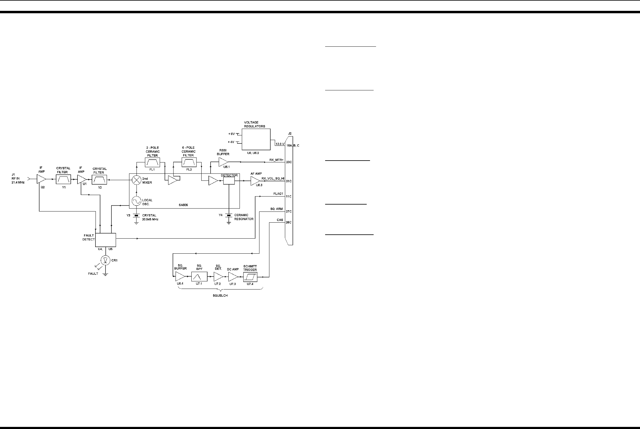
SQUELCH
Buffer Amplifier
Integrated circuit U6.4 is configured as a unity gain buffer
amplifier. It provides a high input impedance to minimize load-
ing of the previous circuits.
Bandpass Filter
The audio frequency bandpass filter consists of U7.1 and its
associated circuitry. The purpose of this filter is to reject all
voice frequencies and allow only demodulated noise to pass.
The functioning of the squelch circuit depends upon the pres-
ence or absence of this noise. (When a signal is being received,
i.e. the receiver is quiet, the squelch circuit senses the absence
of noise and unsquelches the radio.)
Noise Detector
U7.2 along with associated components act as a noise de-
tector. The rectified output of U7.2 charges C11/C44 to a
nearly constant DC voltage.
DC Amplifier
U7.3 is configured as a basic amplifier with a gain of 3.
Schmitt Trigger
U7.4 is configured as an amplifier with positive feedback.
This arrangement provides hysteresis in the output versus input
characteristic. This eliminates the possibility of the squelch cir-
cuit repeatedly cutting in and out when the input signal is near
a threshold. R56 and R57 act as a voltage divider to provide a 5
volt logic level output. (Logic High = unsquelched)
FAULT DETECTOR
U4 and U5 are voltage comparators. These are configured
into four "window detectors" which sense the presence of volt-
ages within specified ranges (windows).
The four window detector circuits are U4.1 & U4.2, U4.4
& U4.3, U5.1 & U5.2, and U5.4 & U5.3. These monitor DC
operating voltages on U6.2, U1, Q2, and U3 respectively. R29
and R30 comprise a voltage divider to provide a 5 volt logic
level output. A fault is indicated when the output drops to zero.
Diode D1 and transistor Q3 monitor the output of the 8V
regulator. DI is a 8.2 volt breakdown diode. If the regulator
output voltage should rise above 8.9 V (8.2 + 0.7 base-emitter
drop) Q1will turn on and a fault will be indicated.
Transistors Q4 and Q5 are drivers for the front panel LED
CRI. These are powered from the +13.8 Vdc line before the 8V
regulator. Therefore, if the regulator opens, a fault will still be
indicated.
VOLTAGE REGULATOR
U8 is a monolithic integrated-circuit voltage regulator pro-
viding 8 Vdc. This powers all circuitry in the module with the
exception of Q2, the front panel LED and its drivers.
ADDRESS DECODER
The address decoder consists of U2, an 8-stage shift regis-
ter, and U9, a BCD-to-decimal decoder. When A2, A1 and A0
are ’1’, ’1’, ’0’, respectively and the ENABLE line is high, Q7
on U9 goes high. This enables data input to U2 to propagate
through it, controlled by the clock pulses on U2-3. When the
ENABLE signal goes low, U9-4 goes low, and the shift-register
outputs are latched. Q1 on U2 is then high for the 12.5 kHz
mode, and low for the 25 kHz mode.
MAINTENANCE
RECOMMENDED TEST EQUIPMENT
The following test equipment is required to test the IF
Module.
1. FM Signal Generator; HP 8640B, HP 8657A, or
equivalent
2. AF Generator or Function Generator
3. Audio Analyzer; HP 8903B, HP 339A, or equivalent
4. Oscilloscope
5. Frequency Counter; Racal-Dana 9919 or equivalent
6. DC Meter for troubleshooting
7. Power Supply; 13.8 Vdc @ 150 mA
8 Power Supply; 12 Vdc @20 mA
ALIGNMENT PROCEDURE
1. Apply 13.8 Vdc and 12 Vdc supplies to module.
2. Verify 13.8 V DC current consumption is between 90
and 150 mA, and 12 Vdc current is between 12 and 18
mA.
3. Verify fault output is 0 to 0.5 Vdc and front panel LED
is off.
21.4 MHz IF MODULE - BLOCK DIAGRAM
LBI-39123E
2
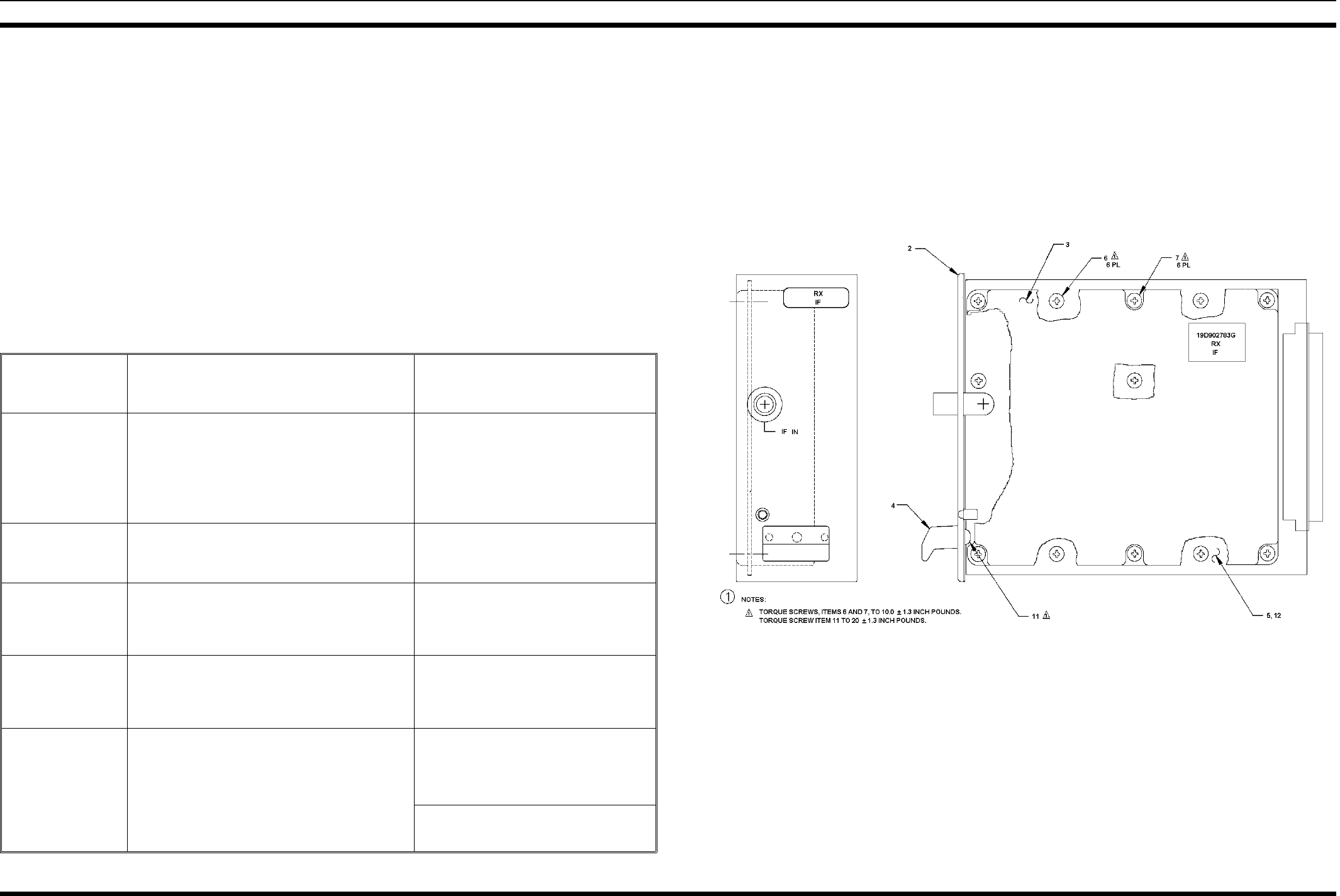
4. Apply a standard input signal to the module input. (-60
dBm, 21.4 MHz signal modulated with 1 kHz AF, 3
kHz peak deviation)
5. Monitor TP5 with a high-impedance probe connected to
the frequency counter. Adjust L10 for a reading of 455
kHz ± 100 Hz.
6. Set VRI for 1 Vrms ±3% at module output (pin 31C on
96 pin connector J2).
TROUBLESHOOTING
When troubleshooting the module, it is most convenient if
the standard test fixture is used. The following conditions are
with the module in the 25 kHz mode. This can be set up using
a PC with the necessary software connected to the test fixture.
Alternatively, a wire link can be soldered between holes H1
and H2 on the PC board.
IF amplifier Q2 has a nominal 8 dB gain. U1 has a nominal
gain of 30 dB. The mixer has about 2 dB loss with proper LO
injection. The proper crystal oscillator level is 10 mV pk meas-
ured at TP3.
The following four test points are provided on the PWB for
additional test capability:
TP1: 60 mV pk @ 21.4 MHz with -30 dBm input signal
TP3: 10 mV pk @ 20.945 MHz independent of input sig-
nal
TP4: 20 mV pk @ 455 kHz with -60 dBm input signal
TP5: 750 mV pk @ 455 kHz with -60 dbm input signal
All RF voltages measured with 10 Megohm, 11 pF probe.
ASSEMBLY DIAGRAM
TROUBLE SHOOTING GUIDE
SYMPTOM CHECK
(CORRECT READING SHOWN) INCORRECT READING
INDICATES DEFECTIVE
COMPONENT
Fault indicator on Check DC voltages
+8V at U8 Pin 1
+4v at U6 Pin 7
5.5V at U1 output pin
6V at U3 Pin 5
If DC voltages not correct
U8 or associated components
U6 or associated components
U1 or associated components
U3 or associated components
If DC voltages correct
U4, U5, U6, DI, Q3, Q4, Q5
No audio - no noise With no signal applied to module IF input
Check for AF noise @ C29 ; 200mV
Check for AF noise @ U6 Pin 14:1 V
U3 or associated components
U6 or associated components
Noise only - no
demodulated audio Check crystal oscillator: TP3 10 mVpk 20.945 MHz
Apply-30 dBm 21.4 MHz input, check TPl 60 mVpk
Apply-60 dBm 21.4 MHz input, check TP4 20 mVpk
U3, Y3 or associated components
Q2, Y1, U1 or associated components
U3, FL1 or associated components
Poor 12 dB SINAD Check crystal oscillator: TP3 10 mVpk 20.945 MHz
Apply-30 dBm 21.4 MHz input, check TP1 60 mVpk
Apply-60 dBm 21.4 MHz input, check TP4 20 mVpk
U3, Y3 or associated components
Q6, Y1, U1 or associated components
U3, FL1 or associated components
No squelch
function With squelch pot maximum, or with module AUDIO/
SQUELCH/HI connected to SQUELCH/ARM input
and with no signal to module IF input:
Check Presence of 1 Vpk noise at U6 Pin 14
Check presence of 1 Vpk noise U7 at Pin 1
Check DC voltage U7 at Pin 8: 7V
Check DC voltage U7 at Pin 14: 0.5V
U6 or associated components
U7 or associated components RECEIVER IF MODULE
19D902783G7, G11
(19D902783, Sh. 1, Rev. 3)
LBI-39123E
3
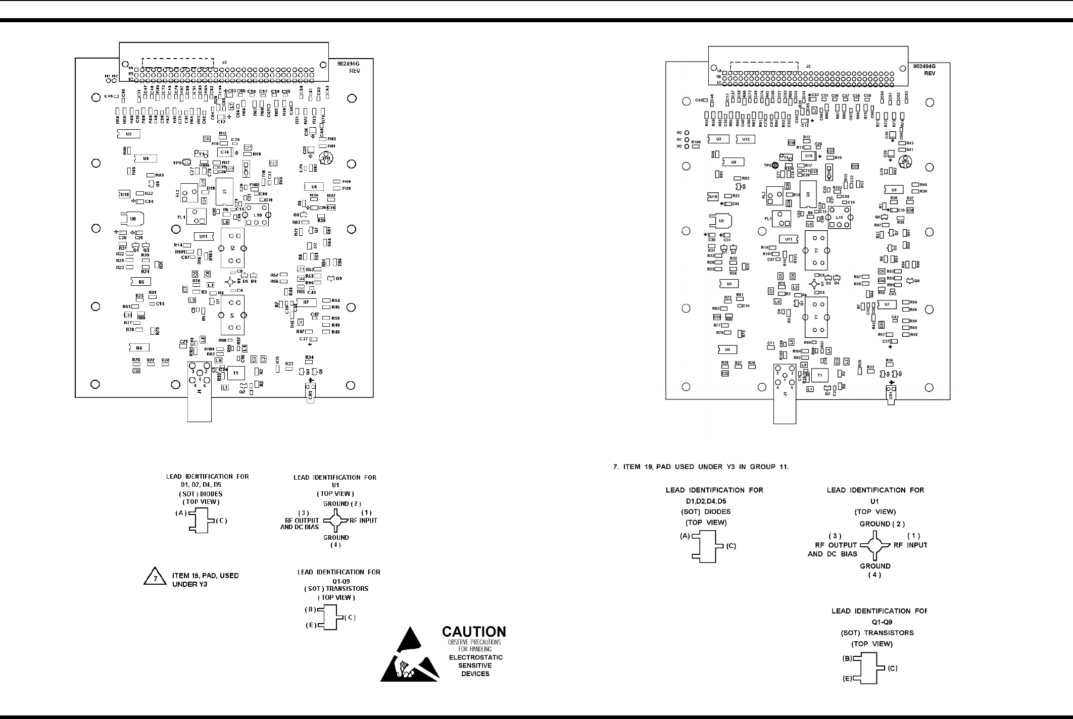
OUTLINE DIAGRAM
RECEIVER IF MODULE (EARLIER VERSION)
19D902494G7, G11
(19D902494, Sh.3, Rev. 6)
RECEIVER IF MODULE
19D902494G7 & G11
(19D902494, Sh.4, Rev. 6)
LBI-39123E
4
SCHEMATIC DIAGRAM
RECEIVER IF MODULE (EARLIER VERSION)
19D902494G7, G11
(188D5586, Sh. 1, Rev. 3)
LBI-39123E
5
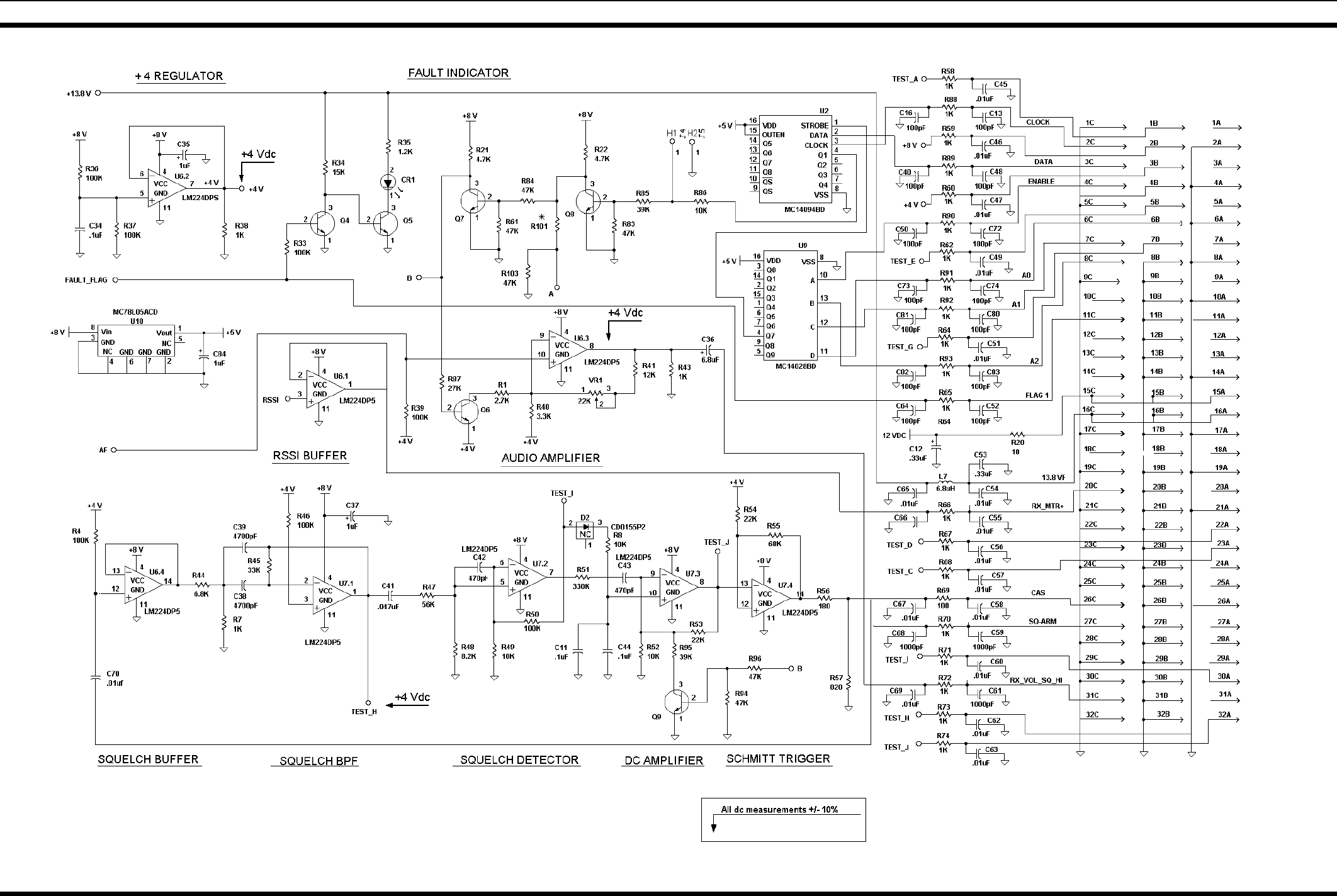
SCHEMATIC DIAGRAM
RECEIVER IF MODULE (EARLIER VERSION)
19D902494G7, G11
(188D5586, Sh. 2, Rev. 3)
LBI-39123E
6
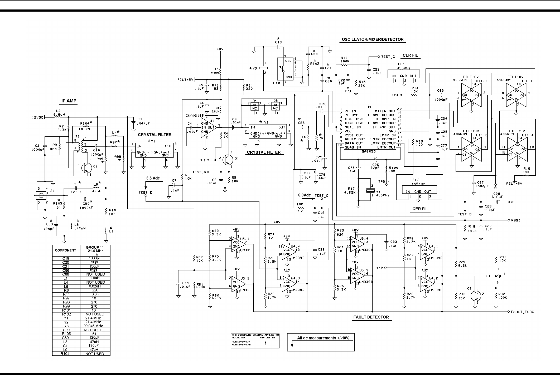
SCHEMATIC DIAGRAM
RECEIVER IF MODULE
19D902494G7 & G11
(193D1065, Sh. 1, Rev. 3)
LBI-39123E
7
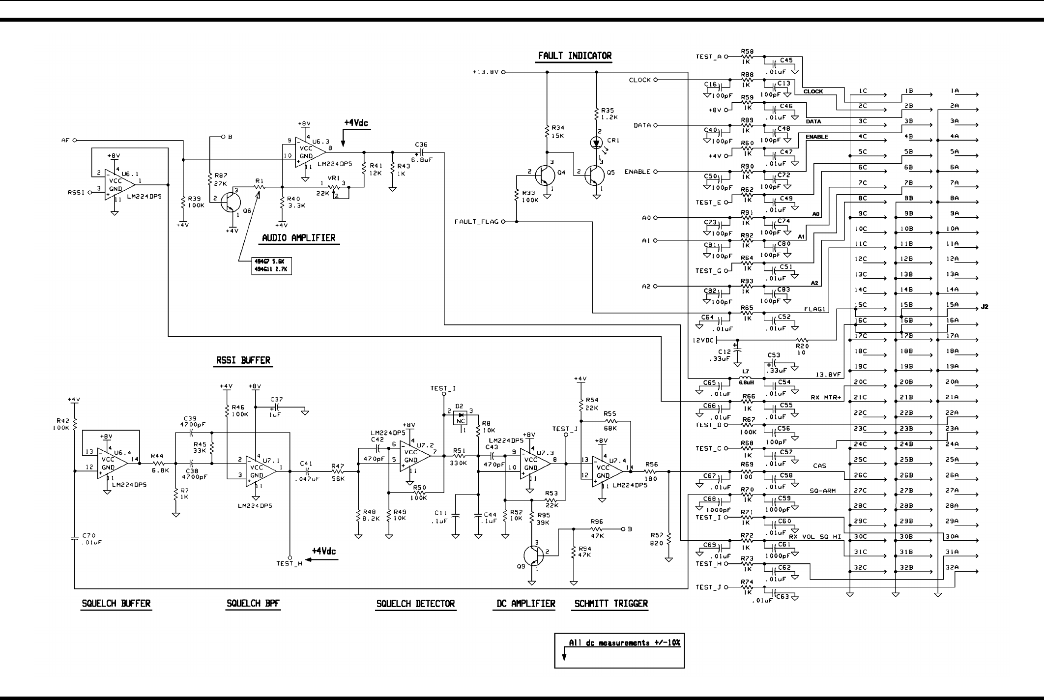
SCHEMATIC DIAGRAM
RECEIVER IF MODULE
19D902494G7 & G11
(193D1065, Sh. 2, Rev. 3)
LBI-39123E
8

SCHEMATIC DIAGRAM
RECEIVER IF MODULE
19D902494G7 & G11
(193D1065, Sh. 3, Rev. 3)
LBI-39123E
9
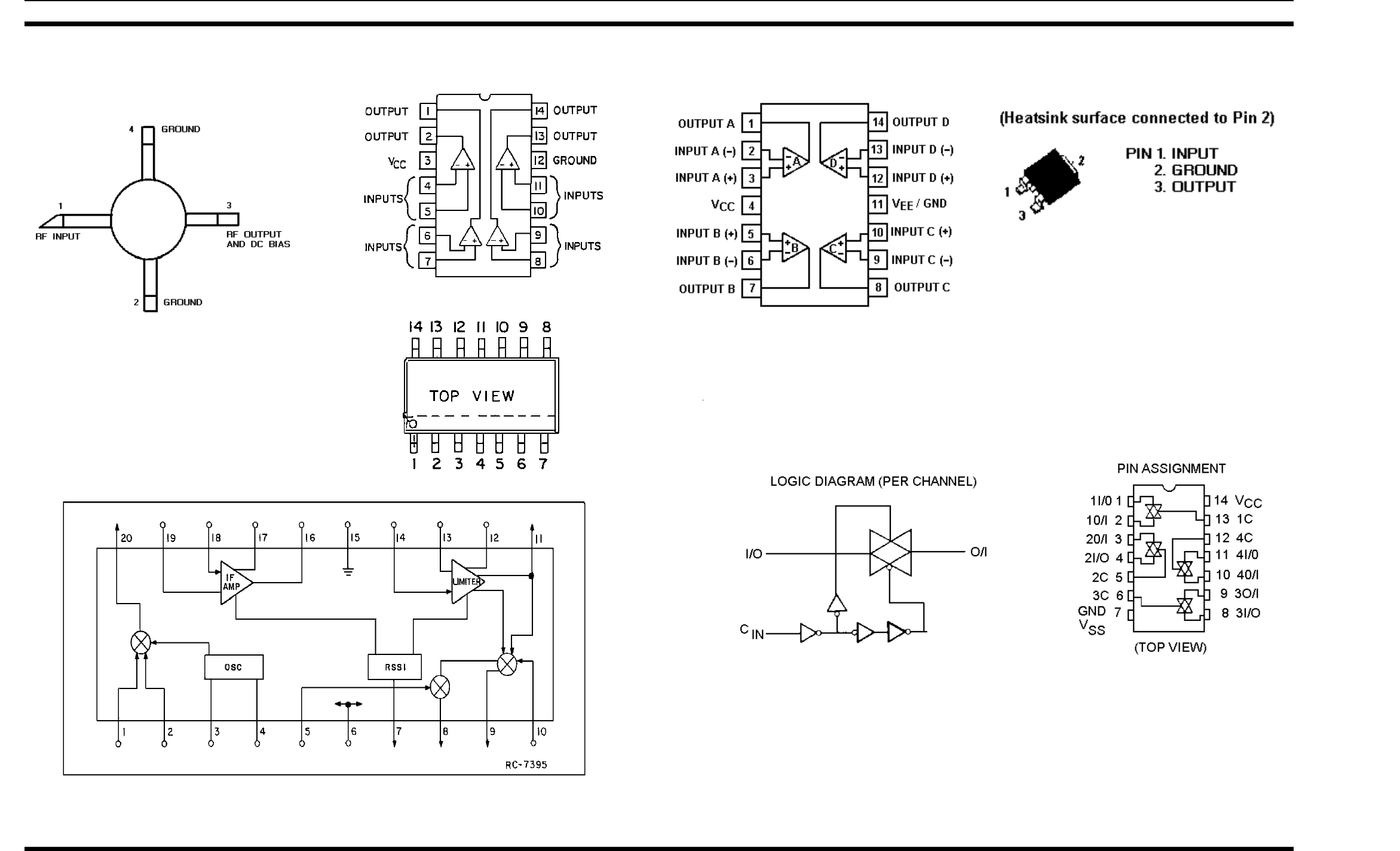
IC DATA
U1
344A3740P1
Silicon Bipolar IC
U3
19A705535P3
FM Receiver
U4 & U5
19A704125P1
kQuad Comparator
U6 & U7
19A701789P4
Quad Op-Amp
U8
19A704971P10
Voltage Regulator
U11
RYT3066018/C
Bilateral Switch
LBI-39123E
10
PARTS LIST
SYMBOL PART NUMBER DESCRIPTION
C45
thru
C47
19A702052P14 Ceramic: 0.01 µF ±10%, 50 VDCW.
C48 19A702236 P50 Ceramic: 10 0 pF ±5%, 50 VDCW, temp coef 0 ±30
PPM/°C.
C49 19A702052P14 Ceramic: 0.01 µF ±10%, 50 VDCW.
C50 19A702236P50 Ceramic: 10 0 pF ±5%, 50 VDCW, temp coef 0 ±30
PPM/°C.
C51
and
C52
19A702052P14 Ceramic: 0.01µF±10%, 50 VDCW.
C53 19A705205P12 Tantalum: .33 µF, 16 VDCW; sim to Sprague 293D.
C54
and
C55
19A702052P14 Ceramic: 0.01 µF ±10%, 50 VDCW.
C56 19A702236P50 Ceramic: 100 pF ±5%, 50 VDCW, temp coef 0+ or -30
PPM/°C.
C57
and
C58
19A702052P14 Ceramic: 0.01 µF±10%, 50 VDCW.
C59 19A702052P5 Ceramic: 1000 pF ±10%, 50 VDCW.
C60 19A702052P14 Ceramic: 0.01 µF ±10%, 50 VDCW.
C61 19A702052P5 Ceramic: 1000 pF ±10%, 50 VDCW.
C62
thru
C67
19A702052P14 Ceramic: 0.01 µF ±10%, 50 VDCW.
C68 19A702052P5 Ceramic: 1000 pF ±10%, 50 VDCW.
C69
and
C70
19A702052P14 Ceramic: 0.01 µF ±10%, 50 VDCW.
C71 19A702052P33 Ceramic: 0.1 µF ±10%, 50 VDCW.
C72 19A702236P50 Ceramic: 100 pF ±5%, 50 VDCW, temp coef 0 ±30
PPM/°C.
C73
and
C74
19A702236P50 Ceramic: 10 0 pF ±5%, 50 VDCW, temp coef 0 ±30
PPM/°C.
C75 19A702052P14 Ceramic: 0.01 µF ±10%, 50 VDCW.
C76 19A705205P15 Tantalum: 33 µF, 16 VDCW; sim to Sprague 293D.
C77
and
C78
19A702052P33 Ceramic: 0.1µF ±10%, 50 VDCW.
C79 19A702052P14 Ceramic: 0.01 µF ±10%, 50 VDCW.
C80
thru
C83
19A702236P50 Ceramic: 10 0 pF ±5%, 50 VDCW, temp coef 0 ±30
PPM/°C.
C84 19A705052P2 Tantalum: .1 µF, 16 VDCW; sim to Sprague 293D.
C85 19A702052P5 Ceramic: 10 00 pF ±10%, 50 VDCW.
C86 19A702052P14 Ceramic: 0.01 µF ±10%, 50 VDCW. (Used in G7).
C86 19A702236P48 Ceramic: 82 pF ±5%, 50 VDCW, temp coef 0 ±30
PPM/°C. (Used in G11).
C87 19A702052P5 Ceramic: 1000 pF ±10%, 50 VDCW.
C89 19A702236P52 Ceramic: 120 pF ±5%, 50 VDCW, temp coef 0 ±30
PPM/°C.
- - - - - - - - - - - DIODES - - - - - - - - - -
CR1 19A703595P10 Optoelectric: Red LED; sim to HP HLMP-1301-010.
- - - - - - - - - - - DIODES - - - - - - - - - -
D1 19A700083P105 Silicon: Zener; 8.2 Volt.
D2 19A700155P2 Silicon: 100 mA, 35 PIV; sim to BAT 18.
- - - - - - - - - - - FILTERS - - - - - - - - - -
FL1
and
FL2
19A702171P2 Bandpass Filter: 455 ± 0.5 kHz, sim to Murata
CFU455F2.
- - - - - - - - - - - JACKS - - - - - - - - - - -
J1 19A115938P24 Coaxial Connector.
J2 19B801587P7 Connector, DIN: 96 male contacts, right angle
mounting; sim to AMP 650887-1.
- - - - - - - - - - INDUCTORS - - - - - - - - - -
L1 19A705470P28 Coil: 1.8 µH, ±20%; sim to Toko 380LB-1R8M.
L2
and
L3
19A705470P35 Coil: 6.8 µH, ±20%; sim to Toko 380LB-6R8M.
L5 19A705470P35 Coil: 6.8 µH
±20%; sim to Toko 380LB-6R8M.
L6 19A705470P24 Coil: 0.82 µH, ±20%; sim to Toko 380NB-R82M. (Used
in G11).
L7 19A705470P35 Coil: 6.8 µH
±20%; sim to Toko 380LB-6R8M.
L8
and
L9
19A705470P21 Coil, RF: 0.47 µH, ±20%; sim to Toko 380NB-R42M.
L10 19A703311P1 Coil, RF: sim to Toko American KON-K6572BA.
RECEIVER IF MODULE
19D902783G7, G11
ISSUE 5
*COMPONENTS ADDED, DELETED OR CHANGED BY PRODUCTION CHANGES
SYMBOL PART NUMBER DESCRIPTION
19D902783G7
- - - - - - - MISCELLANEOUS - - - - - - - - -
2 19D902508P1 Chassis.
3 19D902509P1 Cover.
4 19D902555P1 Handle.
6 19A702381P506 Screw, thread forming:
TORX, No. M3.5-.6 x 6.
7 19A702381P513 Screw, thread forming:
TORX, No. M3.5 - 0.6 X 13.
8 19B235310P1 Nameplate.
11 19A702381P508 Screw, thd. form: No. 3.5-0.6 x 8.
19 19A149009P1 Pad.
19D902494G7 & G11
- - - - - - - - - - CAPACITORS - - - - - - -
C1
C2
19A702236P52
19A702052P5
Ceramic: 120 pF ±5%, 50 VDCW, temp coef 0 ±30
PPM/°C.
Ceramic: 1000 pF ±10%, 50 VDCW.
C3 19A702052P22 Ceramic: 0.047 µF ±10%, 50 VDCW.
C4 19A702052P14 Ceramic: 0.01 µF ±10%, 50 VDCW.
C5
thru
C7
19A702052P26 Ceramic: 0.1+ or µF ±10%, 50 VDCW.
C8
and
C9
19A702052P14 Ceramic: 0.01 µF ±10%, 50 VDCW.
C10 19A702052P5 Ceramic: 1000 pF ±10%, 50 VDCW.
C11 19A702052P26 Ceramic: 0.1µF ±10%, 50 VDCW.
C12 19A705205P12 Tantalum: .33 µF, 16 VDCW; sim to Sprague 293D.
C13 19A702236P50 Ceramic: 100 pF ±5%, 50 VDCW, temp coef 0 ±30
PPM/°C.
C14
and
C15
19A702052P14 Ceramic: 0.01 µF ±10%, 50 VDCW.
C16 19A702236P50 Ceramic: 100 pF ±5%, 50 VDCW, temp coef 0 ±30
PPM/°C.
C17
and
C18
19A702052P26 Ceramic: 0.1µF ±10%, 50 VDCW.
C19 19A702052P5 Ceramic: 1000 pF ±10%, 50 VDCW.
C20 19A702236P44 Ceramic: 56 pF ±10%, 50 VDCW, temp coef 0 ±30
PPM/°C.
C21 19A702236P54 Ceramic: 150 pF ±10%, 50 VDCW, temp coef 0 ±30
PPM/°C.
C22 19A702061P1 Ceramic: 1 pF ±0.5% pF, 50 VDCW.
C23
thru
C25
19A702052P26 Ceramic: 0.1µF ±10%, 50 VDCW.
C26 19A702061P33 Ceramic: 27 pF ±5%, 50 VDCW, temp coef 0 ±30
PPM/°C.
C27 19A702052P26 Ceramic: 0.1µF ±10%, 50 VDCW.
C28 19A702236P50 Ceramic: 100 pF ±5%, 50 VDCW, temp coef 0 ±30
PPM/°C.
C29 19A705205P5 Tantalum: 6.8 µF, 10 VDCW; sim to Sprague 293D.
C30 19A705205P2 Tantalum: 1 µF, 16 VDCW; sim to Sprague 293D.
C31 19A705205P12 Tantalum: .33 µF, 16 VDCW; sim to Sprague 293D.
C32
thru
C34
19A702052P26 Ceramic: 0.1µF ±10%, 50 VDCW.
C35 19A705205P2 Tantalum: 1 µF, 16 VDCW; sim to Sprague 293D.
C36 19A705205P5 Tantalum: 6.8 µF, 10 VDCW; sim to Sprague 293D.
C37 19A705205P2 Tantalum: 1 µF, 16 VDCW; sim to Sprague 293D.
C38
and
C39
19A702052P10 Ceramic: 4700 pF ±10%, 50 VDCW.
C40 19A702236P50 Ceramic: 10 0 pF ±5%, 50 VDCW, temp coef 0 ±30
PPM/°C.
C41 19A702052P22 Ceramic: 0.047 µF ±10%, 50 VDCW.
C42
and
C43
19A702061P77 Ceramic: 470 pF ±5%, 50 VDCW, temp coef 0 ±30
PPM.
C44 19A702052P26 Ceramic: 0.1µF ±10%, 50 VDCW.
SYMBOL PART NUMBER DESCRIPTION
- - - - - - - - - - TRANSISTORS - - - - - - - - -
Q1
and
Q2
19A704708P2 Silicon, NPN: sim to NEC 2SC3356.
Q3
thru
Q9
19A700076P2 Silicon, NPN: sim to MMBT3904, low profile.
- - - - - - - - - - RESISTORS - - - - - - - - - -
R1 19B800607P562 Metal filter: 5.6 K ohms ±5%, 1/8 w. (Used in G7).
R1 19B800607P272 Metal filter: 2.7 K ohms ±5%, 1/8 w. (Used in G11).
R2 19B800607P332 Metal film: 3.3K ohms ±5%, 1/8 w.
R3 19B800607P103 Metal film: 10K ohms ±5%, 1/8 w.
R4 19B800607P102 Metal film: 1K ohms ±5%, 1/8 w.
R5 19B800607P103 Metal film: 10K ohms ±5%, 1/8 w.
R6 19B800607P510 Metal film: 51 ohms ±5%, 1/8 w. (Used in G7).
R6 19B800607P221 Metal film: 220 ohms ±5%, 1/8 w. (Used in G11).
R7 19B800607P102 Metal film: 1K ohms ±5%, 1/8 w.
R8 19B800607P103 Metal film: 10K ohms ±5%, 1/8 w.
R9 19B800607P821 Metal film: 820 ohms ±5%, 1/8 w.
R10 19B800607P101 Metal film: 100 ohms ±5%, 1/8 w.
R11 19B800607P331 Metal film: 330 ohms ±5%, 1/8 w.
R12 19B800607P103 Metal film: 10K ohms ±5%, 1/8 w.
R13 19B800607P104 Metal film: 100K ohms ±5%, 1/8 w.
R14 19B800607P103 Metal film: 10K ohms ±5%, 1/8 w.
R15 19B800607P223 Metal film: 22K ohms ±5%, 1/8 w.
R16 19B800607P103 Metal film: 10 ohms ±5%, 1/8 w.
R17 19A702931P261 Metal film: 4220 ohms ±1%, 200 VDCW, 1/8 w.
R18 19A702931P401 Metal film: 100K ohms ±1%, 200 VDCW, 1/8 w.
R19 19B800607P101 Metal film: 100 ohms ±5%, 1/8 w.
R20 19B800607P100 Metal film: 10 ohms ±5%, 1/8 w.
R21
and
R22
19B800607P472 Metal film: 4.7K ohms ±5%, 1/8 w.
R23 19B800607P821 Metal film: 820 ohms ±5%, 1/8 w.
R24 19B800607P102 Metal film: 1K ohms ±5%, 1/8 w.
R25 19B800607P392 Metal film: 3.9K ohms ±5%, 1/8 w.
R26 19B800607P272 Metal film: 2.7K ohms ±5%, 1/8 w.
R27 19B800607P102 Metal film: 1K ohms ±5%, 1/8 w.
R28 19B800607P272 Metal film: 2.7K ohms ±5%, 1/8 w.
R29 19B800607P822 Metal film: 8.2K ohms ±5%, 1/8 w.
R30 19B800607P153 Metal film: 15K ohms ±5%, 1/8 w.
R31 19B800607P103 Metal film: 10K ohms ±5%, 1/8 w.
R32
and
R33
19B800607P104 Metal film: 100K ohms ±5%, 1/8 w.
R34 19B800607P153 Metal film: 15K ohms ±5%, 1/8 w.
R35 19B800607P122 Metal film: 1.2K ohms ±5%, 1/8 w.
R36
and
R37
19B800607P104 Metal film: 100K ohms ±5%, 1/8 w.
R38 19B800607P102 Metal film: 1K ohms ±5%, 1/8 w.
R39 19B800607P104 Metal film: 100K ohms ±5%, 1/8 w.
R40 19B800607P332 Metal film: 3.3K ohms ±5%, 1/8 w.
R41 19B800607P123 Metal film: 12K ohms ±5%, 1/8 w.
R42 19B800607P104 Metal film: 100K ohms ±5%, 1/8 w.
R43 19B800607P102 Metal film: 1K ohms ±5%, 1/8 w.
R44 19B800607P682 Metal film: 6.8K ohms ±5%, 1/8 w.
R45 19B800607P333 Metal film: 33K ohms ±5%, 1/8 w.
R46 19B800607P104 Metal film: 100K ohms ±5%, 1/8 w.
R47 19B800607P563 Metal film: 56K ohms ±5%, 1/8 w.
R48 19B800607P822 Metal film: 8.2K ohms ±5%, 1/8 w.
R49 19B800607P103 Metal film: 10K ohms ±5%, 1/8 w.
R50 19B800607P104 Metal film: 100K ohms ±5%, 1/8 w.
R51 19B800607P334 Metal film: 330K ohms ±5%, 1/8 w.
R52 19B800607P103 Metal film: 10K ohms ±5%, 1/8 w.
R53
and
R54
19B800607P223 Metal film: 22K ohms ±5%, 1/8 w.
R55 19B800607P683 Metal film: 68K ohms ±5%, 1/8 w.
R56 19B800607P181 Metal film: 180 ohms ±5%, 1/8 w.
R57 19B800607P821 Metal film: 820 ohms ±5%, 1/8 w.
SYMBOL PART NUMBER DESCRIPTION
R61 19B800607P473 Metal film: 47K ohms ±5%, 1/8 w.
R62 19B800607P102 Metal film: 1K ohms ±5%, 1/8 w.
R63 19B800607P332 Metal film: 3.3K ohms ±5%, 1/8 w.
R64
thru
R66
19B800607P102 Metal film: 1K ohms ±5%, 1/8 w.
R67 19B800607P104 Metal film: 100K ohms ±5%, 1/8 w.
R68 19B800607P102 Metal film: 1K ohms ±5%, 1/8 w.
R69 19B800607P101 Metal film: 100 ohms ±5%, 1/8 w.
R70
thru
R74
19B800607P102 Metal film: 1K ohms ±5%, 1/8 w.
R75 19B800607P332 Metal film: 3.3K ohms ±5%, 1/8 w.
R76 19B800607P820 Metal film: 82 ohms ±5%, 1/8 w.
R77 19B800607P102 Metal film: 1K ohms ±5%, 1/8 w.
R78 19B800607P392 Metal film: 3.9K ohms ±5%, 1/8 w.
R79 19B800607P272 Metal film: 2.7K ohms ±5%, 1/8 w.
R80
and
R81
19B800607P682 Metal film: 6.8K ohms ±5%, 1/8 w.
R82 19B800607P103 Metal film: 10K ohms ±5%, 1/8 w.
R83
and
R84
19B800607P473 Metal film: 47K ohms ±5%, 1/8 w.
R85 19B800607P393 Metal film: 39K ohms ±5%, 1/8 w.
R86 19B800607P103 Metal film: 10K ohms ±5%, 1/8 w.
R87 19B800607P273 Metal film: 27K ohms ±5%, 1/8 w.
R88
thru
R93
19B800607P102 Metal film: 1K ohms ±5%, 1/8 w.
R94 19B800607P473 Metal film: 47K ohms ±5%, 1/8 w.
R95 19B800607P393 Metal film: 39K ohms ±5%, 1/8 w.
R96 19B800607P473 Metal film: 47K ohms ±5%, 1/8 w.
R97 19B801251P390 Metal film: 39 ohms ±5%, 1/10 w. (Used in G7).
R97 19B801251P180 Metal film: 18 ohms ±5%, 1/10 w. (Used in G11)
R98
and
R99
19B801251P151 Metal film: 150 ohms ±5%, 1/10 w. (Used in G7).
R98
and
R99
19B801251P271 Metal film: 270 ohms ±5%, 1/10 w. (Used in G11).
R100 19B800607P103 Metal film: 10K ohms ±5%, 1/8 w.
R101 19B800607P100 Metal film: 10 ohms ±5%, 1/8 w.
R103 19B800607P473 Metal film: 47K ohms ±5%, 1/8 w.
R105 19B800607P510 Metal film: 51 ohms ±5%, 1/8 w.
R106 19B800607P103 Metal film: 10K ohms ±5%, 1/8 w.
- - -- - - - - - - - TEST POINT - - - - - - - - - - -
TP5 344A3367P1 Test Point.
- - - - - - - - - TRANSFORMERS - - - - - - - -
T1 REGUA10003/1 Transformer.
- - - - - - - INTEGRATED CIRCUITS - - - - - -
U1 344A3740P1 Linear: Amp; sim to INA-02186.
U2 19A703987P324 8-Bit 3-State Shift Latch Register CMOS
U3 19A705535P3 Linear: RF/IF Signal Processor; sim to SA605N.
U4
and
U5
19A704125P1 Linear: Quad Comparator; sim to LM339D.
U6 19A701789P4 Linear: Quad Op Amp; sim to LM224D.
U7 19A701789P5 Linear.
U8 19A704971P10 Linear: 8V; Voltage Regulator.
U9 344A3064P201 Digital: 3-To-8 Line Decoder/Demultiplexer; sim to
74HCT138.
U10 19A704971P9 Voltage Regulator: +5V.
U11 RYT3066018/C Switch, Bilateral: CMOS QUAD.
U12 19A703483P311 Digital: CMOS Quad-Input OR Gate; sim to
74HC32. (Used in G11).
- - - - - VARIABLE RESISTOR - - - - - - -
VR1 19B800779P12 Resistor, variable.
- - - - - - - - - - - CRYSTALS - - - - - - - - -
Y1 19A149974G7 Filter, Crystal: 21.4 MHz.
Y2 19A149974G8 Filter, Crystal: 21.4 MHz.
Y3 19A702289G8 Crystal: 20.945 MHz.
Y4 19A149976P1 Discriminator: 455 kHz.
LBI-39123E
11

LBI-39129B
TABLE OF CONTENTS
Page
DESCRIPTION . . . . . . . . . . . . . . . . . . . . . . . . . . . . . . . . . . . . . . . . . . . . Front Cover
SPECIFICATIONS . . . . . . . . . . . . . . . . . . . . . . . . . . . . . . . . . . . . . . . . . . 1
CIRCUIT ANALYSIS
PRESELECTOR FILTER . . . . . . . . . . . . . . . . . . . . . . . . . . . . . . . . . . . . 1
PREAMPLIFIER . . . . . . . . . . . . . . . . . . . . . . . . . . . . . . . . . . . . . . . . . 1
IMAGE REJECTION FILTER . . . . . . . . . . . . . . . . . . . . . . . . . . . . . . . . . . 1
INJECTION AMPLIFIER . . . . . . . . . . . . . . . . . . . . . . . . . . . . . . . . . . . . 1
INJECTION FILTER . . . . . . . . . . . . . . . . . . . . . . . . . . . . . . . . . . . . . . . 1
DOUBLE BALANCE MIXER . . . . . . . . . . . . . . . . . . . . . . . . . . . . . . . . . 1
FAULT DETECTION . . . . . . . . . . . . . . . . . . . . . . . . . . . . . . . . . . . . . . 1
MAINTENANCE
TEST PROCEDURE . . . . . . . . . . . . . . . . . . . . . . . . . . . . . . . . . . . . . . . 2
ALIGNMENT PROCEDURE . . . . . . . . . . . . . . . . . . . . . . . . . . . . . . . . . . 2
TROUBLESHOOTING PROCEDURE . . . . . . . . . . . . . . . . . . . . . . . . . . . . . 2
BLOCK DIAGRAM . . . . . . . . . . . . . . . . . . . . . . . . . . . . . . . . . . . . . . . . . 1
TABLE 2 - RETUNING . . . . . . . . . . . . . . . . . . . . . . . . . . . . . . . . . . . . . . . 2
PARTS LIST . . . . . . . . . . . . . . . . . . . . . . . . . . . . . . . . . . . . . . . . . . . . . . 3
PRODUCTION CHANGES . . . . . . . . . . . . . . . . . . . . . . . . . . . . . . . . . . . . . 3
OUTLINE DIAGRAM . . . . . . . . . . . . . . . . . . . . . . . . . . . . . . . . . . . . . . . . 4
ASSEMBLY DIAGRAM . . . . . . . . . . . . . . . . . . . . . . . . . . . . . . . . . . . . . . . 5
SCHEMATIC DIAGRAM . . . . . . . . . . . . . . . . . . . . . . . . . . . . . . . . . . . . . . 6
MAINTENANCE MANUAL FOR
RECEIVER FRONT END MODULE
19D902782G6, G8, G9, G10, G11, G12
DESCRIPTION
The Receiver Front End (RXFE) Module amplifies
and converts the RF signal to the first IF at 21.4 MHz.
This is a down conversion process using low side (G9,
G10) or high side (G6, G8, G11, G12) injection. The
RXFE module is powered by a regulated 12 volts. The
RXFE printed wiring board contains the following func-
tional circuits:
•Preselector Filter
•Preamplifier
•Image Rejection Filter
•Injection Amplifier
•Injection Filter
•Double Balanced Mixer
•Fault Detector
All but the Fault Detector circuit in the RXFE
module have 50 ohm impedance terminations.
ERICSSONZ
Ericsson Inc.
Private Radio Systems
Mountain View Road
Lynchburg, Virginia 24502
1-800-528-7711 (Outside USA, 804-528-7711) Printed in U.S.A.
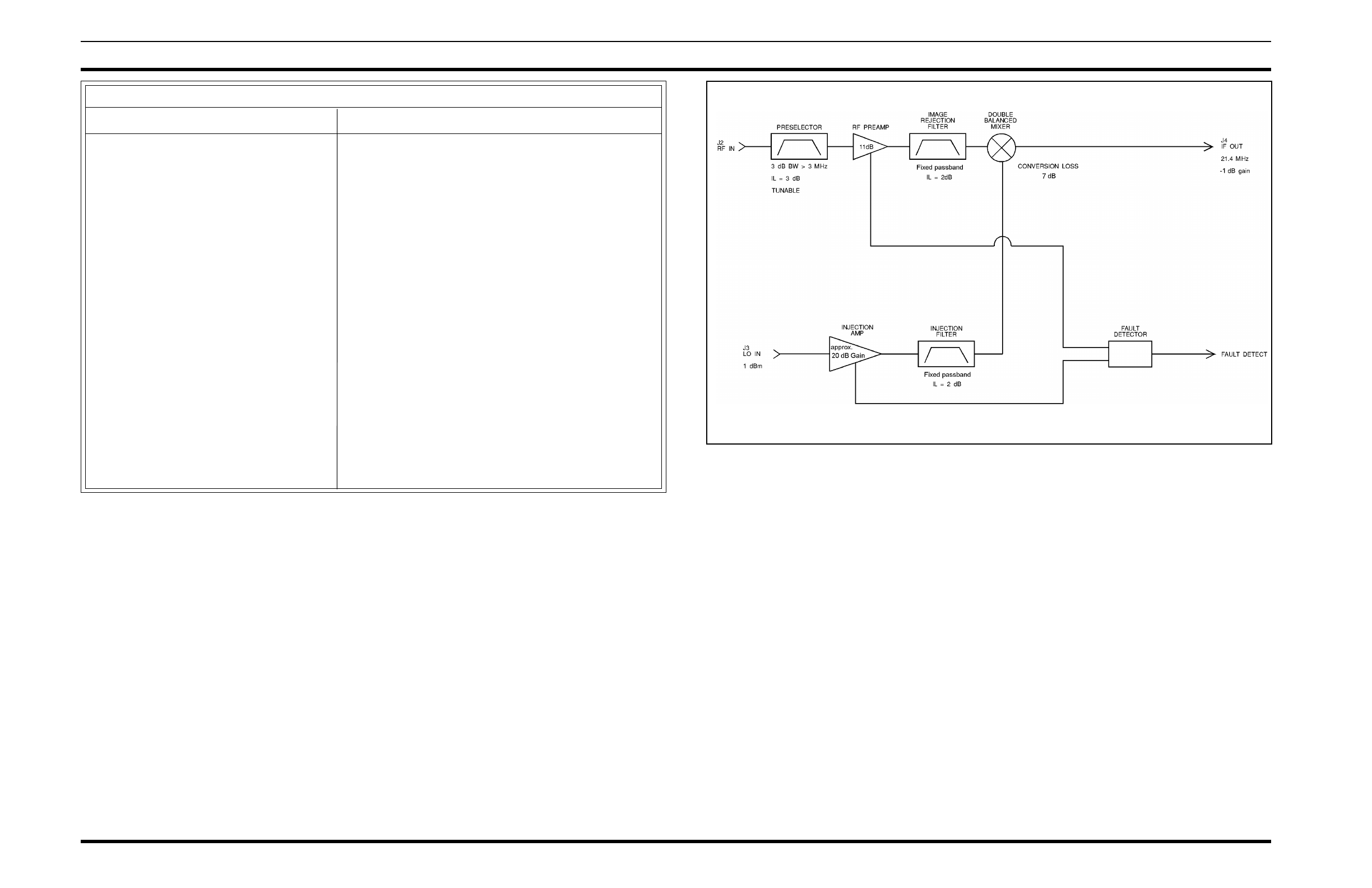
CIRCUIT ANALYSIS
PRESELECTOR FILTER
The received RF signal (J2) is routed through the Prese-
lector Filter (L1 through L5). This filter provides front end
selectivity and attenuates the potential spurious signals of the
first conversion. Typically, the filter has an insertion loss of 3
dB and an operational bandwidth of 2 MHz. The filter is a
tunable, five-pole helical bandpass filter.
PREAMPLIFIER
The output from the Preselector is coupled through an
impedance matching network consisting of C1, C2 and L6 to
the base of Preamplifier Q1. The Preamplifier stage is supplied
by the regulated +12 Vdc line (VCC1) and draws about 80 mA.
It has a low noise figure and high Third Order Intercept point.
Transistor Q2 provides Q1 with a constant current source. The
bias on Q1 is monitored by the Fault Detector circuit via R17.
Capacitors C20 and C21 prevent any RF from entering the fault
circuit. The preamplifier output signal is coupled to the Image
Rejection Filter via an impedance matching network consisting
of C4, C11, L8, L15, R5 and R6.
IMAGE REJECTION FILTER
Following the Preamplifier is the Image Rejection Filter.
The Image Rejection Filter is a fixed tuned helical bandpass
filter. The Filter has an insertion loss of about 2 dB.
INJECTION AMPLIFIER
The local oscillator input (J3) from the Receiver Synthe-
sizer is coupled to monolithic amplifier U2, then to the base of
Q8. The Injection Amplifier, consisting of U2, Q8, and associ-
ated circuitry, is capable of amplifying the injection signal to
approximately 18 to 22 dBm. The amplifier is powered by the
regulated +12 Vdc line (VCC1). Transistor Q7 provides Q8
with a constant current source. The bias on U2 and Q8 is
monitored by the Fault Detector circuit via R21 and R31,
respectively. Capacitors C22, C23 and C26 prevent RF from
entering the fault circuit. The Injection Amplifier output
signal is coupled to the Injection Filter via an impedance
matching network consisting of C8, L13, and resistors R15
and R16.
INJECTION FILTER
Following the Injection Amplifier is the Injection Filter.
The injection filter is a fixed, tuned helical bandpass filter.
It is used to attenuate harmonics of the Injection Amplifier.
The filter has an insertion loss of about 2 dB.
DOUBLE BALANCE MIXER
The Double Balance Mixer (DBM) is a broadband
mixer. It converts an RF signal to the 21.4 MHz first conver-
sion IF frequency. The mixer uses low side (G9, G10) or high
side (G6, G8, G11, G12) injection driven by a local oscillator
signal. The mixer conversion loss is typically about 7 dB.
The IF output signal is then routed through a diplexer circuit
to the output connector (J4).
FAULT DETECTOR
The Fault Detector circuit monitors the operation of the
preamplifier and injection amplifier devices. Operational
amplifiers U1.1 and U1.2 compare the bias on the Preampli-
fier Q1 to preset levels, while U1.3 and U1.4 compare the
bias levels on Injection Amplifiers U2 and Q8.
When the bias for Q1, U2, and Q8 is within the preset
window limits, the output from the comparators is a logic
high level. This high level signal is sent to the Station
Controller on the FLAG 0 line.
If the biasing for the amplifiers is not within the proper
operating range, the fault detector circuit will pull the FLAG
0 line low.
Copyright© November 1994, Ericsson GE Mobile Communications, Inc.
Table 1 - General Specifications
ITEM SPECIFICATION
FREQUENCY RANGE 380 - 400 MHz (G8)
403 - 430 MHz (G11)
470 - 492 MHz (G9)
492 - 512 MHz (G10)
403 - 425 MHz (G6)
370 - 390 MHz (G12)
IF FREQUENCY 21.4 MHz
3 dB BANDWIDTH >3 MHz
IMPEDANCE 50 ohms at RF, LO, and IF Ports
CONVERSION LOSS -1.5 ± 1.5dB
NOISE FIGURE (NF) <7.5 dB
THIRD ORDER INTERCEPT POINT >20 dBm (G9, G10)
>16 dBm (G6, G8, G11, G12)
IMAGE REJECTION >100dB
INJECTION POWER -1.5 ± 1.5dB
TEMPERATURE RANGE -30°C TO +60°C
SUPPLY VOLTAGE 12.0 Vdc
SUPPLY CURRENT 200 mA typical Figure 1 - Block Diagram
LBI-39129B
1
MAINTENANCE
TEST PROCEDURE
Following is a test procedure of the module to verify
proper Conversion Gain :
1. Supply 12 Vdc to pin 15A, B, C. (1C is ground.)
2. Inject the desired RF Frequency into RF IN at a level
of -10 dBm.
3. Inject the desired local oscillator frequency into LO
IN at a level of 0 dBm [LO frequency = RF frequency
- 21.4 MHz (for groups G9, G10), or, LO frequency
= RF frequency + 21.4 MHz (for groups G6, G8,
G11, G12)].
4. Measure the IF OUT power at 21.4 MHz, the ratio of
RF IN to IF OUT should be -1.5 ±1.5 dB.
5. Measure the current drawn by the RXFE module.
Typical current drain is 180 to 230 mA.
ALIGNMENT PROCEDURE
Alignment for the Receiver Front End module consists
of tuning the five-pole Preselector Filter only. The Image
Rejection Filter and LO injection filter are not to be tuned.
Normally, the RXFE should only need the fine-tuning pro-
cedure. For a major receiver frequency change, the RXFE
should be adjusted using the major-retuning procedure.
For Fine-Tuning
1. Supply 12 Vdc to pin 15A, B, C. (1C is ground.)
2. Inject the desired RF Frequency into RF IN (J2) at a
level of -10 dBm.
3. Inject the desired local oscillator frequency into LO
IN (J3) at a level of 0 dBm [LO frequency = RF
frequency - 21.4 MHz (for groups G9, G10), or, LO
frequency = RF frequency + 21.4 MHz (for groups
G6, G8, G11, G12)].
4. Detect IF signal at 21.4 MHz. Slightly adjust L1 to
L5 to get maximum power (don’t adjust more than
1/4 turn). If an RF Voltmeter is used, connect a Low
Pass Filter (LPF)to the IF OUT (J4) to attenuate high
frequency components. The corner of the LPF should
be set for 40 MHz.
5. Repeat Test Procedure steps to verify conversion
gain.
For Major Retuning
The best way to do a major retuning of the RXFE is with
swept frequency tuning. The swept frequency tuning can be
done using a Spectrum Analyzer and Tracking Generator.
With proper Injection level the frequency response of the
Preselector Filter can be seen by viewing the RF to IF port
feedthrough on the spectrum analyzer. This feedthrough is
typically 35 dB down from the input level at the RF port. Use
the following procedure for swept frequency tuning:
1. Supply 12 Vdc to pin 15A, B, C. (1C is ground.)
2. Inject the Tracking generator output at 0 dBm into
the RF IN connector, (J2).
3. Inject local oscillator power at 0 dBm into the LO IN
connector, (J3) [LO frequency = RF frequency - 21.4
MHz (for groups G9, G10), or, LO frequency = RF
frequency + 21.4 MHz (for groups G6, G8, G11,
G12)].
4. Preset the height of slugs with respect to the top of
five-pole cavity as follows (Table 2):
5. Center the spectrum analyzer at the desired frequency
and set the reference at about -30 dBm. Adjust L1 to
L5 for best possible response.
SYMPTOM AREAS TO CHECK READING (TYP.)
LOW CONVERSION GAIN Check Vcc 12 V
Preselector Loss 3 dB
Preamplifier Gain 11 dB
Image Rej. Filter Loss 2 dB
1st Mixer Conversion Loss 7 dB
FAULT INDICATOR LOW Check Vc of Q1 9 TO 10V
Check Vc of U2 5 TO 6 V
Check Vc of Q8 9 TO 10 V
IF FREQUENCY OFF Check L.O. FREQUENCY L.O. frequency=RF frequency - 21.4 MHz (G9,G10)
+ 21.4 MHz (G6, G8, G11, G12)
LOW L.O. POWER* Injection Amplifier Gain approx 20 dB Gain
Injection Filter Loss 2 dB
*NOTE: For troubleshooting the gain or loss, the RXFE needs to be under the normal operating condition:
•12 Vdc supply.
•Inject L.O. power at a level of 0 dBm into LO IN (J3), [LO freq. = RF freq. - 21.4 MHz (G9, G10)
or, LO frequency = RF frequency + 21.4 MHz (G6, G8, G11, G12)].
•Inject the desired RF signal at a level of -10 dBm into RF IN (J2).
•Terminate the IF OUT (J4) with a good 50 ohm impedance.
•Use a Spectrum Analyzer and 50 ohm probe (with good RF grounding) to probe at the input and output of
each stage to check its gain or loss (see schematic diagram).
TROUBLESHOOTING GUIDE
G6 & G11 HEIGHT (in inches)
Frequency
(MHz) L1 L2 L3 L4 L5
403 12/64 10/64 12/64 13/64 12/64
408 13/64 13/64 14/64 14/64 13/64
413 14/64 14/64 14/64 15/64 14/64
418 16/64 16/64 15/64 16/64 15/64
423 17/64 17/64 16/64 18/64 16/64
Table 2
G9 HEIGHT (in inches)
Frequency
(MHz) L1 L2 L3 L4 L5
470 12/64 12/64 12/64 12/64 12/64
474 13/64 13/64 13/64 13/64 13/64
478 14/64 14/64 14/64 14/64 14/64
482 15/64 15/64 15/64 15/64 15/64
486 16/64 16/64 16/64 16/64 16/64
490 17/64 17/64 17/64 17/64 17/64
492 18/64 18/64 18/64 18/64 18/64
G10 HEIGHT (in inches)
Frequency
(MHz) L1 L2 L3 L4 L5
492 12/64 10/64 10/64 10/64 8/64
497 12/64 10/64 12/64 12/64 9/64
502 14/64 12/64 13/64 14/64 10/64
507 15/64 15/64 16/64 16/64 12/64
512 17/64 16/64 17/64 17/64 14/64
G8, G12 HEIGHT (in inches)
Frequency
(MHz) L1 L2 L3 L4 L5
380 16/64 16/64 16/64 16/64 16/64
385 17/64 17/64 17/64 17/64 17/64
390 18/64 18/64 18/64 18/64 18/64
395 19/64 19/64 19/64 19/64 19/64
400 20/64 20/64 20/64 20/64 20/64
370 14/64 14/64 14/64 14/64 14/64
375 15/64 15/64 15/64 15/64 15/64
LBI-39129B
2
RECEIVER FRONT END MODULE
19D902782G6 (403-425 MHz)
19D902782G8 (380-400 MHz)
19D902782G9 (470-494 MHz)
19D902782G10 (492-512 MHz)
19D902782G11 (403-430 MHz)
19D902782G12 (370-390 MHz)
ISSUE 3
PARTS LIST & PRODUCTION CHANGES
SYMBOL PART NO. DESCRIPTION
RECEIVER FRONT END BOARD
19D902782G6, G8-G12
- - - - - - - - - - - DIODES - - - - - - - - - -
CR1 344A3062P1 Diode, Schottky.
- - - - - - - - - MISCELLANEOUS - - - - - - - - -
CR2 19A703595P10 Diode, optoelectric: Red; sim to HP HLMP-1301-010
(Used in G8).
- - - - - - - - - - CAPACITORS - - - - - - - - -
C1 19A702061P37 Ceramic: 33 pF + or -5%, 50 VDCW, temp coef 0 +
or -30 PPM/‘C. (Used in G8, G12).
C1 19A702052P14 Ceramic: 0.01 uF + or - 10%, 50 VDCW. (Used in G6,
G10 and G11).
C1 19A702061P21 Ceramic: 15 pF + or - 5%, 50 VDCW, temp coef 0
+ or - 30 PPM. (Used in G9).
C2 19A702061P17 Ceramic: 12 pF + or - 5%, 50 VDCW, temp coef 0
+ or - 30 PPM. (Used in G6, G8, G11 and G12).
C2 19A702061P21 Ceramic: 15 pF + or - 5%, 50 VDCW, temp coef 0
+ or - 30 PPM. (Used in G9).
C2 19A702061P12 Ceramic: 8.2 pF + or - 0.5 pF, 50 VDCW, temp
or - 60 PPM. (Used in G10).
C3 19A702052P14 Ceramic: 0.01 uF + or - 10%, 50 VDCW.
C7 19A702052P14 Ceramic: 0.01 uF + or - 10%, 50 VDCW. (Used in G8,
G12).
C7 19A702061P33 Ceramic: 27 pF + or - 5%, 50 VDCW, temp coef 0 + or -
30 PPM. (Used in G6 and G11).
C7 19A702236P32 Ceramic: 18 pF + or -5%, 50 VDCW, temp coef 0 + or -30
PPM. (Used in G9).
C7 19A702061P37 Ceramic: 33 pF + or -5%, 50 VDCW, temp coef 0 + or -30
PPM/‘C. (Used in G10).
C8 19A702052P14 Ceramic: 0.01 uF + or - 10%, 50 VDCW. (Used in G6, G8,
G9, G11, and G12).
C8 19A702061P17 Ceramic: 12 pF + or - 5%, 50 VDCW, temp coef 0 + or -
30 PPM. (Used in G10).
C9 19A702061P9 Ceramic: 4.7 pF + or - 0.5 pF, 50 VDCW, temp
or - 60 PPM. (Used in G6, G8, G11 and G12).
C10 19A702061P11 Ceramic: 6.8 pF + or - 0.5 pF, 50 VDCW, temp
or - 60 PPM. (Used in G6, G8, G10, G11 and G12).
C10 19A702236P17 Ceramic: 4.7 pF + or -5%, 50 VDCW, temp coef 0
+ or -30 PPM. (Used in G9).
C11 19A702061P33 Ceramic: 27 pF + or -5%, 50 VDCW, temp coef 0 + or -30
PPM/‘C. (Used in G10).
C12 19A702052P14 Ceramic: 0.01 uF + or - 10%, 50 VDCW. (Used in G6, G8,
G11 and G12).
C12 19A702061P8 Ceramic: 3.9 pF + or - 0.5 pF, 50 VDCW, temp
or - 120 PPM. (Used in G9 and G10).
C20
thru
C26
19A702052P14 Ceramic: 0.01 uF + or - 10%, 50 VDCW.
C28 19A702052P14 Ceramic: 0.01 uF + or - 10%, 50 VDCW.
C29
and 19A702061P89 Ceramic: 1500 pF + or - 5%, 50 VDCW, temp coef - 30
PPM.
C30
C31
thru
C33
19A702236P40 Ceramic: 39 pF + or -5%, 50 VDCW, temp coef 0 + or -30
PPM.
C34
thru
C36
19A702061P37 Ceramic: 33 pF + or -5%, 50 VDCW, temp coef 0 + or -30
PPM/‘C.
C37
and
C38
19A705205P26 Tantalum: 3.3 uf + or - 20%, 16 VDCW. (Used in G8, G10
and G11).
SYMBOL PART NO. DESCRIPTION
C39
and
C40
19A705205P15 Tantalum: 33 uf + or - 20%, 16 VDCW. (Used in G8, G10
and G11).
- - - - - - - - - - - FILTERS - - - - - - - - - -
FL1 19A705458P8 Helical, 378-402 MHz. (Used in G8).
FL1 19A705458P4 Helical, UHF: 403-425 MHz. (Used in G6).
FL1 19A705458P9 Helical, 403-430 MHz. (Used in G11).
FL1 19A705458P2 Helical, UHF: 470-492 MHz. (Used in G9).
FL1 19A705458P6 Helical, UHF: 492-515 MHz. (Used in G10).
FL1 19A705458P13 Helical, UHF: 391-415 MHz. (Used in G12).
FL2 19A705458P4 Helical, UHF: 403-425 MHz. (Used in G8).
FL2 19A705458P5 Helical, UHF: 424-450 MHz. (Used in G6 and G11).
FL2 19A705458P1 Helical, UHF: 450-470 MHz. (Used in G9).
FL2 19A705458P2 Helical, UHF: 470-492 MHz. (Used in G10).
FL2 19A705458P12 Helical, UHF: 370-390 MHz. (Used in G12).
- - - - - - - - - MISCELLANEOUS - - - - - - - - -
J1 19B801587P7 Connector, Din: 96 male contacts, right angle mounting;
sim to AMP 650889-1.
J2
thru
J4
19A115938P24 Connector, receptacle.
- - - - - - - - - - INDUCTORS - - - - - - - - - -
L1 19C850817P30 Coil, RF. (Used in G8).
L1 19C850817P29 Coil, RF. (Used in G6 and G11).
L1 19C850817P3 RF Coil: sim to Paul Smith SK853-1. (Used in G9).
L1 19C850817P18 RF Coil: sim to Paul Smith SK853-1. (Used in G10).
L2 19C850817P31 Coil. RF. (Used in G8).
L2 19C850817P5 RF Coil: sim to Paul Smith SK853-1. (Used in G6 and
G11).
L2 19C850817P4 RF Coil: sim to Paul Smith SK853-1. (Used in G9).
L2 19C850817P17 RF Coil: sim to Paul Smith SK853-1. (Used in G10).
L3 19C850817P31 RF Coil: (Used in G8).
L3 19C850817P5 RF Coil: sim to Paul Smith SK853-1. (Used in G6
andG11).
L3 19C850817P4 RF Coil: sim to Paul Smith SK853-1. (Used in
G9).
L3 19C850817P17 RF Coil: sim to Paul Smith SK853-1. (Used in
G10).
L4 19C850817P31 Coil, RF. (Used in G8).
L4 19C850817P5 RF Coil: sim to Paul Smith SK853-1. (Used in G6 and
G11).
L4 19C850817P4 RF Coil: sim to Paul Smith SK853-1. (Used in G9).
L4 19C850817P17 RF Coil: sim to Paul Smith SK853-1. (Used in G10).
L5 19C850817P30 Coil, RF. (Used in G8).
L5 19C850817P29 Coil, RF. (Used in G6and G11).
L5 19C850817P3 RF Coil: sim to Paul Smith SK853-1. (Used in G9).
L5 19C850817P18 RF Coil: sim to Paul Smith SK853-1. (Used in G10).
L6 19A705470P4 Coil, Fixed: 18 nH; sim to Toko 380NB-18nM.
(Used in G8, G12).
L6 19A705470P1 Coil, Fixed: 10 nH; sim to Toko 380NB-10nM.
(Used in G6, G9 and G11).
L6 19A705470P5 Coil, Fixed: 22 nH; sim to Toko 380NB-22nM.
(Used in G10).
L7 19A705470P16 Coil, Fixed: 0.18 uH; sim to Toko 380NB-R18M.
L8 19A705470P12 Coil, fixed: 82nH; sim to Toko 380NB-82nM. (Used in G8,
G12).
L8 19A705470P11 Coil, fixed: 68 nH; sim to Toko 380NB-68nM. (Used in G6
and G11).
L8 19A705470P6 Coil: 27 nH; sim to Toko 380NB-27nM. (Used in G9 and
G10).
L9 19A705470P6 Coil: 27 nH; sim to Toko 380NB-27nM. (Used in G8 and
G9, G12).
SYMBOL PART NO. DESCRIPTION
L9 19A705470P14 Coil, fixed: 0.12 uH; sim to Toko 380NB-R12M. (Used
in G6 and G11).
L9 19A705470P1 Coil, fixed: 10 nH; sim to Toko 380NB-10nM. (Used in
G10).
L10 19A705470P16 Coil, fixed: 0.18 nH; sim to Toko 380NB-R18M.
L11 19A705470P16 Coil, fixed: 0.18 nH; sim to Toko 380NB-R18M. (Used
in G8 and G12).
L11 19A705470P1 Coil, fixed: 10 nH; sim to Toko 3 80NB-10nM.(Used in
G6 and G11).
L11 19A705470P48 Coil, fixed: 82 uH; sim to TOKO 380KB-820K. (Used in
G9).
L11 19A705470P7 Coil, fixed: 33 nH + or -20%; sim to Toko
380NB-33nM. (Used in G10).
L12 19A705470P16 Coil, fixed: 0.18 uH; sim to Toko 380NB-R18M.
L13 19A705470P10 Coil, fixed: 56 nH; sim to Toko 380NB-56nM.
(Used in G6 and G11).
L14 19A705470P4 Coil, fixed: 18 nH; sim to Toko 380NB-18nM.
(Used in G6, G8, G11 and G12).
L14
and
L15
19A705470P6 Coil: 27 nH; sim to Toko 380NB-27nM. (Used in G10).
L21 19A705470P16 Coil, fixed: 0.18 uH; sim to Toko 380NB-R18M.
L22 19A700021P105 Coil, RF: fixed. (Used in G6, G8, G10, and G11).
L22 19A700021P106 Coil, RF. (Used in G9).
L23 19A700021P13 Coil, RF: fixed, 470 nH.
L24 19A700000P122 Coil, fixed: 8.2 uF + or -10%; sim to Jeffers 22-8.2-10
(Used in G8, G10 and G11).
- - - - - - - - - - TRANSISTORS - - - - - - - - -
Q7 19A700059P2 Silicon, PNP: sim to MMBT3906, low profile.
Q8 344A3058P1 Silicon, NPN.
- - - - - - - - - - RESISTORS - - - - - - - - - -
R1 19B800607P332 Metal film: 3.3K ohms + or -5%, 1/8 w. (Used in G8).
R1 19B800607P183 Metal film: 18K ohms + or -5%, 1/8 w. (Used in G6,
G9, G10, and G11).
R2 19B800607P102 Metal film: 1K ohms + or -5%, 1/8 w.
R3 19B800607P331 Metal film: 330 ohms + or -5%, 1/8 w.
R4 19B800607P560 Metal film: 56 ohms + or -5%, 1/8 w.
R5 19B800607P1 Metal film: Jumper. (Used in G8 , G9 and G12).
R5 19B800607P100 Metal film: 10 ohms + or -5%, 1/8 w. (Used in G6 and
G11).
R6 19B800607P101 Metal film: 100 ohms + or -5%, 1/8 w. (Used in G8,
G12).
R6 19B800607P391 Metal film: 390 ohms + or -5%, 1/8 w. (Used in G6 and
G11).
R7 19B800607P201 Metal film: 200 ohms + or -5%, 1/8 w.
R8 19B800607P121 Metal film: 120 ohms + or -5%, 1/8 w.
R9 19B800607P100 Metal film: 10 ohms + or -5%, 1/8 w. (Used in G6, G8
G11 and G12).
R9 19B800607P1 Metal film: Jumper. (Used in G9 and G10).
R10 19B800607P101 Metal film: 100 ohms + or -5%, 1/8 w. (Used in G8,
G12).
R10 19B800607P391 Metal film: 390 ohms + or -5%, 1/8 w. (Used in G6 and
G11).
R11 19B800607P332 Metal film: 3.3K ohms + or -5%, 1/8 w.
R12 19B800607P562 Metal film: 5.6K ohms + or -5%, 1/8 w.
R13 19B800607P122 Metal film: 1.2K ohms + or -5%, 1/8 w.
R14 19B800607P390 Metal film: 39 ohms + or -5%, 1/8 w. (Used in G8 ,
G10, and G12).
R14 19B800607P560 Metal film: 56 ohms + or -5%, 1/8 w. (Used in G6 and
G11).
R14 19B800607P330 Metal film: 33 ohms + or -5%, 1/8 w. (Used in G9).
R15 19B800607P1 Metal film: Jumper. (Used in G8, G9, G10, and G12).
SYMBOL PART NO. DESCRIPTION
R15 19B800607P100 Metal film: 10 ohms + or -5%, 1/8 w. (Used in G6 and
G11).
R16 19B800607P101 Metal film: 100 ohms + or -5%, 1/8 w. (Used in G8,
G12).
R16 19B800607P391 Metal film: 390 ohms + or -5%, 1/8 w. (Used in G6 and
G11).
R17 19B800607P103 Metal film: 10K ohms + or -5%, 1/8 w.
R18 19B800607P562 Metal film: 5.6K ohms + or -5%, 1/8 w.
R19 19B800607P183 Metal film: 18K ohms + or -5%, 1/8 w.
R20 19B800607P333 Metal film: 33K ohms + or -5%, 1/8 w.
R21 19B800607P103 Metal film: 10K ohms + or -5%, 1/8 w.
R22 19B800607P272 Metal film: 2.7K ohms + or -5%, 1/8 w.
R23 19B800607P152 Metal film: 1.5K ohms + or -5%, 1/8 w.
R24 19B800607P153 Metal film: 15K ohms + or -5%, 1/8 w.
R25 19B800607P390 Metal film: 39 ohms + or -5%, 1/8 w. (Used in G8,
G10, and G12).
R25 19B800607P560 Metal film: 56 ohms + or -5%, 1/8 w. (Used in G6 and
G11).
R25 19B800607P330 Metal film: 33 ohms + or -5%, 1/8 w. (Used in G9).
R26 19B800607P560 Metal film: 56 ohms + or -5%, 1/8 w.
R27 19B800607P121 Metal film: 120 ohms + or -5%, 1/8 w.
R28 19B800607P103 Metal film: 10K ohms + or -5%, 1/8 w.
R29 19B800607P682 Metal film: 6.8K ohms + or -5%, 1/8 w.
R30 19B800607P201 Metal film: 200 ohms + or -5%, 1/8 w.
R31 19B800607P103 Metal film: 10K ohms + or -5%, 1/8 w.
R32 19B800607P101 Metal film: 100 ohms + or -5%, 1/8 w. (Used in G8).
R32 19B800607P331 Metal film: 330 ohms + or -5%, 1/8 w. (Used in G10).
R32 19B800607P201 Metal film: 200 ohms + or -5%, 1/8 w. (Used in G12).
R33 19B800607P510 Metal film: 51 ohms + or -5%, 1/8 w.
- - - - - - - - - - TRANSFORMERS - - - - - - - -
T1 344A3063P1 Transformer.
and
T2 - - - - - - - INTEGRATED CIRCUITS - - - - - - -
U2 344A3907P1 Integrated circuit, MMIC: sim to Avantek
MSA-1105.
- - - - - - - - - MISCELLANEOUS - - - - - - - - -
4 19D902555P1 Handle.
6 19A702381P1506 Screw, thread forming: Torx, No. M3.5-.6 x 6.
7 19A702381P1513 Screw, thread forming: Panhead..
11 19A702381P1508 Screw, thread forming: No. 3.5-0.6 x 8.
20 19B800701P2 Tuning screw.
21 19A701800P1 Stop nut.
22 19D902467P2 Casting.
27 19D902508P5 Chassis..
28 19D902534P2 Cover, RF.
29 19D904572P1 Gasket.
30 19B802690P1 Grommet.
* COMPONENTS, ADDED, DELETED OR CHANGED BY PRODUCTION CHANGES
PRODUCTION CHANGES
Changes in the equipment to improve performance or to simplify circuits are identified by
a "Revision Letter", which is stamped after the model number on the unit. The revision
stamped on the unit includes all previous revisions. Refer to the Parts List for the descrip-
tion of parts affected by these revisions.
REV. A - RECEIVER FRONT END BOARD 19D902490G6
RECEIVER FRONT END BOARD 19D902490G11
Add new splits. PWB changed.
REV. A - RECEIVER FRONT END BOARD 19D902490G8
REV. B - RECEIVER FRONT END BOARD 19D902490G11 & G10
To eliminate receiver spurious response at 100 kHz switching power
supply frequency. Added C37 thru C40 and L24.
LBI-39129B
3
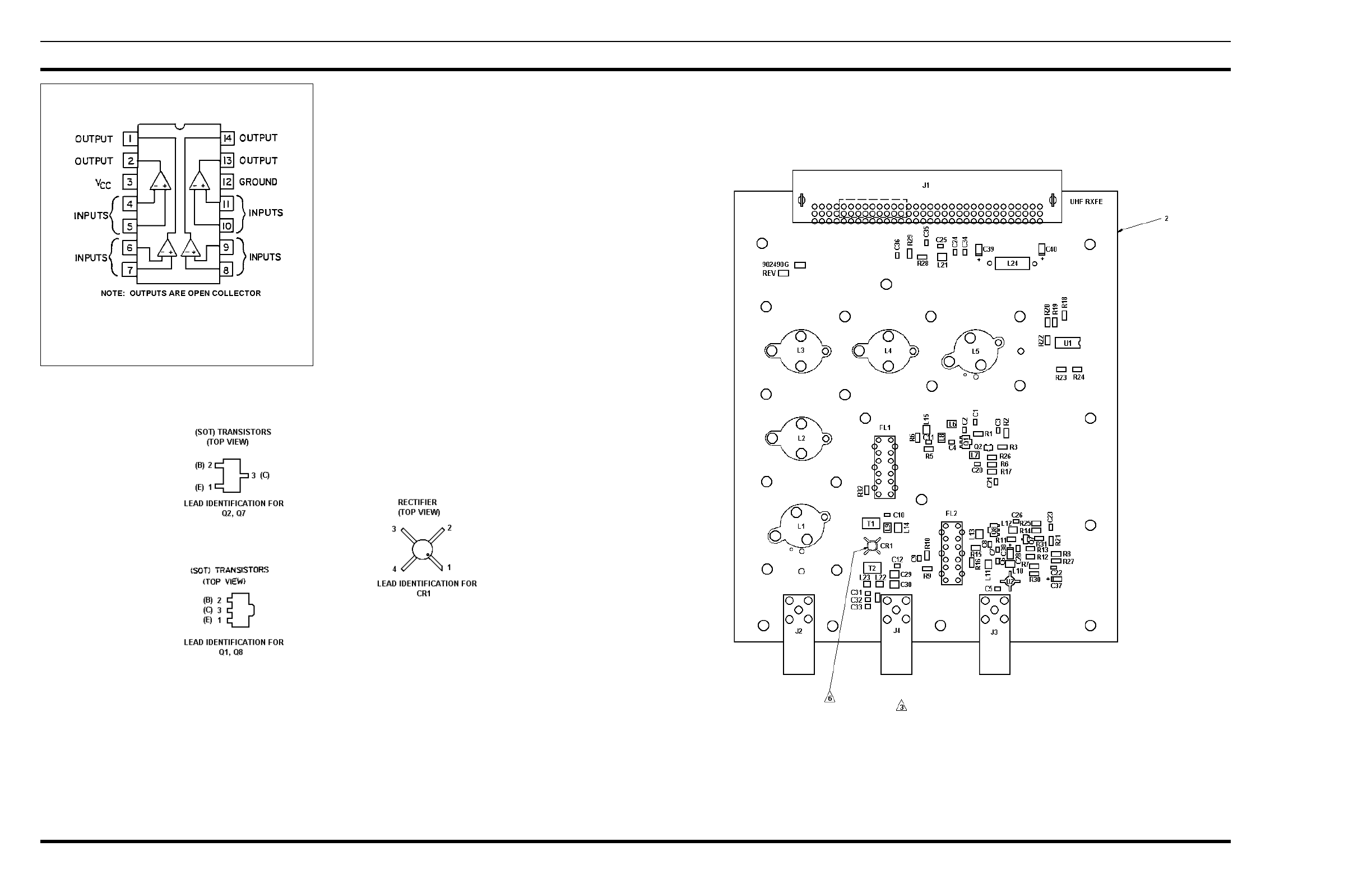
OUTLINE DIAGRAM
U1
19A704125P1
Quad Operational Amplifier
(19D902490, Sh. 7, Rev. 5)
RECEIVER FRONT END BOARD
19D902490G6, G8 - G12
LBI-39129B
4
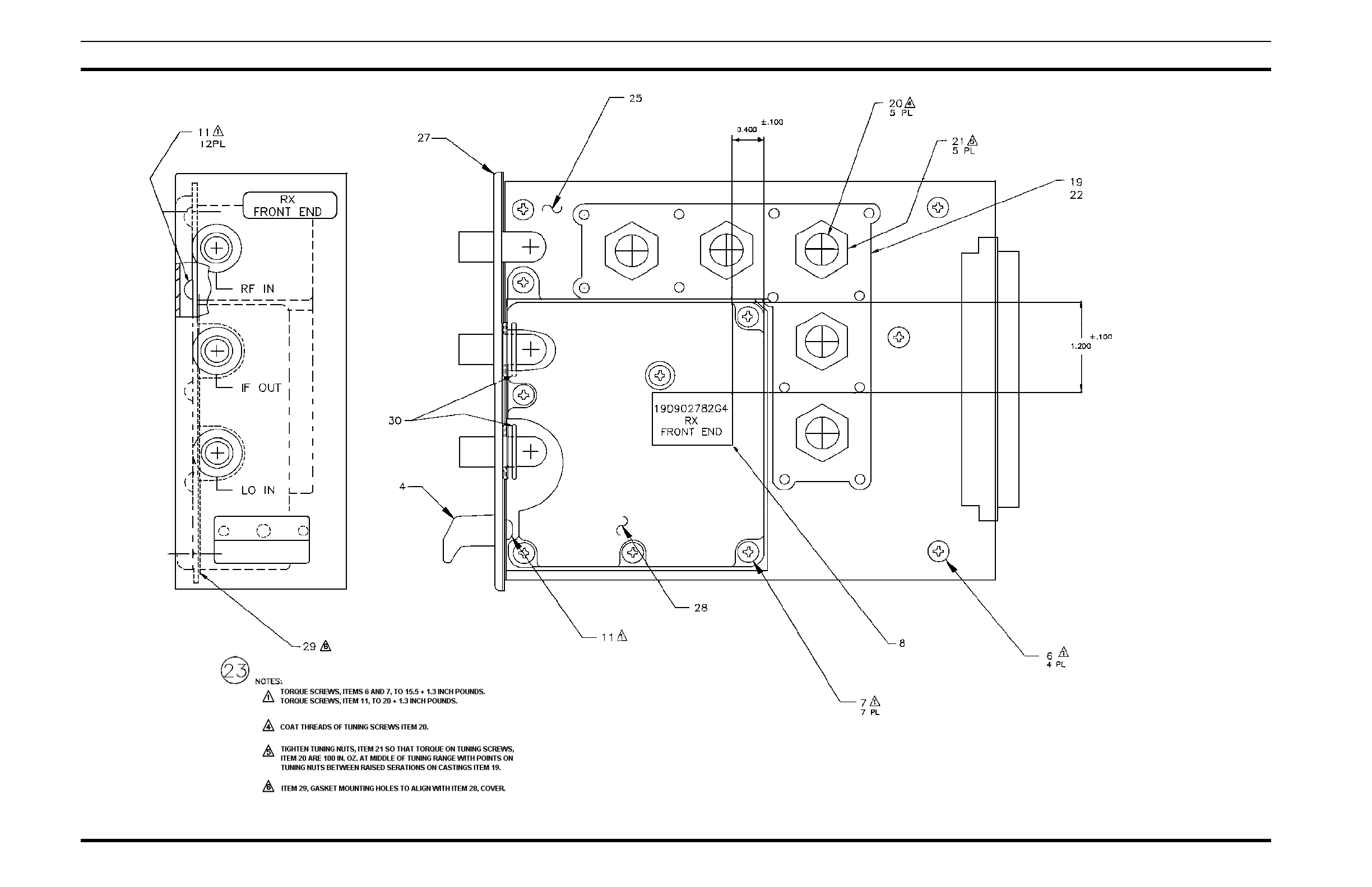
ASSEMBLY DIAGRAM
RECEIVER FRONT END MODULE
19D902782G6, G8 - G12
(19D902782 Sh.2 Rev.3)
LBI-39129B
5
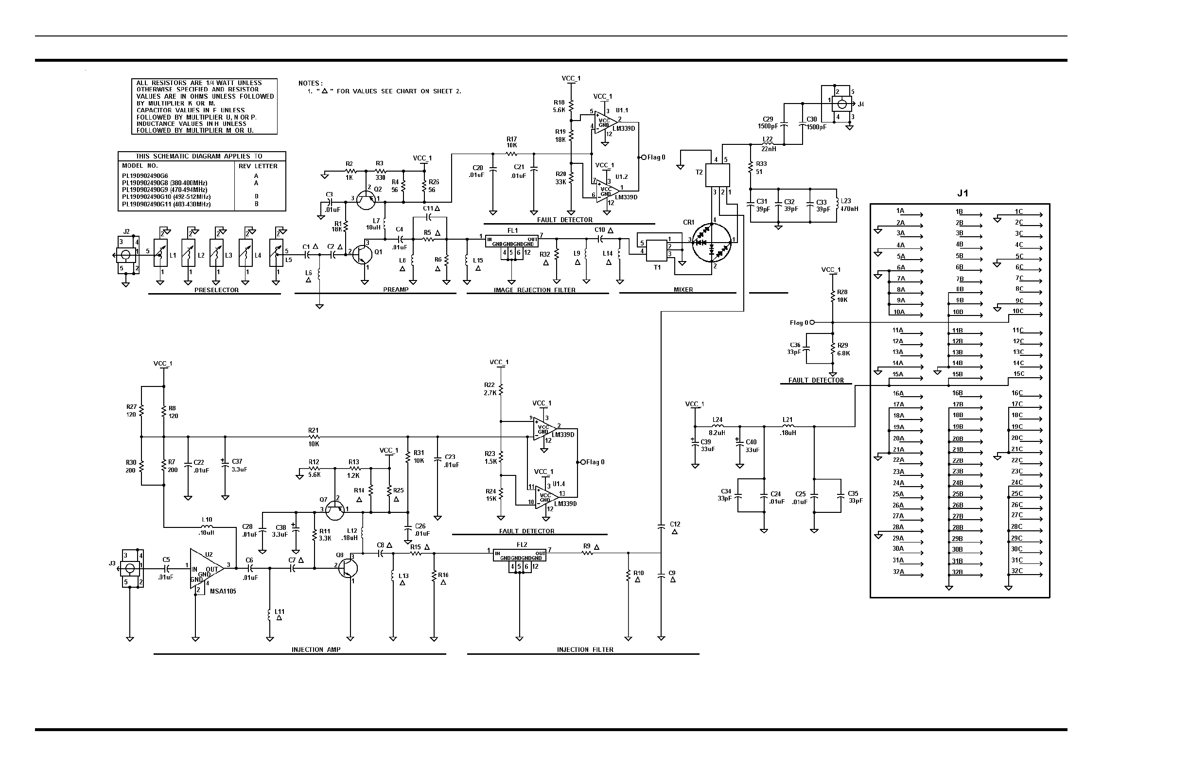
SCHEMATIC DIAGRAM
RECEIVER FRONT END MODULE
19D902782G6, G8-G12
(188D5789 Sh.1, Rev. 6A)
LBI-39129B
6
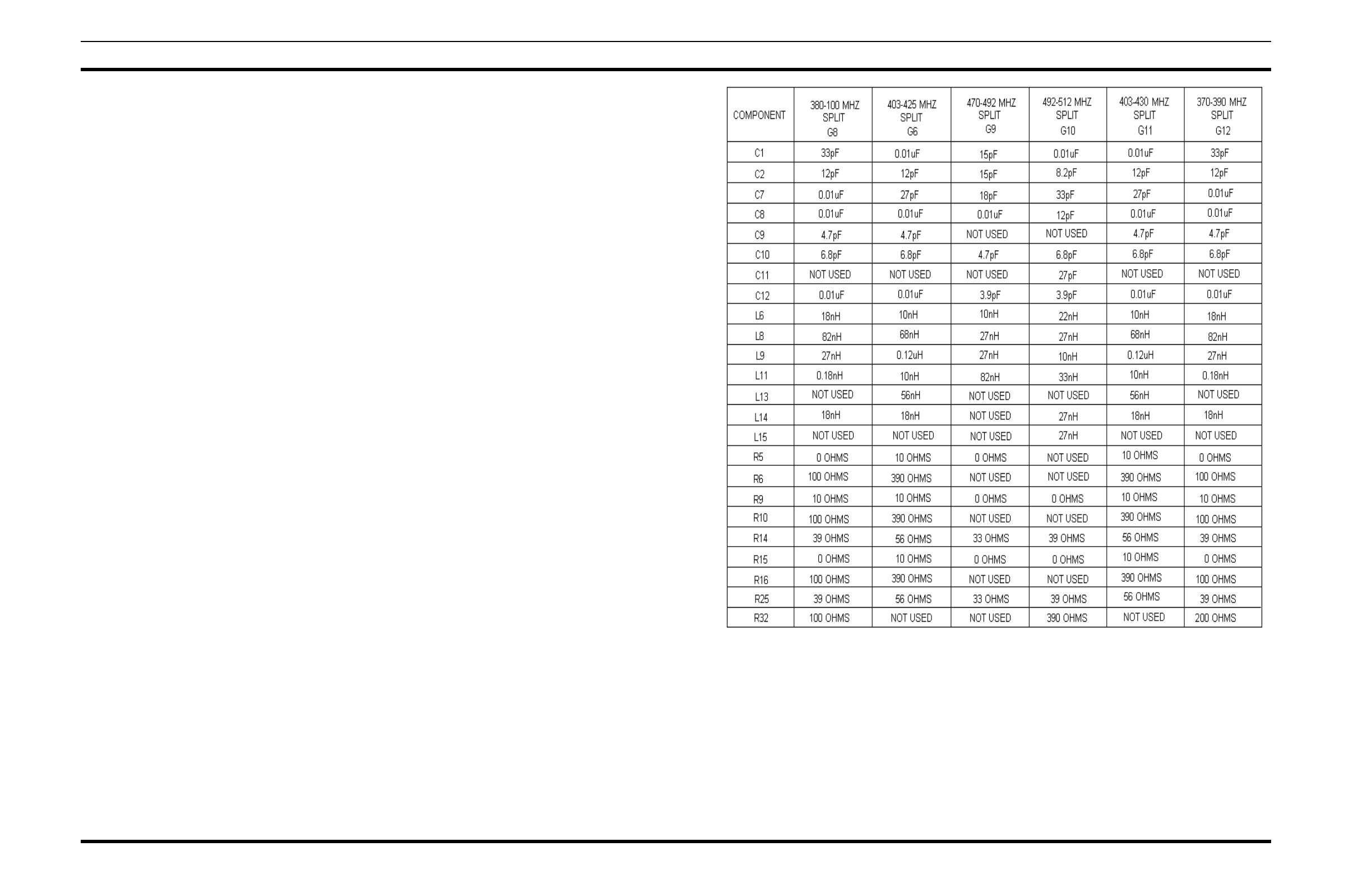
SCHEMATIC DIAGRAM
RECEIVER FRONT END MODULE
19D902782G6, G8 - G12
(188D5789 Sh.2, Rev. 6A)
LBI-39129B
7